JP2007201540A - Optical signal transmitter - Google Patents
Optical signal transmitter Download PDFInfo
- Publication number
- JP2007201540A JP2007201540A JP2006014041A JP2006014041A JP2007201540A JP 2007201540 A JP2007201540 A JP 2007201540A JP 2006014041 A JP2006014041 A JP 2006014041A JP 2006014041 A JP2006014041 A JP 2006014041A JP 2007201540 A JP2007201540 A JP 2007201540A
- Authority
- JP
- Japan
- Prior art keywords
- signal
- optical
- light source
- output
- optical signal
- Prior art date
- Legal status (The legal status is an assumption and is not a legal conclusion. Google has not performed a legal analysis and makes no representation as to the accuracy of the status listed.)
- Pending
Links
Images

Landscapes
- Optical Communication System (AREA)
Abstract
Description
本発明は、間欠的に生じる光信号を生成するための光信号送信装置に関し、特にバースト通信用の光信号送信装置に関する。 The present invention relates to an optical signal transmitter for generating an optical signal generated intermittently, and more particularly to an optical signal transmitter for burst communication.
複数の光信号を異なる波長の光に乗せ、1本の光ファイバで伝送する波長分割多重(WDM:Wavelength Division Multiplexing)伝送システムは、伝送路の容量を大幅に増大させることが可能であり、既に基幹系システムを中心に導入が進んでいる。さらに近年、光信号の波長を、伝送路容量の増大に適用するだけでなく、ネットワークの経路設定にも用いる波長ルーティングの開発や導入検討も進んでいる。 A wavelength division multiplexing (WDM) transmission system in which a plurality of optical signals are placed on light of different wavelengths and transmitted through a single optical fiber can greatly increase the capacity of the transmission path, Introduction is progressing mainly in mission-critical systems. Furthermore, in recent years, not only is the wavelength of an optical signal applied to an increase in transmission path capacity, but also development and introduction of wavelength routing that is used for setting a network path has been advanced.
このような、波長情報を活用したフォトニックネットワークシステムにおいて、ネットワーク資源を無駄なく効率的に利用するためには、バースト通信と呼ばれる手法の適用が効果的である。 In such a photonic network system utilizing wavelength information, in order to efficiently use network resources without waste, application of a technique called burst communication is effective.
バースト通信では、送信するデータを宛先毎にまとめ、一連のデータの塊として送受信を行う。このバースト通信を、波長情報を活用したフォトニックネットワークに適用する場合、波長可変光源を内蔵する送信器を使用し、宛先毎にまとめられたデータを、適切な波長の信号として送出することになる。このようなバースト通信に対応せず、波長可変光源を使用しない旧来のフォトニックネットワークシステムでは、トラフィックが少ない経路に対しても全て固有の光源を割当てる必要があり、ネットワーク資源の利用効率が低くなってしまっていた。一方、バースト通信を適用すれば、トラフィックが比較的少ない経路で使用していた複数の送信器の代わりに、波長可変光源を内蔵する送信器を使用することができ、ネットワーク資源の利用効率を向上させられることとなる(非特許文献1)。 In burst communication, data to be transmitted is collected for each destination, and transmitted and received as a series of data chunks. When this burst communication is applied to a photonic network that utilizes wavelength information, a transmitter that incorporates a wavelength tunable light source is used, and data collected for each destination is transmitted as a signal of an appropriate wavelength. . In a conventional photonic network system that does not support such burst communication and does not use a wavelength tunable light source, it is necessary to assign a unique light source even to a route with low traffic, and the use efficiency of network resources is reduced. It was. On the other hand, if burst communication is applied, it is possible to use a transmitter with a built-in wavelength tunable light source instead of multiple transmitters that were used on a route with relatively little traffic, improving network resource utilization efficiency. (Non-Patent Document 1).
しかしながら、バースト通信に用いる信号の生成は容易ではない。図4に従来の典型的な高ビットレートな光信号送信装置の構成を示す。図4において、401は光源、402は外部変調器、403は電気のデータ信号を入力するデータ信号入力ポート、404はバイアス電源、405は外部変調器用ドライバ回路、および406は光信号出力ポートである。データ信号入力ポート403から入力された電気信号であるデータ信号は、外部変調器用ドライバ回路405に入力されて適切な所望の振幅に増幅され、この増幅されたデータ信号は、さらにバイアス電源404から外部変調器用ドライバ回路405に供給される直流電圧に応じて、適切な平均電圧の信号として外部変調器用ドライバ回路405から出力される。外部変調器用ドライバ回路405から出力された電気信号は外部変調器402に入力される。外部変調器402は、その入力された電気信号に応じて、光源401から入力された光信号を透過・遮断させ、光信号出力ポート406から出力させる。以上のようにして、一般的な高ビットレートな光信号が生成される。
However, it is not easy to generate a signal used for burst communication. FIG. 4 shows a configuration of a conventional typical high bit rate optical signal transmission apparatus. In FIG. 4, 401 is a light source, 402 is an external modulator, 403 is a data signal input port for inputting an electrical data signal, 404 is a bias power supply, 405 is a driver circuit for an external modulator, and 406 is an optical signal output port. . A data signal, which is an electrical signal input from the data
だが、図4で説明したこの従来装置をバースト通信に用いる信号の生成に用いる場合、一連のデータの塊と、次の一連のデータの塊と塊の間に存在する無信号状態を生成することが困難である。その理由は、一般的な外部変調器用ドライバ回路405においては、故障を避けるために、電気のデータ信号源(データ信号入力ポート)403から入力されるデータ信号の低周波成分を遮断して増幅するためである。無信号状態を含むバースト通信に用いる信号は多くの低周波成分を含むため、バースト通信に用いる信号を電気のデータ信号入力ポート403から外部変調器用ドライバ回路405に入力しても、外部変調器402から出力される光信号は、波形が歪んでしまう。
However, when the conventional apparatus described in FIG. 4 is used to generate a signal used for burst communication, a series of data chunks and a no-signal state existing between the next series of data chunks are created. Is difficult. The reason is that in a general external
以上のような理由で、従来技術による光信号送信装置を使用する場合に、バースト通信に用いる信号の生成は困難であるという解決すべき課題があった。 For the reasons described above, there has been a problem to be solved that it is difficult to generate a signal used for burst communication when an optical signal transmission apparatus according to the prior art is used.
本発明は、上述の課題を解決するためになされたものであり、その目的は、バースト通信をフォトニックネットワークシステムへ適用するのに適した、無信号状態を含む光信号を波形の歪みなく生成することのできる、光信号送信装置を提供することにある。 The present invention has been made to solve the above-described problems, and an object of the present invention is to generate an optical signal including no signal state suitable for applying burst communication to a photonic network system without waveform distortion. It is an object of the present invention to provide an optical signal transmission device capable of performing the above.
上記の目的を達成するために本発明の信号送信装置は、第1の電気信号を外部から入力する第1の入力ポートと、前記第1の電気信号とタイミングが取れている第2の電気信号を外部から入力する第2の入力ポートであって、該第2の電気信号は意味あるデータの塊と塊の間に、データ信号速度と同程度の速度の信号を挿入して低周波の信号成分を削除した信号である、第2の入力ポートと、光信号を発生する光源であって、前記第1の電気信号によって該光信号の透過/遮断を切り換える光ゲートを内部に有する光源と、前記光源からの入力光信号の透過/遮断を前記第2の電気信号による入力電圧に応じて切り換える外部変調器と、前記外部変調器から出力される光信号を装置からの出力信号として外部に出力する出力ポートと、を具備することを特徴とする。 In order to achieve the above object, a signal transmission device of the present invention includes a first input port for inputting a first electric signal from the outside, and a second electric signal timed with the first electric signal. Is input from the outside, and the second electric signal is a low-frequency signal by inserting a signal having a speed similar to the data signal speed between meaningful data blocks. A second input port that is a signal from which a component has been deleted; a light source that generates an optical signal, and a light source that internally includes an optical gate that switches between transmission and blocking of the optical signal by the first electrical signal; An external modulator that switches transmission / cutoff of an input optical signal from the light source according to an input voltage by the second electric signal, and an optical signal output from the external modulator is output to the outside as an output signal from the device An output port And wherein the Rukoto.
前記第1の電気信号は光信号送信装置から送信するデータの包絡線に相当する信号であるとすることができる。 The first electric signal may be a signal corresponding to an envelope of data transmitted from the optical signal transmission device.
また、前記光信号送信装置において、前記光源は、外部から入力される第3の電気信号によって、出力光の波長が制御される波長可変光源であってもよく、また、前記光ゲートは出力信号のレベルを調節する機能を併せ持っていてもよい。 In the optical signal transmission device, the light source may be a wavelength tunable light source in which the wavelength of output light is controlled by a third electric signal input from the outside, and the optical gate may be an output signal. You may also have a function to adjust the level.
さらに、前記光信号送受信装置において、前記光ゲートを含む前記光源は一体に集積されていても、前記光ゲートを含む前記光源と前記外部変調器とが一体に集積されていてもよい。 Furthermore, in the optical signal transmitting / receiving apparatus, the light source including the optical gate may be integrated, or the light source including the optical gate and the external modulator may be integrated.
上記構成により、本発明によれば、特殊な装置を使用することなく、バースト通信をフォトニックネットワークシステムへ適用するのに適した、無信号状態を含む光信号を波形の歪みなく生成することのできる、光信号送信装置を実現できる。 With the above configuration, according to the present invention, an optical signal including a no-signal state suitable for applying burst communication to a photonic network system can be generated without distortion of a waveform without using a special device. An optical signal transmission device that can be realized.
以下、図面を参照して、本発明の実施の形態を詳細に説明する。
[第1の実施形態]
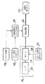
図1を参照して、本発明に係る光信号送信装置の第1の実施の形態を説明する。図1に示す光信号送信装置は、光信号を生成する光源101と、外部変調器102と、電気のデータ信号を入力するデータ信号入力ポート103と、バイアス電源104と、外部変調器用ドライバ回路105と、光信号を外部に出力する光信号出力ポート106と、光ゲート制御信号を入力する光ゲート制御信号入力ポート109とを含む。
Hereinafter, embodiments of the present invention will be described in detail with reference to the drawings.
[First Embodiment]
A first embodiment of an optical signal transmission apparatus according to the present invention will be described with reference to FIG. 1 includes a
光源101は、光信号を生成するレーザ107と、光ゲート制御信号によってレーザ107の出力光の透過/遮断を切り換える光ゲート108とを内部に有する。光ゲート108からの出力光は光源101の出力光として、外部変調器102に入力される。
The
データ信号入力ポート103から入力する電気のデータ信号は、以下で更に詳述するように、光ゲート制御信号とタイミングがとれている信号で有り、かつ意味あるデータの塊と塊の間に、データ信号速度と同程度の速度の信号を挿入して低周波の信号成分を削除した信号である。
The electrical data signal input from the data
データ信号入力ポート103から入力された電気信号であるデータ信号は、外部変調器用ドライバ回路105に入力されて適切な所望の振幅に増幅され、この増幅されたデータ信号は、さらにバイアス電源104から外部変調器用ドライバ回路105に供給される直流電圧に応じて、適切な平均電圧の電気信号として外部変調器用ドライバ回路105から出力される。外部変調器用ドライバ回路105から出力された適切な平均電圧の電気信号は外部変調器102に入力される。外部変調器102は、その入力電圧に応じて、光源101から入力された光信号を透過・遮断させ、光信号出力ポート106から出力させる。このように、外部変調器102は光源101からの入力光信号の透過/遮断を電気のデータ信号による入力電圧に応じて切り換える。
A data signal, which is an electrical signal input from the data
以上の構成において、光源101内部のレーザ107として、例えば半導体の分布帰還型(DFB)レーザを使用することができる。光ゲート108として、例えば半導体光増幅器(SOA)を使用することができる。外部変調器102としては、例えばニオブ酸リチウム(LiNO3)結晶を用いた変調器や、半導体を用いた電界吸収型の変調器等を使用することができる。外部変調器用ドライバ回路105としては、例えば低周波成分の除去された信号を増幅する増幅部と、出力信号の平均電圧を調整するバイアス回路を組み合わせた回路を使用できる。ただし、これらは本実施形態の機能を実現するために使用可能な装置の一例に過ぎず、同様の機能を実現する他の装置を使用する場合も、本発明に含まれる。また、光源101の内部のレーザ107と、光ゲート108と、外部変調器102の一部または全ては、一体に集積されたデバイスであってもよい。
In the above configuration, for example, a semiconductor distributed feedback (DFB) laser can be used as the
本実施形態において、電気のデータ信号入力ポート103から入力される信号は、送信するデータを含み、かつ低周波の信号成分が多くない信号とする。本来バースト通信に用いる信号のみでは、送信するデータである一連のデータの塊と塊の間に信号の無い状態が続くため、低周波の信号成分を多く含む。これに対し、本発明に係るデータ信号入力ポート103から入力される信号は、意味のあるデータである一連のデータの塊と塊の間に、データ信号速度と同程度の速度の、例えば1/0交番信号や、ランダム信号などを挿入することにより、低周波の信号成分を削減した信号である。
In the present embodiment, the signal input from the electrical data
以上のようにして、低周波の信号成分の削除された電気信号は、外部変調器用ドライバ回路105において歪まずに増幅される。増幅され、適当な平均電圧に調整された外部変調路用ドライバ回路105からの出力信号は、外部変調器102に入力され、同時に外部変調器102に入力された光信号の透過・遮断を制御する。
As described above, the electric signal from which the low-frequency signal component has been deleted is amplified without distortion in the external
一方、光ゲート制御信号入力ポート108から入力される光ゲート制御信号は、本光信号送信装置から送信するデータの包絡線に相当する信号とする。この光ゲート制御信号を、光源101の内部にある光ゲート108に入力することで、レーザ107から出力される光信号の透過・遮断を制御する。光ゲート108から出力された光信号は、外部変調器102に入力される。
On the other hand, the optical gate control signal input from the optical gate control
電気のデータ信号入力ポート103から入力される信号と、光ゲート制御信号入力ポート108から入力される信号のタイミングを合わせることで、外部変調器102に外部変調器用ドライバ回路105から送信されるデータが入力されている間、光源101から光が外部変調器102に入力されるように、調整することができる。このとき、バースト通信に用いられる一連のデータを塊として生成した信号を外部変調器102から、すなわち光信号出力ポート106から得ることができる。
By matching the timing of the signal input from the electrical data
また、上記のタイミング合わせにより、電気のデータ信号入力ポート103から入力される信号成分において、意味のあるデータである一連のデータの塊と塊の間に挿入された、データ信号速度と同程度の速度の、例えば1/0交番信号や、ランダム信号などの信号成分による電圧信号が、外部変調器102に入力しているタイミングでは、光ゲート108からの光信号は必ず遮断されているので、光信号出力ポート106から意図しない光信号が出力することはない。
In addition, by the above timing adjustment, in the signal component input from the electrical data signal
以上のように一般的な複数の装置(あるいは回路、部品)を組み合わせることで、特殊な装置(あるいは回路、部品)を使用することなく、バースト通信に用いる無信号状態を含む光信号を、波形の歪みなく生成することのできる、光信号送信装置を実現できる。 By combining a plurality of general devices (or circuits, components) as described above, an optical signal including a no-signal state used for burst communication can be obtained without using a special device (or circuit, components). It is possible to realize an optical signal transmission device that can be generated without distortion.
[第2の実施形態]
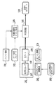
次に、図2を参照して、本発明に係る光信号送信装置の第2の実施の形態を説明する。図2に示す光信号送信装置は、図1におけるレーザ107の代わりに波長可変レーザ201を含み、かつ新たに波長可変レーザ制御装置202と、出力波長制御信号入力ポート203とを含む。その他の構成要素は、第1の実施形態と同じである。
[Second Embodiment]
Next, a second embodiment of the optical signal transmission device according to the present invention will be described with reference to FIG. The optical signal transmission device shown in FIG. 2 includes a wavelength
以上の構成において、波長可変レーザ201として、例えば、半導体のDFBレーザの素子温度を制御することによって出力波長を所望の波長に設定可能としたレーザや、複数の発光波長の異なるDFBレーザの出力を光カプラで結合し、所望の出力波長で発光するDFBレーザのみを駆動することで出力波長を所望の波長に設定可能としたレーザや、電流を注入することにより素子の屈折率を調整し、出力波長を所望の波長に設定可能とした多端子型の半導体レーザ等を使用できる。ただし、これらの波長可変レーザは、本実施形態の機能を実現するために使用可能な装置の一例に過ぎず、同様の機能を実現する他の装置の使用する場合も、本発明に含まれる。
In the above configuration, as the wavelength
本実施形態では、光源101内に波長可変レーザ201を内蔵する。波長可変レーザ201の出力波長は、出力波長制御信号入力ポート203から入力される信号に応じて、波長可変レーザ制御装置202によって制御され、所望の波長に定められるものとする。
In the present embodiment, the wavelength
上記以外の構成は、第1の実施形態と同様であるので、その詳細な説明は省略する。 Since the configuration other than the above is the same as that of the first embodiment, a detailed description thereof will be omitted.
本実施形態では、上記の波長可変レーザ201を使用することにより、バースト通信に用いられる一連のデータを塊として生成した信号を、一連のデータの塊ごとに異なる信号波長で出力することの可能な、光信号送信装置を得ることができる。
In the present embodiment, by using the
なお、特殊な装置を使用することなく、バースト通信に用いる無信号状態を含む光信号を、波形の歪みなく生成することのできる、光信号送信装置を実現できることは、第1の実施形態と同様である。 As in the first embodiment, it is possible to realize an optical signal transmission device that can generate an optical signal including a no-signal state used for burst communication without using waveform distortion without using a special device. It is.
[第3の実施形態]
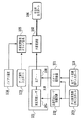
さらに、図3を参照して、本発明に係る光信号送信装置の第3の実施の形態を説明する。図3に示す光信号送信装置は、図2における構成部品の他に、新たに光ゲート制御装置301を含む。その他の構成要素は、第2の実施形態と同じである。
[Third Embodiment]
Furthermore, a third embodiment of the optical signal transmission device according to the present invention will be described with reference to FIG. The optical signal transmission device shown in FIG. 3 newly includes an optical
本実施形態では、波長可変レーザ201の出力レベルが、出力波長ごとにばらついている場合の対応策を示す。波長可変レーザ201の出力波長は、出力波長制御信号入力ポート203から入力される信号(出力波長制御信号)に応じて、波長可変レーザ制御装置202によって制御され、所望の波長に定められる。これと同時に、出力波長制御信号入力ポート203から入力される信号(出力波長制御信号)と、光ゲート制御信号入力ポート108から入力される信号(光ゲート制御信号)は、それぞれ光ゲート制御装置301に入力される。光ゲート制御装置301は、光ゲート制御信号入力ポート108から入力される信号に応じて光ゲート107の透過・遮断を制御し、かつ出力波長制御信号入力ポート203から入力される信号に応じて光ゲート107からの出力レベルを制御することで、所望の出力タイミング・出力レベルで光源101からの出力光を得る。
In this embodiment, a countermeasure is shown when the output level of the wavelength
例えば、光ゲート108としてSOAを利用する場合には、注入電流量で利得を制御するため、光ゲート制御装置301は、光ゲート制御信号入力ポート108から入力される信号に応じた時間の間、出力波長制御信号入力ポート203から入力される信号に応じた電流量を、光ゲート107に注入する。これにより、光ゲート107から所望の出力タイミング・出力レベルで出力光が得られる。
For example, when SOA is used as the
上記以外の構成は、第1、第2の実施形態と同様であるので、その詳細な説明は省略する。 Since the configuration other than the above is the same as that of the first and second embodiments, a detailed description thereof will be omitted.
本実施形態では、以上のような光ゲート制御装置301を使用することにより、バースト通信に用いられる一連のデータを塊として生成した信号を、一連のデータの塊ごとに異なる信号波長で出力することが可能で、かつ出力レベルが均一である、光信号送信装置を得ることができる。
In this embodiment, by using the optical
なお、特殊な装置を使用することなく、バースト通信に用いる無信号状態を含む光信号を、波形の歪みなく生成することのできる、光信号送信装置を実現できることは、第1、第2の実施形態と同様である。 It is to be noted that the first and second embodiments can realize an optical signal transmission device that can generate an optical signal including a no-signal state used for burst communication without using waveform distortion without using a special device. It is the same as the form.
[他の実施の形態]
上記では、本発明の好適な実施形態を例示して説明したが、本発明の実施形態は上記例示に限定されるものではなく、特許請求の範囲に記載の範囲内であれば、その構成部材等の置換、変更、追加、個数の増減、形状の設計変更等の各種変形は、全て本発明の実施形態に含まれる。
[Other embodiments]
In the above, the preferred embodiment of the present invention has been described by way of example. However, the embodiment of the present invention is not limited to the above-described example, and the constituent members thereof are within the scope of the claims. Various modifications such as replacement, change, addition, increase / decrease in number, change in shape design, and the like are all included in the embodiment of the present invention.
101 光源
102 外部変調器
103 電気のデータ信号入力ポート
104 バイアス電源
105 外部変調器用ドライバ回路
106 光信号出力ポート
107 レーザ
108 光ゲート
109 光ゲート制御信号入力ポート
201 波長可変レーザ
202 波長可変レーザ制御装置
203 出力波長制御信号入力ポート
301 光ゲート制御装置
401 光源
402 外部変調器
403 電気のデータ信号入力ポート
404 バイアス電源
405 外部変調器用ドライバ回路
406 光信号出力ポート
DESCRIPTION OF
Claims (5)
前記第1の電気信号とタイミングが取れている第2の電気信号を外部から入力する第2の入力ポートであって、該第2の電気信号は意味あるデータの塊と塊の間に、データ信号速度と同程度の速度の信号を挿入して低周波の信号成分を削除した信号である、第2の入力ポートと、
光信号を発生する光源であって、前記第1の電気信号によって該光信号の透過/遮断を切り換える光ゲートを内部に有する光源と、
前記光源からの入力光信号の透過/遮断を前記第2の電気信号による入力電圧に応じて切り換える外部変調器と、
前記外部変調器から出力される光信号を装置からの出力信号として外部に出力する出力ポートと、
を具備することを特徴とする光信号送信装置。 A first input port for inputting a first electrical signal from the outside;
A second input port for inputting a second electrical signal, which is timed with the first electrical signal, from the outside, wherein the second electrical signal is a data block between meaningful chunks of data; A second input port, which is a signal obtained by inserting a signal having a speed similar to the signal speed and deleting a low-frequency signal component;
A light source that generates an optical signal, the optical source having an optical gate that switches between transmission and blocking of the optical signal by the first electric signal;
An external modulator that switches transmission / cutoff of an input optical signal from the light source in accordance with an input voltage by the second electric signal;
An output port for outputting an optical signal output from the external modulator to the outside as an output signal from the device;
An optical signal transmission device comprising:
5. The light source including the optical gate is integrated as a single unit, or the light source including the optical gate and the external modulator are integrated as a single unit. The optical signal transmission device described.
Priority Applications (1)
| Application Number | Priority Date | Filing Date | Title |
|---|---|---|---|
| JP2006014041A JP2007201540A (en) | 2006-01-23 | 2006-01-23 | Optical signal transmitter |
Applications Claiming Priority (1)
| Application Number | Priority Date | Filing Date | Title |
|---|---|---|---|
| JP2006014041A JP2007201540A (en) | 2006-01-23 | 2006-01-23 | Optical signal transmitter |
Publications (1)
| Publication Number | Publication Date |
|---|---|
| JP2007201540A true JP2007201540A (en) | 2007-08-09 |
Family
ID=38455715
Family Applications (1)
| Application Number | Title | Priority Date | Filing Date |
|---|---|---|---|
| JP2006014041A Pending JP2007201540A (en) | 2006-01-23 | 2006-01-23 | Optical signal transmitter |
Country Status (1)
| Country | Link |
|---|---|
| JP (1) | JP2007201540A (en) |
Cited By (4)
| Publication number | Priority date | Publication date | Assignee | Title |
|---|---|---|---|---|
| JP2010283644A (en) * | 2009-06-05 | 2010-12-16 | Nippon Telegr & Teleph Corp <Ntt> | Optical access network, optical communication method, and optical subscriber device |
| JP2014138195A (en) * | 2013-01-15 | 2014-07-28 | Nippon Telegr & Teleph Corp <Ntt> | Wavelength-tunable burst transmitter |
| WO2014208529A1 (en) * | 2013-06-27 | 2014-12-31 | 日本電信電話株式会社 | Burst optical signal transmission device and control method for burst optical signal transmission device |
| US10819377B1 (en) | 2019-05-03 | 2020-10-27 | Raytheon Company | Radio frequency to optical transmitter |
-
2006
- 2006-01-23 JP JP2006014041A patent/JP2007201540A/en active Pending
Cited By (9)
| Publication number | Priority date | Publication date | Assignee | Title |
|---|---|---|---|---|
| JP2010283644A (en) * | 2009-06-05 | 2010-12-16 | Nippon Telegr & Teleph Corp <Ntt> | Optical access network, optical communication method, and optical subscriber device |
| JP2014138195A (en) * | 2013-01-15 | 2014-07-28 | Nippon Telegr & Teleph Corp <Ntt> | Wavelength-tunable burst transmitter |
| WO2014208529A1 (en) * | 2013-06-27 | 2014-12-31 | 日本電信電話株式会社 | Burst optical signal transmission device and control method for burst optical signal transmission device |
| JP2015011124A (en) * | 2013-06-27 | 2015-01-19 | 日本電信電話株式会社 | Burst light signal transmission device, and control method of the same |
| CN105324703A (en) * | 2013-06-27 | 2016-02-10 | 日本电信电话株式会社 | Burst optical signal transmission device and control method for burst optical signal transmission device |
| US20160127045A1 (en) * | 2013-06-27 | 2016-05-05 | Nippon Telegraph And Telephone Corporation | Burst optical signal transmission device and control method for burst optical signal transmission device |
| US9923637B2 (en) | 2013-06-27 | 2018-03-20 | Nippon Telegraph And Telephone Corporation | Burst optical signal transmission device and control method for burst optical signal transmission device |
| US10819377B1 (en) | 2019-05-03 | 2020-10-27 | Raytheon Company | Radio frequency to optical transmitter |
| WO2020226728A3 (en) * | 2019-05-03 | 2020-12-17 | Raytheon Company | Radio frequency to optical transmitter |
Similar Documents
| Publication | Publication Date | Title |
|---|---|---|
| EP2858273B1 (en) | Light quantum phase modulating system | |
| EP3349376B1 (en) | Pam4 signal generation apparatus | |
| US20140199075A1 (en) | Apparatus and method for controlling multicarrier light source generator | |
| US10680399B2 (en) | Optical module | |
| JP4532367B2 (en) | Optical transmission apparatus and method using frequency shift keying | |
| US20170093116A1 (en) | Optical module | |
| JP2005073262A (en) | Duobinary optical transmission device using semiconductor optical amplifier, and duobinary optical transmission method | |
| CN107408987B (en) | Pluggable optical module, optical communication system and pluggable optical module control method | |
| CN106921439A (en) | A kind of optical module | |
| JP2007201540A (en) | Optical signal transmitter | |
| US20020171903A1 (en) | Return-to-zero optical modulator with configurable pulse width | |
| JP2011501618A (en) | Light to millimeter wave conversion | |
| JP2004343766A (en) | Duobinary optical transmission apparatus using semiconductor optical amplifier | |
| JP2005173614A (en) | Method and apparatus for multi-band optical switching using multi-pump parametric device | |
| CN102792614A (en) | Dual drive externally modulated laser | |
| JP2007114307A (en) | Chirp-switching circuit and optical transmission system | |
| US20150331262A1 (en) | Optical modulator, optical transmitter, optical transmission/reception system, and control method for optical modulator | |
| JP2000162561A (en) | Light subcarrier phase modulator and optical spectrum spread transmitter using same | |
| KR101880367B1 (en) | Method and apparatus for generating complex format optical signal using direct modulation of optical injection-locked semiconductor laser | |
| KR102557191B1 (en) | Optical transmitter based on optical time division multiplexing | |
| JP5646673B2 (en) | Optical packet signal generator | |
| EP1422842B1 (en) | Duobinary optical transmission apparatus | |
| CN102778801B (en) | Normal-phase/inverse-phase all-optical wavelength conversion device | |
| US20220360339A1 (en) | Optical transmitter based on optical time division multiplexing | |
| CN103297016B (en) | Optical transmitter and optical communication method |