JP2007200577A - Lighting device and liquid crystal display device - Google Patents
Lighting device and liquid crystal display device Download PDFInfo
- Publication number
- JP2007200577A JP2007200577A JP2006014406A JP2006014406A JP2007200577A JP 2007200577 A JP2007200577 A JP 2007200577A JP 2006014406 A JP2006014406 A JP 2006014406A JP 2006014406 A JP2006014406 A JP 2006014406A JP 2007200577 A JP2007200577 A JP 2007200577A
- Authority
- JP
- Japan
- Prior art keywords
- light emitting
- emitting element
- light
- current
- lighting device
- Prior art date
- Legal status (The legal status is an assumption and is not a legal conclusion. Google has not performed a legal analysis and makes no representation as to the accuracy of the status listed.)
- Pending
Links
Images


Landscapes
- Design And Manufacture Of Integrated Circuits (AREA)
- Led Devices (AREA)
- Liquid Crystal (AREA)
- Circuit Arrangement For Electric Light Sources In General (AREA)
Abstract
Description
本発明は、照明装置、およびこの照明装置を備える液晶表示装置に関する。 The present invention relates to a lighting device and a liquid crystal display device including the lighting device.
透過型および半透過型の液晶表示装置は、液晶表示パネルと、この液晶表示パネルの背面に設けられるバックライトとを含んで構成される。バックライトは、液晶表示装置の視認性を高めるために液晶表示パネルに光を照射する照明装置として用いられる。このバックライトには、冷陰極蛍光灯(Cold Cathode Fluorescent Lamp:略称CCFL)が広く用いられている。冷陰極蛍光灯は、外形が大きいので、バックライトの小形化が困難である。また冷陰極蛍光灯を駆動する駆動回路に、昇圧回路および安定器などを必要とするので、バックライトの構成が複雑になるという問題がある。この問題を解決するために、冷陰極蛍光灯と比べて小形化が容易で、かつ駆動回路に昇圧回路および安定器などを必要としない発光ダイオード(Light Emitting Diode:略称LED)を用いた照明装置が、バックライトとして提案されている。 The transmissive and transflective liquid crystal display devices include a liquid crystal display panel and a backlight provided on the back surface of the liquid crystal display panel. The backlight is used as an illumination device that irradiates light to the liquid crystal display panel in order to improve the visibility of the liquid crystal display device. As this backlight, a cold cathode fluorescent lamp (abbreviated as CCFL) is widely used. Since the cold cathode fluorescent lamp has a large outer shape, it is difficult to reduce the size of the backlight. Further, since a drive circuit for driving the cold cathode fluorescent lamp requires a booster circuit and a ballast, there is a problem that the configuration of the backlight becomes complicated. In order to solve this problem, an illumination device using a light emitting diode (abbreviated as LED), which is easy to downsize as compared with a cold cathode fluorescent lamp and does not require a booster circuit or a ballast in a drive circuit. Has been proposed as a backlight.
従来の照明装置として、複数のLEDが直列に接続されて構成される照明装置がある。この照明装置は、複数のLEDが並列に接続されて構成される照明装置に比べて、LEDの内部抵抗を合成した合成抵抗が大きくなるので、回路に流れる電流が小さくなり、照明装置の消費電力を小さくすることができる。しかし、LEDは、寿命および故障などによって発光しなくなると、通常、電気的に非導通、すなわちオープンモードとなるので、LEDが1つでもオープンモードになった場合に、全てのLEDが発光しなくなるという問題がある。 As a conventional lighting device, there is a lighting device configured by connecting a plurality of LEDs in series. Compared to a lighting device configured by connecting a plurality of LEDs in parallel, this lighting device has a larger combined resistance, which is a combination of the internal resistances of the LEDs, so the current flowing through the circuit is reduced and the power consumption of the lighting device is reduced. Can be reduced. However, when an LED ceases to emit light due to its lifespan or failure, it is normally electrically non-conductive, that is, an open mode. Therefore, when even one LED enters an open mode, all LEDs do not emit light. There is a problem.
また従来の照明装置として、複数のLEDが並列に接続されて構成される照明装置がある。この照明装置は、1つのLEDがオープンモードになった場合でも、オープンモードになったLEDを除く残余のLEDは、発光状態を維持する。しかし、LEDを並列に接続した場合、電流源から各LEDに流れる電流の合計の電流を供給する必要があり、電流源から流れる電流が大きくなるので、途中の配線部で消費される電力が大きくなるという問題がある。 As a conventional lighting device, there is a lighting device configured by connecting a plurality of LEDs in parallel. In this lighting device, even when one LED is in the open mode, the remaining LEDs except for the LED in the open mode maintain the light emitting state. However, when the LEDs are connected in parallel, it is necessary to supply the total current flowing from the current source to each LED, and the current flowing from the current source increases, so that the power consumed in the intermediate wiring section is large. There is a problem of becoming.
以上述べた複数のLEDが直列または並列に接続されて構成される照明装置の問題点を解決するために、直列接続と並列接続とを併用した照明装置がある。 In order to solve the problems of the lighting device configured by connecting the plurality of LEDs described above in series or in parallel, there is a lighting device using both serial connection and parallel connection.
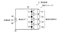
図16は、第1の従来の技術の照明装置1の回路構成を示す回路図である。この照明装置1は、第1直列発光素子アレイ2と第2直列発光素子アレイ3と定電流源4とを含んで構成される。
FIG. 16 is a circuit diagram showing a circuit configuration of the illumination device 1 of the first conventional technique. The lighting device 1 includes a first series light emitting element array 2, a second series light emitting element array 3, and a constant
第1直列発光素子アレイ2は、4つのLED5a〜5dが直列に接続されて構成される。第2直列発光素子アレイ3は、4つのLED6a〜6dが直列に接続されて構成される。第1直列発光素子アレイ2と第2直列発光素子アレイ3とは、並列に接続される。定電流源4は、第1直列発光素子アレイ2と第2直列発光素子アレイ3とに接続され、第1直列発光素子アレイ2と第2直列発光素子アレイ3とに定電流を供給する。
The first series light emitting element array 2 is configured by connecting four
たとえば第1直列発光素子アレイ2の1つのLED5aがオープンモードになると、他の3つのLED5b,5c,5dに電流が流れなくなり、第1直列発光素子アレイ2の全てのLEDが消灯するが、第2直列発光素子アレイ3の4つのLED6a〜6dは、発光状態を維持するので、照明装置1を構成する全てのLEDが消灯することを防ぐことができる。特に第1直列発光素子アレイ2のLED5a〜5dと第2直列発光素子アレイ3のLED6a〜6dとを交互に直線状に並べて配置することによって、照明装置6の輝度むらを分散することができる(たとえば特許文献1参照)。
For example, when one
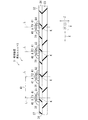
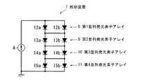
図17は、第2の従来の技術の照明装置7の回路構成を示す回路図である。この照明装置7は、第1〜第4並列発光素子アレイ8〜11と、定電流源4とを含んで構成される。
FIG. 17 is a circuit diagram showing a circuit configuration of the illumination device 7 of the second conventional technique. The illumination device 7 includes first to fourth parallel light emitting element arrays 8 to 11 and a constant
第1並列発光素子アレイ8は、2つのLED12a,12bが並列に接続されて構成される。第2並列発光素子アレイ9は、2つのLED13a,13bが並列に接続されて構成される。第3並列発光素子アレイ10は、2つのLED14a,14bが並列に接続されて構成される。第4並列発光素子アレイ11は、2つのLED15a,15bが並列に接続されて構成される。第1〜第4並列発光素子アレイ8〜11は、それぞれ直列に接続される。定電流源4は、第1並列発光素子アレイ8と第4並列発光素子アレイ11とに接続され、第1〜第4並列発光素子アレイ8〜11に定電流を供給する。
The first parallel light-emitting element array 8 is configured by connecting two
各第1〜第4並列発光素子アレイ8〜11の2つのLEDのうちの一方が、故障または寿命によってオープンモードになったとしても、他方のLEDが発光状態を保つので、オープンモードになったLEDを除く残余のLEDは、発光し、照明装置7の輝度むらを最小限に抑えることができる。 Even if one of the two LEDs of each of the first to fourth parallel light-emitting element arrays 8 to 11 is in the open mode due to a failure or a lifetime, the other LED is kept in the light emitting state, so that it is in the open mode. The remaining LEDs other than the LEDs emit light, and the luminance unevenness of the illumination device 7 can be minimized.
第1の従来の技術の照明装置1では、1つのLEDがオープンモードになると、オープンモードになったLEDが含まれる直列発光素子アレイの全てのLEDが発光しなくなる。 In the lighting device 1 of the first conventional technique, when one LED enters the open mode, all the LEDs in the series light emitting element array including the LEDs in the open mode do not emit light.
大型の液晶表示パネルの照明装置は、1000個程度のLEDを含んで構成され、各直列発光素子アレイは、25個から30個のLEDが直列に接続されて構成される。したがって、1つのLEDがオープンモードになると、25個から30個のLEDが消灯し、液晶表示パネルに輝度むらが生じる。LEDの寿命にはばらつきがあるので、早期に寿命を迎えて消灯するLEDがあり、早期に25個から30個のLEDが消灯して液晶表示パネルに輝度むらが生じることがある。 The lighting device for a large liquid crystal display panel is configured to include about 1000 LEDs, and each series light emitting element array is configured by connecting 25 to 30 LEDs in series. Therefore, when one LED is in the open mode, 25 to 30 LEDs are turned off, resulting in uneven brightness in the liquid crystal display panel. Since there are variations in the life of LEDs, there are LEDs that reach the end of their life and turn off at an early stage, and from 25 to 30 LEDs turn off at an early stage, resulting in uneven brightness in the liquid crystal display panel.
第2の従来の技術の照明装置7は、各発光素子アレイの2つのLEDのうちの一方のLEDがオープンモードになったとしても、他方のLEDは発光状態を維持する。このとき、他方のLEDに全電流が流れて、他方のLEDに流れる電流が2倍になるので、輝度が高くなり、輝度むらが生じる。したがって、一方のLEDがオープンモードになると、他方のLEDが早期に寿命を迎えてオープンモードになる可能性が高くなる。並列発光素子アレイの両方のLEDがオープンモードになると、この並列発光素子アレイに直列に接続された全ての並列発光素子アレイのLEDが消灯するという問題がある。 In the illumination device 7 of the second conventional technique, even if one of the two LEDs in each light emitting element array is in the open mode, the other LED maintains the light emitting state. At this time, since the entire current flows through the other LED and the current flowing through the other LED doubles, the luminance increases and luminance unevenness occurs. Therefore, when one LED enters the open mode, there is a high possibility that the other LED will reach the end of its life and enter the open mode. When both LEDs of the parallel light emitting element array are in the open mode, there is a problem in that the LEDs of all the parallel light emitting element arrays connected in series to the parallel light emitting element array are turned off.
したがって本発明の目的は、輝度むらの発生を抑制することができる照明装置および液晶表示装置を提供することである。 Accordingly, an object of the present invention is to provide an illumination device and a liquid crystal display device that can suppress the occurrence of uneven brightness.
本発明は、相互に直列に接続され、電圧を印加することによって発光する複数の発光素子と、
前記直列に接続される複数の発光素子に直列に接続され、各発光素子に電力を供給する電源部と、
各発光素子に個別に並列に接続され、各発光素子が発光状態のときに印加される電圧よりも高い予め定める電圧が印加されたときに、電流が流れない非導通状態から電流が流れる導通状態に変化する複数の電流迂回素子とを含むことを特徴とする照明装置である。
The present invention includes a plurality of light emitting elements connected in series to each other and emitting light by applying a voltage;
A power supply unit connected in series to the plurality of light emitting elements connected in series and supplying power to each light emitting element;
A conductive state in which a current flows from a non-conductive state where no current flows when a predetermined voltage higher than the voltage applied when each light emitting element is in a light emitting state is applied in parallel to each light emitting element. And a plurality of current diverting elements that change to a lighting device.
本発明に従えば、発光素子が正常で発光可能な状態とき、この発光素子は、電源部から電力を供給されて発光する発光状態となる。各発光素子は、電流迂回素子が個別に並列に接続されるので、発光素子が発光状態のときには、この発光素子に印加される電圧と同じ電圧が印加される。複数の発光素子のうちのいずれかが故障などによって消灯状態となり、電流が流れない非導通状態に変化すると、この変化した発光素子に並列に接続された電流迂回素子には、非導通状態に変化した発光素子を除く残余の発光素子に印加されていた電圧を合計した電圧が一時的に印加される。この電圧が予め定める電圧よりも高くなると、電流迂回素子は、非導通状態から電流が流れる導通状態に変化する。つまり各電流迂回素子は、並列に接続された発光素子が非導通状態に変化すると、導通状態に変化する。 According to the present invention, when the light emitting element is normal and capable of emitting light, the light emitting element is in a light emitting state in which power is supplied from the power supply unit to emit light. Since each light-emitting element is individually connected in parallel with a current bypass element, when the light-emitting element is in a light-emitting state, the same voltage as that applied to the light-emitting element is applied. If one of the light emitting elements is turned off due to a failure or the like and changes to a non-conductive state where no current flows, the current bypass element connected in parallel to the changed light emitting element changes to a non-conductive state. A voltage obtained by adding up the voltages applied to the remaining light emitting elements excluding the light emitting elements is temporarily applied. When this voltage becomes higher than a predetermined voltage, the current bypass element changes from a non-conductive state to a conductive state in which a current flows. That is, each current bypass element changes to a conductive state when a light emitting element connected in parallel changes to a non-conductive state.
発光素子が寿命または故障によって非導通状態に変化したとしても、この発光素子に流れていた電流は、並列に接続された電流迂回素子を迂回して流れるようになる。したがって、直列に接続された複数の発光素子のうちのいずれかの発光素子が非導通状態となったとしても、非導通状態となった発光素子を除く残余の発光素子は、導通状態を保ち、発光し続ける。これによって、複数の発光素子を直列に接続した構成を有する照明装置であっても、発光素子のうちの非導通状態に変化した発光素子のみが消灯し、正常な発光素子は発光状態を維持する。 Even if the light emitting element changes to a non-conducting state due to the life or failure, the current flowing in the light emitting element flows around the current bypass element connected in parallel. Therefore, even if any one of the plurality of light emitting elements connected in series becomes non-conductive, the remaining light emitting elements other than the non-conductive light emitting elements remain conductive, Continue to emit light. As a result, even in a lighting device having a configuration in which a plurality of light emitting elements are connected in series, only the light emitting elements that have changed to a non-conductive state among the light emitting elements are turned off, and the normal light emitting elements maintain the light emitting state. .
また電流迂回素子は、印加する電圧によって非導通状態から導通状態に変化する単純な機能で実現されるので、電流迂回素子の作成が容易になる。 In addition, since the current bypass element is realized by a simple function that changes from a non-conductive state to a conductive state depending on the applied voltage, it is easy to create the current bypass element.
また発光素子を直列に接続するので、各発光素子の同じ電流を流し、同じ電圧を加え、輝度が同じになるように構成した場合、並列に接続する場合に比べて、電源付近に流れる電流は小さくなるので、銅損が小さくなり、配線を細くすることができるため、回路の配線が煩雑とならない。 In addition, since the light emitting elements are connected in series, when the same current is applied to each light emitting element, the same voltage is applied, and the luminance is the same, the current flowing near the power supply is less than when connected in parallel. Since the copper loss is reduced and the wiring can be thinned, the wiring of the circuit is not complicated.
また本発明は、前記電源部は、定電流を前記複数の発光素子に供給する定電流源から成り、
前記電流迂回素子は、前記予め定める電圧が印加されたときに、非導通状態から導通状態に遷移することを特徴とする。
In the present invention, the power supply unit includes a constant current source that supplies a constant current to the plurality of light emitting elements.
The current bypass element transitions from a non-conduction state to a conduction state when the predetermined voltage is applied.
また電源部は、定電流源から成るので、発光素子が非導通状態になり、電流迂回素子が導通状態に変化しても、発光状態の各発光素子に流れる電流の大きさは変化せず、各発光素子に印加される電圧は、変化しない。すなわち導通状態の発光素子の消費電力が変化しない。したがって、いずれかの発光素子が非導通状態に変化しても、導通状態の発光素子に過負荷がかからず、導通状態の発光素子の寿命を縮めることを抑制することができる。 In addition, since the power supply unit is composed of a constant current source, even if the light emitting element becomes non-conductive and the current bypass element changes to the conductive state, the magnitude of the current flowing through each light emitting element in the light emitting state does not change, The voltage applied to each light emitting element does not change. That is, the power consumption of the light emitting element in the conductive state does not change. Therefore, even when any of the light-emitting elements changes to a non-conductive state, the conductive light-emitting element is not overloaded, and the lifetime of the conductive light-emitting element can be suppressed from being shortened.
また電流迂回素子は、前記予め定める電圧が印加されたときに、非導通状態から導通状態に遷移するので、発光素子が非導通状態から導通状態に戻ったとしても、導通状態を維持する。導通状態の電流迂回素子にはほとんど電圧が印加されないので、導通状態の電流迂回素子に並列に接続された発光素子が導通状態に戻ったとしても、この発光素子は、ほとんど電圧が印加されず、発光しない。 The current bypass element transitions from the non-conducting state to the conducting state when the predetermined voltage is applied. Therefore, even if the light emitting element returns from the non-conducting state to the conducting state, the current bypassing element maintains the conducting state. Since almost no voltage is applied to the conductive current bypass element, even if the light emitting element connected in parallel to the conductive current bypass element returns to the conductive state, this light emitting element receives almost no voltage, Does not emit light.
また本発明は、前記発光素子は、発光ダイオードから成ることを特徴とする。
本発明に従えば、発光素子は、電流の変動に対して順方向電圧降下の変動が小さい発光ダイオードから成るので、各発光素子に印加される電圧の変動を抑制することができる。したがって発光素子が発光状態のときの発光素子に印加される電圧が予め定める電圧を超えることを防ぐことができ、この発光素子に並列に接続された電流迂回素子が導通状態に変化することを防ぐことができる。
In the invention, it is preferable that the light emitting element is a light emitting diode.
According to the present invention, since the light emitting element is composed of a light emitting diode having a small forward voltage drop variation with respect to a current variation, it is possible to suppress variations in the voltage applied to each light emitting element. Therefore, the voltage applied to the light emitting element when the light emitting element is in the light emitting state can be prevented from exceeding a predetermined voltage, and the current bypassing element connected in parallel to the light emitting element is prevented from changing to the conductive state. be able to.
また発光ダイオードに流れる電流の大きさを調整するだけで発光輝度を調整することができるので、駆動回路に昇圧回路および安定器などを必要とする冷陰極蛍光灯を用いた照明装置に比べて、照明装置の構成が簡易となる。また発光ダイオードのサイズは、冷陰極蛍光灯のサイズに比べて非常に小さいので、照明装置の小形化が実現される。 In addition, since it is possible to adjust the light emission brightness simply by adjusting the magnitude of the current flowing through the light emitting diode, compared to a lighting device using a cold cathode fluorescent lamp that requires a booster circuit and a ballast in the drive circuit, The configuration of the lighting device is simplified. Further, since the size of the light emitting diode is very small compared to the size of the cold cathode fluorescent lamp, the size of the lighting device can be reduced.
また本発明は、液晶表示パネルと、
液晶表示パネルの厚み方向の一表面に対向して設けられる前記照明装置とを含むことを特徴とする液晶表示装置である。
The present invention also provides a liquid crystal display panel;
A liquid crystal display device comprising: the lighting device provided to face one surface in the thickness direction of the liquid crystal display panel.
本発明に従えば、発光素子のうちの寿命または故障によって非導通状態に変化した発光素子のみが消灯する照明装置からの光が、液晶表示パネルに照射される。 According to the present invention, the light from the lighting device that turns off only the light emitting element that has changed to the non-conducting state due to the lifetime or failure of the light emitting elements is irradiated to the liquid crystal display panel.
本発明によれば、複数の発光素子を直列に接続した構成を有する照明装置であっても、発光素子のうちの寿命または故障によって非導通状態に変化した発光素子のみが消灯し、正常な発光素子は発光状態を維持する。寿命または故障によって非導通状態に変化した発光素子が、他の発光素子に影響を与えて他の発光素子が消灯することを防ぐことができるので、照明装置の輝度むらの発生を抑制することができる。 According to the present invention, even in a lighting device having a configuration in which a plurality of light-emitting elements are connected in series, only the light-emitting elements that have changed to a non-conductive state due to the life or failure of the light-emitting elements are turned off and normal light emission is performed. The element maintains a light emitting state. A light emitting element that has changed to a non-conducting state due to a life or failure can prevent other light emitting elements from being turned off by affecting other light emitting elements, thereby suppressing unevenness in luminance of the lighting device. it can.
また電流迂回素子は、印加する電圧によって非導通状態から導通状態に変化する単純な機能で実現されるので、電流迂回素子の作成が容易になる。 In addition, since the current bypass element is realized by a simple function that changes from a non-conductive state to a conductive state depending on the applied voltage, it is easy to create the current bypass element.
また発光素子を直列に接続するので、並列に接続する場合に比べて、各発光素子の内部抵抗を合成した回路の合成抵抗が大きくなり、回路に流れる電流が小さくなるので、消費電力を小さくすることができる。 In addition, since the light emitting elements are connected in series, the combined resistance of the circuit in which the internal resistances of the respective light emitting elements are combined is increased and the current flowing in the circuit is reduced, so that the power consumption is reduced. be able to.
また、非導通状態になる発光素子が生じても、導通状態の発光素子に過負荷がかからないので、導通状態の発光素子の寿命を縮めることを抑制することができ、寿命の長い照明装置を実現することができる。 In addition, even if a light-emitting element that is in a non-conducting state is generated, an overload is not applied to the light-emitting element that is in a conductive state. can do.
また電流迂回素子は、前記予め定める電圧が印加されたときに、非導通状態から導通状態に遷移するので、発光素子が非導通状態から導通状態に戻ったとしても、導通状態を維持する。導通状態の電流迂回素子にはほとんど電圧が印加されないので、導通状態の電流迂回素子に並列に接続された発光素子が導通状態に戻ったとしても、この発光素子は、ほとんど電圧が印加されず、発光しない。これによって発光素子が点滅することを防ぐことができる。 The current bypass element transitions from the non-conducting state to the conducting state when the predetermined voltage is applied. Therefore, even if the light emitting element returns from the non-conducting state to the conducting state, the current bypassing element maintains the conducting state. Since almost no voltage is applied to the conductive current bypass element, even if the light emitting element connected in parallel to the conductive current bypass element returns to the conductive state, this light emitting element receives almost no voltage, Does not emit light. This can prevent the light emitting element from blinking.
また本発明によれば、発光素子は、電流の変動に対して順方向電圧降下の変動が小さい発光ダイオードから成るので、各発光素子に印加される電圧の変動を抑制することができる。したがって発光素子が発光状態のときの発光素子に印加される電圧が予め定める電圧を超えることを防ぐことができ、この発光素子に並列に接続された電流迂回素子が導通状態に変化することを防ぐことができる。これによって発光素子が正常に発光することができる状態にあるにも拘わらず、消灯することを防ぐことができ、照明装置の輝度むらの発生を抑制することができる。 Further, according to the present invention, the light emitting element is composed of a light emitting diode having a small forward voltage drop fluctuation with respect to a current fluctuation, and therefore fluctuations in the voltage applied to each light emitting element can be suppressed. Therefore, the voltage applied to the light emitting element when the light emitting element is in the light emitting state can be prevented from exceeding a predetermined voltage, and the current bypass element connected in parallel to the light emitting element is prevented from changing to the conductive state. be able to. Accordingly, it is possible to prevent the light emitting element from being turned off despite being in a state where the light emitting element can emit light normally, and it is possible to suppress the occurrence of luminance unevenness of the lighting device.
また発光ダイオードに流れる電流の大きさを調整するだけで発光輝度を調整することができるので、駆動回路に昇圧回路および安定器などを必要とする冷陰極蛍光灯を用いた照明装置に比べて、照明装置の構成が簡易となる。また発光ダイオードのサイズは、冷陰極蛍光灯のサイズに比べて非常に小さいので、照明装置の小形化が実現される。 In addition, since it is possible to adjust the light emission brightness simply by adjusting the magnitude of the current flowing through the light emitting diode, compared to a lighting device using a cold cathode fluorescent lamp that requires a booster circuit and a ballast in the drive circuit, The configuration of the lighting device is simplified. Further, since the size of the light emitting diode is very small compared to the size of the cold cathode fluorescent lamp, the size of the lighting device can be reduced.
また本発明によれば、発光素子のうちの寿命または故障によって非導通状態に変化した発光素子のみが消灯し、輝度むらの発生が抑制された照明装置からの光が、液晶表示パネルに照射される。これによって、輝度むら発生が抑制された液晶表示装置が実現される。 In addition, according to the present invention, only the light emitting element that has changed to a non-conducting state due to the life or failure of the light emitting element is turned off, and the light from the lighting device in which the occurrence of luminance unevenness is suppressed is applied to the liquid crystal display panel. The Thereby, a liquid crystal display device in which the occurrence of luminance unevenness is suppressed is realized.
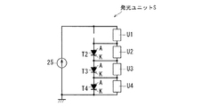
図1は、本発明の実施の一形態の照明装置21の一部の回路構成を示す回路図である。図2は、照明装置21を模式的に表す斜視図である。図3は、照明装置21を模式的に表す断面図である。照明装置21は、液晶表示装置22におけるバックライトとして用いられる。照明装置21は、m(記号mは、正の整数)個の発光ユニットS1,S2,…,Sm−1,Smと、取り付け基板23と、プリント配線基板24とを含んで構成される。各発光ユニットS1,S2,…,Sm−1,Smは、それぞれn(記号nは、2以上の整数)個の発光素子T1,T2,…,Tn−1,Tnと、n個の電流迂回素子U1,U2,…,Un−1,Unと、定電流供給部である定電流源25とを含んで構成される。複数の発光ユニットS1,S2,…,Sm−1,Sm、発光素子T1,T2,…,Tn−1,Tn、電流迂回素子U1,U2,…,Un−1,Unをそれぞれ総称して示す場合、およびそれぞれ不特定のものを示す場合には、単に発光ユニットS、発光素子T、電流迂回素子Uと記載する場合がある。
FIG. 1 is a circuit diagram showing a partial circuit configuration of a lighting device 21 according to an embodiment of the present invention. FIG. 2 is a perspective view schematically showing the lighting device 21. FIG. 3 is a cross-sectional view schematically showing the lighting device 21. The illumination device 21 is used as a backlight in the liquid crystal display device 22. The illumination device 21 includes m (symbol m is a positive integer) light emitting units S1, S2,... Sm-1, Sm, a mounting
本実施の形態では、一例として、m=3かつn=4の場合、すなわち発光ユニットSが3つであって、各発光ユニットSに含まれる発光素子Tおよび電流迂回素子Uがそれぞれ4つの場合について説明する。 In the present embodiment, as an example, when m = 3 and n = 4, that is, there are three light emitting units S, and each of the light emitting units T and the current bypass elements U included in each light emitting unit S is four. Will be described.
照明装置21は、取り付け基板23の厚み方向一表面26上にプリント配線基板24が保持されて設けられ、プリント配線基板24の厚み方向一表面27上に発光素子Tおよび電流迂回素子Uが実装され、発光素子Tおよび電流迂回素子Uを外囲する保護部31が設けられて構成される。
The lighting device 21 is provided with a printed
プリント配線基板24の厚み方向の一表面部には、所定のランド32が形成されている。ランド32は、電子部品の取り付けおよび接続に用いられ、導電性を有する導体のパターンから成る。
A
発光素子Tは、列状にプリント配線基板24の厚み方向一表面27上に配置される。本実施の形態では、発光素子T1,T2,…,Tn−1,Tnは、光軸Lが、プリント配線基板24の厚み方向と一致し、光を発する向きがプリント配線基板24と反対側となるように、プリント配線基板24に直線状に配列されて実装される。光発光素子T1,T2,…,Tn−1,Tnは、第1方向Xの一方から他方に向かって、T1,T2,…,Tn−1,Tn−1,Tnの順番に予め定める第1の間隔W1をあけて配列される。第1の間隔W1は、隣接する発光素子Tの光軸L間の距離である。以後、第1方向Xおよび発光素子Tの光軸L方向に垂直な方向を第2方向Yと記載する場合がある。また発光素子Tの光軸L方向を第3方向Zと記載する場合がある。
The light emitting elements T are arranged on the one
図4は、発光素子Tの断面図である。本実施の形態では発光素子Tは、発光ダイオード(Light Emitting Diode:LED)から成り、カソードKと、カソードKの厚み方向一表面33上に積層されるn型半導体層34と、n型半導体層34の厚み方向一表面35上に積層されるp型半導体層36と、p型半導体層36の厚み方向一表面37に積層されるアノードAとを含んで構成される。アノードAとカソードKとは、金属材料および合金材料などの導電性を有する材料によって形成され、具体的には、金(Au)、金とゲルマニウムとの合金(AuGe)、金と亜鉛との合金(AuZn)、ニッケル(Ni)およびアルミニウム(Al)などによって形成される。n型半導体層34およびp型半導体層36は、ガリウム砒素(GaAs)、アルミニウムガリウム砒素(AlGaAs)、窒化ガリウム(GaN)、窒化アルミニウムガリウムインジウム(AlGaInN)、セレン化亜鉛(ZnSe)、およびインジウムガリウムリン(InGaP)などの半導体材料に不純物をドーピングすることによってよって形成される。特に、照明装置21を液晶表示装置22のバックライトに使用する場合には、発光素子Tは、演色性を高めるため光の3原色である赤、緑、青の発光素子を組み合わせて使用するが、n型半導体層34およびp型半導体層36は、発色の色に応じた半導体材料(赤や緑についてはガリウムヒ素、青については窒化ガリウム)に不純物をドーピングすることによって形成される。
FIG. 4 is a cross-sectional view of the light emitting element T. In the present embodiment, the light emitting element T is composed of a light emitting diode (LED), and includes a cathode K, an n-type semiconductor layer 34 stacked on one
発光素子T1,T2,…,Tn−1,Tnは、発光素子Ti(iはn−1以下の正の整数)のアノードAと発光素子Ti+1のカソードKとが接続されるように、T1,T2,…,Tn−1,Tnの順番に配線38を介して相互に直列に接続される。具体的には、発光素子Ti+1のカソードKは、ランド32に直接接続され、発光素子Ti+1のアノードAは、接続されるべき発光素子TiのカソードKが接続されたランド32に導電性を有するワイヤ41を介して接続させる。前記配線38は、ランド32およびワイヤ41を含んで構成される。本実施の形態では、n=4なので、発光素子T1のカソードKと、発光素子T2のアノードAとが接続され、発光素子T2のカソードKと、発光素子T3のアノードAとが接続され、発光素子T3のカソードKと、発光素子T4のアノードAとが接続される。発光素子Tは、順方向に拡散電位以上の電圧が印加されると、ショートモード、すなわち電気的に導通状態となり、発光する。この発光素子Tが寿命または故障などによって壊れ、発光することができなくなると、通常、オープンモード、すなわち電気的に非導通状態となる。したがって発光素子Tが寿命を迎える、または故障して壊れると、発光素子Tは、ショートモードからオープンモードに遷移する。発光素子Tは、直列に接続されるので、並列に接続される場合に比べて、各発光素子Tの内部抵抗を合成した回路の合成抵抗が大きくなり、回路に流れる電流が小さくなるので、消費電力を小さくすることができる。
The light emitting elements T1, T2,..., Tn−1, Tn are arranged such that the anode A of the light emitting element Ti (i is a positive integer equal to or less than n−1) and the cathode K of the light emitting element Ti + 1 are connected. T2,..., Tn-1, and Tn are connected in series with each other via the
発光素子Tは、定電流源25から電流が供給されることによって発光する。LEDは、流れる電流の大きさによって輝度が変わるが、発光しているときの順方向電圧降下V1は、電流の変動に比べて変動が少ない。したがって、発光状態の発光素子Tに印加される順方向電圧降下V1は、供給される電流が変動しても、ほとんど変動しない。また発光素子Tに流れる電流の大きさを調整するだけで発光輝度を調整することができるので、駆動回路に昇圧回路および安定器などを必要とする冷陰極蛍光灯を用いた照明装置に比べて、照明装置21の構成が簡易となる。またLEDのサイズは、冷陰極蛍光灯のサイズに比べて非常に小さいので、照明装置21の小形化が実現される。
The light emitting element T emits light when current is supplied from the constant
発光ユニットS1,S2,…,Sm−1,Smは、列状に配置され、本実施の形態では第2方向Yに同じ数字の発光素子Tが直線状に並ぶように配列される。発光ユニットS1,S2,…,Sm−1,Smは、第2方向Yの一方から他方に向かってS1,S2,…,Sm−1,Smの順番に予め定める第2の間隔W2をあけて配列される。第2の間隔W2は、隣接する発光ユニットSの同じ番号の発光素子Tの光軸L間の距離である。本実施の形態では、m=3なので、第2方向Yの一方から他方に、発光ユニットS1、発光ユニットS2、発光ユニットS3の順番に配列される。本実施の形態では、発光素子Tは、m×nのマトリックス状に配列される。 The light emitting units S1, S2,..., Sm-1, Sm are arranged in a line, and in the present embodiment, the light emitting elements T having the same numbers are arranged in a straight line in the second direction Y. The light emitting units S1, S2,..., Sm-1, Sm are spaced apart from each other in the order of S1, S2,. Arranged. The second interval W2 is a distance between the optical axes L of the light emitting elements T having the same number in the adjacent light emitting units S. In the present embodiment, since m = 3, the light emitting unit S1, the light emitting unit S2, and the light emitting unit S3 are arranged in this order from one to the other in the second direction Y. In the present embodiment, the light emitting elements T are arranged in an m × n matrix.
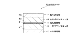
図5は、電流迂回素子Uの構成を模式的に示す断面図である。本実施の形態では、電流迂回素子Uは、アンチヒューズから成り、一方導電層42と、他方導電層43と、一方ポリシリコン層44と、他方ポリシリコン層45と、電気絶縁層46とを含んで構成される。一方導電層42および他方導電層43は、金属材料および合金材料などの導電性を有する材料によって形成され、具体的には、金(Au)、金とゲルマニウムとの合金(AuGe)、金と亜鉛との合金(AuZn)、ニッケル(Ni)およびアルミニウム(Al)などによって形成される。一方ポリシリコン層44および他方ポリシリコン層45は、導電性を有するポリシリコンから成る。電気絶縁層46は、電気絶縁性を有し、酸化シリコン(SiO2)などによって形成される。電流迂回素子Uは、一方導電層42の厚み方向一表面47に、一方ポリシリコン層44が積層され、一方ポリシリコン層44の厚み方向一表面51に電気絶縁層46が積層され、電気絶縁層46の厚み方向一表面52に他方ポリシリコン層45が積層され、他方ポリシリコン層45の厚み方向一表面53に他方導電層43が積層されて構成される。電流迂回素子Uは、半導体プロセスによって小形に形成される。このような小形の電流迂回素子Uを用いることによって、照明装置21の小形化が実現される。
FIG. 5 is a cross-sectional view schematically showing the configuration of the current bypass element U. In the present embodiment, the current bypass element U is made of an antifuse, and includes one conductive layer 42, the other conductive layer 43, one polysilicon layer 44, the other polysilicon layer 45, and an electrical insulating layer 46. Consists of. On the other hand, the conductive layer 42 and the other conductive layer 43 are formed of a conductive material such as a metal material and an alloy material. Specifically, gold (Au), an alloy of gold and germanium (AuGe), gold and zinc Alloy (AuZn), nickel (Ni), aluminum (Al), and the like. On the other hand, the polysilicon layer 44 and the other polysilicon layer 45 are made of conductive polysilicon. The electrical insulating layer 46 has electrical insulation and is formed of silicon oxide (SiO 2 ) or the like. In the current bypass element U, one polysilicon layer 44 is laminated on one
電流迂回素子U1,U2,…,Un−1,Unは、配線38を介して各発光素子T1,T2,…,Tn−1,Tnにそれぞれこの順で個別に並列に接続される。すなわち電流迂回素子Uh(hは正の整数)の他方導電層43と発光素子ThのアノードAとが接続され、電流迂回素子Uhの一方導電層42と発光素子ThのカソードKとが接続される。具体的には、電流迂回素子Uhの一方導電層42は、並列に接続される発光素子ThのカソードKが接続されたランド32に接続され、電流迂回素子Uhの他方導電層43は、並列に接続される発光素子ThのアノードAに、ワイヤ41を介して接続される。本実施の形態では、n=4なので、電流迂回素子U1は、発光素子T1に並列に接続され、電流迂回素子U2は、発光素子T2に並列に接続され、電流迂回素子U3は、発光素子T3に並列に接続され、電流迂回素子U4は、発光素子T4に並列に接続される。
The current bypass elements U1, U2,..., Un-1, Un are individually connected in parallel in this order to the light emitting elements T1, T2,. That is, the other conductive layer 43 of the current bypass element Uh (h is a positive integer) and the anode A of the light emitting element Th are connected, and the one conductive layer 42 of the current bypass element Uh and the cathode K of the light emitting element Th are connected. . Specifically, one conductive layer 42 of the current bypass element Uh is connected to the
電流迂回素子Uは、ヒューズと逆の機能を有し、順方向電圧降下V1よりも高い予め定める電圧である絶縁破壊電圧V2が印加されたときに、電気絶縁層46が絶縁破壊し、オープンモードからショートモードに遷移する。順方向電圧降下V1と絶縁破壊電圧V2との差は、順方向電圧降下V1の変動幅よりも大きくなるように選ばれる。したがって発光素子Tに流れる電流が変動して、順方向電圧降下V1が大きくなったとしても、順方向電圧降下V1が絶縁破壊電圧V2を超えないので、発光素子Tが発光しているときには、電流迂回素子Uは、オープンモードを確実に維持する。電流迂回素子Uは、自身が並列に接続される発光素子Tがショートモードからオープンモードに遷移したときに、オープンモードからショートモードに遷移する。電流迂回素子Uは、印加する電圧によって非導通状態から導通状態に遷移する単純な機能で実現されるので、電流迂回素子Uの作成が容易になり、照明装置の作成が容易になる。 The current bypass element U has a function opposite to that of a fuse, and when a dielectric breakdown voltage V2 which is a predetermined voltage higher than the forward voltage drop V1 is applied, the electrical insulating layer 46 breaks down, and the open mode Transition from to short mode. The difference between the forward voltage drop V1 and the breakdown voltage V2 is selected to be larger than the fluctuation range of the forward voltage drop V1. Therefore, even if the current flowing through the light emitting element T fluctuates and the forward voltage drop V1 becomes large, the forward voltage drop V1 does not exceed the dielectric breakdown voltage V2. Therefore, when the light emitting element T emits light, The detour element U reliably maintains the open mode. The current bypass element U transitions from the open mode to the short mode when the light emitting element T connected in parallel transitions from the short mode to the open mode. Since the current bypass element U is realized by a simple function of transitioning from a non-conducting state to a conducting state by an applied voltage, the current bypass element U can be easily created and the lighting device can be easily created.
保護部31は、発光素子Tと、電流迂回素子Uとが実装され、ワイヤ41によって電気的に並列に接続された後に、この発光素子Tと電流迂回素子Uとワイヤ41とを覆って形成される。保護部31は、透光性を有する樹脂材料によって形成される。保護部31は、発光素子T、電流迂回素子U、およびワイヤ41を、酸化、塵埃および水などから保護する機能を有する。
The
定電流源25は、発光素子Tと電流迂回素子Uとから成る電気回路に直列に接続されて、発光素子Tに電力を供給する。本実施の形態では定電流源25は、カレントミラー回路によって構成され、発光素子Tに定電流を供給する。定電流源25の高電位側の一端48は、発光素子T1のアノードAに配線38を介して接続され、定電流源25の低電位側の他端49は、配線38を介して発光素子TnのカソードKに接続される。本実施の形態では、n=4なので、定電流源25の高電位側の一端48は、発光素子T1のアノードAに配線38を介して接続され、定電流源25の低電位側の他端49は、配線38を介して発光素子T4のカソードKに接続される。定電流源25が供給する電流の流れる向きは、発光素子TのアノードAからカソードKに向かう向きである。以後、定電流源25から見た、発光素子Tと電流迂回素子Uとから成る電気回路を、負荷抵抗器54と記載する場合がある。負荷抵抗器54のインピーダンスは、発光素子T1のアノードAと、発光素子TnのカソードKとの間の回路のインピーダンスである。
The constant
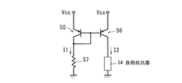
図6は、定電流源25の回路構成を示す回路図である。定電流源25は、第1トランジスタ55と、第2トランジスタ56と、抵抗器57とを含んで構成される。第1トランジスタ55と第2トランジスタ56とは、pnp型バイポーラトランジスタから成り、互いにほぼ等しい電気的特性を有する。図6では、定電流源25から見た、発光素子Tと電流迂回素子Uとから成る電気回路を、負荷抵抗器54として示している。
FIG. 6 is a circuit diagram showing a circuit configuration of the constant
第1トランジスタ55のベースと第2トランジスタ56のベースとは、相互に接続される。第1トランジスタ55のエミッタと第2トランジスタ56のエミッタとには、同電位の電圧Vccが印加される。第1トランジスタのコレクタは、抵抗器57に接続される。この抵抗器57は、グランドに接続される。第1トランジスタのベースとコレクタとは、相互に接続される。第2トランジスタ56のコレクタは、前述したように負荷抵抗器54に接続される。この負荷抵抗器54は、グランドに接続される。
The base of the
バイポーラトランジスタのエミッタ−コレクタ間が導通状態のときのベース−エミッタ間の電圧の変動は小さいので、ベースの電圧は、エミッタに印加されるエミッタ電圧Vccによって定まる。抵抗器57は、このベースに接続されるので、抵抗器57に印加される電圧は、エミッタ電圧Vccによって定まる。したがって、エミッタ電圧Vccを固定した場合、抵抗器57の抵抗値を調整することによって、抵抗器57に流れる電流I1の大きさを調整することができる。この抵抗器57に流れる電流I1は、第1トランジスタ55に流れ込む電流にほぼ等しい。
Since the fluctuation of the voltage between the base and the emitter when the emitter-collector of the bipolar transistor is in a conductive state is small, the base voltage is determined by the emitter voltage Vcc applied to the emitter. Since the
第1トランジスタ55のベース−エミッタ間の電圧と、第2トランジスタ56のベース−エミッタ間の電圧とが等しいので、第1トランジスタ55と第2トランジスタ56との電気的特性がほぼ等しい場合、第1トランジスタ55に流れ込む電流と第2トランジスタ56に流れ込む電流とは、ほぼ等しくなる。したがって、負荷抵抗器54には、抵抗器57に流れる電流I1とほぼ等しい電流I2が流れる。第1トランジスタ55に流れ込む電流は、エミッタ電位Vccを一定にした場合、抵抗器57の抵抗値によって定まるので、負荷抵抗器54のインピーダンスが変化したとしても、負荷抵抗器54に流れる電流I2の大きさは変化しない。すなわち定電流源25は、負荷抵抗器54に定電流I2を供給する。
Since the voltage between the base and the emitter of the
負荷抵抗器54がオープンモードのときには、負荷抵抗器54に電流が流れないので、第2トランジスタ56のコレクタの電圧は、エミッタ電圧Vccに近い電圧となる。エミッタ電圧Vccに近い電圧とは、具体的にはエミッタに印加される電圧Vccから、第2トランジスタのコレクタに電流が流れ込まないときのエミッタ−コレクタ間の電圧を減算した電圧である。したがって負荷抵抗器54がオープンモードのときには、負荷抵抗器54にエミッタ電圧Vccに近い電圧が印加される。
When the load resistor 54 is in the open mode, no current flows through the load resistor 54, so that the collector voltage of the
図7は、発光素子T1が、ショートモードからオープンモードに遷移した瞬間の、発光ユニットSの回路構成を示す回路図である。図8は、電流迂回素子U1がオープンモードからショートモードに遷移した後の発光ユニットSの回路構成を示す図である。 FIG. 7 is a circuit diagram showing a circuit configuration of the light emitting unit S at the moment when the light emitting element T1 transitions from the short mode to the open mode. FIG. 8 is a diagram illustrating a circuit configuration of the light emitting unit S after the current bypass element U1 transitions from the open mode to the short mode.
全ての発光素子Tが正常に発光しているとき、発光素子Tに並列に接続された電流迂回素子Uには、それぞれ順方向電圧降下V1が印加されているが、絶縁破壊電圧V2は、順方向電圧降下V1よりも高いので、電流迂回素子Uは、オープンモードを維持する。したがって電流は、電流迂回素子Uを流れずに発光素子Tを流れる。 When all the light emitting elements T are normally emitting light, a forward voltage drop V1 is applied to each of the current bypass elements U connected in parallel to the light emitting elements T, but the breakdown voltage V2 is Since it is higher than the directional voltage drop V1, the current bypass element U maintains the open mode. Therefore, the current flows through the light emitting element T without flowing through the current bypass element U.
LEDの順方向電圧降下V1の変動は、LEDに流れる電流の変動に対して小さいので、このLEDから成る発光素子Tに並列に接続される電流迂回素子Uに印加される電圧の変動も小さい。したがって、発光素子Tが正常に発光しているときに、順方向電圧降下V1が絶縁破壊電圧V2を超えることを防ぐことができ、電流迂回素子Uがショートモードに遷移することを防ぐことができる。これによって発光素子Tが正常に発光することができる状態にあるにも拘わらず、消灯することを防ぐことができ、照明装置の輝度むらの発生を抑制することができる。 Since the fluctuation of the forward voltage drop V1 of the LED is small with respect to the fluctuation of the current flowing through the LED, the fluctuation of the voltage applied to the current bypass element U connected in parallel to the light emitting element T composed of this LED is also small. Therefore, when the light emitting element T emits light normally, the forward voltage drop V1 can be prevented from exceeding the dielectric breakdown voltage V2, and the current bypass element U can be prevented from transitioning to the short mode. . Accordingly, it is possible to prevent the light emitting element T from being turned off despite being in a state where the light emitting element T can normally emit light, and to suppress occurrence of luminance unevenness of the lighting device.
全ての発光素子Tが正常に発光している状態から、1つの発光素子Tが壊れて、消灯し、ショートモードからオープンモードに遷移すると、発光素子Tは直列に接続されているので、全ての発光素子Tに電流が流れなくなり、全ての発光素子Tが消灯する。このとき、オープンモードに遷移した発光素子Tに並列に接続された電流迂回素子Uに、オープンモードに遷移した発光素子Tを除く残余の発光素子Tに印加されていた順方向電圧降下V1の合計の電圧[(n−1)×V1]が印加される。実際には、オープンモードに遷移した発光素子Tに並列に接続された発光素子Tに、定電流源25の第1および第2トランジスタ55,56のエミッタ電圧Vccに近い電圧が印加される。オープンモードに遷移した発光素子Tに並列に接続された電流迂回素子Uに印加される電圧[(n−1)×V1]が、絶縁破壊電圧V2を超えると、この電流迂回素子Uがオープンモードからショートモードに遷移する。電流迂回素子Uがオープンモードからショートモードに遷移すると、定電流源25から供給される電流は、オープンモードに遷移した電流迂回素子Uを迂回して流れるので、ショートモードに遷移した発光素子Tを除く残余の正常な発光素子Tにも電流が流れ、正常な発光素子Tは、発光状態となる。つまり、発光ユニットSのうちの、壊れた発光素子Tのみが消灯した状態となる。
When all the light emitting elements T are normally emitting light, one light emitting element T is broken and extinguished, and when the short mode is switched to the open mode, the light emitting elements T are connected in series. No current flows through the light emitting elements T, and all the light emitting elements T are turned off. At this time, the total of the forward voltage drops V1 applied to the remaining light emitting elements T excluding the light emitting elements T that have transitioned to the open mode, to the current bypass elements U connected in parallel to the light emitting elements T that have transitioned to the open mode. The voltage [(n−1) × V1] is applied. In practice, a voltage close to the emitter voltage Vcc of the first and
発光素子Tがショートモードからオープンモードに遷移し、この発光素子Tに並列に接続された電流迂回素子Uがオープンモードからショートモードに遷移すると、発光素子Tと電流迂回素子Uとを合成した負荷抵抗器54のインピーダンスが変化する。具体的には、負荷抵抗器54のインピーダンスが減少する。定電流源25は、負荷抵抗器54のインピーダンスが変化しても一定の電流を負荷抵抗器54に供給するので、各発光素子Tに流れる電流の大きさは変化せず、順方向電圧降下V1も変化しない。つまり各発光素子Tの消費電力は変動しない。発光素子Tのいずれかがオープンモードに遷移したとしても、発光素子Tの消費電力を一定に保つことができるので、各発光素子Tに過負荷を与えることを防ぎ、各発光素子Tの寿命の短縮を抑制することができる。これによって照明装置21の寿命を長くすることができる。
When the light emitting element T transitions from the short mode to the open mode, and the current bypass element U connected in parallel to the light emitting element T transitions from the open mode to the short mode, a load that combines the light emitting element T and the current bypass element U The impedance of the resistor 54 changes. Specifically, the impedance of the load resistor 54 decreases. Since the constant
本実施の形態では、n=4なので、たとえば発光素子T1がショートモードからオープンモードに遷移すると、この発光素子T1に並列に接続された電流迂回素子U1には、順方向電圧降下V1に数値3を積算した電圧(3×V1)が印加される。本実施の形態では、絶縁破壊電圧V2は、順方向電圧降下V1の2倍程度に選ばれる。したがって、発光素子T1がオープンモードに遷移すると、電流迂回素子U1に印加される電圧(3×V1)が絶縁破壊電圧V2を超え、電流迂回素子U1がオープンモードからショートモードに遷移する。これによって、発光素子T1に流れていた電流が電流迂回素子U1を迂回して流れ、発光素子T1を除く残余の発光素子T2,T3,T4に電流が流れて、発光素子T2,T3,T4は、発光状態となる。これによって壊れた発光素子T1が、正常な発光素子Tに影響を与えて、正常な発光素子Tが消灯することを防ぐことができ、照明装置21の輝度むらの発生を抑制することができる。 In this embodiment, since n = 4, for example, when the light emitting element T1 transitions from the short mode to the open mode, the current bypass element U1 connected in parallel to the light emitting element T1 has a numerical value 3 in the forward voltage drop V1. Is applied (3 × V1). In the present embodiment, the breakdown voltage V2 is selected to be about twice the forward voltage drop V1. Therefore, when the light emitting element T1 transitions to the open mode, the voltage (3 × V1) applied to the current bypass element U1 exceeds the breakdown voltage V2, and the current bypass element U1 transitions from the open mode to the short mode. As a result, the current flowing through the light emitting element T1 flows around the current bypass element U1, the current flows through the remaining light emitting elements T2, T3, T4 except the light emitting element T1, and the light emitting elements T2, T3, T4 The light emission state is activated. Thus, the broken light-emitting element T1 affects the normal light-emitting element T, and the normal light-emitting element T can be prevented from turning off, and the occurrence of uneven brightness in the lighting device 21 can be suppressed.
電流迂回素子Uは、一度ショートモードに変化すると、並列に接続された発光素子Tがオープンモードからショートモードに戻ったとしても、ショートモードを維持する。ショートモードの電流迂回素子Uにはほとんど電圧が印加されないので、ショートモードの電流迂回素子Uに並列に接続された発光素子Tがショートモードに戻ったとしても、この発光素子Tは、ほとんど電圧が印加されず、発光しない。これによって発光素子Tが点滅することを防ぐことができる。 Once the current bypass element U is changed to the short mode, the short circuit mode is maintained even if the light emitting elements T connected in parallel return from the open mode to the short mode. Since almost no voltage is applied to the short-mode current bypass element U, even if the light-emitting element T connected in parallel to the short-mode current bypass element U returns to the short mode, the light-emitting element T has almost no voltage. It is not applied and does not emit light. This can prevent the light emitting element T from blinking.
図9は、発光素子Tの光強度の方向依存性を模式的に示す図である。図9において、発光素子Tの光強度の方向依存性を、破線61を用いて示す。この破線61は、発光素子Tからの距離が長いほど、その方向の光強度が強いことを表す。本実施の形態では、発光素子Tは、ビーム拡がり角が大きいLEDによって構成される。発光ダイオードは、通常、光軸方向の光強度が最も強く、光軸方向から外れるほど、単調に光強度が弱くなるような光強度の方向依存性を有するが、本実施の形態では、発光素子Tは、光軸方向の光強度が弱く、光軸Lを含む第3方向Z方向に垂直な仮想一平面上において、光軸Lから傾斜した角度の方向の光強度が、光軸L方向の光強度よりも強くなるような光強度の方向依存性を有する。
FIG. 9 is a diagram schematically showing the direction dependency of the light intensity of the light emitting element T. FIG. In FIG. 9, the direction dependency of the light intensity of the light emitting element T is shown using a
図10は、発光ユニットSの全ての発光素子Tが発光しているときの照明装置21の光強度の方向依存性を模式的に示す断面図である。図11は、発光ユニットSの発光素子T2が消灯しているときの照明装置21の光強度の方向依存性を模式的に示す断面図である。前述したように発光ユニットSに含まれる発光素子Tは、隣接する発光素子Tと第1方向Xに第1の間隔W1をあけて設けられる。この第1の間隔W1は、照明装置21の第3方向Zの一方に想定される第3方向Zに垂直な仮想照射面上において、発光素子Tj−1(jは、2以上かつn未満の整数)からの光と、発光素子Tjからの光と、発光素子Tj+1からの光が重なるような間隔に選ばれる。本実施の形態では、第1の間隔W1は、前記仮想照射面において、発光素子Tj−1,j+1からの光のうちの光強度の強い領域が、仮想照射面と発光素子Tjの光軸Lとの交点付近において重なるように選ばれる。このように第1の間隔W1を選択することによって、たとえば発光素子Tjが消灯した場合でも、前記仮想照射面上において、発光素子Tj−1,j+1からの光によって、発光素子Tjの照射領域が完全に暗くなることを防ぐことができる。これによって、前記仮想照射面における輝度むらの発生を抑制することができる。たとえば発光素子T2が消灯した場合、前記仮想照射面において暗くなる領域が発生するが、発光素子T1,3からの光が、発光素子T2の照射領域を照射するので、輝度むらを最小限に抑えることができる。 FIG. 10 is a cross-sectional view schematically showing the direction dependency of the light intensity of the illumination device 21 when all the light emitting elements T of the light emitting unit S emit light. FIG. 11 is a cross-sectional view schematically showing the direction dependency of the light intensity of the illumination device 21 when the light emitting element T2 of the light emitting unit S is turned off. As described above, the light emitting elements T included in the light emitting unit S are provided with a first interval W1 in the first direction X with respect to the adjacent light emitting elements T. The first interval W1 is a light emitting element Tj-1 (j is 2 or more and less than n on a virtual irradiation surface perpendicular to the third direction Z assumed as one of the third directions Z of the lighting device 21. The interval is selected such that the light from the integer), the light from the light emitting element Tj, and the light from the light emitting element Tj + 1 overlap. In the present embodiment, the first interval W1 is such that the region of strong light intensity among the light from the light emitting elements Tj−1, j + 1 on the virtual irradiation surface is the optical axis L between the virtual irradiation surface and the light emitting element Tj. It is chosen to overlap in the vicinity of the intersection with. By selecting the first interval W1 in this way, even when the light emitting element Tj is turned off, for example, on the virtual irradiation surface, the irradiation region of the light emitting element Tj is caused by the light from the light emitting elements Tj−1, j + 1. It can be prevented from becoming completely dark. Thereby, it is possible to suppress the occurrence of luminance unevenness on the virtual irradiation surface. For example, when the light emitting element T2 is turned off, a darkened area is generated on the virtual irradiation surface. However, since the light from the light emitting elements T1 and 3 irradiates the irradiation area of the light emitting element T2, luminance unevenness is minimized. be able to.
また本実施の形態では、第2方向Yに隣接する発光素子Tの間隔である予め定める第2の間隔W2は、前述した予め定める第1の間隔と同じ距離に選ばれる。これによって、発光ユニットSk(kは、2以上かつn未満の整数)の発光素子Tjからの光は、発光ユニットSk−1,k+1の発光素子Tjからの光と重なり、さらに発光ユニットSkの発光素子Tj−1,j+1からの光と重なる。たとえば発光ユニットSkの発光素子Tjが消灯したとしても、この発光素子Tjからの光は、前記仮想照射面において、発光ユニットSk−1,Sk+1の発光素子Tjと、発光ユニットSkの発光素子Tj−1,j+1との4つの発光素子Tからの光によって補われる。これによって、前記仮想照射面における輝度むらの発生を抑制することができる。 In the present embodiment, the predetermined second interval W2 that is the interval between the light emitting elements T adjacent in the second direction Y is selected to be the same distance as the above-described predetermined first interval. Thereby, the light from the light emitting element Tj of the light emitting unit Sk (k is an integer of 2 or more and less than n) overlaps with the light from the light emitting element Tj of the light emitting units Sk-1, k + 1, and further the light emission of the light emitting unit Sk. It overlaps with the light from the elements Tj−1, j + 1. For example, even if the light emitting element Tj of the light emitting unit Sk is turned off, the light from the light emitting element Tj is emitted from the light emitting unit Sk-1, Sk + 1 and the light emitting element Tj− of the light emitting unit Sk on the virtual irradiation surface. Complemented by light from four light emitting elements T, 1 and j + 1. Thereby, it is possible to suppress the occurrence of luminance unevenness on the virtual irradiation surface.
図12は、前述した本実施の形態の照明装置21を備える液晶テレビジョン受信機62の基本的構成を示す正面図である。液晶テレビジョン受信機62は、キャビネット63と、スタンド64と、スピーカユニット65と、アンテナに接続される受信部と、制御部と、駆動部と、液晶表示装置22とを含んで構成される。
FIG. 12 is a front view showing a basic configuration of a liquid crystal television receiver 62 including the above-described lighting device 21 of the present embodiment. The liquid crystal television receiver 62 includes a
スタンド64は、キャビネット63を支持する。スピーカユニット65と、受信部と、制御部と、駆動部とは、キャビネット63に収容されて設けられる。スピーカユニット65は、キャビネット63の両側部にそれぞれ配置される。
The
制御部は、スピーカユニット65と、受信部と、駆動部とを制御する。制御部は、たとえば中央処理装置(Central Processing Unit:略称CPU)を含んで実現される。受信部は、アンテナによって捕捉される電波を選択して受信し、受信したテレビ信号を増幅する。テレビ信号は、音声信号と映像信号とを含む。音声信号は、スピーカユニット65に与えられる。映像信号は、駆動部に与えられる。スピーカユニット65は、与えられた音声信号を制御部の指令に基づいて増幅し、可聴表示する。駆動部は、制御部の指令に基づいて液晶表示装置22を駆動して、与えられた映像信号を可視表示させる。駆動部は、駆動用ドライバーIC(Integrated Circuit)によって実現される。
The control unit controls the
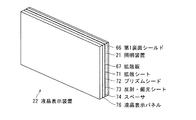
図13は、液晶表示装置22を模式的に示す斜視図である。液晶表示装置22は、第1裏面シールド66と、第1裏面シールド66の厚み方向一表面上に設けられる照明装置21と、照明装置21の厚み方向一表面上に設けられる拡散板67と、拡散板67の厚み方向一表面上に設けられる拡散シート71と、拡散シート71の厚み方向一表面上に設けられるプリズムシート72と、プリズムシート72の厚み方向一表面上に設けられる反射・偏光シート73と、反射・偏光シート73の厚み方向一表面の周縁部に設けられるスペーサ74と、スペーサ74を介して反射・偏光シート73に対向して設けられる液晶表示パネル76とを含んで構成される。 FIG. 13 is a perspective view schematically showing the liquid crystal display device 22. The liquid crystal display device 22 includes a first back shield 66, a lighting device 21 provided on one surface in the thickness direction of the first back shield 66, a diffusion plate 67 provided on one surface in the thickness direction of the lighting device 21, and a diffusion. A diffusion sheet 71 provided on one surface in the thickness direction of the plate 67, a prism sheet 72 provided on one surface in the thickness direction of the diffusion sheet 71, and a reflection / polarization sheet 73 provided on one surface in the thickness direction of the prism sheet 72. And a spacer 74 provided on the peripheral edge of one surface in the thickness direction of the reflection / polarization sheet 73, and a liquid crystal display panel 76 provided to face the reflection / polarization sheet 73 with the spacer 74 interposed therebetween.
照明装置21は、液晶表示パネル76の厚み方向の一表面に対向して設けられる。照明装置21は、白色光を発光する白色LEDから成る発光素子Tを含んで構成され、白色光を発生して液晶表示パネル76を照射するいわゆるバックライトとして機能する。照明装置21は、前述した仮想照射面が、拡散板67に一致するように配置される。このように照明装置21を配置することによって、一部の発光素子Tが消灯したとしても、拡散板67における照明装置21からの光の輝度むらの発生を最小限に抑制することができ、拡散板67に均一な光強度の光が照射される。 The lighting device 21 is provided to face one surface of the liquid crystal display panel 76 in the thickness direction. The illuminating device 21 includes a light emitting element T composed of a white LED that emits white light, and functions as a so-called backlight that emits white light and irradiates the liquid crystal display panel 76. The illuminating device 21 is arranged so that the above-described virtual irradiation surface coincides with the diffusion plate 67. By arranging the illuminating device 21 in this manner, even if some of the light emitting elements T are turned off, the unevenness of the luminance of the light from the illuminating device 21 in the diffusing plate 67 can be suppressed to the minimum, and the diffusion The plate 67 is irradiated with light having a uniform light intensity.
第1裏面シールド66は、液晶表示装置22を機械的衝撃などから保護する。拡散板67および拡散シート71は、それぞれ通過する光を散乱して拡散する半透明の板およびシートから成る。拡散板67には、輝度むらの少ない光が照射されるが、この光が拡散板67および拡散シート71を通過することによって、照明装置21の厚み方向に垂直な仮想平面上においてさらに均一な輝度むらの少ない光となる。拡散シート71を通過した光は、プリズムシート72を通過して、反射・偏光シート73により目的とする偏光成分のみが透過し、液晶表示パネル76に集光される。 The first back shield 66 protects the liquid crystal display device 22 from mechanical shocks and the like. The diffusion plate 67 and the diffusion sheet 71 are each composed of a translucent plate and a sheet that scatter and diffuse light passing therethrough. The diffuser plate 67 is irradiated with light with less luminance unevenness, and this light passes through the diffuser plate 67 and the diffuser sheet 71, thereby further uniforming the luminance on a virtual plane perpendicular to the thickness direction of the illumination device 21. The light is less uneven. The light that has passed through the diffusion sheet 71 passes through the prism sheet 72, and only the desired polarization component is transmitted by the reflection / polarization sheet 73 and is condensed on the liquid crystal display panel 76.
液晶表示パネル76は、アクティブマトリクス駆動法によって駆動され、液晶層と、1対の配向膜と、1対の透明電極と、1対のガラス基板と、カラーフィルタと、1対の偏光フィルタとを含んで構成される。液晶層は、スペーサを挟んで対向して配置される1対の配向膜の間に充填される。透明電極は、1対の配向膜を挟んで対向して配置される。カラーフィルタは、1対の配向膜のうちの照明装置21から離間する一方の厚み方向一表面上に設けられる。1対のガラス基板は、カラーフィルタと他方の配向膜とを挟んで対向して配置される。1対の偏光フィルタは、1対のガラス基板を挟んで対向して設けられる。 The liquid crystal display panel 76 is driven by an active matrix driving method, and includes a liquid crystal layer, a pair of alignment films, a pair of transparent electrodes, a pair of glass substrates, a color filter, and a pair of polarizing filters. Consists of including. The liquid crystal layer is filled between a pair of alignment films arranged to face each other with a spacer interposed therebetween. The transparent electrodes are arranged to face each other with a pair of alignment films interposed therebetween. The color filter is provided on one surface in the thickness direction that is separated from the illumination device 21 in the pair of alignment films. The pair of glass substrates are disposed to face each other with the color filter and the other alignment film interposed therebetween. The pair of polarizing filters are provided to face each other with a pair of glass substrates interposed therebetween.
駆動部は、制御部の指令に基づいて透明電極に与える電圧を制御することによって、照明装置21から照射される光のうちの一部を選択的に液晶表示パネル76を透過させ、液晶表示パネル76に映像信号を可視表示させる。 The drive unit controls the voltage applied to the transparent electrode based on a command from the control unit, thereby selectively transmitting a part of the light emitted from the illumination device 21 through the liquid crystal display panel 76. The video signal is displayed in the visual display 76.
図14は、本発明の他の実施の形態の照明装置21の発光ユニットSを模式的に示す断面図である。図15は、発光素子Tと電流迂回素子Uとが形成された半導体ウエハ81の平面図である。本発明の他の実施の形態では、前述の実施の形態の発光素子Tと電流迂回素子Uとが、電気絶縁性を有する電気絶縁部83を挟んで1つのモジュール82として一体に形成される。
FIG. 14 is a cross-sectional view schematically showing a light emitting unit S of a lighting device 21 according to another embodiment of the present invention. FIG. 15 is a plan view of the
モジュール82は、略直方体形状を有し、一方電極層84と、他方電極層85と、電流迂回素子Uと、発光素子Tと、電気絶縁部83とを含んで構成される。一方電極層84は、導電性を有し、モジュール82の厚み方向他表面部を構成する。他方電極層85は、導電性を有し、モジュール82の厚み方向一表面部を構成する。
The
電流迂回素子Uは、モジュール82の厚み方向一方から見て、四角形の四隅のうちの1つの隅部に、モジュール82の厚み方向の一端から他端にわたって形成される。電流迂回素子Uの一方導電層42は、一方電極層84の一部を構成し、他方導電層43は、他方電極層85の一部を構成する。
The current bypass element U is formed at one corner of the four corners of the square from one end in the thickness direction of the
電気絶縁部83は、電流迂回素子Uの一方ポリシリコン層44と、他方ポリシリコン層45と、電気絶縁層46との厚み方向に垂直な方向の表面を覆うように、一方電極層84と他方電極層85との間にわたって形成される。
The electric insulating
発光素子Tは、モジュール82のうちの電流迂回素子Uおよび電気絶縁部83を除く残余の部分を構成する。発光素子Tのn型半導体層34およびp型半導体層36は、電気絶縁部83によって、一方ポリシリコン層44、電気絶縁層46および他方ポリシリコン層45と電気的に絶縁される。カソードKは、一方電極層84の一部を構成する。つまり一方電極層84は、発光素子TのカソードKと電流迂回素子Uの一方導電層42との共通の電極として形成され、カソードKと一方電極層84とが電気的に接続される。アノードAは、他方電極層85の一部を構成する。つまり他方電極層85は、発光素子TのアノードAと電流迂回素子Uの他方導電層43との共通の電極として形成され、アノードAと他方導電層43とが電気的に接続される。
The light emitting element T constitutes the remaining part of the
半導体ウエハ81には、複数のモジュール82が半導体プロセスを用いて形成される。このように半導体ウエハ81に形成された複数のモジュール82を、それぞれ1つずつのモジュール82に切り離すことによって、モジュール82が作成される。
A plurality of
発光素子Tと電流迂回素子Uとは一体に形成されるので、発光素子Tと電流迂回素子Uとを一度の工程でプリント配線基板24に実装することができる。また発光素子TのアノードKと電流迂回素子Uの他方導電層43とをワイヤ41で接続する工程を省略することができる。これによって別々にプリント配線基板24に実装する場合に比べて工程数を少なくすることができ、照明装置21を作成するコストを低減することができる。
Since the light emitting element T and the current bypass element U are integrally formed, the light emitting element T and the current bypass element U can be mounted on the printed
また発光素子Tと電流迂回素子Uとを一体に形成することによって、モジュール82の小形化を実現することができ、照明装置21の小形化を実現することができる。
Further, by integrally forming the light emitting element T and the current bypass element U, the
本発明のさらに他の実施の形態では、前述の電流迂回素子Uは、アンチヒューズに限らず、絶縁破壊電圧V2が印加されたときにオープンモードからショートモードに遷移する素子によって構成される。電流迂回素子Uは、たとえばタンタル電解コンデンサによって実現される。この場合、タンタル電解コンデンサの陽極は、発光素子TのアノードAに電気的に接続され、タンタル電解コンデンサの陰極は、発光素子TのカソードKに電気的に接続される。タンタル電解コンデンサは、絶縁破壊電圧V2が印加されたときにオープンモードからショートモードに遷移するので、前述したように発光素子Tがオープンモードに遷移したときに、この発光素子Tに並列に接続されたタンタル電解コンデンサがショートモードに遷移する。タンタル電解コンデンサによって構成される電流迂回素子Uは、コンデンサとしても機能するので、並列に接続される発光素子Tの順方向電圧降下V1の変動を緩和する。これによって、発光素子Tから発生する電気的ノイズを除去することができる。 In still another embodiment of the present invention, the above-described current bypass element U is not limited to an antifuse, and is configured by an element that transitions from an open mode to a short mode when a dielectric breakdown voltage V2 is applied. The current bypass element U is realized by a tantalum electrolytic capacitor, for example. In this case, the anode of the tantalum electrolytic capacitor is electrically connected to the anode A of the light emitting element T, and the cathode of the tantalum electrolytic capacitor is electrically connected to the cathode K of the light emitting element T. Since the tantalum electrolytic capacitor transitions from the open mode to the short mode when the dielectric breakdown voltage V2 is applied, as described above, when the light emitting element T transitions to the open mode, the tantalum electrolytic capacitor is connected in parallel to the light emitting element T. The tantalum electrolytic capacitor transitions to the short mode. Since the current bypass element U constituted by the tantalum electrolytic capacitor also functions as a capacitor, the fluctuation of the forward voltage drop V1 of the light emitting elements T connected in parallel is reduced. Thereby, electrical noise generated from the light emitting element T can be removed.
本発明のさらに他の実施の形態では、発光素子Tは、マトリックス状に限らずに、どのように配列してもよい。たとえば発光素子Tは、千鳥格子状に配列されてもよい。 In still another embodiment of the present invention, the light emitting elements T are not limited to a matrix shape and may be arranged in any manner. For example, the light emitting elements T may be arranged in a staggered pattern.
本発明のさらに他の実施の形態では、発光ユニットSの数mは、数値3に限らず、発光素子Tの数nは、数値nに限らずに、どのような数値としても良い。たとえば発光ユニットSの数mが40で、発光素子Tの数nが25の、1000個の発光素子Tから成る照明装置21を構成してもよい。この場合でも、壊れた発光素子Tのみが消灯するので、輝度むらの少ない照明装置21が実現される。 In still another embodiment of the present invention, the number m of the light emitting units S is not limited to the numerical value 3, and the number n of the light emitting elements T is not limited to the numerical value n and may be any numerical value. For example, the illuminating device 21 composed of 1000 light emitting elements T in which the number m of the light emitting units S is 40 and the number n of the light emitting elements T is 25 may be configured. Even in this case, since only the broken light emitting element T is turned off, the illumination device 21 with less luminance unevenness is realized.
本実施の形態では、照明装置21は、液晶表示装置22のバックライトに用いられるとしたけれども、バックライトに限らず、透過型表示素子を備える透過型表示装置または半透過型表示装置などにも好適に用いられる。 In the present embodiment, the illumination device 21 is used as a backlight of the liquid crystal display device 22, but is not limited to the backlight, and is also used for a transmissive display device or a transflective display device including a transmissive display element. Preferably used.
また本実施の形態では、発光素子Tは、LEDから成るとしたけれども、LEDに限らず、直流電圧で駆動する、蛍光灯、ハロゲンランプおよび電球などの照明装置によって構成されてもよい。 In the present embodiment, the light emitting element T is composed of LEDs. However, the light emitting elements T are not limited to LEDs, and may be composed of lighting devices such as fluorescent lamps, halogen lamps, and light bulbs that are driven by a DC voltage.
21 照明装置
22 液晶表示装置
25 定電流源
31 保護部
32 ランド
41 ワイヤ
62 液晶テレビジョン受信機
76 液晶表示パネル
S 発光ユニット
T 発光素子
U 電流迂回素子
DESCRIPTION OF SYMBOLS 21 Illuminating device 22 Liquid
Claims (4)
前記直列に接続される複数の発光素子に直列に接続され、各発光素子に電力を供給する電源部と、
各発光素子に個別に並列に接続され、各発光素子が発光状態のときに印加される電圧よりも高い予め定める電圧が印加されたときに、電流が流れない非導通状態から電流が流れる導通状態に変化する複数の電流迂回素子とを含むことを特徴とする照明装置。 A plurality of light emitting elements connected in series with each other and emitting light by applying a voltage;
A power supply unit connected in series to the plurality of light emitting elements connected in series and supplying power to each light emitting element;
A conductive state in which a current flows from a non-conductive state where no current flows when a predetermined voltage higher than the voltage applied when each light emitting element is in a light emitting state is applied in parallel to each light emitting element. A lighting device comprising: a plurality of current bypass elements that change to
前記電流迂回素子は、前記予め定める電圧が印加されたときに、非導通状態から導通状態に遷移することを特徴とする請求項1記載の照明装置。 The power supply unit includes a constant current source that supplies a constant current to the plurality of light emitting elements,
The lighting device according to claim 1, wherein the current bypass element transitions from a non-conductive state to a conductive state when the predetermined voltage is applied.
液晶表示パネルの厚み方向の一表面に対向して設けられる請求項1〜3のいずれか1つに記載の照明装置とを含むことを特徴とする液晶表示装置。 A liquid crystal display panel;
A liquid crystal display device comprising: the lighting device according to claim 1 provided to face one surface in a thickness direction of the liquid crystal display panel.
Priority Applications (1)
| Application Number | Priority Date | Filing Date | Title |
|---|---|---|---|
| JP2006014406A JP2007200577A (en) | 2006-01-23 | 2006-01-23 | Lighting device and liquid crystal display device |
Applications Claiming Priority (1)
| Application Number | Priority Date | Filing Date | Title |
|---|---|---|---|
| JP2006014406A JP2007200577A (en) | 2006-01-23 | 2006-01-23 | Lighting device and liquid crystal display device |
Publications (1)
| Publication Number | Publication Date |
|---|---|
| JP2007200577A true JP2007200577A (en) | 2007-08-09 |
Family
ID=38454993
Family Applications (1)
| Application Number | Title | Priority Date | Filing Date |
|---|---|---|---|
| JP2006014406A Pending JP2007200577A (en) | 2006-01-23 | 2006-01-23 | Lighting device and liquid crystal display device |
Country Status (1)
| Country | Link |
|---|---|
| JP (1) | JP2007200577A (en) |
Cited By (12)
| Publication number | Priority date | Publication date | Assignee | Title |
|---|---|---|---|---|
| JP2008053663A (en) * | 2006-08-28 | 2008-03-06 | Matsushita Electric Works Ltd | Led unit |
| WO2010071131A1 (en) * | 2008-12-17 | 2010-06-24 | パナソニック電工株式会社 | Light emission apparatus |
| WO2010100995A1 (en) * | 2009-03-02 | 2010-09-10 | 株式会社 村田製作所 | Antifuse device |
| WO2010063023A3 (en) * | 2008-11-30 | 2010-09-16 | Cree, Inc. | Electronic device including circuitry comprising open failure-susceptible components, and open failure-actuated anti-fuse pathway |
| WO2011004874A1 (en) * | 2009-07-09 | 2011-01-13 | 株式会社村田製作所 | Anti-fuse element |
| WO2011142248A1 (en) * | 2010-05-14 | 2011-11-17 | Necライティング株式会社 | Organic el illumination device |
| WO2013023609A1 (en) * | 2011-08-16 | 2013-02-21 | Huizhou Light Engine Limited | Light engine with led switching array |
| US8436371B2 (en) | 2007-05-24 | 2013-05-07 | Cree, Inc. | Microscale optoelectronic device packages |
| JP2013236826A (en) * | 2012-05-16 | 2013-11-28 | Daiichi Shokai Co Ltd | Game machine |
| WO2015060278A1 (en) * | 2013-10-24 | 2015-04-30 | 株式会社村田製作所 | Composite protection circuit, composite protection element, and led element for lighting |
| JP2017157612A (en) * | 2016-02-29 | 2017-09-07 | 日亜化学工業株式会社 | Laser element |
| US9781803B2 (en) | 2008-11-30 | 2017-10-03 | Cree, Inc. | LED thermal management system and method |
Citations (2)
| Publication number | Priority date | Publication date | Assignee | Title |
|---|---|---|---|---|
| JP2002025784A (en) * | 2000-04-28 | 2002-01-25 | Takashi Ishizawa | Led-lighting circuit |
| JP2005310998A (en) * | 2004-04-20 | 2005-11-04 | Sony Corp | Fixed current driving device, back light optical source apparatus and color liquid crystal display device |
-
2006
- 2006-01-23 JP JP2006014406A patent/JP2007200577A/en active Pending
Patent Citations (2)
| Publication number | Priority date | Publication date | Assignee | Title |
|---|---|---|---|---|
| JP2002025784A (en) * | 2000-04-28 | 2002-01-25 | Takashi Ishizawa | Led-lighting circuit |
| JP2005310998A (en) * | 2004-04-20 | 2005-11-04 | Sony Corp | Fixed current driving device, back light optical source apparatus and color liquid crystal display device |
Cited By (25)
| Publication number | Priority date | Publication date | Assignee | Title |
|---|---|---|---|---|
| JP2008053663A (en) * | 2006-08-28 | 2008-03-06 | Matsushita Electric Works Ltd | Led unit |
| US8436371B2 (en) | 2007-05-24 | 2013-05-07 | Cree, Inc. | Microscale optoelectronic device packages |
| US9781803B2 (en) | 2008-11-30 | 2017-10-03 | Cree, Inc. | LED thermal management system and method |
| US8643283B2 (en) | 2008-11-30 | 2014-02-04 | Cree, Inc. | Electronic device including circuitry comprising open failure-susceptible components, and open failure-actuated anti-fuse pathway |
| WO2010063023A3 (en) * | 2008-11-30 | 2010-09-16 | Cree, Inc. | Electronic device including circuitry comprising open failure-susceptible components, and open failure-actuated anti-fuse pathway |
| WO2010071131A1 (en) * | 2008-12-17 | 2010-06-24 | パナソニック電工株式会社 | Light emission apparatus |
| JP2010147189A (en) * | 2008-12-17 | 2010-07-01 | Panasonic Electric Works Co Ltd | Light-emitting device |
| WO2010100995A1 (en) * | 2009-03-02 | 2010-09-10 | 株式会社 村田製作所 | Antifuse device |
| CN102341904A (en) * | 2009-03-02 | 2012-02-01 | 株式会社村田制作所 | Antifuse device |
| JPWO2010100995A1 (en) * | 2009-03-02 | 2012-09-06 | 株式会社村田製作所 | Antifuse element |
| EP2405479A1 (en) * | 2009-03-02 | 2012-01-11 | Murata Manufacturing Co., Ltd. | Antifuse device |
| EP2405479A4 (en) * | 2009-03-02 | 2013-12-04 | Murata Manufacturing Co | Antifuse device |
| US8896092B2 (en) | 2009-07-09 | 2014-11-25 | Murata Manufacturing Co., Ltd. | Anti-fuse element |
| WO2011004874A1 (en) * | 2009-07-09 | 2011-01-13 | 株式会社村田製作所 | Anti-fuse element |
| JP5387677B2 (en) * | 2009-07-09 | 2014-01-15 | 株式会社村田製作所 | Antifuse element |
| WO2011142248A1 (en) * | 2010-05-14 | 2011-11-17 | Necライティング株式会社 | Organic el illumination device |
| JPWO2011142248A1 (en) * | 2010-05-14 | 2013-07-22 | Necライティング株式会社 | Organic EL lighting device |
| US8754408B2 (en) | 2010-05-14 | 2014-06-17 | Nec Lighting, Ltd. | Organic EL illumination device |
| CN102954366A (en) * | 2011-08-16 | 2013-03-06 | 惠州元晖光电股份有限公司 | Light engine with led switching array |
| US9357604B2 (en) | 2011-08-16 | 2016-05-31 | Huizhou Light Engine Ltd. | Light engine with LED switching array |
| WO2013023609A1 (en) * | 2011-08-16 | 2013-02-21 | Huizhou Light Engine Limited | Light engine with led switching array |
| JP2013236826A (en) * | 2012-05-16 | 2013-11-28 | Daiichi Shokai Co Ltd | Game machine |
| WO2015060278A1 (en) * | 2013-10-24 | 2015-04-30 | 株式会社村田製作所 | Composite protection circuit, composite protection element, and led element for lighting |
| US10043786B2 (en) | 2013-10-24 | 2018-08-07 | Murata Manufacturing Co., Ltd. | Composite protection circuit, composite protection element, and LED device for illumination |
| JP2017157612A (en) * | 2016-02-29 | 2017-09-07 | 日亜化学工業株式会社 | Laser element |
Similar Documents
| Publication | Publication Date | Title |
|---|---|---|
| JP2007200577A (en) | Lighting device and liquid crystal display device | |
| JP4963471B2 (en) | Illumination device and liquid crystal display device | |
| US8503500B2 (en) | Alternating current light emitting device | |
| US20170069680A1 (en) | Light-emitting device | |
| JP4588571B2 (en) | Illumination device and display device including the same | |
| US9153732B2 (en) | Active LED module | |
| US7884553B2 (en) | Light-emitting diode illumination circuit, illumination device, and liquid crystal display apparatus | |
| JP4172501B2 (en) | Light emitting diode lighting circuit, lighting device, and liquid crystal display device | |
| JP5840225B2 (en) | Power supply device | |
| US20130001606A1 (en) | Sub-mount, light emitting device including sub-mount and methods of manufacturing such sub-mount and/or light emitting device | |
| EP3934383A1 (en) | Light emission element substrate, display device, and method of repairing display device | |
| US10490121B2 (en) | Display device | |
| KR20110128741A (en) | Semiconductor light-emitting element, light-emitting device, luminaire, display unit, traffic signal lamp unit, and traffic information display unit | |
| WO2007069148A2 (en) | Semiconductor light source and method of producing light of a desired color point | |
| US20210194208A1 (en) | Light source device | |
| KR20060084315A (en) | Led array circuit | |
| US20090207633A1 (en) | Backlight Unit and Display Including the Same | |
| US7417260B2 (en) | Multiple-chromatic light emitting device | |
| JP2011060680A (en) | Lighting system and electronic equipment | |
| WO2018230454A1 (en) | Lighting device and display device | |
| US20210066563A1 (en) | Semiconductor device and light emitting element package including same | |
| US8569962B2 (en) | LED driver circuit and LED driver system | |
| KR20120111757A (en) | Light emitting device package | |
| KR102431684B1 (en) | Lighting emitting diode package and liquid crystal display device including the same | |
| US20200357973A1 (en) | Display apparatus |
Legal Events
| Date | Code | Title | Description |
|---|---|---|---|
| A621 | Written request for application examination |
Free format text: JAPANESE INTERMEDIATE CODE: A621 Effective date: 20080220 |
|
| A977 | Report on retrieval |
Free format text: JAPANESE INTERMEDIATE CODE: A971007 Effective date: 20101015 |
|
| A131 | Notification of reasons for refusal |
Free format text: JAPANESE INTERMEDIATE CODE: A131 Effective date: 20101019 |
|
| A02 | Decision of refusal |
Free format text: JAPANESE INTERMEDIATE CODE: A02 Effective date: 20110301 |