JP2007200542A - System comprising memory module mounted with semiconductor memory device - Google Patents
System comprising memory module mounted with semiconductor memory device Download PDFInfo
- Publication number
- JP2007200542A JP2007200542A JP2007047258A JP2007047258A JP2007200542A JP 2007200542 A JP2007200542 A JP 2007200542A JP 2007047258 A JP2007047258 A JP 2007047258A JP 2007047258 A JP2007047258 A JP 2007047258A JP 2007200542 A JP2007200542 A JP 2007200542A
- Authority
- JP
- Japan
- Prior art keywords
- clock signal
- signal
- address
- command
- memory module
- Prior art date
- Legal status (The legal status is an assumption and is not a legal conclusion. Google has not performed a legal analysis and makes no representation as to the accuracy of the status listed.)
- Granted
Links
- 239000004065 semiconductor Substances 0.000 title claims abstract description 28
- 230000004044 response Effects 0.000 claims abstract description 45
- 230000001360 synchronised effect Effects 0.000 claims description 3
- 230000006870 function Effects 0.000 abstract 1
- 102100040862 Dual specificity protein kinase CLK1 Human genes 0.000 description 52
- 102100040844 Dual specificity protein kinase CLK2 Human genes 0.000 description 30
- 101000749291 Homo sapiens Dual specificity protein kinase CLK2 Proteins 0.000 description 30
- 101000749294 Homo sapiens Dual specificity protein kinase CLK1 Proteins 0.000 description 27
- 238000010586 diagram Methods 0.000 description 8
- 230000000630 rising effect Effects 0.000 description 6
- 238000000034 method Methods 0.000 description 3
- 230000005540 biological transmission Effects 0.000 description 1
- 238000012986 modification Methods 0.000 description 1
- 230000004048 modification Effects 0.000 description 1
Images


Classifications
-
- G—PHYSICS
- G11—INFORMATION STORAGE
- G11C—STATIC STORES
- G11C7/00—Arrangements for writing information into, or reading information out from, a digital store
- G11C7/10—Input/output [I/O] data interface arrangements, e.g. I/O data control circuits, I/O data buffers
- G11C7/1078—Data input circuits, e.g. write amplifiers, data input buffers, data input registers, data input level conversion circuits
- G11C7/1084—Data input buffers, e.g. comprising level conversion circuits, circuits for adapting load
-
- G—PHYSICS
- G11—INFORMATION STORAGE
- G11C—STATIC STORES
- G11C11/00—Digital stores characterised by the use of particular electric or magnetic storage elements; Storage elements therefor
- G11C11/21—Digital stores characterised by the use of particular electric or magnetic storage elements; Storage elements therefor using electric elements
- G11C11/34—Digital stores characterised by the use of particular electric or magnetic storage elements; Storage elements therefor using electric elements using semiconductor devices
- G11C11/40—Digital stores characterised by the use of particular electric or magnetic storage elements; Storage elements therefor using electric elements using semiconductor devices using transistors
- G11C11/401—Digital stores characterised by the use of particular electric or magnetic storage elements; Storage elements therefor using electric elements using semiconductor devices using transistors forming cells needing refreshing or charge regeneration, i.e. dynamic cells
- G11C11/4063—Auxiliary circuits, e.g. for addressing, decoding, driving, writing, sensing or timing
- G11C11/407—Auxiliary circuits, e.g. for addressing, decoding, driving, writing, sensing or timing for memory cells of the field-effect type
- G11C11/4076—Timing circuits
-
- G—PHYSICS
- G11—INFORMATION STORAGE
- G11C—STATIC STORES
- G11C11/00—Digital stores characterised by the use of particular electric or magnetic storage elements; Storage elements therefor
- G11C11/21—Digital stores characterised by the use of particular electric or magnetic storage elements; Storage elements therefor using electric elements
- G11C11/34—Digital stores characterised by the use of particular electric or magnetic storage elements; Storage elements therefor using electric elements using semiconductor devices
- G11C11/40—Digital stores characterised by the use of particular electric or magnetic storage elements; Storage elements therefor using electric elements using semiconductor devices using transistors
- G11C11/401—Digital stores characterised by the use of particular electric or magnetic storage elements; Storage elements therefor using electric elements using semiconductor devices using transistors forming cells needing refreshing or charge regeneration, i.e. dynamic cells
- G11C11/4063—Auxiliary circuits, e.g. for addressing, decoding, driving, writing, sensing or timing
- G11C11/407—Auxiliary circuits, e.g. for addressing, decoding, driving, writing, sensing or timing for memory cells of the field-effect type
- G11C11/408—Address circuits
- G11C11/4082—Address Buffers; level conversion circuits
-
- G—PHYSICS
- G11—INFORMATION STORAGE
- G11C—STATIC STORES
- G11C11/00—Digital stores characterised by the use of particular electric or magnetic storage elements; Storage elements therefor
- G11C11/21—Digital stores characterised by the use of particular electric or magnetic storage elements; Storage elements therefor using electric elements
- G11C11/34—Digital stores characterised by the use of particular electric or magnetic storage elements; Storage elements therefor using electric elements using semiconductor devices
- G11C11/40—Digital stores characterised by the use of particular electric or magnetic storage elements; Storage elements therefor using electric elements using semiconductor devices using transistors
- G11C11/401—Digital stores characterised by the use of particular electric or magnetic storage elements; Storage elements therefor using electric elements using semiconductor devices using transistors forming cells needing refreshing or charge regeneration, i.e. dynamic cells
- G11C11/4063—Auxiliary circuits, e.g. for addressing, decoding, driving, writing, sensing or timing
- G11C11/407—Auxiliary circuits, e.g. for addressing, decoding, driving, writing, sensing or timing for memory cells of the field-effect type
- G11C11/409—Read-write [R-W] circuits
- G11C11/4093—Input/output [I/O] data interface arrangements, e.g. data buffers
-
- G—PHYSICS
- G11—INFORMATION STORAGE
- G11C—STATIC STORES
- G11C7/00—Arrangements for writing information into, or reading information out from, a digital store
- G11C7/10—Input/output [I/O] data interface arrangements, e.g. I/O data control circuits, I/O data buffers
- G11C7/1072—Input/output [I/O] data interface arrangements, e.g. I/O data control circuits, I/O data buffers for memories with random access ports synchronised on clock signal pulse trains, e.g. synchronous memories, self timed memories
-
- G—PHYSICS
- G11—INFORMATION STORAGE
- G11C—STATIC STORES
- G11C7/00—Arrangements for writing information into, or reading information out from, a digital store
- G11C7/10—Input/output [I/O] data interface arrangements, e.g. I/O data control circuits, I/O data buffers
- G11C7/1078—Data input circuits, e.g. write amplifiers, data input buffers, data input registers, data input level conversion circuits
- G11C7/109—Control signal input circuits
-
- G—PHYSICS
- G11—INFORMATION STORAGE
- G11C—STATIC STORES
- G11C7/00—Arrangements for writing information into, or reading information out from, a digital store
- G11C7/22—Read-write [R-W] timing or clocking circuits; Read-write [R-W] control signal generators or management
-
- G—PHYSICS
- G11—INFORMATION STORAGE
- G11C—STATIC STORES
- G11C7/00—Arrangements for writing information into, or reading information out from, a digital store
- G11C7/22—Read-write [R-W] timing or clocking circuits; Read-write [R-W] control signal generators or management
- G11C7/222—Clock generating, synchronizing or distributing circuits within memory device
-
- G—PHYSICS
- G11—INFORMATION STORAGE
- G11C—STATIC STORES
- G11C8/00—Arrangements for selecting an address in a digital store
- G11C8/18—Address timing or clocking circuits; Address control signal generation or management, e.g. for row address strobe [RAS] or column address strobe [CAS] signals
Landscapes
- Engineering & Computer Science (AREA)
- Microelectronics & Electronic Packaging (AREA)
- Computer Hardware Design (AREA)
- Dram (AREA)
Abstract
Description
本発明は半導体メモリ装置及びこれを含むメモリモジュールを有するシステムに係り、特にシステムのクロック周波数が高まっても低い周波数の内部クロック信号を作ってアドレス信号及びコマンド信号の動作周波数として使用し、相異なる周波数を有するクロック信号を受信する半導体メモリ装置及びこれを含むメモリモジュールを有するシステムに関する。 The present invention relates to a semiconductor memory device and a system having a memory module including the semiconductor memory device. Particularly, even if the clock frequency of the system is increased, an internal clock signal having a low frequency is generated and used as an operating frequency of an address signal and a command signal. The present invention relates to a semiconductor memory device that receives a clock signal having a frequency and a system having a memory module including the semiconductor memory device.
最近のコンピュータシステムは、高性能マイクロコントローラ(以下"CPU"と称する)の開発によって大容量のデータを高速で処理することが要求される。このような要求は、CPUの命令構造及び機能構造によってプロセッサのワード長さをより大きくし、クロック周波数を増加させ、またデータバス幅を大きくするなどCPUの特性によるものである。特に、クロック周波数の増加はCPUとデータとを相互交換するメモリの容量を大きくし、データ伝送速度を速くするように誘導する。したがって、メモリは高周波のシステムクロック信号に合せて動作する。 Recent computer systems are required to process a large amount of data at high speed by developing a high performance microcontroller (hereinafter referred to as "CPU"). Such a request is due to the characteristics of the CPU, such as increasing the word length of the processor, increasing the clock frequency, and increasing the data bus width depending on the instruction structure and functional structure of the CPU. In particular, an increase in the clock frequency leads to an increase in the capacity of the memory for exchanging CPU and data and an increase in data transmission speed. Therefore, the memory operates in accordance with the high frequency system clock signal.
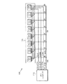
図1は、メモリコントローラ110とメモリモジュール120とを具備する一般的なシステムボード100を示す図面である。メモリコントローラ110はクロックバスライン、アドレスバスライン、コマンドバスライン、及びデータバスラインを通じてクロック信号CLK、アドレス信号ADDR、コマンド信号CMD及びデータDATAをメモリモジュール120に伝送する。メモリモジュール120は、一例として8個のメモリチップ101、102、…、108を内蔵し、各メモリチップ101、102、…、108はクロックバスライン、アドレスバスライン、コマンドバスライン及びデータバスラインと連結される。
FIG. 1 is a diagram illustrating a
システムの高機能化、高性能化によって、クロックバスラインにのせられるクロック信号CLKの周波数が高まる。高周波数のクロック信号CLKはメモリチップ101、102、…、108に提供されてメモリチップ101、102、…、108の動作を制御する。メモリチップ101、102、…、108が、例えばSDRAMの場合に、クロック信号CLKのエッジに合せてコマンド信号CMD、アドレス信号ADDR、そしてデータDATAを受信または入出力する。
With the higher functionality and higher performance of the system, the frequency of the clock signal CLK placed on the clock bus line increases. The high frequency clock signal CLK is provided to the
ところが、図1で分かるように、メモリチップ101、102、…、108から入出力されるデータDATAは各メモリチップ101、102、…、108に連結された独立的なデータラインを通じてデータバスラインと連結される。それで、それぞれのデータラインの負荷はこれと連結される一つのメモリチップになる。これに反してアドレスバス及びコマンドバスはメモリチップ101、102、…、108に直列に共有されて連結されるために、アドレス信号ADDR及びコマンド信号CMDは8つのメモリチップ101、102、…、108に該当する負荷を有する。
However, as can be seen in FIG. 1, data DATA input / output from the
それで、クロック信号CLKの高周波化によってデータラインにのせられるデータDATAは該当負荷が小さいためにクロック信号CLKによって高周波動作が可能であるが、アドレス信号ADDR及びコマンド信号CMDは該当負荷が大きいためにクロック信号CLKによる高周波動作に限界がある。 Therefore, the data DATA placed on the data line due to the high frequency of the clock signal CLK can be operated at a high frequency by the clock signal CLK because the corresponding load is small, but the address signal ADDR and the command signal CMD are clocked because the corresponding load is large. There is a limit to the high-frequency operation by the signal CLK.
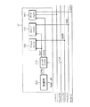
図2は、システムボードに装着された従来のメモリモジュール120を示す図面である。システムボードにはマイクロプロセッサ(図示せず)またはメモリコントローラ(図示せず)と連結される多数のバスラインが配置されるが、代表的にクロックバスラインCLK、アドレスバスラインADDR及びコマンドバスラインCMDが配置される。メモリモジュール120は多数のメモリチップ101、102、…、106、位相同期回路(Phase Locked Loop: 以下"PLL"と称する)107及びレジスタ108を含む。
FIG. 2 is a diagram illustrating a
PLL107は、クロックバスラインにのせられるクロック信号CLKを受信して多数の内部クロック信号ICLK0、ICLK1、ICLK2…、ICLK6を発生させる。内部クロック信号ICLK0、ICLK1、ICLK2、…、ICLK6はスキューなしに同じスルーレートとデューティを有する理想的な信号である。そして内部クロック信号ICLK0、ICLK1、ICLK2、…、ICLK6はクロック信号CLKと位相が同期するために、クロック信号CLKの周波数を有する。内部クロック信号ICLK0はレジスタ108に提供され、内部クロック信号ICLK1、ICLK2、…、ICLK6はメモリチップ101、102、…、106に提供される。図2で、一つのクロック信号が一つのメモリチップに連結されているが、実際の応用で一つのクロック信号が対応するメモリチップの数は可変的でありうる。レジスタ108は内部クロック信号ICLK0に応答してアドレス信号ADDR及びコマンド信号CMDを受信した後、それらを各メモリチップ101、102、…、106に伝送する。
The
ところが、メモリモジュール120は、一つのクロック信号CLKだけを受信してこれを多数の内部クロック信号ICLK0、ICLK1、ICLK2、…ICLK6に作るために、高性能システムの場合、クロック信号CLKの周波数が高まれば、これにより内部クロック信号ICLK0、ICLK1、ICLK2、…、ICLK6の周波数も高まる。内部クロック信号ICLK1、ICLK2、…、ICLK6を受信してこれにより動作するメモリチップ101、102、…、106はそれ自体高周波動作に適したデバイスで構成できるためにその動作に問題はないが、レジスタ108の場合は、内部クロック信号ICLK0の周波数、すなわち、高周波数によってアドレス信号ADDR及びコマンド信号CMDを受信し、これを高周波数に合せてメモリチップに伝達できるかどうかは疑わしい。
However, since the
したがって、クロック信号CLKの周波数が高まってもアドレス信号ADDR及びコマンド信号CMDの動作周波数を任意に低めて使用でき、レジスタ108の動作に適したクロック信号を受信できるメモリ装置及びメモリモジュールが要求される。
Therefore, there is a need for a memory device and a memory module that can be used by arbitrarily reducing the operating frequency of the address signal ADDR and the command signal CMD even when the frequency of the clock signal CLK is increased and can receive a clock signal suitable for the operation of the
本発明の目的は、クロック信号の周波数が高まってもアドレス信号及びコマンド信号の動作周波数を調節できる半導体メモリ装置を提供することにある。 An object of the present invention is to provide a semiconductor memory device that can adjust the operating frequency of an address signal and a command signal even when the frequency of a clock signal increases.
本発明の他の目的は、クロック信号の周波数が高まってもレジスタの動作に適した低い周波数のクロック信号を受信できるメモリモジュールを有するシステムを提供することにある。 Another object of the present invention is to provide a system having a memory module that can receive a low-frequency clock signal suitable for register operation even when the frequency of the clock signal is increased.
本発明のシステムは、第1クロック信号、前記第1クロック信号の周波数より高い周波数の第2クロック信号、アドレス信号、コマンド信号及びデータを発生させるメモリコントローラと、第1クロック信号、第2クロック信号、アドレス信号、コマンド信号及びデータが各々のせられるバスラインを通じてメモリコントローラと連結される多数の半導体メモリ装置を装着したメモリモジュールとを含むシステムにおいて、半導体メモリ装置は、第1クロック信号に連結され、これに応答してアドレス信号を受信するアドレスバッファと、第1クロック信号に連結され、これに応答してコマンド信号を受信するコマンドバッファと、第2クロック信号に連結され、これに応答してデータを入出力するデータバッファとを具備することを特徴とする。
また、メモリコントローラの代りにマイクロプロセッサを具備することを特徴とする。
また、データバッファは、データストローブ信号のエッジごとにデータを入出力することを特徴とする。
The system of the present invention includes a memory controller that generates a first clock signal, a second clock signal having a frequency higher than the frequency of the first clock signal, an address signal, a command signal, and data, a first clock signal, and a second clock signal. The semiconductor memory device is connected to the first clock signal in a system including a memory module having a plurality of semiconductor memory devices connected to the memory controller through bus lines on which address signals, command signals, and data are respectively placed. An address buffer for receiving an address signal in response to the first clock signal and a command buffer for receiving a command signal in response to the address buffer and a second clock signal in response to the data. And a data buffer for inputting / outputting That.
In addition, a microprocessor is provided instead of the memory controller.
Further, the data buffer is characterized in that data is input / output for each edge of the data strobe signal.
本発明のシステムは、第1クロック信号、この第1クロック信号の周波数より高い周波数の第2クロック信号、アドレス信号及びコマンド信号のバスラインと連結され、多数のメモリチップが装着されるメモリモジュールを有するシステムにおいて、メモリチップの各々は、第1クロック信号に連結され、これに応答してアドレス信号を受信するアドレスバッファと、第1クロック信号に連結され、これに応答してコマンド信号を受信するコマンドバッファと、第2クロック信号に連結され、これに応答してデータを入出力するデータバッファとを具備することを特徴とする。
また、第1クロック信号、第2クロック信号、アドレス信号及びコマンド信号は、システム内に装着されるメモリコントローラまたはマイクロプロセッサから提供されることを特徴とする。
また、メモリモジュールは、第1クロック信号及び第2クロック信号を受信する2つ以上のモジュールピンを具備することを特徴とする。
The system of the present invention includes a memory module that is connected to a bus line of a first clock signal, a second clock signal having a frequency higher than the frequency of the first clock signal, an address signal, and a command signal, and in which a large number of memory chips are mounted. Each of the memory chips includes an address buffer coupled to the first clock signal and receiving an address signal in response thereto, and coupled to the first clock signal and receiving a command signal in response thereto. A command buffer and a data buffer connected to the second clock signal and inputting / outputting data in response thereto are provided.
Further, the first clock signal, the second clock signal, the address signal, and the command signal are provided from a memory controller or a microprocessor mounted in the system.
The memory module includes two or more module pins that receive the first clock signal and the second clock signal.
本発明のシステムは、第1クロック信号、第1クロック信号の周波数より高い周波数の第2クロック信号、アドレス信号及びコマンド信号のバスラインが配置され、これらバスラインと連結されるメモリモジュールを有するシステムにおいて、メモリモジュールは、第1クロック信号に連結され、これに応答してアドレス信号及びコマンド信号を受信し、その出力をメモリモジュールの一方向に提供するレジスタと、第2クロック信号に連結され、これに応答してレジスタから出力されるアドレス信号及びコマンド信号を受信する多数のメモリチップとを具備することを特徴とする。
また、第1クロック信号、第2クロック信号、アドレス信号及びコマンド信号は、システム内に装着されるメモリコントローラまたはマイクロプロセッサから提供されることを特徴とする。
また、メモリモジュールは、第1クロック信号及び第2クロック信号を受信する2つ以上のモジュールピンを具備することを特徴とする。
The system of the present invention has a memory module in which bus lines for a first clock signal, a second clock signal having a frequency higher than the frequency of the first clock signal, an address signal, and a command signal are arranged and connected to the bus lines. The memory module is coupled to the first clock signal, and in response thereto, receives the address signal and the command signal and provides an output of the memory module in one direction and the second clock signal. A plurality of memory chips that receive an address signal and a command signal output from the register in response thereto are provided.
Further, the first clock signal, the second clock signal, the address signal, and the command signal are provided from a memory controller or a microprocessor mounted in the system.
The memory module includes two or more module pins that receive the first clock signal and the second clock signal.
本発明のシステムは、第1クロック信号、この第1クロック信号の周波数より高い周波数の第2クロック信号、アドレス信号及びコマンド信号のバスラインが配置され、これらバスラインと連結されるメモリモジュールを有するシステムにおいて、メモリモジュールは、第1クロック信号に連結され、これに応答してアドレス信号及びコマンド信号を受信し、その出力をメモリモジュールの中央で両方向に提供するレジスタと、第2クロック信号に連結され、これに応答してレジスタから出力されるアドレス信号及びコマンド信号を受信する多数のメモリチップとを具備することを特徴とする。
また、第1クロック信号、第2クロック信号、アドレス信号及びコマンド信号は、システム内に装着されるメモリコントローラまたはマイクロプロセッサから提供されることを特徴とする。
また、メモリモジュールは、第1クロック信号及び第2クロック信号を受信する2つ以上のモジュールピンを具備することを特徴とする。
The system of the present invention includes a memory module in which a bus line for a first clock signal, a second clock signal having a frequency higher than the frequency of the first clock signal, an address signal, and a command signal is arranged and connected to the bus lines. In the system, the memory module is connected to the first clock signal, and in response, receives the address signal and the command signal, and provides the output in both directions in the center of the memory module, and the second clock signal. And a plurality of memory chips for receiving address signals and command signals output from the registers in response thereto.
Further, the first clock signal, the second clock signal, the address signal, and the command signal are provided from a memory controller or a microprocessor mounted in the system.
The memory module includes two or more module pins that receive the first clock signal and the second clock signal.
本発明のシステムは、システムクロック信号、アドレス信号及びコマンド信号のバスラインが配置され、これらバスラインと連結されるメモリモジュールを有するシステムにおいて、前記システムは、システムクロック信号を受信して第1クロック信号及び第1クロック信号の周波数より高い周波数の第2クロック信号を発生させる位相同期回路を具備し、メモリモジュールは第1クロック信号に連結され、これに応答してアドレス信号及びコマンド信号を受信し、その出力をメモリモジュールの一方向に提供するレジスタと、第2クロック信号に連結され、これに応答してレジスタから出力されるアドレス信号及びコマンド信号を受信する多数のメモリチップとを具備することを特徴とする。
また、システムクロック信号、アドレス信号及びコマンド信号は、システム内に装着されるメモリコントローラまたはマイクロプロセッサから提供されることを特徴とする。
また、メモリモジュールは、第1クロック信号及び第2クロック信号を受信する2つ以上のモジュールピンを具備することを特徴とする。
In the system of the present invention, a bus line for a system clock signal, an address signal, and a command signal is arranged, and the system has a memory module connected to the bus lines. The system receives a system clock signal and receives a first clock. A phase synchronization circuit for generating a second clock signal having a frequency higher than that of the signal and the first clock signal, and the memory module is coupled to the first clock signal and receives the address signal and the command signal in response thereto. A register providing the output of the memory module in one direction, and a plurality of memory chips connected to the second clock signal and receiving an address signal and a command signal output from the register in response to the second clock signal. It is characterized by.
The system clock signal, the address signal, and the command signal are provided from a memory controller or a microprocessor mounted in the system.
The memory module includes two or more module pins that receive the first clock signal and the second clock signal.
本発明のシステムは、システムクロック信号、アドレス信号及びコマンド信号のバスラインが配置され、これらバスラインと連結されるメモリモジュールを有するシステムにおいて、前記システムは、システムクロック信号を受信して第1クロック信号及び第1クロック信号の周波数より高い周波数の第2クロック信号を発生させる位相同期回路を具備し、メモリモジュールは、第1クロック信号に連結され、これに応答してアドレス信号及びコマンド信号を受信し、その出力をメモリモジュールの中央で両方向に提供するレジスタと、第2クロック信号に連結され、これに応答してレジスタから出力されたアドレス信号及びコマンド信号を受信する多数のメモリチップとを具備することを特徴とする。
また、システムクロック信号、アドレス信号及びコマンド信号は、システム内に装着されるメモリコントローラまたはマイクロプロセッサから提供されることを特徴とする。
また、メモリモジュールは、第1クロック信号及び第2クロック信号を受信する2つ以上のモジュールピンを具備することを特徴とする。
In the system of the present invention, a bus line for a system clock signal, an address signal, and a command signal is arranged, and the system has a memory module connected to the bus lines. The system receives a system clock signal and receives a first clock. The memory module includes a phase synchronization circuit that generates a second clock signal having a frequency higher than that of the signal and the first clock signal, and the memory module is coupled to the first clock signal and receives the address signal and the command signal in response thereto. And a register for providing the output in both directions in the center of the memory module, and a plurality of memory chips connected to the second clock signal and receiving an address signal and a command signal output from the register in response to the second clock signal. It is characterized by doing.
The system clock signal, the address signal, and the command signal are provided from a memory controller or a microprocessor mounted in the system.
The memory module includes two or more module pins that receive the first clock signal and the second clock signal.
本発明のシステムは、第1クロック信号、この第1クロック信号の周波数より高い周波数の第2クロック信号、アドレス信号及びコマンド信号のバスラインが配置され、これらバスラインと連結されるメモリモジュールを有するシステムにおいて、メモリモジュールは、第1クロック信号に連結され、これに応答してアドレス信号及びコマンド信号を受信し、その出力をメモリモジュールの一方向に提供するレジスタと、第2クロック信号に連結され、これと位相同期する多数の内部クロック信号を発生させる位相同期回路と、内部クロック信号に各々連結され、これに応答してレジスタから出力されるアドレス信号及びコマンド信号を受信する多数のメモリチップとを具備することを特徴とする。
また、第1クロック信号、第2クロック信号、アドレス信号及びコマンド信号は、システム内に装着されるメモリコントローラまたはマイクロプロセッサから提供されることを特徴とする。
また、メモリモジュールは、第1クロック信号及び第2クロック信号を受信する2つ以上のモジュールピンを具備することを特徴とする。
The system of the present invention includes a memory module in which a bus line for a first clock signal, a second clock signal having a frequency higher than the frequency of the first clock signal, an address signal, and a command signal is arranged and connected to the bus lines. In the system, the memory module is coupled to the first clock signal, and in response, receives the address signal and the command signal, and provides the output to the memory module in one direction, and the second clock signal. A phase synchronization circuit for generating a number of internal clock signals that are phase-synchronized with the internal clock signal, and a number of memory chips connected to the internal clock signal and receiving an address signal and a command signal output from the register in response to the internal clock signal; It is characterized by comprising.
Further, the first clock signal, the second clock signal, the address signal, and the command signal are provided from a memory controller or a microprocessor mounted in the system.
The memory module includes two or more module pins that receive the first clock signal and the second clock signal.
本発明のシステムは、第1クロック信号、この第1クロック信号の周波数より高い周波数の第2クロック信号、アドレス信号及びコマンド信号のバスラインが配置され、これらバスラインと連結されるメモリモジュールを有するシステムにおいて、メモリモジュールは、第1クロック信号に連結され、これに応答してアドレス信号及びコマンド信号を受信してその出力をメモリモジュールの中央で両方向に提供するレジスタと、第2クロック信号に連結され、これと位相同期する多数の内部クロック信号を発生させる位相同期回路と、内部クロック信号に各々連結され、これに応答してレジスタから出力されるアドレス信号及びコマンド信号を受信する多数のメモリチップとを具備することを特徴とする。
また、第1クロック信号、第2クロック信号、アドレス信号及びコマンド信号は、システム内に装着されるメモリコントローラまたはマイクロプロセッサから提供されることを特徴とする。
また、メモリモジュールは、第1クロック信号及び第2クロック信号を受信する2つ以上のモジュールピンを具備することを特徴とする。
The system of the present invention includes a memory module in which a bus line for a first clock signal, a second clock signal having a frequency higher than the frequency of the first clock signal, an address signal, and a command signal is arranged and connected to the bus lines. In the system, the memory module is coupled to the first clock signal, and in response, receives the address signal and the command signal and provides the output in both directions in the center of the memory module, and the second clock signal. A plurality of internal clock signals that are phase-synchronized with the internal clock signal, and a plurality of memory chips that receive the address signal and the command signal output from the register in response to the internal clock signal. It is characterized by comprising.
Further, the first clock signal, the second clock signal, the address signal, and the command signal are provided from a memory controller or a microprocessor mounted in the system.
The memory module includes two or more module pins that receive the first clock signal and the second clock signal.
以上のように本発明の半導体メモリ装置によれば、システムのクロック周波数が高まってもこれを受信した後、低い周波数の内部クロック信号を作ってアドレス信号及びコマンド信号の動作周波数として使用し、システムクロック周波数によってデータを入出力する。それで、高周波システムにおいて、アドレス信号及びコマンド信号の高周波動作限界を乗り越えつつ高周波システムの性能に合せてデータを入出力できる。
また、本発明のメモリモジュールは、低周波動作のレジスタのために使われる第1クロック信号と高周波動作のメモリチップのために使われる第2クロック信号とを受信する。それで、メモリモジュールが装着されるシステムのクロック周波数が高まっても、メモリモジュール内の動作周波数領域が相異なるレジスタとメモリチップとは該当周波数のクロック信号に選択的に連結されるために安定して動作する。
As described above, according to the semiconductor memory device of the present invention, even when the clock frequency of the system is increased, after receiving this, a low frequency internal clock signal is generated and used as the operating frequency of the address signal and the command signal. Data is input / output according to the clock frequency. Therefore, in the high frequency system, data can be input / output according to the performance of the high frequency system while overcoming the high frequency operation limit of the address signal and the command signal.
The memory module of the present invention receives a first clock signal used for a register operating at a low frequency and a second clock signal used for a memory chip operating at a high frequency. Therefore, even if the clock frequency of the system in which the memory module is installed is increased, the register and the memory chip having different operating frequency regions in the memory module are selectively coupled to the clock signal of the corresponding frequency, and thus stable. Operate.
以下、添付した図面を参照して本発明の望ましい実施形態を説明することによって、本発明を詳細に説明する。ただし、下記の実施例形態は例示的なものに過ぎず、本技術分野の通常の知識を有する者であればこれより多様な変形及び均等な他の実施形態が可能であるという点を理解するであろう。したがって、本発明の技術的保護範囲は特許請求の範囲の技術的思想により決まらねばならない。また、下記の各図面において、同一参照符号は同一部分を示す。 Hereinafter, exemplary embodiments of the present invention will be described in detail with reference to the accompanying drawings. However, it should be understood that the following embodiment is merely illustrative, and that various modifications and equivalent other embodiments can be made by those having ordinary skill in the art. Will. Therefore, the technical protection scope of the present invention must be determined by the technical idea of the scope of claims. In the following drawings, the same reference numerals denote the same parts.
図3は、本発明の第1実施形態に係る半導体メモリ装置を示す図面である。これを参照すれば、半導体メモリ装置101は図1のメモリモジュール120内に含まれるメモリチップのうち一つのメモリチップであり、クロックバッファ310、アドレスバッファ320、コマンドバッファ330、データバッファ340及び制御部350を含む。クロックバッファ310は、クロックバスにのせられるクロック信号CLK("外部クロック信号"と称する)を受信して内部クロック信号CLK1、CLK2を発生させる。この時、クロックバッファ310は制御部350の出力の制御信号CTRLに応答して第1内部クロック信号CLK1と第2内部クロック信号CLK2の周波数を決定する。制御部350はモードレジスタセット(MDS: MODE REGISTER SET)で構成され、半導体メモリ装置101のパワーアップ時に制御信号CTRLが設定される。制御信号CTRLはパワーアップ時以外にパワーダウンモードの解除時にも設定される場合もある。
FIG. 3 is a diagram illustrating a semiconductor memory device according to the first embodiment of the present invention. Referring to this, the
第1内部クロック信号CLK1の周波数と第2内部クロック信号CLK2の周波数とは制御信号CTRLによって多様に構成されるが、本発明では第1内部クロック信号CLK1の周波数が第2内部クロック信号CLK2の周波数より低い場合について説明する。ここで、第2内部クロック信号CLK2の周波数は外部クロック信号CLKの周波数とほとんど同一である。 The frequency of the first internal clock signal CLK1 and the frequency of the second internal clock signal CLK2 are variously configured by the control signal CTRL. In the present invention, the frequency of the first internal clock signal CLK1 is the frequency of the second internal clock signal CLK2. The lower case will be described. Here, the frequency of the second internal clock signal CLK2 is almost the same as the frequency of the external clock signal CLK.
外部クロック信号CLKの周波数を、例えば400MHzとする。すると第2内部クロック信号CLK2は400MHzの周波数を有する。第1内部クロック信号CLK1はその半分に該当する200MHzの周波数を有するように生じたり、そうでなければそれより低い100MHzの周波数を有するように生じる。これは従来の技術で説明したように、図1でアドレス信号ADDR及びコマンド信号CMDが有する負荷によるこれら信号の高周波動作の限界を乗り越えるために外部クロック信号CLKの周波数を低めて内部クロック信号のうち一つとして使用するための方案である。 The frequency of the external clock signal CLK is 400 MHz, for example. Then, the second internal clock signal CLK2 has a frequency of 400 MHz. The first internal clock signal CLK1 is generated to have a frequency of 200 MHz corresponding to half of the first internal clock signal CLK1, or it is generated to have a lower frequency of 100 MHz. As explained in the prior art, in order to overcome the limit of the high frequency operation of these signals due to the load of the address signal ADDR and the command signal CMD in FIG. It is a plan to use as one.
したがって、アドレスバッファ320は、第1内部クロック信号CLK1に応答してアドレス信号を受信し、コマンドバッファ330も第1内部クロック信号CLK1に応答してコマンド信号CMDを受信する。
Therefore, the
データバッファ340は第2内部クロック信号CLK2に応答してデータDATAを入出力する。前述したように、第2内部クロック信号CLK2は外部クロック信号CLKの周波数と同じであるので400MHzの周波数を有する。これはシステムボードに装着されるメモリコントローラやマイクロプロセッサの動作周波数でもある外部クロック信号CLKに合せて半導体メモリ装置101がデータDATAを入出力するということを意味する。
The
したがって、半導体メモリ装置101は高周波数の外部クロック信号CLKを受信して生じたこれより低い周波数の第1内部クロック信号CLK1によってアドレス信号ADDR及びコマンド信号CMDを処理し、外部クロック信号CLKの周波数と同じ第2内部クロック信号CLK2によってデータDATAを入出力するために、システムの性能面で要求される高周波動作によく適合する。
Accordingly, the
一方、高周波データをラッチするためにデータバッファ340にはデータストローブ信号STROBEが連結される場合がある。データバッファ340はデータストローブ信号STROBEのエッジに応答してデータを入出力するが、半導体メモリ装置がSDR(Single Data Rate)DRAMの場合、ストローブ信号STROBEの上昇エッジごとにまたは下降エッジごとにデータを入出力し、DDR DRAMの場合にはデータストローブ信号STROBEの上昇エッジと下降エッジごとにデータを入出力する。
On the other hand, a data strobe signal STROBE may be connected to the
図4は、本発明の第2実施形態に係る半導体メモリ装置を含むシステムボードを示す。システムボード400はメモリコントローラ410と多数のメモリチップ401、402、…、408を含むメモリモジュール420とより構成される。メモリコントローラ410は第1クロック信号CLK1、第2クロック信号CLK2、アドレス信号ADDR、コマンド信号CMD及びデータ信号DATAを発生させ、各信号をクロックバス、アドレスバス、コマンドバス及びデータバスに伝送する。メモリモジュール420内のメモリチップ401、402、…、408はクロックバス、アドレスバス、コマンドバス及びデータバスと連結され、第1クロック信号CLK1、第2クロック信号CLK2、アドレス信号ADDR、コマンド信号CMD及びデータ信号DATAを受信する。
FIG. 4 shows a system board including a semiconductor memory device according to the second embodiment of the present invention. The
図5は、図4のメモリモジュール420内の一つのメモリチップ401を例として示す図面である。メモリチップ401はアドレスバッファ520、コマンドバッファ530及びデータバッファ540を含む。アドレスバッファ520は第1クロック信号CLK1とアドレス信号ADDRとに連結され、コマンドバッファ530は第1クロック信号CLK1とコマンド信号CMDとに連結される。データバッファ540は第2クロック信号CLK2とデータ信号DATAとに連結される。
FIG. 5 is a diagram illustrating one
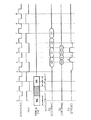
第1実施形態及び第2実施形態のメモリチップの動作は図6のタイミング図に示されている。第1実施形態の外部クロック信号CLKの周波数に比べて第1内部クロック信号CLK1の周波数はその半分に該当する。第2実施形態の第2クロック信号CLK2は第1実施形態の外部クロック信号CLKとほとんど同じ周波数を有する。アドレス信号ADDR及びコマンド信号CMDは第1内部クロック信号CLK1の上昇エッジに対してセットアップ-ホールド時間マージンを有する。半導体メモリ装置がSDR DRAMの場合、データターミナルDQを通じるデータは外部クロック信号CLKと同じ周波数を有する第2内部クロック信号CLK2の上昇エッジごとに入力または出力される。また、半導体メモリ装置がDDR DRAMの場合にはデータターミナルDQを通じて出力されるデータは第2内部クロック信号CLK2の上昇エッジと下降エッジごとに出力される。 The operation of the memory chips of the first embodiment and the second embodiment is shown in the timing diagram of FIG. The frequency of the first internal clock signal CLK1 corresponds to half of the frequency of the external clock signal CLK of the first embodiment. The second clock signal CLK2 of the second embodiment has almost the same frequency as the external clock signal CLK of the first embodiment. The address signal ADDR and the command signal CMD have a setup-hold time margin with respect to the rising edge of the first internal clock signal CLK1. When the semiconductor memory device is an SDR DRAM, data through the data terminal DQ is input or output at every rising edge of the second internal clock signal CLK2 having the same frequency as the external clock signal CLK. When the semiconductor memory device is a DDR DRAM, data output through the data terminal DQ is output at every rising edge and falling edge of the second internal clock signal CLK2.
一方、第1実施形態及び第2実施形態のメモリチップに含まれるデータバッファがデータストローブ信号STROBEに連結される場合には、データストローブ信号STROBEのエッジに応答してデータを入出力する。すなわち、図6に示したデータストローブ信号STROBEの上昇エッジと下降エッジごとにデータを出力するが、これはDDR DRAMの場合である。 On the other hand, when the data buffer included in the memory chip of the first and second embodiments is connected to the data strobe signal STROBE, data is input / output in response to the edge of the data strobe signal STROBE. That is, data is output at each rising edge and falling edge of the data strobe signal STROBE shown in FIG. 6, which is the case of DDR DRAM.
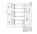
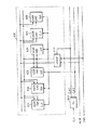
図7は、本発明の第3実施形態に係るメモリモジュール700を示す図面である。メモリモジュール700は多数のメモリチップ701、702、…、706とレジスタ710とを含む。レジスタ710はシステムボード上の第1クロック信号CLK1、アドレス信号ADDR及びコマンド信号CMDとに連結される。レジスタ710は第1クロック信号CLK1に応答して受信されるアドレス信号ADDR及びコマンド信号CMDをメモリチップ701、702、…、706に伝送する。レジスタ710から出力されるアドレス信号ADDR及びコマンド信号CMDはメモリモジュール700の一方向から各メモリチップ701、702、…、706に提供される。メモリチップ701、702、…、706はシステムボード上の第2クロック信号CLK2とレジスタ710から出力されるアドレス信号ADDR及びコマンド信号CMDとに連結される。
FIG. 7 illustrates a
一方、メモリモジュール700内のレジスタ710なしに第1クロック信号CLK1とアドレス信号ADDR、そしてコマンド信号CMDは直接メモリチップ701、702、…、706に提供されうる。この時、第1クロック信号CLK1はアドレス信号ADDRとコマンド信号CMDとを各々受信するアドレスバッファとコマンドバッファとを駆動する。そして、第2クロック信号CLK2はデータバッファを駆動する。すなわち、低い周波数の第1クロック信号CLK1はアドレス信号ADDRとコマンド信号CMDとの動作周波数として使用され、高い周波数の第2クロック信号CLK2はデータを入出力するのに使用される。
Meanwhile, the first clock signal CLK1, the address signal ADDR, and the command signal CMD may be directly provided to the
第1クロック信号CLK1、第2クロック信号CLK2、アドレス信号ADDR及びコマンド信号CMDはメモリコントローラ(図示せず)やマイクロプロセッサ(図示せず)によって提供され、システムボードを走るバスラインを通じてデバイス、特にメモリモジュール700と連結される。
The first clock signal CLK1, the second clock signal CLK2, the address signal ADDR, and the command signal CMD are provided by a memory controller (not shown) or a microprocessor (not shown), and are connected to a device, particularly a memory, through a bus line running on the system board. The
図8は本発明の第4実施形態であり、レジスタ710から出力されるアドレス信号ADDRライン及びコマンド信号CMDラインがメモリモジュール700'の中央から各メモリチップ701、702、…、706と連結される構造を示す。これは図7のメモリモジュール700内のメモリチップ701とメモリチップ706とに連結されるアドレス信号ADDR及びコマンド信号CMDのライン負荷が相異なってスキューが生じる問題点を減らす一つの方法になる。
FIG. 8 shows a fourth embodiment of the present invention. An address signal ADDR line and a command signal CMD line output from the
第1クロック信号CLK1と第2クロック信号CLK2はメモリコントローラやマイクロプロセッサにより直接提供されるが、システムボード上のシステムクロック信号CLKを受信する位相同期回路PLLにより発生させることもでき、これは本発明の第5実施形態として図9に示されている。また、本発明の第6実施形態の図10は、図9のレジスタ910から出力されるアドレス信号ADDRライン及びコマンド信号CMDラインがメモリモジュール900'の中央から各メモリチップ901、902、…、906と連結される構造を示す。
The first clock signal CLK1 and the second clock signal CLK2 are directly provided by the memory controller or the microprocessor, but may be generated by a phase synchronization circuit PLL that receives the system clock signal CLK on the system board. FIG. 9 shows the fifth embodiment. Further, FIG. 10 of the sixth embodiment of the present invention shows that the address signal ADDR line and the command signal CMD line output from the
図7ないし図10の動作はほとんど同じであるが、代表として図7を例として説明する。第1クロック信号CLK1の周波数は第2クロック信号CLK2の周波数に比べて低い。低い周波数の第1クロック信号CLK1はレジスタ710の動作クロック信号として使われ、高い周波数の第2クロック信号CLK2はメモリチップ701、702、…、706の動作クロック信号として使われる。これはメモリチップ701、702、…、706の動作速度に比べて相対的にその動作速度が遅いレジスタ710の性能に合わせたためである。メモリチップ701、702、…、706は高速動作のSDRAMより構成され、より具体的にはDDR DRAMまたはSDR DRAMなどである。
Although the operations of FIGS. 7 to 10 are almost the same, FIG. 7 will be described as an example. The frequency of the first clock signal CLK1 is lower than the frequency of the second clock signal CLK2. The first clock signal CLK1 having a low frequency is used as an operation clock signal for the
したがって、メモリモジュール700は、従来のメモリモジュールが一つのクロック信号を受信してこれをメモリモジュール全体に配分させていたこととは違って、二つのクロック信号CLK1、CLK2を受信してこれを動作周波数が異なるデバイス、すなわち、レジスタ710とメモリチップ701、702、…、706とに各々連結させる。それで、メモリモジュール700は2個のクロック信号CLK1、CLK2を受信するのに使われるモジュールピンを各々具備する。本実施形態では2個のクロック信号、すなわち、第1クロック信号CLK1と第2クロック信号CLK2とを例として説明しているが、2つ以上の相異なる周波数を有するクロック信号を受信してこれらを該当周波数別に動作するデバイス群に各々連結させうることはもちろんである。
Accordingly, the
したがって、図7ないし図10のメモリモジュール700、700'、900、900'は、メモリモジュール内の動作周波数領域が相異なるレジスタとメモリチップとが該当周波数のクロック信号に選択的に連結されるために、特に動作周波数が低いレジスタは安定して動作する。
Accordingly, in the
図11は、本発明の第7実施形態に係るメモリモジュール1100を示す図面である。メモリモジュール1100は図7のメモリモジュール700とほとんど同一である。ただし、図7のメモリモジュール700では、第2クロック信号CLK2を受信してこれをメモリチップ701、702、…、706に直接連結させるのに対して、本実施形態のメモリモジュール1100は第2クロック信号CLK2を受信してこれを位相同期回路1120に連結させるという点で差がある。説明の重複を避けるために同じ構成要素のレジスタ1110とメモリチップ1101、1102、…、1106についての説明は省略される。
FIG. 11 is a view illustrating a
位相同期回路PLL 1120は第2クロック信号CLK2を受信して多数の内部クロック信号ICLK1、ICLK2、…、ICLK6を発生させ、それぞれの内部クロック信号ICLK1、ICLK2、…、ICLK6をメモリチップ1101、1102、…、1106に連結させる。内部クロック信号ICLK1、ICLK2、…、ICLK6はスキューなしに同じスルーレートとデューティを有して理想的であり、第2クロック信号CLK2と位相が同期するために第2クロック信号CLK2の周波数を有する。したがって、内部クロック信号ICLK1、ICLK2、…、ICLK6も高い周波数を有する。
The phase
一方、本発明の第8実施形態の図12は、レジスタ1110から出力されるアドレス信号ADDRライン及びコマンド信号CMDラインがメモリモジュール1100'の中央から各メモリチップ1101、1102、…、1106と連結される構造を示す。これは図8で説明したように、図11のメモリモジュール1100内のメモリチップ1101とメモリチップ1106とに連結されるアドレス信号ADDR及びコマンド信号CMDのライン負荷が相異なってスキューが生じる問題点を減らす一つの方法になる。
On the other hand, in FIG. 12 of the eighth embodiment of the present invention, the address signal ADDR line and the command signal CMD line output from the
したがって、図11及び図12のメモリモジュールは図7ないし図10のメモリモジュール700、700'、900、900'と同じく、メモリモジュールが装着されるシステムのクロック周波数が高まってもメモリモジュール内の動作周波数領域が相異なるレジスタとメモリチップとは該当周波数のクロック信号に選択的に連結されるために安定して動作する。
Accordingly, the memory module of FIGS. 11 and 12 is the same as the
101 半導体メモリ装置
310 クロックバッファ
320 アドレスバッファ
330 コマンドバッファ
340 データバッファ
350 制御部
101
Claims (24)
前記第1クロック信号、前記第2クロック信号、前記アドレス信号、前記コマンド信号及び前記データが各々のせられるバスラインを通じて前記メモリコントローラと連結される多数の半導体メモリ装置を装着したメモリモジュールとを含むシステムにおいて、
前記半導体メモリ装置は、
前記第1クロック信号に連結され、これに応答して前記アドレス信号を受信するアドレスバッファと、
前記第1クロック信号に連結され、これに応答して前記コマンド信号を受信するコマンドバッファと、
前記第2クロック信号に連結され、これに応答してデータを入出力するデータバッファとを具備することを特徴とするシステム。 A memory controller for generating a first clock signal, a second clock signal having a frequency higher than the frequency of the first clock signal, an address signal, a command signal, and data;
A memory module including a plurality of semiconductor memory devices connected to the memory controller through bus lines on which the first clock signal, the second clock signal, the address signal, the command signal, and the data are respectively placed. In
The semiconductor memory device includes:
An address buffer coupled to the first clock signal and receiving the address signal in response thereto;
A command buffer coupled to the first clock signal and receiving the command signal in response thereto;
And a data buffer coupled to the second clock signal for inputting / outputting data in response thereto.
データストローブ信号のエッジごとに前記データを入出力することを特徴とする請求項1に記載のシステム。 The data buffer is
2. The system according to claim 1, wherein the data is input / output for each edge of the data strobe signal.
前記第1クロック信号に連結され、これに応答して前記アドレス信号を受信するアドレスバッファと、
前記第1クロック信号に連結され、これに応答して前記コマンド信号を受信するコマンドバッファと、
前記第2クロック信号に連結され、これに応答してデータを入出力するデータバッファとを具備することを特徴とするシステム。 In a system having a memory module connected to a bus line of a first clock signal, a second clock signal having a frequency higher than the frequency of the first clock signal, an address signal, and a command signal, and a plurality of memory chips are mounted, the memory Each of the chips
An address buffer coupled to the first clock signal and receiving the address signal in response thereto;
A command buffer coupled to the first clock signal and receiving the command signal in response thereto;
And a data buffer coupled to the second clock signal for inputting / outputting data in response thereto.
前記システム内に装着されるメモリコントローラまたはマイクロプロセッサから提供されることを特徴とする請求項4に記載のシステム。 The first clock signal, the second clock signal, the address signal, and the command signal are:
5. The system according to claim 4, wherein the system is provided from a memory controller or a microprocessor mounted in the system.
前記第1クロック信号及び前記第2クロック信号を受信する2つ以上のモジュールピンを具備することを特徴とする請求項4に記載のシステム。 The memory module is
5. The system of claim 4, comprising two or more module pins that receive the first clock signal and the second clock signal.
前記第1クロック信号に連結され、これに応答して前記アドレス信号及び前記コマンド信号を受信し、その出力を前記メモリモジュールの一方向に提供するレジスタと、
前記第2クロック信号に連結され、これに応答して前記レジスタから出力される前記アドレス信号及び前記コマンド信号を受信する多数のメモリチップとを具備することを特徴とするシステム。 In a system including a first clock signal, a bus line for a second clock signal having a frequency higher than the frequency of the first clock signal, an address signal, and a command signal, and a memory module connected to the bus lines, the memory module Is
A register coupled to the first clock signal, receiving the address signal and the command signal in response thereto, and providing an output thereof in one direction of the memory module;
And a plurality of memory chips connected to the second clock signal and receiving the address signal and the command signal output from the register in response to the second clock signal.
前記システム内に装着されるメモリコントローラまたはマイクロプロセッサから提供されることを特徴とする請求項7に記載のシステム。 The first clock signal, the second clock signal, the address signal, and the command signal are:
8. The system according to claim 7, wherein the system is provided from a memory controller or a microprocessor mounted in the system.
前記第1クロック信号及び前記第2クロック信号を受信する2つ以上のモジュールピンを具備することを特徴とする請求項7に記載のシステム。 The memory module is
8. The system of claim 7, further comprising two or more module pins that receive the first clock signal and the second clock signal.
前記第1クロック信号に連結され、これに応答して前記アドレス信号及び前記コマンド信号を受信し、その出力を前記メモリモジュールの中央で両方向に提供するレジスタと、
前記第2クロック信号に連結され、これに応答して前記レジスタから出力される前記アドレス信号及び前記コマンド信号を受信する多数のメモリチップとを具備することを特徴とするシステム。 In a system including a first clock signal, a bus line for a second clock signal having a frequency higher than the frequency of the first clock signal, an address signal, and a command signal, and a memory module connected to the bus lines, the memory module Is
A register coupled to the first clock signal, receiving the address signal and the command signal in response thereto, and providing the output in both directions in the center of the memory module;
And a plurality of memory chips connected to the second clock signal and receiving the address signal and the command signal output from the register in response to the second clock signal.
前記システム内に装着されるメモリコントローラまたはマイクロプロセッサから提供されることを特徴とする請求項10に記載のシステム。 The first clock signal, the second clock signal, the address signal, and the command signal are:
The system of claim 10, provided from a memory controller or microprocessor mounted in the system.
前記第1クロック信号及び前記第2クロック信号を受信する2つ以上のモジュールピンを具備することを特徴とする請求項10に記載のシステム。 The memory module is
11. The system of claim 10, comprising two or more module pins that receive the first clock signal and the second clock signal.
前記システムは、
前記システムクロック信号を受信して第1クロック信号及び前記第1クロック信号の周波数より高い周波数の第2クロック信号を発生させる位相同期回路を具備し、
前記メモリモジュールは前記第1クロック信号に連結され、これに応答して前記アドレス信号及び前記コマンド信号を受信し、その出力を前記メモリモジュールの一方向に提供するレジスタと、
前記第2クロック信号に連結され、これに応答して前記レジスタから出力される前記アドレス信号及び前記コマンド信号を受信する多数のメモリチップとを具備することを特徴とするシステム。 In a system having a memory module in which bus lines of a system clock signal, an address signal, and a command signal are arranged and connected to the bus lines,
The system
A phase synchronization circuit for receiving the system clock signal and generating a first clock signal and a second clock signal having a frequency higher than that of the first clock signal;
The memory module is coupled to the first clock signal, receives the address signal and the command signal in response thereto, and provides an output in one direction of the memory module;
And a plurality of memory chips connected to the second clock signal and receiving the address signal and the command signal output from the register in response to the second clock signal.
前記システム内に装着されるメモリコントローラまたはマイクロプロセッサから提供されることを特徴とする請求項13に記載のシステム。 The system clock signal, the address signal, and the command signal are:
14. The system of claim 13, provided from a memory controller or microprocessor mounted in the system.
前記第1クロック信号及び前記第2クロック信号を受信する2つ以上のモジュールピンを具備することを特徴とする請求項13に記載のシステム。 The memory module is
14. The system of claim 13, comprising two or more module pins that receive the first clock signal and the second clock signal.
前記システムは、
前記システムクロック信号を受信して第1クロック信号及び前記第1クロック信号の周波数より高い周波数の第2クロック信号を発生させる位相同期回路を具備し、
前記メモリモジュールは、
前記第1クロック信号に連結され、これに応答して前記アドレス信号及び前記コマンド信号を受信し、その出力を前記メモリモジュールの中央で両方向に提供するレジスタと、
前記第2クロック信号に連結され、これに応答して前記レジスタから出力された前記アドレス信号及び前記コマンド信号を受信する多数のメモリチップとを具備することを特徴とするシステム。 In a system having a memory module in which bus lines of a system clock signal, an address signal, and a command signal are arranged and connected to the bus lines,
The system
A phase synchronization circuit for receiving the system clock signal and generating a first clock signal and a second clock signal having a frequency higher than that of the first clock signal;
The memory module is
A register coupled to the first clock signal, receiving the address signal and the command signal in response thereto, and providing the output in both directions in the center of the memory module;
A system comprising: a plurality of memory chips coupled to the second clock signal and receiving the address signal and the command signal output from the register in response thereto.
前記システム内に装着されるメモリコントローラまたはマイクロプロセッサから提供されることを特徴とする請求項16に記載のシステム。 The system clock signal, the address signal, and the command signal are:
The system of claim 16, provided by a memory controller or microprocessor mounted in the system.
前記第1クロック信号及び前記第2クロック信号を受信する2つ以上のモジュールピンを具備することを特徴とする請求項16に記載のシステム。 The memory module is
The system of claim 16, comprising two or more module pins for receiving the first clock signal and the second clock signal.
前記第1クロック信号に連結され、これに応答して前記アドレス信号及び前記コマンド信号を受信し、その出力を前記メモリモジュールの一方向に提供するレジスタと、
前記第2クロック信号に連結され、これと位相同期する多数の内部クロック信号を発生させる位相同期回路と、
前記内部クロック信号に各々連結され、これに応答して前記レジスタから出力される前記アドレス信号及び前記コマンド信号を受信する多数のメモリチップとを具備することを特徴とするシステム。 In a system including a first clock signal, a bus line for a second clock signal having a frequency higher than the frequency of the first clock signal, an address signal, and a command signal, and a memory module connected to the bus lines, the memory module Is
A register coupled to the first clock signal, receiving the address signal and the command signal in response thereto, and providing an output thereof in one direction of the memory module;
A phase synchronization circuit coupled to the second clock signal for generating a number of internal clock signals that are phase synchronized with the second clock signal;
And a plurality of memory chips connected to the internal clock signal and receiving the address signal and the command signal output from the register in response to the internal clock signal.
前記システム内に装着されるメモリコントローラまたはマイクロプロセッサから提供されることを特徴とする請求項19に記載のシステム。 The first clock signal, the second clock signal, the address signal, and the command signal are:
The system of claim 19, wherein the system is provided from a memory controller or a microprocessor mounted in the system.
前記第1クロック信号及び前記第2クロック信号を受信する2つ以上のモジュールピンを具備することを特徴とする請求項19に記載のシステム。 The memory module is
20. The system of claim 19, comprising two or more module pins that receive the first clock signal and the second clock signal.
前記第1クロック信号に連結され、これに応答して前記アドレス信号及び前記コマンド信号を受信してその出力を前記メモリモジュールの中央で両方向に提供するレジスタと、
前記第2クロック信号に連結され、これと位相同期する多数の内部クロック信号を発生させる位相同期回路と、
前記内部クロック信号に各々連結され、これに応答して前記レジスタから出力される前記アドレス信号及び前記コマンド信号を受信する多数のメモリチップとを具備することを特徴とするシステム。 In a system including a first clock signal, a bus line for a second clock signal having a frequency higher than the frequency of the first clock signal, an address signal, and a command signal, and a memory module connected to the bus lines, the memory module Is
A register coupled to the first clock signal, responsively receiving the address signal and the command signal and providing its output in both directions in the center of the memory module;
A phase synchronization circuit coupled to the second clock signal for generating a number of internal clock signals that are phase synchronized with the second clock signal;
And a plurality of memory chips connected to the internal clock signal and receiving the address signal and the command signal output from the register in response to the internal clock signal.
前記システム内に装着されるメモリコントローラまたはマイクロプロセッサから提供されることを特徴とする請求項22に記載のシステム。 The first clock signal, the second clock signal, the address signal, and the command signal are:
23. The system of claim 22, wherein the system is provided from a memory controller or a microprocessor mounted in the system.
前記第1クロック信号及び前記第2クロック信号を受信する2つ以上のモジュールピンを具備することを特徴とする請求項22に記載のシステム。 The memory module is
The system of claim 22, comprising two or more module pins that receive the first clock signal and the second clock signal.
Applications Claiming Priority (4)
| Application Number | Priority Date | Filing Date | Title |
|---|---|---|---|
| KR20000052377 | 2000-09-05 | ||
| KR10-2000-0079186A KR100396885B1 (en) | 2000-09-05 | 2000-12-20 | Semiconductor memory device lowering high frequency system clock signal for the use of operation frequency of address and command and receiving different frequency clock signals, memory module and system having the same |
| KR2000P-52377 | 2000-12-20 | ||
| KR2000P-79186 | 2000-12-20 |
Related Parent Applications (1)
| Application Number | Title | Priority Date | Filing Date |
|---|---|---|---|
| JP2001267266A Division JP3960583B2 (en) | 2000-09-05 | 2001-09-04 | Semiconductor memory device and system having memory module including the same |
Publications (2)
| Publication Number | Publication Date |
|---|---|
| JP2007200542A true JP2007200542A (en) | 2007-08-09 |
| JP4700636B2 JP4700636B2 (en) | 2011-06-15 |
Family
ID=26638371
Family Applications (2)
| Application Number | Title | Priority Date | Filing Date |
|---|---|---|---|
| JP2001267266A Expired - Fee Related JP3960583B2 (en) | 2000-09-05 | 2001-09-04 | Semiconductor memory device and system having memory module including the same |
| JP2007047258A Expired - Fee Related JP4700636B2 (en) | 2000-09-05 | 2007-02-27 | System having a memory module equipped with a semiconductor memory device |
Family Applications Before (1)
| Application Number | Title | Priority Date | Filing Date |
|---|---|---|---|
| JP2001267266A Expired - Fee Related JP3960583B2 (en) | 2000-09-05 | 2001-09-04 | Semiconductor memory device and system having memory module including the same |
Country Status (6)
| Country | Link |
|---|---|
| US (1) | US6496445B2 (en) |
| JP (2) | JP3960583B2 (en) |
| CN (1) | CN1343987B (en) |
| DE (1) | DE10144247B4 (en) |
| GB (1) | GB2370667B (en) |
| TW (1) | TW530207B (en) |
Cited By (2)
| Publication number | Priority date | Publication date | Assignee | Title |
|---|---|---|---|---|
| US8054695B2 (en) | 2008-11-13 | 2011-11-08 | Hynix Semiconductor Inc. | Semiconductor memory apparatus |
| US8117363B2 (en) * | 2004-03-08 | 2012-02-14 | Samsung Electronics Co., Ltd. | Memory module capable of improving the integrity of signals transmitted through a data bus and a command/address bus, and a memory system including the same |
Families Citing this family (37)
| Publication number | Priority date | Publication date | Assignee | Title |
|---|---|---|---|---|
| JP4139579B2 (en) * | 2001-06-19 | 2008-08-27 | 株式会社ルネサステクノロジ | Semiconductor device and operation mode control method of semiconductor device |
| US6918078B2 (en) * | 2001-07-23 | 2005-07-12 | Intel Corporation | Systems with modules sharing terminations |
| US6724082B2 (en) * | 2001-07-23 | 2004-04-20 | Intel Corporation | Systems having modules with selectable on die terminations |
| US6717823B2 (en) * | 2001-07-23 | 2004-04-06 | Intel Corporation | Systems having modules with buffer chips |
| US6674648B2 (en) * | 2001-07-23 | 2004-01-06 | Intel Corporation | Termination cards and systems therefore |
| US6771515B2 (en) * | 2001-07-23 | 2004-08-03 | Intel Corporation | Systems having modules with on die terminations |
| US6674649B2 (en) * | 2001-07-23 | 2004-01-06 | Intel Corporation | Systems having modules sharing on module terminations |
| US6631083B2 (en) * | 2001-07-23 | 2003-10-07 | Intel Corporation | Systems with modules and clocking therefore |
| US6711027B2 (en) * | 2001-07-23 | 2004-03-23 | Intel Corporation | Modules having paths of different impedances |
| JP4812976B2 (en) * | 2001-07-30 | 2011-11-09 | エルピーダメモリ株式会社 | Register, memory module and memory system |
| US6944738B2 (en) * | 2002-04-16 | 2005-09-13 | Sun Microsystems, Inc. | Scalable design for DDR SDRAM buses |
| JP3838939B2 (en) | 2002-05-22 | 2006-10-25 | エルピーダメモリ株式会社 | Memory system and modules and registers |
| US6650594B1 (en) * | 2002-07-12 | 2003-11-18 | Samsung Electronics Co., Ltd. | Device and method for selecting power down exit |
| US6930953B2 (en) * | 2002-09-16 | 2005-08-16 | Texas Instruments Incorporated | Self-timed strobe generator and method for use with multi-strobe random access memories to increase memory bandwidth |
| KR100513372B1 (en) * | 2003-05-24 | 2005-09-06 | 주식회사 하이닉스반도체 | Sub-system using clock signals having different frequency for commend/address bus and data bus |
| KR100546362B1 (en) * | 2003-08-12 | 2006-01-26 | 삼성전자주식회사 | Memory controller for changing a frequency of memory clock signal selectively and method of controlling read operation of the memory using the same |
| KR100551475B1 (en) * | 2004-08-31 | 2006-02-14 | 삼성전자주식회사 | Memory module with aperiodic clock option and memory chip and hub chip for using the same |
| US7188208B2 (en) * | 2004-09-07 | 2007-03-06 | Intel Corporation | Side-by-side inverted memory address and command buses |
| KR100568546B1 (en) | 2004-10-19 | 2006-04-07 | 삼성전자주식회사 | Memory system, semiconductor memory device, and output strobe signal generating method thereof |
| KR100562655B1 (en) * | 2005-02-28 | 2006-03-20 | 주식회사 하이닉스반도체 | Driving limitation filter in semiconductor memory device and its method |
| US7339840B2 (en) * | 2005-05-13 | 2008-03-04 | Infineon Technologies Ag | Memory system and method of accessing memory chips of a memory system |
| KR100812600B1 (en) | 2005-09-29 | 2008-03-13 | 주식회사 하이닉스반도체 | Semiconductor memory device using various clock-signals of different frequency |
| US7747833B2 (en) | 2005-09-30 | 2010-06-29 | Mosaid Technologies Incorporated | Independent link and bank selection |
| US20070076502A1 (en) * | 2005-09-30 | 2007-04-05 | Pyeon Hong B | Daisy chain cascading devices |
| WO2007036050A1 (en) | 2005-09-30 | 2007-04-05 | Mosaid Technologies Incorporated | Memory with output control |
| US7652922B2 (en) | 2005-09-30 | 2010-01-26 | Mosaid Technologies Incorporated | Multiple independent serial link memory |
| US7949863B2 (en) * | 2006-03-30 | 2011-05-24 | Silicon Image, Inc. | Inter-port communication in a multi-port memory device |
| US20100169698A1 (en) * | 2008-12-25 | 2010-07-01 | Kabushiki Kaisha Toshiba | Recording medium control element, recording medium control circuit board, and recording medium control device |
| CN101923524B (en) * | 2010-08-04 | 2012-08-22 | 苏州国芯科技有限公司 | Memory interface method based on CLB (Central Logic Bus) bus |
| KR20130000241A (en) * | 2011-06-22 | 2013-01-02 | 에스케이하이닉스 주식회사 | Chip select circuit and semiconductor apparatus includng the same |
| CN103714012B (en) * | 2013-12-30 | 2016-08-17 | 龙芯中科技术有限公司 | Data processing method and device |
| KR102190962B1 (en) | 2013-12-30 | 2020-12-14 | 삼성전자주식회사 | Command processing circuit and memory device including the same |
| KR102420152B1 (en) | 2015-11-18 | 2022-07-13 | 삼성전자주식회사 | Multi-communication Device in Memory System |
| KR102641515B1 (en) * | 2016-09-19 | 2024-02-28 | 삼성전자주식회사 | Memory device and clock distribution method thereof |
| US10437514B2 (en) * | 2017-10-02 | 2019-10-08 | Micron Technology, Inc. | Apparatuses and methods including memory commands for semiconductor memories |
| US10915474B2 (en) * | 2017-11-29 | 2021-02-09 | Micron Technology, Inc. | Apparatuses and methods including memory commands for semiconductor memories |
| US11132307B2 (en) | 2018-05-25 | 2021-09-28 | Rambus Inc. | Low latency memory access |
Citations (1)
| Publication number | Priority date | Publication date | Assignee | Title |
|---|---|---|---|---|
| WO2002017323A2 (en) * | 2000-08-21 | 2002-02-28 | Micron Technology, Inc. | Synchronized write data on a high speed memory bus |
Family Cites Families (15)
| Publication number | Priority date | Publication date | Assignee | Title |
|---|---|---|---|---|
| CA1243138A (en) * | 1984-03-09 | 1988-10-11 | Masahiro Kodama | High speed memory access circuit of crt display unit |
| JP3476231B2 (en) * | 1993-01-29 | 2003-12-10 | 三菱電機エンジニアリング株式会社 | Synchronous semiconductor memory device and semiconductor memory device |
| JP2742220B2 (en) * | 1994-09-09 | 1998-04-22 | 松下電器産業株式会社 | Semiconductor storage device |
| JP3986578B2 (en) * | 1996-01-17 | 2007-10-03 | 三菱電機株式会社 | Synchronous semiconductor memory device |
| JPH1011966A (en) * | 1996-06-27 | 1998-01-16 | Mitsubishi Electric Corp | Synchronous semiconductor memory device and synchronous memory module |
| WO1998013828A1 (en) * | 1996-09-26 | 1998-04-02 | Mitsubishi Denki Kabushiki Kaisha | Synchronous type semiconductor memory device |
| US5933379A (en) * | 1996-11-18 | 1999-08-03 | Samsung Electronics, Co., Ltd. | Method and circuit for testing a semiconductor memory device operating at high frequency |
| JPH10334659A (en) | 1997-05-29 | 1998-12-18 | Mitsubishi Electric Corp | Synchronous type semiconductor storage device |
| US5978284A (en) * | 1997-08-22 | 1999-11-02 | Micron Technology, Inc. | Synchronous memory with programmable read latency |
| KR100252048B1 (en) * | 1997-11-18 | 2000-05-01 | 윤종용 | Data masking circuit and its method for semiconductor memory device |
| KR100265610B1 (en) * | 1997-12-31 | 2000-10-02 | 김영환 | Ddr sdram for increasing a data transmicssion velocity |
| JPH11213666A (en) | 1998-01-30 | 1999-08-06 | Mitsubishi Electric Corp | Output circuit and synchronous semiconductor memory device |
| JP3719934B2 (en) * | 1998-04-21 | 2005-11-24 | 松下電器産業株式会社 | Semiconductor memory device |
| JP4043151B2 (en) | 1998-08-26 | 2008-02-06 | 富士通株式会社 | High speed random accessible memory device |
| KR100301046B1 (en) * | 1998-09-01 | 2001-09-06 | 윤종용 | High speed synchronous memory device having dual ports capable of improving graphic processing speed |
-
2001
- 2001-08-22 GB GB0120457A patent/GB2370667B/en not_active Expired - Fee Related
- 2001-08-22 TW TW090120621A patent/TW530207B/en not_active IP Right Cessation
- 2001-08-30 CN CN01125164.6A patent/CN1343987B/en not_active Expired - Fee Related
- 2001-09-04 JP JP2001267266A patent/JP3960583B2/en not_active Expired - Fee Related
- 2001-09-05 DE DE10144247A patent/DE10144247B4/en not_active Expired - Fee Related
- 2001-09-05 US US09/946,166 patent/US6496445B2/en not_active Expired - Fee Related
-
2007
- 2007-02-27 JP JP2007047258A patent/JP4700636B2/en not_active Expired - Fee Related
Patent Citations (2)
| Publication number | Priority date | Publication date | Assignee | Title |
|---|---|---|---|---|
| WO2002017323A2 (en) * | 2000-08-21 | 2002-02-28 | Micron Technology, Inc. | Synchronized write data on a high speed memory bus |
| JP2004507032A (en) * | 2000-08-21 | 2004-03-04 | マイクロン テクノロジー インコーポレイテッド | Synchronous data writing on high-speed memory bus |
Cited By (3)
| Publication number | Priority date | Publication date | Assignee | Title |
|---|---|---|---|---|
| US8117363B2 (en) * | 2004-03-08 | 2012-02-14 | Samsung Electronics Co., Ltd. | Memory module capable of improving the integrity of signals transmitted through a data bus and a command/address bus, and a memory system including the same |
| US8054695B2 (en) | 2008-11-13 | 2011-11-08 | Hynix Semiconductor Inc. | Semiconductor memory apparatus |
| US8270232B2 (en) | 2008-11-13 | 2012-09-18 | Hynix Semiconductor Inc. | Semiconductor memory apparatus |
Also Published As
| Publication number | Publication date |
|---|---|
| CN1343987A (en) | 2002-04-10 |
| GB2370667A (en) | 2002-07-03 |
| US20020039324A1 (en) | 2002-04-04 |
| GB2370667B (en) | 2003-02-12 |
| JP4700636B2 (en) | 2011-06-15 |
| DE10144247B4 (en) | 2013-11-14 |
| JP3960583B2 (en) | 2007-08-15 |
| GB0120457D0 (en) | 2001-10-17 |
| CN1343987B (en) | 2010-05-05 |
| DE10144247A1 (en) | 2002-03-14 |
| TW530207B (en) | 2003-05-01 |
| US6496445B2 (en) | 2002-12-17 |
| JP2002133867A (en) | 2002-05-10 |
Similar Documents
| Publication | Publication Date | Title |
|---|---|---|
| JP4700636B2 (en) | System having a memory module equipped with a semiconductor memory device | |
| US7605631B2 (en) | Delay line synchronizer apparatus and method | |
| US20040133758A1 (en) | Memory controller, interface device and method using a mode selection signal to support different types of memories | |
| KR20030033070A (en) | System and method for providing reliable transmission in a buffered memory system | |
| JP4561782B2 (en) | Semiconductor memory device and method of operating semiconductor memory device | |
| KR20000006028A (en) | Clock latency compensation circuit for ddr timing | |
| US20070103241A1 (en) | Clock signal generating circuit, semiconductor integrated circuit and method for controlling a frequency division ratio | |
| US8406080B2 (en) | Data output control circuit of a double data rate (DDR) synchronous semiconductor memory device responsive to a delay locked loop (DLL) clock and method thereof | |
| KR20050010704A (en) | Semiconductor memory device and module for high frequency operation | |
| KR20080018135A (en) | Method and circuit for transmitting a memory clock signal | |
| JP4561783B2 (en) | Semiconductor memory device and method of operating semiconductor memory device | |
| US20090168565A1 (en) | Semiconductor memory device and method for operating the same | |
| KR100396885B1 (en) | Semiconductor memory device lowering high frequency system clock signal for the use of operation frequency of address and command and receiving different frequency clock signals, memory module and system having the same | |
| JP2005353168A (en) | Memory interface circuit and memory interface method | |
| KR20030060517A (en) | Clock synchronizing circuit for use in an integrated circuit device | |
| US7791963B2 (en) | Semiconductor memory device and operation method thereof | |
| KR100360409B1 (en) | Semiconductor memory device using dedicated command and address strobe signal and method for inputting command and address thereof | |
| US7366827B2 (en) | Method and apparatus for selectively transmitting command signal and address signal | |
| TWI238934B (en) | Memory system using non-distributed command/address clock | |
| JP3173728B2 (en) | Semiconductor device | |
| JP2008305349A (en) | Remote controller | |
| JP4843334B2 (en) | Memory control device | |
| KR100304749B1 (en) | Semiconductor storage device | |
| JP2008251060A (en) | Semiconductor memory device | |
| GB2379542A (en) | System comprising a memory module |
Legal Events
| Date | Code | Title | Description |
|---|---|---|---|
| A977 | Report on retrieval |
Free format text: JAPANESE INTERMEDIATE CODE: A971007 Effective date: 20100430 |
|
| A131 | Notification of reasons for refusal |
Free format text: JAPANESE INTERMEDIATE CODE: A131 Effective date: 20100518 |
|
| A521 | Request for written amendment filed |
Free format text: JAPANESE INTERMEDIATE CODE: A523 Effective date: 20100729 |
|
| A01 | Written decision to grant a patent or to grant a registration (utility model) |
Free format text: JAPANESE INTERMEDIATE CODE: A01 Effective date: 20110208 |
|
| A61 | First payment of annual fees (during grant procedure) |
Free format text: JAPANESE INTERMEDIATE CODE: A61 Effective date: 20110304 |
|
| LAPS | Cancellation because of no payment of annual fees |