JP2007156824A - Processor system, task control method - Google Patents
Processor system, task control method Download PDFInfo
- Publication number
- JP2007156824A JP2007156824A JP2005351012A JP2005351012A JP2007156824A JP 2007156824 A JP2007156824 A JP 2007156824A JP 2005351012 A JP2005351012 A JP 2005351012A JP 2005351012 A JP2005351012 A JP 2005351012A JP 2007156824 A JP2007156824 A JP 2007156824A
- Authority
- JP
- Japan
- Prior art keywords
- processor
- general
- processing
- task
- dedicated signal
- Prior art date
- Legal status (The legal status is an assumption and is not a legal conclusion. Google has not performed a legal analysis and makes no representation as to the accuracy of the status listed.)
- Pending
Links
Images


Classifications
-
- G—PHYSICS
- G06—COMPUTING; CALCULATING OR COUNTING
- G06F—ELECTRIC DIGITAL DATA PROCESSING
- G06F9/00—Arrangements for program control, e.g. control units
- G06F9/06—Arrangements for program control, e.g. control units using stored programs, i.e. using an internal store of processing equipment to receive or retain programs
- G06F9/30—Arrangements for executing machine instructions, e.g. instruction decode
- G06F9/38—Concurrent instruction execution, e.g. pipeline, look ahead
- G06F9/3877—Concurrent instruction execution, e.g. pipeline, look ahead using a slave processor, e.g. coprocessor
- G06F9/3879—Concurrent instruction execution, e.g. pipeline, look ahead using a slave processor, e.g. coprocessor for non-native instruction execution, e.g. executing a command; for Java instruction set
-
- G—PHYSICS
- G06—COMPUTING; CALCULATING OR COUNTING
- G06F—ELECTRIC DIGITAL DATA PROCESSING
- G06F8/00—Arrangements for software engineering
- G06F8/40—Transformation of program code
- G06F8/54—Link editing before load time
-
- G—PHYSICS
- G06—COMPUTING; CALCULATING OR COUNTING
- G06F—ELECTRIC DIGITAL DATA PROCESSING
- G06F15/00—Digital computers in general; Data processing equipment in general
- G06F15/16—Combinations of two or more digital computers each having at least an arithmetic unit, a program unit and a register, e.g. for a simultaneous processing of several programs
- G06F15/177—Initialisation or configuration control
-
- G—PHYSICS
- G06—COMPUTING; CALCULATING OR COUNTING
- G06F—ELECTRIC DIGITAL DATA PROCESSING
- G06F15/00—Digital computers in general; Data processing equipment in general
- G06F15/76—Architectures of general purpose stored program computers
- G06F15/78—Architectures of general purpose stored program computers comprising a single central processing unit
- G06F15/7839—Architectures of general purpose stored program computers comprising a single central processing unit with memory
- G06F15/7842—Architectures of general purpose stored program computers comprising a single central processing unit with memory on one IC chip (single chip microcontrollers)
-
- G—PHYSICS
- G06—COMPUTING; CALCULATING OR COUNTING
- G06F—ELECTRIC DIGITAL DATA PROCESSING
- G06F9/00—Arrangements for program control, e.g. control units
- G06F9/06—Arrangements for program control, e.g. control units using stored programs, i.e. using an internal store of processing equipment to receive or retain programs
- G06F9/30—Arrangements for executing machine instructions, e.g. instruction decode
- G06F9/38—Concurrent instruction execution, e.g. pipeline, look ahead
-
- G—PHYSICS
- G06—COMPUTING; CALCULATING OR COUNTING
- G06F—ELECTRIC DIGITAL DATA PROCESSING
- G06F9/00—Arrangements for program control, e.g. control units
- G06F9/06—Arrangements for program control, e.g. control units using stored programs, i.e. using an internal store of processing equipment to receive or retain programs
- G06F9/46—Multiprogramming arrangements
- G06F9/48—Program initiating; Program switching, e.g. by interrupt
- G06F9/4806—Task transfer initiation or dispatching
- G06F9/4843—Task transfer initiation or dispatching by program, e.g. task dispatcher, supervisor, operating system
- G06F9/485—Task life-cycle, e.g. stopping, restarting, resuming execution
-
- G—PHYSICS
- G06—COMPUTING; CALCULATING OR COUNTING
- G06F—ELECTRIC DIGITAL DATA PROCESSING
- G06F9/00—Arrangements for program control, e.g. control units
- G06F9/06—Arrangements for program control, e.g. control units using stored programs, i.e. using an internal store of processing equipment to receive or retain programs
- G06F9/46—Multiprogramming arrangements
- G06F9/50—Allocation of resources, e.g. of the central processing unit [CPU]
-
- Y—GENERAL TAGGING OF NEW TECHNOLOGICAL DEVELOPMENTS; GENERAL TAGGING OF CROSS-SECTIONAL TECHNOLOGIES SPANNING OVER SEVERAL SECTIONS OF THE IPC; TECHNICAL SUBJECTS COVERED BY FORMER USPC CROSS-REFERENCE ART COLLECTIONS [XRACs] AND DIGESTS
- Y02—TECHNOLOGIES OR APPLICATIONS FOR MITIGATION OR ADAPTATION AGAINST CLIMATE CHANGE
- Y02D—CLIMATE CHANGE MITIGATION TECHNOLOGIES IN INFORMATION AND COMMUNICATION TECHNOLOGIES [ICT], I.E. INFORMATION AND COMMUNICATION TECHNOLOGIES AIMING AT THE REDUCTION OF THEIR OWN ENERGY USE
- Y02D10/00—Energy efficient computing, e.g. low power processors, power management or thermal management
Abstract
Description
本発明は、プロセッサシステムに関し、特に、携帯電話に用いられるアプリケーションプロセッサにおける信号処理を実行するためのプロセッサ構成形態、プロセッサ間通信方法、及び各プロセッサ内で動作するタスク制御方法に関する。 The present invention relates to a processor system, and more particularly to a processor configuration form for executing signal processing in an application processor used in a mobile phone, an inter-processor communication method, and a task control method operating in each processor.
近年の携帯電話等に用いられるプロセッサシステムの形態は、1つ又は複数の汎用プロセッサと、1つ又は複数の専用信号処理用プロセッサ、又は専用信号処理用ロジックハードウエア、更に他のインターフェースロジック等の各部品を1つのLSIとして構成したものであり、その上で、データ圧縮、伸張、電話、音声生成、などのマルチメディア処理が実行されている。 The form of a processor system used in recent cellular phones and the like includes one or more general-purpose processors, one or more dedicated signal processing processors, dedicated signal processing logic hardware, and other interface logic. Each component is configured as one LSI, and multimedia processing such as data compression, decompression, telephone call, and voice generation is performed on the LSI.
上記の構成において、MPEG4などの信号処理を実行する際は、予期せぬ処理負荷増大を避けるため、通常、想定される全ての処理のメモリ配置を予め決めておき、汎用プロセッサからその処理全体を受け持つ専用信号処理用プロセッサ側へこれを事前にダウンロードしておき、要求があったときに実行する。このため、その実行中に、登録されていない処理タスクを、前記1つ又は複数の汎用プロセッサ側からの要求により、新たに追加し実行することは出来なかった。 In the above configuration, when executing signal processing such as MPEG4, in order to avoid an unexpected increase in processing load, usually, the memory arrangement of all the assumed processing is determined in advance, and the entire processing is performed from a general-purpose processor. This is downloaded in advance to the responsible dedicated signal processing processor and executed when requested. For this reason, during the execution, a processing task that is not registered cannot be newly added and executed by a request from the one or more general-purpose processors.
関連する技術として、特開平7−287702号公報(特許文献1)にディジタル信号プロセッサに関するタスク管理システム及び方法が開示されている。
この従来技術は、各機能が少なくとも1つのタスクから構成される、データ処理システム内の複数のディジタル信号プロセッサによる機能の実行を管理するためのデータ処理システムに関する。
このデータ処理システムは、データ処理動作用の中央処理装置と、前記中央処理装置に接続され、通信チャネルによって互いに接続された、複数のディジタル信号プロセッサと、ディジタル信号プロセッサ・マネージャとを含む。前記ディジタル信号プロセッサ・マネージャは、第1識別手段と、第2識別手段と、第3識別手段と、選択手段と、ロード手段と、除去手段とを含む。
第1識別手段は、ディジタル信号プロセッサのために存在するプロセッサ資源を識別する。第2識別手段は、機能がディジタル信号プロセッサにロードされることの表示に応答して、前記機能の一部を構成する、ディジタル信号プロセッサにロードされるタスクを識別する。第3識別手段は、機能が除去されることの表示に応答して、前記機能の一部を構成する、ディジタル信号プロセッサ上の、ディジタル信号プロセッサから除去されるタスクを識別する。選択手段は、第1識別手段と、追加されるタスクを識別する第2識別手段とに応答して、識別されたタスクの実行をサポートするのに十分な資源を有するディジタル信号プロセッサを選択する。ロード手段は、選択手段によるディジタル信号プロセッサの選択に応答して、ディジタル信号プロセッサ上で実行中の別の機能を構成するタスクのいずれの実行にも割り込まずに、追加すべきタスクを選択されたディジタル信号プロセッサにロードする。除去手段は、除去すべきタスクを識別する第3識別手段に応答して、ディジタル信号プロセッサ上で実行中の別の機能を構成するタスクのいずれの実行にも割り込まずに、識別されたタスクをディジタル信号プロセッサから除去する。
As a related technique, JP-A-7-287702 (Patent Document 1) discloses a task management system and method relating to a digital signal processor.
This prior art relates to a data processing system for managing the execution of functions by a plurality of digital signal processors in the data processing system, each function consisting of at least one task.
The data processing system includes a central processing unit for data processing operations, a plurality of digital signal processors connected to the central processing unit and connected to each other by a communication channel, and a digital signal processor manager. The digital signal processor manager includes first identifying means, second identifying means, third identifying means, selecting means, loading means, and removing means.
The first identification means identifies processor resources that exist for the digital signal processor. The second identification means identifies the task loaded into the digital signal processor that forms part of the function in response to an indication that the function is loaded into the digital signal processor. In response to an indication that the function is removed, the third identifying means identifies a task on the digital signal processor that is part of the function that is removed from the digital signal processor. The selection means selects a digital signal processor having sufficient resources to support execution of the identified task in response to the first identification means and the second identification means for identifying the task to be added. In response to the selection of the digital signal processor by the selection means, the loading means has selected a task to be added without interrupting any execution of tasks that constitute another function executing on the digital signal processor. Load into the digital signal processor. The removal means is responsive to the third identification means for identifying the task to be removed, and identifies the identified task without interrupting any execution of a task that constitutes another function executing on the digital signal processor. Remove from digital signal processor.
特開平5−204828号公報(特許文献2)にマルチ−メディア信号プロセッサ・コンピュータ・システムが開示されている。
このマルチ−メディア信号プロセッサ・コンピュータ・システムは、ユーザ・タスク・プログラムを実行するデジタル・プロセッサを含む。前記プログラムは信号処理要求を前記システムに出力し、要求される前記ユーザ・タスクの実行を支援し、その組み合わされる信号処理リソース要求が前記システムの使用可能な信号処理リソース能力を超過しないユーザ・タスク・プログラム要求だけを請け負うように、前記デジタル・プロセッサを適応させる手段を含むことを特徴とする。
JP-A-5-204828 (Patent Document 2) discloses a multi-media signal processor computer system.
The multi-media signal processor computer system includes a digital processor that executes a user task program. The program outputs a signal processing request to the system, supports execution of the requested user task, and the combined signal processing resource request does not exceed the available signal processing resource capability of the system -Means for adapting said digital processor to undertake only program requests.
背景技術にて示されるようなプロセッサシステム構成において、MPEG4などのメディア信号処理を、1つ又は複数の専用信号処理用プロセッサ実行するには、予期せぬ処理負荷増大を避け、一定の性能値を得るために、通常、想定される全ての処理のメモリ配置を予め決めておき、上記、汎用プロセッサからその処理全体を受け持つ専用信号処理用プロセッサ側へこれを全て事前にダウンロードしておき、要求があったときに実行する方式が取られており、その実行中に、登録されていない処理タスクを、前記1つ又は複数の汎用プロセッサ側からの要求により、新たに追加し実行することは出来なかった。また、特許文献1に開示されたプロセッサシステム構成では、同時動作するDSP(Digital Signal Processor) HW(HardWare)を複数搭載するのは、ロジック規模の増大、ハードウエアコストの増加、ひいては消費電力の増大といった問題がある。 In a processor system configuration as shown in the background art, in order to execute media signal processing such as MPEG4 by one or more dedicated signal processing processors, an unexpected increase in processing load is avoided and a constant performance value is set. In order to obtain this, usually, the memory arrangement of all the assumed processes is determined in advance, and all of these are pre-downloaded from the general-purpose processor to the dedicated signal processing processor that takes charge of the entire process. The system is executed when there is, and during the execution, it is not possible to newly add and execute a processing task that is not registered in response to a request from the one or more general-purpose processors. It was. In addition, in the processor system configuration disclosed in Patent Document 1, mounting multiple DSPs (Digital Signal Processors) HW (HardWare) that operate simultaneously increases the logic scale, hardware cost, and power consumption. There is a problem.
以下に、[発明を実施するための最良の形態]で使用される番号を括弧付きで用いて、課題を解決するための手段を説明する。これらの番号は、[特許請求の範囲]の記載と[発明を実施するための最良の形態]との対応関係を明らかにするために付加されたものである。但し、それらの番号を、[特許請求の範囲]に記載されている発明の技術的範囲の解釈に用いてはならない。 In the following, means for solving the problem will be described using the numbers used in [Best Mode for Carrying Out the Invention] in parentheses. These numbers are added to clarify the correspondence between the description of [Claims] and [Best Mode for Carrying Out the Invention]. However, these numbers should not be used to interpret the technical scope of the invention described in [Claims].
実行を要求された新規処理タスクの実行用オブジェクトを、使用されていないメモリ領域(151,161)へ配置する、少なくとも1つの汎用処理装置(110,210,310)と、
前記少なくとも1つの汎用処理装置側からの要求によりタスクの動的な生成及び消滅の管理を行い、前記新規処理タスクについて、スケジューラへの登録、及び動作中の他のタスクを含めた動作スケジューリングを行い、前記メモリ領域(151,161)から前記実行用オブジェクトを取得して前記新規処理タスクを実行する、少なくとも1つの専用信号処理装置(130)と
を具備する
プロセッサシステム。
At least one general-purpose processing device (110, 210, 310) for placing an object for execution of a new processing task requested to be executed in an unused memory area (151, 161);
Manages the dynamic generation and disappearance of tasks in response to requests from the at least one general-purpose processing device, registers the new processing tasks in the scheduler, and performs operation scheduling including other tasks in operation A processor system comprising at least one dedicated signal processing device (130) that acquires the execution object from the memory area (151, 161) and executes the new processing task.
1つ又は複数の汎用プロセッサ側における複数の処理のからの、動的な呼び出しにより、1つ又は複数の専用信号処理プロセッサ側における対応処理を適切に実行し、またその結果を適切に呼び出し元へ返却し、且つ、処理性能の変動を出来るだけ最小とする。 A dynamic call from a plurality of processes on one or a plurality of general-purpose processors appropriately executes a corresponding process on one or a plurality of dedicated signal processors, and appropriately transmits the result to a caller. Return it and minimize the variation in processing performance as much as possible.
以下に本発明の第1の実施形態について添付図面を参照して説明する。
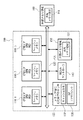
図1は、本発明のアプリケーションプロセッサの全体構成を簡易的に示したブロック図である。
本発明のアプリケーションプロセッサは、アプリケーションプロセッサ本体100、汎用CPUコア110、バス部分120、専用信号処理プロセッサコア130、割り込みコントローラ140、内部メモリ領域150を備える。また、本発明のアプリケーションプロセッサは、外部メモリ領域160と接続されている。
A first embodiment of the present invention will be described below with reference to the accompanying drawings.
FIG. 1 is a block diagram schematically showing the overall configuration of the application processor of the present invention.
The application processor of the present invention includes an application processor
アプリケーションプロセッサ本体100は、複数の汎用CPUコア110(110−i、i=1〜n:nはCPUコアの数)を持つ。汎用CPUコア110は、CPUと、PE(Processor Element)と、キャッシュメモリとを有する。バス部分120は、汎用CPUコア110、専用信号処理プロセッサコア130、割り込みコントローラ140、内部メモリ領域150を接続する。専用信号処理プロセッサコア130は、DSP(Digital Signal Processor)である。割り込みコントローラ140は、割り込み処理を行うための回路である。内部メモリ領域150は、アプリケーションプロセッサ本体100に搭載されたオンチップメモリである。外部メモリ領域160は、アプリケーションプロセッサ本体100の外部にあり、バス部分120を介して通信を行う。
The application processor
専用信号処理プロセッサコア130は、演算器コア部分131と、キャッシュ部分132とを内部に有する。演算器コア部分131は、DSPコア内ロジックであり、信号処理エンジンとなる。キャッシュ部分132は、DSPコア内キャッシュ領域であり、ここで実行される命令及びテーブルデータ等をキャッシュする役割を持つ。
The dedicated
CPU(汎用CPUコア110)とDSP(専用信号処理プロセッサコア130)の通信で使用される共有メモリ領域は、内部メモリ領域150の内部にある共有メモリ領域151、あるいは外部メモリ領域160の内部にある共有メモリ領域161、あるいはその双方に配置される。
A shared memory area used for communication between the CPU (general-purpose CPU core 110) and the DSP (dedicated signal processor core 130) is in the shared
携帯電話のアプリケーションチップのような、心臓部となるCPUを含む複合LSIは、通常CPUとDSP、また、他の様々なハードウェアロジックを含む構成となる。CPUでは、メール表示やJava(登録商標)といったメインの様々な処理を行う。DSPでは、カメラ画像の圧縮(JPEGenc/MPEG4enc)や通信相手から受信したTV画像の伸張(MPEG4dec)を行う。ここでは、CPU側が、JPEGやMPEGなどのDSPで行われるコーデックの実行オブジェクトを、DSPから実行できるようにするため、所定のRAM領域にロードする。例えば、FlashメモリからSDRAM領域へロードする。 A composite LSI including a central CPU such as an application chip of a mobile phone usually includes a CPU and a DSP, and various other hardware logics. The CPU performs various main processes such as mail display and Java (registered trademark). In the DSP, camera image compression (JPEGenc / MPEG4enc) and TV image received from a communication partner (MPEG4dec) are performed. Here, the CPU side loads an execution object of a codec performed by a DSP such as JPEG or MPEG into a predetermined RAM area so that it can be executed from the DSP. For example, the data is loaded from the flash memory to the SDRAM area.
フルキャッシュ型のDSPでは、通常のCPUのOSのようにタスク又はプロセスを増やしていくことが可能であり、これを行うためのスケジューラの機能を有している。携帯機器/小型機器用DSPに搭載するSW(SoftWare)環境は、予め実行するタスクを全て決めておき、Boot(起動)時にこれら全てを所定のメモリ上にロードする。 In a full cache type DSP, tasks or processes can be increased like a normal CPU OS, and a scheduler function is provided for this purpose. The SW (SoftWare) environment mounted on the portable device / small device DSP determines all tasks to be executed in advance, and loads all of them onto a predetermined memory at the time of Boot (activation).
DSP側OSのスケジューラは、動的に新規ディスパッチ(dispatch)されたタスクを含めてスケジューリングが可能である。なお、ディスパッチとは、実行可能なプロセスやタスクなどに対してマイクロプロセッサの計算能力を割り当てることである。 The scheduler of the DSP-side OS can perform scheduling including dynamically dispatched (dispatched) tasks. Note that dispatching assigns the computing power of a microprocessor to executable processes and tasks.
CPUとDSPとの間の通信により、CPU側からの命令をDSPへ伝え、更に、DSP側におけるCPU−DSP間の通信管理機構の働きによりDSP中で動作している各タスクに対し、CPU側からの命令を適切に配信する。 Through communication between the CPU and the DSP, a command from the CPU side is transmitted to the DSP, and further, for each task operating in the DSP by the function of the CPU-DSP communication management mechanism on the DSP side, the CPU side Properly distribute instructions from.
次に、本発明の他の実施形態について図面を参照して詳細に説明する。
図2は、本発明の第2の実施形態におけるアプリケーションプロセッサの全体構成を示す図である。
本実施形態におけるアプリケーションプロセッサは、アプリケーションプロセッサ本体100、汎用CPUコア210、バス部分120、専用信号処理プロセッサコア130、割り込みコントローラ140、内部メモリ領域150を備える。また、本発明のアプリケーションプロセッサは、外部メモリ領域160と接続されている。
Next, another embodiment of the present invention will be described in detail with reference to the drawings.
FIG. 2 is a diagram showing an overall configuration of an application processor according to the second embodiment of the present invention.
The application processor in this embodiment includes an application processor
図1と図2の違いは、汎用CPUコアである。
汎用CPUコア210は、SMP(対称型マルチプロセッサ)であり、複数のPE211(211−i、i=1〜n)と、スヌープキャッシュ212とを有する。図2では、例として、PE0(211−1),PE1(211−2),PE2(211−3)、及びスヌープキャッシュ(212)を含む構成を示している。
スヌープキャッシュでは、キャッシュ間のデータの一致制御の目的で、共有バス上のメモリアクセスを監視し、必要に応じて自キャッシュブロックに対する一貫性制御を分散的手法で行う。各プロセッサがキャッシュを持つ場合、各プロセッサがデータを取得する基本的な手順は、まず、キャッシュを検索し、キャッシュにデータが存在しない場合にはじめて共有メモリにアクセスする。
The difference between FIG. 1 and FIG. 2 is the general-purpose CPU core.
The general-
In the snoop cache, the memory access on the shared bus is monitored for the purpose of data coincidence control between caches, and the consistency control for the own cache block is performed in a distributed manner as necessary. When each processor has a cache, the basic procedure for each processor to acquire data is to first search the cache and access the shared memory only when there is no data in the cache.
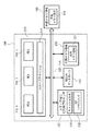
図3は、本発明の第3の実施形態におけるアプリケーションプロセッサの全体構成を示す図である。
本実施形態におけるアプリケーションプロセッサは、アプリケーションプロセッサ本体100、汎用CPUコア310、バス部分120、専用信号処理プロセッサコア130、割り込みコントローラ140、内部メモリ領域150を備える。また、本発明のアプリケーションプロセッサは、外部メモリ領域160と接続されている。
FIG. 3 is a diagram showing the overall configuration of the application processor according to the third embodiment of the present invention.
The application processor in this embodiment includes an application processor
図1と図3の違いは、汎用CPUコアである。
汎用CPUコア310は、単一CPUであり、CPUと、キャッシュメモリ311とを有する。
The difference between FIG. 1 and FIG. 3 is a general-purpose CPU core.
The general-
次に、図4のタイミング図、及び図5のフローチャートを用いて、本プロセッサシステムの動作について説明する。
図4のP101、P102、P103は、複数の汎用プロセッサ側の各CPUコアにおいて処理プロセスが動作する様子を示している。プロセスP101、P102、P103より、DSPにおける処理T101、T102、T103が呼び出される様子を示す。PE0におけるプロセスA(P101)より、対応する処理T101が呼び出され実行されるが、暫くしてPE1におけるプロセスB(P102)より、対応する処理T102を並行して呼び出し、処理T101と処理が並存する形となる。その後、処理T101は実行を終了し、これをCPU側のプロセスC(P103)へ伝え、使用していたメモリ領域は開放される。このとき、本発明の構成は図1に示すように、DSPにおいて実行されるプログラムの命令及びデータに関するキャッシュを配置しているため、このように処理内容が動的に増加しても、各処理タスクT101及びT102単体の所要性能値をそれぞれ足し合わせた値が、本DSPにて許容できる限界性能値以下であるならば、この場合における性能変動は僅かである。同様に、PE2において処理P103が実行され、これに伴い、DSP側にて対応する処理T103が呼び出され、このときDSPにおいて処理T102と処理が同時実行されるが、このときも、各処理タスクT102及びT103単体の所要性能値をそれぞれ足し合わせた値が、本DSPにて許容できる限界性能値以下であるならば、この場合における性能変動は僅かとなる。
Next, the operation of the processor system will be described with reference to the timing chart of FIG. 4 and the flowchart of FIG.
P101, P102, and P103 in FIG. 4 show how the processing process operates in each CPU core on the general-purpose processor side. The process T101, T102, T103 in the DSP is called from the processes P101, P102, P103. The corresponding process T101 is called and executed from the process A (P101) in PE0, but the corresponding process T102 is called in parallel from the process B (P102) in PE1 and the process T101 and the process coexist. It becomes a shape. Thereafter, the process T101 ends execution, and this is transmitted to the process C (P103) on the CPU side, and the used memory area is released. At this time, as shown in FIG. 1, the configuration of the present invention has a cache for instructions and data of a program executed in the DSP. If the value obtained by adding the required performance values of the tasks T101 and T102 alone is less than or equal to the limit performance value allowable in this DSP, the performance fluctuation in this case is slight. Similarly, the process P103 is executed in the PE2, and the corresponding process T103 is called on the DSP side. At this time, the process T102 and the process are simultaneously executed in the DSP. At this time, each process task T102 is also executed. If the value obtained by adding together the required performance values of T103 and T103 is less than or equal to the limit performance value allowable in this DSP, the performance fluctuation in this case will be slight.
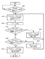
また、図5では、上記、個々のDSP処理(タスク)がCPUより呼び出され、終了するまでの流れをフローチャートで示している。
本発明における方式では、DSPにおける個々のタスクを、CPU側からの依頼に応じて個別にロードし、更に、CPU側からの処理開始コマンドを受けて、その実行を開始する。あるいは、CPU側からの処理開始コマンドを受けず、CPU側からの依頼に基づくDSP側対応実行オブジェクトのダウンロードを実行したのち、即座に処理動作を開始する形態も考えられる。また、各タスクの処理終了時は、個別にそれぞれのタスクを終了し、領域開放などの後処理を実行し、次に要求される処理に備える。
FIG. 5 is a flowchart showing the flow from when the individual DSP process (task) is called by the CPU to the end.
In the system according to the present invention, each task in the DSP is individually loaded in response to a request from the CPU side, and further, its execution is started in response to a process start command from the CPU side. Alternatively, a mode in which the processing operation is started immediately after downloading the execution object corresponding to the DSP side based on the request from the CPU side without receiving the processing start command from the CPU side is also conceivable. At the end of processing of each task, each task is individually terminated, post-processing such as area release is executed, and the next required processing is prepared.
(1)ステップS101
CPU側からDSPへの処理要求を検出する。処理要求が無ければ、処理要求があるまで待機する。
(2)ステップS102
CPU側の各プロセス(プロセスA,プロセスB,プロセスC)に対応する個々のタスクを個別にロードする。
(3)ステップS103
CPU側からコマンドを受信する。
(4)ステップS104
受信したコマンドが、CPU側の各プロセスのいずれかの処理開始コマンドである場合、ステップS105に移行する。CPU側の各プロセスのいずれかの処理開始コマンドでない場合、ステップS106に移行する。
(5)ステップS105
処理開始コマンドに対応するプロセスの実行を開始する。なお、ステップS103において、CPU側からの処理開始コマンドを受けず、CPU側からの依頼に基づくDSP側対応実行オブジェクトのダウンロードを実行したのち、即座に処理動作を開始するようにしても良い。
(6)ステップS106
受信したコマンドが、CPU側の各プロセスのいずれかの処理終了コマンドである場合、ステップS107に移行する。受信したコマンドが、CPU側の各プロセスのいずれかの処理終了コマンドでない場合、ステップS108に移行する。
(7)ステップS107
処理終了コマンドに対応するプロセスの実行を終了する。
(8)ステップS108
CPU側の各プロセスのいずれかの処理終了コマンドではない場合、受信したコマンドに対する処理を行い、ステップS102に戻る。
(1) Step S101
A processing request from the CPU side to the DSP is detected. If there is no processing request, it waits until there is a processing request.
(2) Step S102
Each task corresponding to each process (process A, process B, process C) on the CPU side is individually loaded.
(3) Step S103
A command is received from the CPU side.
(4) Step S104
When the received command is a process start command of any of the processes on the CPU side, the process proceeds to step S105. If it is not a process start command of any process on the CPU side, the process proceeds to step S106.
(5) Step S105
The execution of the process corresponding to the process start command is started. In step S103, the processing operation may be started immediately after downloading the DSP-side execution object based on the request from the CPU without receiving the processing start command from the CPU.
(6) Step S106
If the received command is a process end command of any of the processes on the CPU side, the process proceeds to step S107. If the received command is not a process end command for any of the processes on the CPU side, the process proceeds to step S108.
(7) Step S107
Terminates execution of the process corresponding to the process termination command.
(8) Step S108
If it is not a process end command of any process on the CPU side, the received command is processed, and the process returns to step S102.
なお、図2及び図3は、それぞれ、汎用プロセッサ側がSMP(対称型マルチプロセッサ)である場合、及び単一CPUだった場合の、本発明における構成を示している。この場合、それぞれ図1及び図4の場合と同じく、汎用CPUコアは、DSP側に命令及びデータ双方に関してキャッシュ機構を持つ。また、CPU側からの要求に応じて、DSP側にてタスクの個別実行を行う機構を備えている。このとき、図2に示されるSMPアーキテクチャの場合では、SMPにおいて実行されるPE番号に依存しない個々のプロセス又はスレッドよりDSPに対して処理依頼が発行され、対応されるタスクがそれぞれ独立に実行される仕組みを持つ。図3に示される単一プロセッサの場合では、CPU内にて実行される1つ又は複数のプロセス又はスレッドよりDSPに対して処理依頼が発行され、対応されるタスクがそれぞれ独立に実行される仕組みを持つ。 2 and 3 show configurations in the present invention when the general-purpose processor side is an SMP (symmetric multiprocessor) and a single CPU, respectively. In this case, as in FIGS. 1 and 4, the general-purpose CPU core has a cache mechanism for both instructions and data on the DSP side. In addition, a mechanism for individually executing tasks on the DSP side in response to a request from the CPU side is provided. At this time, in the case of the SMP architecture shown in FIG. 2, processing requests are issued to the DSP from individual processes or threads independent of the PE number executed in the SMP, and the corresponding tasks are executed independently. It has a mechanism. In the case of the single processor shown in FIG. 3, a mechanism in which a processing request is issued to the DSP from one or a plurality of processes or threads executed in the CPU, and the corresponding tasks are executed independently. have.
以上のように、本発明は、1つ又は複数の汎用プロセッサと、1つ又は複数の専用信号処理用プロセッサ、又は専用信号処理用ロジックハードウエア等の各部品を1つのLSIとして構成した、携帯電話等の用途に好適なプロセッサシステムの構成に関するものである。
このプロセッサシステムは、以下の特徴を有する。
(1)汎用プロセッサ側にて、実行を要求された新規処理タスクの実行用オブジェクトを、使用されていないメモリ領域へ新たに配置する。
(2)専用信号処理プロセッサでは、予期せぬ処理負荷の大幅な増大が起こり得ない、十分な大きさの命令キャッシュ、及びデータキャッシュを備えているものを用い、実行を要求された新規処理タスクを実行する。
(3)更に、専用信号処理プロセッサ上で稼動するOSが、汎用プロセッサ側からの要求により、タスクの動的な生成及び消滅の管理を行い、新たに追加されたタスクへのスケジューラへの登録、それまで動作していた他のタスクを含めた動作スケジューリングを行う。
(4)更に、1つ又は複数の汎用プロセッサから受領した命令を、専用信号処理プロセッサ上で動作する各タスクに配分する。この命令のフォーマットには、要求する処理内容、コマンドの送信元、結果データの送付先、及び要求内容の優先度を記録するフィールドを設けている。
As described above, the present invention is a portable device in which each component such as one or more general-purpose processors and one or more dedicated signal processing processors or dedicated signal processing logic hardware is configured as one LSI. The present invention relates to a configuration of a processor system suitable for applications such as telephones.
This processor system has the following features.
(1) On the general-purpose processor side, an object for execution of a new processing task requested to be executed is newly placed in an unused memory area.
(2) A new processing task that is requested to be executed using a dedicated signal processor that has a sufficiently large instruction cache and data cache that cannot cause an unexpected large increase in processing load. Execute.
(3) Furthermore, the OS running on the dedicated signal processor manages the dynamic generation and disappearance of tasks according to requests from the general-purpose processor, and registers the newly added tasks in the scheduler. Performs operation scheduling including other tasks that were operating until then.
(4) Further, instructions received from one or more general-purpose processors are distributed to each task operating on the dedicated signal processor. The format of this command includes fields for recording requested processing contents, command transmission source, result data transmission destination, and priority of requested contents.
本発明のプロセッサシステムでは、1つ又は複数の汎用プロセッサ側における複数の処理のからの、動的な呼び出しにより、1つ又は複数の専用信号処理プロセッサ側における対応処理を適切に実行し、またその結果を適切に呼び出し元へ返却し、且つ、処理性能の変動を出来るだけ最小とする。 In the processor system of the present invention, the corresponding processing on the one or more dedicated signal processors is appropriately executed by dynamic calling from the plurality of processes on the one or more general-purpose processors. The result is appropriately returned to the caller, and the fluctuation in processing performance is minimized as much as possible.
すなわち、プロセッサシステムにおいて、汎用プロセッサ側にて、実行を要求された新規処理タスクの実行用オブジェクトを、使用されていないメモリ領域へ新たに配置する機構を持つと共に、専用信号処理プロセッサは、予期せぬ処理負荷の大幅な増大が起こり得ない、十分な大きさの命令キャッシュ、及びデータキャッシュを備えているものを用い、実行を要求された新規処理タスクを実行する。更に、専用信号処理プロセッサ上で稼動するOSは、汎用プロセッサ側からの要求により、タスクの動的な生成及び消滅の管理を行い、新たに追加されたタスクへのスケジューラへの登録、それまで動作していた他のタスクを含めた動作スケジューリングの実行を行う。また、1つ又は複数の汎用プロセッサから受領した命令を、専用信号処理プロセッサ上で動作する各タスクに配分する機構を持つ。これにより、汎用プロセッサ側における複数の処理からの、専用信号処理プロセッサ側における対応処理を、動的な呼び出しにより実行する仕組みを提供する。 That is, in the processor system, the general-purpose processor side has a mechanism for newly arranging an execution object of a new processing task requested to be executed in an unused memory area, and the dedicated signal processing processor A new processing task requested to be executed is executed using a sufficiently large instruction cache and data cache that cannot cause a significant increase in processing load. In addition, the OS running on the dedicated signal processor manages the dynamic creation and disappearance of tasks in response to requests from the general-purpose processor, registers the newly added tasks in the scheduler, and operates until then. Execute operation scheduling including other tasks. In addition, it has a mechanism for distributing instructions received from one or more general-purpose processors to each task operating on a dedicated signal processor. This provides a mechanism for executing corresponding processing on the dedicated signal processor side from a plurality of processes on the general-purpose processor side by dynamic calling.
このため、本発明のプロセッサシステムは、これに含まれる専用信号処理プロセッサに、その内部において実行されるプログラム中の命令及びデータの双方について、その十分な量をキャッシングする手段(図1の132、図2の207、図3の305)と、1つ又は複数の汎用プロセッサにおける複数の処理のからの動的な呼び出しを、割り込み信号の発行及び共有メモリを用いたコマンドデータの受け渡しなどにより、1つ又は複数の専用信号処理プロセッサへ伝える手段(図1の151,111,140、図2の210、212、213、図3の307,312,313)と、上記専用信号処理プロセッサにおいて、汎用プロセッサから要求を受けて、タスクのロード及び実行、又は終了を、随時動的に行う手段を備える。 For this reason, the processor system of the present invention has a means for caching a sufficient amount of both instructions and data in the program executed in the dedicated signal processor included therein (132, FIG. 1). 2 (207 in FIG. 2, 305 in FIG. 3) and a dynamic call from a plurality of processes in one or a plurality of general-purpose processors by issuing an interrupt signal and passing command data using a shared memory, etc. Means (151, 111, 140 in FIG. 1, 210, 212, 213 in FIG. 2, 307, 312, 313 in FIG. 3) for transmitting to one or a plurality of dedicated signal processors, And a means for dynamically loading and executing tasks or terminating tasks as needed.
更に、複数の汎用プロセッサから、専用信号処理プロセッサに送られるコマンドデータ中において、要求する処理内容、及びコマンドの送信元、結果データの送付先、及び要求内容の優先度を記載するフィールドを設けている。 In addition, in the command data sent from a plurality of general-purpose processors to the dedicated signal processor, there are provided fields that describe the requested processing contents, the command transmission source, the result data transmission destination, and the priority of the request contents. Yes.
本発明の第1の効果は、ある時点における同時動作タスクの数が増大しても、従来構成の場合に発生する、処理性能の低下を防ぐ作用を持つというものである。これは、本プロセッサシステムにおけるキャッシング手段により、同時実行されているタスクのコード又はデータが、プロセッサからのアクセスにサイクル数を1サイクル程度しか要しないキャッシュ上に大半の場合配置されるので、キャッシュヒットミスの割合が十分小さく、なおかつキャッシュヒットミス発生時に生じる外部メモリ等へのアクセスに要するサイクル数が十分小さければ、ある時点における同時動作タスクの数が増大しても、処理性能の低下を防ぐことが出来る。 The first effect of the present invention is that even if the number of simultaneous operation tasks increases at a certain point in time, it has an action to prevent a decrease in processing performance that occurs in the conventional configuration. This is because the cache code in this processor system causes the code or data of a task that is being executed at the same time to be placed on a cache that requires only about one cycle for access from the processor. If the number of misses is sufficiently small and the number of cycles required to access external memory, etc., when a cache hit miss occurs is sufficiently small, even if the number of simultaneously operating tasks at a certain point increases, processing performance will not be degraded. I can do it.
本発明の第2の効果は、タスクのロード及び実行、又は終了を、随時動的に行う手段を備えることにより、従来の、処理を予定しているタスクをロードしておく手法では対応できなかった、予期しないタスクの処理要求に対して、これを実行し、更に結果を要求元に返却することが可能となり、無駄なメモリの消費を防ぎ、ひいては消費電力削減につなげることが出来る、というものである。 The second effect of the present invention is not supported by the conventional method of loading a task scheduled for processing by providing means for dynamically loading and executing or terminating a task as needed. In addition, it is possible to execute this in response to an unexpected task processing request, and return the result to the requester, preventing unnecessary memory consumption and thus reducing power consumption. It is.
本発明の第3の効果は、専用信号処理プロセッサに送られるコマンドデータ中に、要求する処理内容、及びコマンドの送信元、結果データの送付先、及び要求内容の優先度を記述することにより、特に複数の汎用プロセッサと専用信号処理プロセッサ間において、適切なデータの送受信を可能とすることが出来る。 According to the third effect of the present invention, by describing the requested processing content, the command transmission source, the result data transmission destination, and the priority of the requested content in the command data sent to the dedicated signal processor, In particular, it is possible to transmit and receive appropriate data between a plurality of general-purpose processors and a dedicated signal processor.
このように、本発明のプロセッサシステムにおけるキャッシング手段により、専用信号処理プロセッサにおいて、ある時点における同時動作タスクの数が増大しても、処理性能の低下を防ぐ作用を持つ。また、汎用プロセッサから要求を受けて、タスクのロード及び実行、又は終了を、随時動的に行う手段を備えることにより、従来の、処理を予定しているタスクをロードしておく手法では対応できなかった、予期しないタスクの処理要求に対して、これを実行し、結果を要求元に返却することが可能となる。更に、専用信号処理プロセッサに送られるコマンドデータ中に、前項において述べた内容を記述することにより、特に複数の汎用プロセッサと専用信号処理プロセッサ間において、適切なデータの送受信が可能となる。 As described above, the caching means in the processor system of the present invention has the effect of preventing the processing performance from being lowered even if the number of simultaneously operating tasks at a certain point increases in the dedicated signal processor. In addition, the conventional method of loading a task that is scheduled to be processed can be supported by providing a means for dynamically loading, executing, or terminating a task at any time upon receiving a request from a general-purpose processor. This can be executed in response to an unexpected task processing request that has not been received, and the result can be returned to the request source. Furthermore, by describing the contents described in the previous section in the command data sent to the dedicated signal processor, it is possible to transmit and receive appropriate data, particularly between a plurality of general-purpose processors and the dedicated signal processor.
100 アプリケーションプロセッサ
110(−i、i=1〜n) CPUコア
120 バス
130 DSP(Digital Signal Processor)コア
131 DSPコア内ロジック
132 DSPコア内キャッシュ領域
140 割り込みコントローラ
150 アプリケーションプロセッサ内メモリ(オンチップメモリ)
151 オンチップメモリ内の共有メモリ領域
160 外部メモリ
161 外部メモリ内共有メモリ領域
210 対称型マルチプロセッサコア
211(−i、i=1〜n) 対称型マルチプロセッサ内CPUコア
212 対称型マルチプロセッサ内スヌープキャッシュ
310(−i、i=1〜n) CPUコア
311 CPUコア内キャッシュメモリ
P101,P102,P103 各CPU(PE:プロセッサエレメント)にて起動されるプロセス
T101,T102,T103 CPU側の各プロセスから呼び出されるDSP側対応処理(タスク)
100 Application processor 110 (-i, i = 1 to n)
151 Shared memory area in on-
Claims (12)
前記少なくとも1つの汎用処理装置側からの要求によりタスクの動的な生成及び消滅の管理を行い、前記新規処理タスクについて、スケジューラへの登録、及び動作中の他のタスクを含めた動作スケジューリングを行い、前記メモリ領域から前記実行用オブジェクトを取得して前記新規処理タスクを実行する、少なくとも1つの専用信号処理装置と
を具備する
プロセッサシステム。 At least one general-purpose processing device that arranges an object for execution of a new processing task requested to be executed in an unused memory area;
Manages the dynamic generation and disappearance of tasks in response to requests from the at least one general-purpose processing device, registers the new processing tasks in the scheduler, and performs operation scheduling including other active tasks A processor system comprising: at least one dedicated signal processing device that acquires the execution object from the memory area and executes the new processing task.
前記命令のフォーマットは、要求する処理内容、コマンドの送信元、結果データの送付先、及び要求内容の優先度を記録するフィールドを有する
プロセッサシステム。 The processor system according to claim 1, wherein
The instruction format includes fields for recording requested processing contents, command transmission source, result data transmission destination, and priority of requested contents.
前記少なくとも1つの専用信号処理装置は、前記少なくとも1つの汎用処理装置から受領した命令に応じて前記新規処理タスクを実行する
プロセッサシステム。 The processor system according to claim 1, wherein
The at least one dedicated signal processing device executes the new processing task in response to an instruction received from the at least one general-purpose processing device.
前記少なくとも1つの汎用処理装置は、複数のプロセッサコアであり、
前記各プロセッサコアは、
CPUと、
プロセッサエレメントと、
キャッシュメモリと
を具備する
プロセッサシステム。 The processor system according to claim 1, wherein
The at least one general-purpose processing device is a plurality of processor cores;
Each of the processor cores is
CPU,
A processor element;
A processor system comprising a cache memory.
前記少なくとも1つの汎用処理装置は、SMP(対称型マルチプロセッサ)であり、
前記SMPは、
複数のプロセッサエレメントと、
スヌープキャッシュと
を具備する
プロセッサシステム。 The processor system according to claim 1, wherein
The at least one general-purpose processing device is an SMP (symmetric multiprocessor);
The SMP is
Multiple processor elements;
A processor system comprising a snoop cache.
前記少なくとも1つの汎用処理装置は、単一のプロセッサコアであり、
該プロセッサコアは、
CPUと、
キャッシュメモリと
を具備する
プロセッサシステム。 The processor system according to claim 1, wherein
The at least one general-purpose processing device is a single processor core;
The processor core is
CPU,
A processor system comprising a cache memory.
前記少なくとも1つの専用信号処理装置は、
予期せぬ処理負荷の大幅な増大が起こり得ない程度の大きさのキャッシュ領域を具備する
プロセッサシステム。 The processor system according to claim 1, wherein
The at least one dedicated signal processing device includes:
A processor system having a cache area large enough to prevent an unexpected large increase in processing load.
前記メモリ領域は、プロセッサ本体の内部に存在する
プロセッサシステム。 The processor system according to claim 1, wherein
The memory area is a processor system existing inside a processor body.
前記メモリ領域は、プロセッサ本体と接続された外部メモリの内部に存在する
プロセッサシステム。 The processor system according to claim 1, wherein
The memory area is a processor system that exists in an external memory connected to a processor main body.
(b)前記汎用プロセッサ側からコマンドを受信するステップと、
(c)前記受信したコマンドが、前記汎用プロセッサ側の各プロセスのいずれかの処理開始コマンドである場合、処理開始コマンドに対応するプロセスの実行を開始するステップと、
(d)前記受信したコマンドが、前記汎用プロセッサ側の各プロセスのいずれかの処理終了コマンドである場合、処理終了コマンドに対応するプロセスの実行を終了するステップと、
(e)前記受信したコマンドが、前記汎用プロセッサ側の各プロセスの処理開始コマンド及び処理終了コマンドのいずれでもない場合、前記受信したコマンドに対する処理を行うステップと
を具備する
タスク制御方法。 (A) individually loading each task corresponding to each process on the general-purpose processor side on the dedicated signal processor side;
(B) receiving a command from the general-purpose processor side;
(C) when the received command is a process start command of any process on the general-purpose processor side, starting execution of a process corresponding to the process start command;
(D) if the received command is a process end command of any of the processes on the general-purpose processor side, ending execution of the process corresponding to the process end command;
(E) A task control method comprising: a step of processing the received command when the received command is neither a process start command nor a process end command of each process on the general-purpose processor side.
(f)前記汎用プロセッサ側からの処理開始コマンドを受けず、前記汎用プロセッサ側からの依頼に基づき前記専用信号処理プロセッサ側で対応実行オブジェクトのダウンロードを実行した後、即座に処理動作を開始するステップと
を具備する
タスク制御方法。 (A) individually loading each task corresponding to each process on the general-purpose processor side on the dedicated signal processor side;
(F) The step of starting the processing operation immediately after downloading the corresponding execution object on the dedicated signal processing processor side based on the request from the general purpose processor side without receiving the processing start command from the general purpose processor side A task control method comprising:
(A)PE0におけるプロセスAより、専用信号処理プロセッサにおける処理タスクAが呼び出され実行されるステップと、
(B)暫くしてPE1におけるプロセスBより、前記専用信号処理プロセッサにおける処理タスクBを並行して呼び出し、前記処理タスクAと処理が並存するステップと、
(C)前記処理タスクAの実行を終了し、前記実行終了をPE2におけるプロセスCへ伝え、使用していたメモリ領域を開放するステップと
を具備する
タスク制御方法。 In the operation of the processing process of each PE (processor element) on the general-purpose processor side,
(A) a step in which processing task A in the dedicated signal processor is called and executed by the process A in PE0;
(B) After a while, the process B in the PE 1 calls the processing task B in the dedicated signal processor in parallel, and the processing task A and the process coexist.
(C) Ending the execution of the processing task A, transmitting the end of execution to the process C in PE2, and releasing the used memory area.
Priority Applications (5)
| Application Number | Priority Date | Filing Date | Title |
|---|---|---|---|
| JP2005351012A JP2007156824A (en) | 2005-12-05 | 2005-12-05 | Processor system, task control method |
| US11/607,888 US20070130446A1 (en) | 2005-12-05 | 2006-12-04 | Processor apparatus including specific signal processor core capable of dynamically scheduling tasks and its task control method |
| KR1020060122423A KR20070058995A (en) | 2005-12-05 | 2006-12-05 | Processor apparatus including specific signal processor core capable of dynamically scheduling tasks and its task control method |
| GB0624331A GB2432937B (en) | 2005-12-05 | 2006-12-05 | Processor Apparatus, Including Specific Signal Processor Core Capable of Dynamically Scheduling Tasks, and Task Control Method Therefor |
| KR1020090024095A KR20090046761A (en) | 2005-12-05 | 2009-03-20 | Processor apparatus including specific signal processor core capable of dynamically scheduling tasks and its task control method |
Applications Claiming Priority (1)
| Application Number | Priority Date | Filing Date | Title |
|---|---|---|---|
| JP2005351012A JP2007156824A (en) | 2005-12-05 | 2005-12-05 | Processor system, task control method |
Publications (2)
| Publication Number | Publication Date |
|---|---|
| JP2007156824A true JP2007156824A (en) | 2007-06-21 |
| JP2007156824A5 JP2007156824A5 (en) | 2008-04-17 |
Family
ID=37711615
Family Applications (1)
| Application Number | Title | Priority Date | Filing Date |
|---|---|---|---|
| JP2005351012A Pending JP2007156824A (en) | 2005-12-05 | 2005-12-05 | Processor system, task control method |
Country Status (4)
| Country | Link |
|---|---|
| US (1) | US20070130446A1 (en) |
| JP (1) | JP2007156824A (en) |
| KR (2) | KR20070058995A (en) |
| GB (1) | GB2432937B (en) |
Cited By (1)
| Publication number | Priority date | Publication date | Assignee | Title |
|---|---|---|---|---|
| JP2015532990A (en) * | 2012-09-27 | 2015-11-16 | インテル・コーポレーション | Processor having multiple cores, shared core extension logic, and multiple shared core extension use instructions |
Families Citing this family (24)
| Publication number | Priority date | Publication date | Assignee | Title |
|---|---|---|---|---|
| US8074248B2 (en) | 2005-07-26 | 2011-12-06 | Activevideo Networks, Inc. | System and method for providing video content associated with a source image to a television in a communication network |
| US9826197B2 (en) | 2007-01-12 | 2017-11-21 | Activevideo Networks, Inc. | Providing television broadcasts over a managed network and interactive content over an unmanaged network to a client device |
| WO2008088741A2 (en) | 2007-01-12 | 2008-07-24 | Ictv, Inc. | Interactive encoded content system including object models for viewing on a remote device |
| US9772853B1 (en) * | 2007-09-17 | 2017-09-26 | Rocket Software, Inc | Dispatching a unit of work to a specialty engine or a general processor and exception handling including continuing execution until reaching a defined exit point or restarting execution at a predefined retry point using a different engine or processor |
| AU2008304105B2 (en) * | 2007-09-27 | 2013-08-29 | Hilton, Ronald N | Apparatus, system, and method for cross-system proxy-based task offloading |
| US20090133022A1 (en) * | 2007-11-15 | 2009-05-21 | Karim Faraydon O | Multiprocessing apparatus, system and method |
| CN101471810B (en) * | 2007-12-28 | 2011-09-14 | 华为技术有限公司 | Method, device and system for implementing task in cluster circumstance |
| EP2409493A4 (en) * | 2009-03-17 | 2012-08-22 | Activevideo Networks Inc | Apparatus and methods for syndication of on-demand video |
| JP5578811B2 (en) * | 2009-06-30 | 2014-08-27 | キヤノン株式会社 | Information processing apparatus, information processing apparatus control method, and program |
| US7959061B2 (en) | 2009-09-25 | 2011-06-14 | Multi Packaging Solutions, Inc. | Folded pot cover |
| US9676511B2 (en) | 2009-09-25 | 2017-06-13 | Multi Packaging Solutions, Inc. | Foldable packaging container |
| KR101126177B1 (en) * | 2009-11-06 | 2012-03-22 | 서강대학교산학협력단 | Method and Apparatus for dynamic scheduling based on usage history, and Recording medium thereof |
| KR101653204B1 (en) * | 2010-03-16 | 2016-09-01 | 삼성전자주식회사 | System and method of dynamically task managing for data parallel processing on multi-core system |
| CA2814070A1 (en) | 2010-10-14 | 2012-04-19 | Activevideo Networks, Inc. | Streaming digital video between video devices using a cable television system |
| EP2695388B1 (en) | 2011-04-07 | 2017-06-07 | ActiveVideo Networks, Inc. | Reduction of latency in video distribution networks using adaptive bit rates |
| WO2013106390A1 (en) | 2012-01-09 | 2013-07-18 | Activevideo Networks, Inc. | Rendering of an interactive lean-backward user interface on a television |
| US9800945B2 (en) | 2012-04-03 | 2017-10-24 | Activevideo Networks, Inc. | Class-based intelligent multiplexing over unmanaged networks |
| US9123084B2 (en) | 2012-04-12 | 2015-09-01 | Activevideo Networks, Inc. | Graphical application integration with MPEG objects |
| WO2014145921A1 (en) | 2013-03-15 | 2014-09-18 | Activevideo Networks, Inc. | A multiple-mode system and method for providing user selectable video content |
| US9219922B2 (en) | 2013-06-06 | 2015-12-22 | Activevideo Networks, Inc. | System and method for exploiting scene graph information in construction of an encoded video sequence |
| US9326047B2 (en) | 2013-06-06 | 2016-04-26 | Activevideo Networks, Inc. | Overlay rendering of user interface onto source video |
| US9294785B2 (en) | 2013-06-06 | 2016-03-22 | Activevideo Networks, Inc. | System and method for exploiting scene graph information in construction of an encoded video sequence |
| CN103336756B (en) * | 2013-07-19 | 2016-01-27 | 中国人民解放军信息工程大学 | A kind of generating apparatus of data computational node |
| US9788029B2 (en) | 2014-04-25 | 2017-10-10 | Activevideo Networks, Inc. | Intelligent multiplexing using class-based, multi-dimensioned decision logic for managed networks |
Citations (4)
| Publication number | Priority date | Publication date | Assignee | Title |
|---|---|---|---|---|
| JPH06119300A (en) * | 1990-08-31 | 1994-04-28 | Texas Instr Inc <Ti> | Method and apparatus for scheduling multiprocessor system |
| JPH11259318A (en) * | 1998-03-13 | 1999-09-24 | Hitachi Ltd | Dispatch system |
| JP2002183750A (en) * | 2000-10-04 | 2002-06-28 | Terarikon Inc | Rendering system and rendering method |
| JP2002202893A (en) * | 2000-10-24 | 2002-07-19 | Texas Instruments Inc | Method for controlling execution of multiplex task and processing circuit |
Family Cites Families (21)
| Publication number | Priority date | Publication date | Assignee | Title |
|---|---|---|---|---|
| JPS63143660A (en) * | 1986-12-08 | 1988-06-15 | Fanuc Ltd | Arithmetic processor having co-processor |
| JPS63158657A (en) * | 1986-12-23 | 1988-07-01 | Fanuc Ltd | Coprocessor control system |
| US4862407A (en) * | 1987-10-05 | 1989-08-29 | Motorola, Inc. | Digital signal processing apparatus |
| GB2232514B (en) * | 1989-04-24 | 1993-09-01 | Yokogawa Electric Corp | Programmable controller |
| US6230255B1 (en) * | 1990-07-06 | 2001-05-08 | Advanced Micro Devices, Inc. | Communications processor for voice band telecommunications |
| CA2069711C (en) * | 1991-09-18 | 1999-11-30 | Donald Edward Carmon | Multi-media signal processor computer system |
| JP2516317B2 (en) * | 1992-10-13 | 1996-07-24 | インターナショナル・ビジネス・マシーンズ・コーポレイション | Data processing system and method for loading digital signal processor. |
| US5748468A (en) * | 1995-05-04 | 1998-05-05 | Microsoft Corporation | Prioritized co-processor resource manager and method |
| US6546442B1 (en) * | 1995-10-30 | 2003-04-08 | International Business Machines Corporation | Communications adapter having analog and digital interfaces for communications with remote systems |
| US5721945A (en) * | 1996-05-06 | 1998-02-24 | Advanced Micro Devices | Microprocessor configured to detect a DSP call instruction and to direct a DSP to execute a routine corresponding to the DSP call instruction |
| JP4067063B2 (en) * | 1997-11-14 | 2008-03-26 | 松下電器産業株式会社 | Microprocessor |
| US6047367A (en) * | 1998-01-20 | 2000-04-04 | International Business Machines Corporation | Microprocessor with improved out of order support |
| US6088785A (en) * | 1998-04-15 | 2000-07-11 | Diamond Multimedia Systems, Inc. | Method of configuring a functionally redefinable signal processing system |
| US20020010817A1 (en) * | 1999-01-29 | 2002-01-24 | Han-Chung Yeh | Host signal processing modem with a signal processing accelerator |
| GB2348306B (en) * | 1999-03-25 | 2003-07-30 | Ibm | Data processing systems and method for processing tasks in such systems |
| FR2792087B1 (en) * | 1999-04-07 | 2001-06-15 | Bull Sa | METHOD FOR IMPROVING THE PERFORMANCE OF A MULTIPROCESSOR SYSTEM INCLUDING A WORK WAITING LINE AND SYSTEM ARCHITECTURE FOR IMPLEMENTING THE METHOD |
| US7110417B1 (en) * | 2000-07-13 | 2006-09-19 | Nortel Networks Limited | Instance memory handoff in multi-processor systems |
| US6848110B2 (en) * | 2000-12-22 | 2005-01-25 | International Business Machines Corporation | Automatic feature augmentation for component based application programming interfaces |
| US20040172631A1 (en) * | 2001-06-20 | 2004-09-02 | Howard James E | Concurrent-multitasking processor |
| US7386326B2 (en) * | 2001-09-04 | 2008-06-10 | Texas Instruments Incorporated | Programmable task-based co-processor |
| DE10243856B4 (en) * | 2002-09-20 | 2004-09-30 | Siemens Ag | Regulator and method for operating a regulator |
-
2005
- 2005-12-05 JP JP2005351012A patent/JP2007156824A/en active Pending
-
2006
- 2006-12-04 US US11/607,888 patent/US20070130446A1/en not_active Abandoned
- 2006-12-05 GB GB0624331A patent/GB2432937B/en not_active Expired - Fee Related
- 2006-12-05 KR KR1020060122423A patent/KR20070058995A/en not_active Application Discontinuation
-
2009
- 2009-03-20 KR KR1020090024095A patent/KR20090046761A/en not_active Application Discontinuation
Patent Citations (4)
| Publication number | Priority date | Publication date | Assignee | Title |
|---|---|---|---|---|
| JPH06119300A (en) * | 1990-08-31 | 1994-04-28 | Texas Instr Inc <Ti> | Method and apparatus for scheduling multiprocessor system |
| JPH11259318A (en) * | 1998-03-13 | 1999-09-24 | Hitachi Ltd | Dispatch system |
| JP2002183750A (en) * | 2000-10-04 | 2002-06-28 | Terarikon Inc | Rendering system and rendering method |
| JP2002202893A (en) * | 2000-10-24 | 2002-07-19 | Texas Instruments Inc | Method for controlling execution of multiplex task and processing circuit |
Cited By (7)
| Publication number | Priority date | Publication date | Assignee | Title |
|---|---|---|---|---|
| JP2015532990A (en) * | 2012-09-27 | 2015-11-16 | インテル・コーポレーション | Processor having multiple cores, shared core extension logic, and multiple shared core extension use instructions |
| US9582287B2 (en) | 2012-09-27 | 2017-02-28 | Intel Corporation | Processor having multiple cores, shared core extension logic, and shared core extension utilization instructions |
| JP2017224342A (en) * | 2012-09-27 | 2017-12-21 | インテル・コーポレーション | Processor and apparatus |
| US10061593B2 (en) | 2012-09-27 | 2018-08-28 | Intel Corporation | Processor having multiple cores, shared core extension logic, and shared core extension utilization instructions |
| US10901748B2 (en) | 2012-09-27 | 2021-01-26 | Intel Corporation | Processor having multiple cores, shared core extension logic, and shared core extension utilization instructions |
| US10963263B2 (en) | 2012-09-27 | 2021-03-30 | Intel Corporation | Processor having multiple cores, shared core extension logic, and shared core extension utilization instructions |
| US11494194B2 (en) | 2012-09-27 | 2022-11-08 | Intel Corporation | Processor having multiple cores, shared core extension logic, and shared core extension utilization instructions |
Also Published As
| Publication number | Publication date |
|---|---|
| GB2432937A (en) | 2007-06-06 |
| GB2432937B (en) | 2010-03-24 |
| GB0624331D0 (en) | 2007-01-17 |
| KR20070058995A (en) | 2007-06-11 |
| KR20090046761A (en) | 2009-05-11 |
| US20070130446A1 (en) | 2007-06-07 |
Similar Documents
| Publication | Publication Date | Title |
|---|---|---|
| JP2007156824A (en) | Processor system, task control method | |
| KR101798369B1 (en) | System and method for synchronous task dispatch in a portable device | |
| JP5538442B2 (en) | Real-time multi-thread scheduler and scheduling method | |
| US10268609B2 (en) | Resource management in a multicore architecture | |
| US8972699B2 (en) | Multicore interface with dynamic task management capability and task loading and offloading method thereof | |
| JP6009529B2 (en) | Technology for setting events in a multithreaded system | |
| US8963933B2 (en) | Method for urgency-based preemption of a process | |
| US9858115B2 (en) | Task scheduling method for dispatching tasks based on computing power of different processor cores in heterogeneous multi-core processor system and related non-transitory computer readable medium | |
| JP4148223B2 (en) | Processor and information processing method | |
| US20060200826A1 (en) | Processor and information processing method | |
| JP5366552B2 (en) | Method and system for real-time execution of centralized multitasking and multiflow processing | |
| US20120173847A1 (en) | Parallel processor and method for thread processing thereof | |
| JP5673672B2 (en) | Multi-core processor system, control program, and control method | |
| KR101551321B1 (en) | Method and system for scheduling requests in a portable computing device | |
| US7366814B2 (en) | Heterogeneous multiprocessor system and OS configuration method thereof | |
| CN112465129A (en) | On-chip heterogeneous artificial intelligence processor | |
| US20090100200A1 (en) | Channel-less multithreaded DMA controller | |
| WO2012098821A1 (en) | Multiprocessor system | |
| JP2006243864A (en) | Processor and information processing method | |
| KR20140004654A (en) | Methods and systems for synchronous operation of a processing device | |
| CN103823712A (en) | Data flow processing method and device for multi-CPU virtual machine system | |
| JP2008523491A (en) | Method and system for providing access to active objects | |
| JP2005327007A (en) | Integrated computer control program, recording medium for recording its program and integrated system | |
| US20150363227A1 (en) | Data processing unit and method for operating a data processing unit | |
| WO2024037553A1 (en) | Lifecycle scheduling method and apparatus, and electronic device |
Legal Events
| Date | Code | Title | Description |
|---|---|---|---|
| A521 | Written amendment |
Free format text: JAPANESE INTERMEDIATE CODE: A523 Effective date: 20080229 |
|
| A621 | Written request for application examination |
Free format text: JAPANESE INTERMEDIATE CODE: A621 Effective date: 20081111 |
|
| A977 | Report on retrieval |
Free format text: JAPANESE INTERMEDIATE CODE: A971007 Effective date: 20100319 |
|
| A131 | Notification of reasons for refusal |
Free format text: JAPANESE INTERMEDIATE CODE: A131 Effective date: 20100326 |
|
| A521 | Written amendment |
Free format text: JAPANESE INTERMEDIATE CODE: A523 Effective date: 20100524 |
|
| A131 | Notification of reasons for refusal |
Free format text: JAPANESE INTERMEDIATE CODE: A131 Effective date: 20100827 |
|
| A521 | Written amendment |
Free format text: JAPANESE INTERMEDIATE CODE: A523 Effective date: 20101025 |
|
| A02 | Decision of refusal |
Free format text: JAPANESE INTERMEDIATE CODE: A02 Effective date: 20110628 |