JP2007149620A - Optical multi-input switch - Google Patents
Optical multi-input switch Download PDFInfo
- Publication number
- JP2007149620A JP2007149620A JP2005346265A JP2005346265A JP2007149620A JP 2007149620 A JP2007149620 A JP 2007149620A JP 2005346265 A JP2005346265 A JP 2005346265A JP 2005346265 A JP2005346265 A JP 2005346265A JP 2007149620 A JP2007149620 A JP 2007149620A
- Authority
- JP
- Japan
- Prior art keywords
- photosensor
- light guide
- mask
- light
- input switch
- Prior art date
- Legal status (The legal status is an assumption and is not a legal conclusion. Google has not performed a legal analysis and makes no representation as to the accuracy of the status listed.)
- Granted
Links
Images


Classifications
-
- G—PHYSICS
- G02—OPTICS
- G02B—OPTICAL ELEMENTS, SYSTEMS OR APPARATUS
- G02B6/00—Light guides; Structural details of arrangements comprising light guides and other optical elements, e.g. couplings
- G02B6/24—Coupling light guides
- G02B6/42—Coupling light guides with opto-electronic elements
-
- G—PHYSICS
- G01—MEASURING; TESTING
- G01C—MEASURING DISTANCES, LEVELS OR BEARINGS; SURVEYING; NAVIGATION; GYROSCOPIC INSTRUMENTS; PHOTOGRAMMETRY OR VIDEOGRAMMETRY
- G01C9/00—Measuring inclination, e.g. by clinometers, by levels
-
- G—PHYSICS
- G02—OPTICS
- G02B—OPTICAL ELEMENTS, SYSTEMS OR APPARATUS
- G02B6/00—Light guides; Structural details of arrangements comprising light guides and other optical elements, e.g. couplings
- G02B6/24—Coupling light guides
- G02B6/36—Mechanical coupling means
- G02B6/3604—Rotary joints allowing relative rotational movement between opposing fibre or fibre bundle ends
-
- G—PHYSICS
- G02—OPTICS
- G02B—OPTICAL ELEMENTS, SYSTEMS OR APPARATUS
- G02B6/00—Light guides; Structural details of arrangements comprising light guides and other optical elements, e.g. couplings
- G02B6/24—Coupling light guides
- G02B6/42—Coupling light guides with opto-electronic elements
- G02B6/4201—Packages, e.g. shape, construction, internal or external details
- G02B6/4204—Packages, e.g. shape, construction, internal or external details the coupling comprising intermediate optical elements, e.g. lenses, holograms
- G02B6/4214—Packages, e.g. shape, construction, internal or external details the coupling comprising intermediate optical elements, e.g. lenses, holograms the intermediate optical element having redirecting reflective means, e.g. mirrors, prisms for deflecting the radiation from horizontal to down- or upward direction toward a device
-
- G—PHYSICS
- G02—OPTICS
- G02B—OPTICAL ELEMENTS, SYSTEMS OR APPARATUS
- G02B6/00—Light guides; Structural details of arrangements comprising light guides and other optical elements, e.g. couplings
- G02B6/24—Coupling light guides
- G02B6/42—Coupling light guides with opto-electronic elements
- G02B6/4201—Packages, e.g. shape, construction, internal or external details
- G02B6/4249—Packages, e.g. shape, construction, internal or external details comprising arrays of active devices and fibres
- G02B6/425—Optical features
Landscapes
- Physics & Mathematics (AREA)
- General Physics & Mathematics (AREA)
- Engineering & Computer Science (AREA)
- Radar, Positioning & Navigation (AREA)
- Remote Sensing (AREA)
- Optics & Photonics (AREA)
- Switches With Compound Operations (AREA)
- Switches Operated By Changes In Physical Conditions (AREA)
Abstract
Description
本発明は、光学式多入力スイッチに関するものであり、詳しくは、光を検出媒体として光学系によって構成され、操作レバーの傾斜方向、回転角度及び昇降を検出する光学式多入力スイッチに関する。 The present invention relates to an optical multi-input switch, and more particularly, to an optical multi-input switch configured by an optical system using light as a detection medium and detecting an inclination direction, a rotation angle, and elevation of an operation lever.
従来、複数の操作手段を有する多入力スイッチには以下のようなものが提案されている。それは、図17に示すように、多入力スイッチ50の操作レバー51の押圧操作による押圧有無を検出する第1スイッチ部52と、前記操作レバー51の揺動操作による揺動方向を検出する第2スイッチ部53と、前記操作レバー51の回転操作による回転角度を検出する第3スイッチ部54とで構成されており、第1スイッチ部52には押釦スイッチ55、第2スイッチ部53にはポテンションメータ56、第3スイッチ部54にはフォトカプラ57が夫々検出用センサとして配設されている。
Conventionally, the following multi-input switches having a plurality of operation means have been proposed. As shown in FIG. 17, there are a first switch portion 52 that detects whether or not the
そして、第1スイッチ部52の検出方法は、操作レバー51の一方の端部に取付けられたノブ58を下方に押圧操作することによって操作レバー51の他方の端部に取付けられた作動杆59が降下して押釦スイッチ55をON作動させ、押圧力を解除することによってコイルバネ60の付勢力で操作レバー51が元の状態に復帰し、作動杆59が上昇して押釦スイッチ55をOFF作動させる。
And the detection method of the 1st switch part 52 is the
第2スイッチ部53の検出方法は、長孔61が形成された一対の略半円状の可動アーム62が互いに直交するように配列され、夫々の可動アーム62の両端部には軸部63が設けられてポテンションメータ56の回転軸64に固着され、夫々の長孔61が交差する位置に操作レバー51が挿通されている。そして、ノブ58を所望方向に揺動操作することによって可動アーム62に設けられた軸部63を介してポテンションメータ56の回転軸64が回転されて操作レバー51の揺動方向が検出され、揺動力を解除することによってコイルバネ60の付勢力で操作レバー51が元の状態に復帰し、可動アーム62の軸部63を介してポテンションメータ56の回転軸64が中立回転位置まで戻って該ポテンションメータ56を中立状態に復帰させる。
The detection method of the
第3スイッチ部54の検出方法は、操作レバー51の端部に設けられた作動杆59に光反射体65が形成されており、ノブ58を回転操作するとフォトカプラ57の発光部66から出射して作動杆59の光反射体65で反射された光がフォトカプラ57の受光部67で受光され、受光された光信号が回転角度検出器68に出力されて該回転角度検出器68によってそのときの操作レバー51の回転角が検出されるものである(例えば、特許文献1参照。)。
ところで、上記構成の多入力スイッチ50は、構成要素の中に機械的接点を有しているために長期間の使用に際して耐久性及び検出信頼性に問題がある。
By the way, since the
また、操作レバー51の揺動操作による揺動方向の検出については、センサとなるポテンションメータ56にその出力を電圧変換、A/D変換などの信号処理を行なう外付け部品及び回路を設ける必要があり、全体構成が複雑になってコストアップの要因となる。
In addition, regarding the detection of the swing direction by the swing operation of the
また、操作レバー51の回転操作による回転角の検出については、回転角の相対変位は検出できても基準位置に対する絶対変位は検出することができない。
In addition, regarding the detection of the rotation angle by the rotation operation of the
同様に、操作レバー51の回転操作による回転角の検出については、操作レバー51の回転速度によっては検出もれが生じ、検出精度の低下を齎す可能性がある。
Similarly, the detection of the rotation angle by the rotation operation of the
そこで、本発明は上記問題に鑑みて創案なされたもので、その目的とするところは、高い検出確度で絶対変位量が検出でき、耐久性や信頼性に優れた光学式多入力スイッチを提供することにある。 Accordingly, the present invention has been made in view of the above problems, and an object of the present invention is to provide an optical multi-input switch that can detect an absolute displacement with high detection accuracy and is excellent in durability and reliability. There is.
上記課題を解決するために、本発明の請求項1に記載された発明は、基板上に少なくとも1個のフォトセンサと、該フォトセンサを中心とする略同一円上の略等中心角度毎の位置に複数個のLEDと、前記フォトセンサを囲むように複数個の貫通孔を設けた第1のマスクとが載設され、
略平板の中央部から延びた棒部を有する導光体の棒部側に、前記導光体の略平板に略平行に遮光性の略平板の一部に光が通過するスリットを設けた第2のマスクが、前記導光体の棒部の端部に開口を有し側壁に複数の貫通孔を設けた第3のマスクが夫々一体化され、
前記フォトセンサと前記導光体の棒部端面とを対向させた状態で前記導光体の傾斜、回転及び昇降が自在に行なえるようにしたことを特徴とするものである。
In order to solve the above-mentioned problems, the invention described in
A slit that allows light to pass through a part of a substantially light-shielding substantially flat plate substantially parallel to the substantially flat plate of the light guide is provided on the rod side of the light guide having a bar portion extending from the center of the substantially flat plate. Each of the second masks is integrated with a third mask having an opening at the end of the rod portion of the light guide and having a plurality of through holes in the side wall;
The light guide can be freely tilted, rotated, and moved up and down with the photosensor and the end face of the rod of the light guide facing each other.
また、本発明の請求項2に記載された発明は、請求項1において、前記夫々のLEDは前記基板面に略垂直な方向と前記基板面に略平行で且つ前記フォトセンサに向かう方向の両方向に光軸を向けて載設され、且つ夫々のLEDは固有の変調コードに基づくパルス点灯で順次時分割点灯していることを特徴とするものである。
Further, the invention described in
また、本発明の請求項3に記載された発明は、請求項1または2のいずれか1項において、前記フォトセンサはフォトダイオード、PINフォトダイオード及びフォトトランジスタからなる群より選ばれた1つであることを特徴とするものである。 According to a third aspect of the present invention, in any one of the first or second aspect, the photosensor is one selected from the group consisting of a photodiode, a PIN photodiode, and a phototransistor. It is characterized by being.
また、本発明の請求項4に記載された発明は、請求項1〜3のいずれか1項において、前記導光体が傾斜したときに、傾斜方向の反対方向に載設された前記LEDから出射した光が前記第1のマスクに設けられた貫通穴を通過して前記フォトセンサで検出されることを特徴とするものである。
Moreover, the invention described in claim 4 of the present invention is the LED according to any one of
また、本発明の請求項5に記載された発明は、請求項1〜3のいずれか1項において、前記導光体が回転したときに前記LEDから出射した光が前記第2のマスクに設けられたスリットを通過して前記導光体内に入射し、該導光体内を導光されて前記棒部の端面から出射して前記フォトセンサで検出されることを特徴とするものである。 According to a fifth aspect of the present invention, in any one of the first to third aspects, the light emitted from the LED when the light guide rotates is provided on the second mask. The light passes through the slit, enters the light guide, is guided through the light guide, exits from the end surface of the rod portion, and is detected by the photosensor.
また、本発明の請求項6に記載された発明は、請求項1〜3のいずれか1項において前記導光体が降下したときに前記LEDから出射した光が前記第1のマスクに設けられた貫通穴及び第3のマスクに設けられた貫通孔を順次通過して前記フォトセンサで検出されることを特徴とするものである。 According to a sixth aspect of the present invention, the light emitted from the LED when the light guide body is lowered according to any one of the first to third aspects is provided in the first mask. The through-holes and the through-holes provided in the third mask are sequentially passed through and detected by the photosensor.
本発明の光学式多入力スイッチは、操作レバーを傾斜、回転及び降下させたときにフォトセンサが検出するパルス光のパルス変調コードを特定することによって傾斜方向、回転角度及び降下を検出するようにした。そのため、高い検出確度で絶対変位量が検出できると共に、スイッチ検出に係わる部分に機械的接点部がないために耐久性及び検出信頼性に優れた光学式多入力スイッチを実現できる。 The optical multi-input switch of the present invention detects the tilt direction, the rotation angle, and the descent by specifying the pulse modulation code of the pulsed light detected by the photosensor when the operation lever is tilted, rotated, and lowered. did. Therefore, an absolute displacement amount can be detected with high detection accuracy, and an optical multi-input switch excellent in durability and detection reliability can be realized because there is no mechanical contact portion in a portion related to switch detection.
以下、この発明の好適な実施形態を図1〜図16を参照しながら、詳細に説明する(同一部分については同じ符号を付す)。尚、以下に述べる実施形態は、本発明の好適な具体例であるから、技術的に好ましい種々の限定が付されているが、本発明の範囲は、以下の説明において特に本発明を限定する旨の記載がない限り、これらの実施形態に限られるものではない。 Hereinafter, preferred embodiments of the present invention will be described in detail with reference to FIGS. 1 to 16 (the same parts are denoted by the same reference numerals). The embodiments described below are preferable specific examples of the present invention, and thus various technically preferable limitations are given. However, the scope of the present invention particularly limits the present invention in the following description. Unless stated to the effect, the present invention is not limited to these embodiments.
本実施形態の主要部は、LEDとフォトセンサとを載設した基板、第1のマスク、第2のマスク、第3のマスク及び導光体で構成されている。 The main part of this embodiment is composed of a substrate on which an LED and a photosensor are mounted, a first mask, a second mask, a third mask, and a light guide.
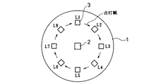
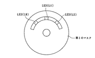
基板1は、図1に示すように略円形状の基板1上の中央部に少なくとも1つのフォトセンサ2が載設され、該フォトセンサ2を中心とする略同一円上で、略等中心角度毎の位置に8個のLED3が載設されている。
As shown in FIG. 1, the
フォトセンサ2は、フォトダイオード、PINフォトダイオード、フォトトランジスタなどの半導体受光素子からなる群の中の1つが使用されており、基板面に略垂直な方向に光軸を向けて載設されている。LED3は夫々基板面に略垂直な方向と基板面に略平行で且つフォトセンサ2に向かう方向の両方向に光軸を向けて載設されている。つまり、夫々のLED3は基板面の上方とフォトセンサ2の方向の2方向に向けて光が出射するような構成になっている。
The
基板1上に円状に載設された複数個のLED3は図2に示すようなモードで点灯する。それは、時分割方式で隣り合うLED3が1個づつ順次点灯し、それを周期的に繰り返す。また、点灯しているLED3は個々のLED3に対応した変調コードに従ってパルス点灯する。
A plurality of
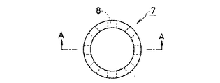
第1のマスク7は、図3及び図4(図3のA−A断面図)に示すように、両端部を開口とする略円筒形状を呈しており、基板1上にフォトセンサ2の位置と第1のマスク7の開口の中心部とを略一致させて配設したときに、第1のマスク7の外側に位置する夫々のLED3と内側に位置するフォトセンサ2とを結ぶ方向に相当する位置の8箇所側壁に所定の大きさの貫通孔8が設けてある。
As shown in FIGS. 3 and 4 (A-A cross-sectional view in FIG. 3), the
第2のマスク4は、図5及び図6(図5のA−A断面図)図3及び図4(図3のA−A断面図)に示すように、略円形状の遮光板5に部分的に光が通過するエリアを設けた構成となっている。光通過エリアの位置及び形状は、基板1と第2のマスク4とを基板1の中央部(フォトセンサ2が載設された位置)と遮光板5の中央部とを一致させて重ねたときに、基板1上に円形状に載設されたLED3に対応する位置に所定の幅を持った円弧状に形成されている。スリット6は遮光性部材からなる遮光板をスリット状にくり抜いてもよいし、透光性部材からなる透光板にスリット6以外の部分に黒色塗装などの遮光処理を施してもよい。
As shown in FIGS. 5 and 6 (cross-sectional view taken along the line AA in FIG. 5) and FIGS. 3 and 4 (cross-sectional view taken along the line AA in FIG. 3), the second mask 4 is formed on the substantially circular
第3のマスク9は、図7及び図8(図7のA−A断面図)に示すように、開口10と段付き部11を有するカップ形状を呈しており、上記基板1上に開口10を基板1側に向けて基板1上のフォトセンサ2の位置と第3のマスク9の開口10の中心部とを略一致させて配設したときに、第3のマスク9の外側に位置する夫々のLED3と内側に位置するフォトセンサ2とを結ぶ方向に相当する位置のうちの直交する位置の4箇所の側壁に所定の大きさの貫通孔12が設けてある。この場合、貫通孔12の穴位置は開口10を有しない側のカップ側壁である。
The
導光体13は、図9及び図10(図9のA−A断面図)に示すように、透光性部材からなり、略円板状の板部14の中央部に両側に向かって延びる直線状の棒部15a、15bが板部14と一体に形成されている。板部14には該板部14に導入された光を反射して進行方向を曲げるための全反射面16a、16bが設けられている。
As shown in FIGS. 9 and 10 (A-A cross-sectional view in FIG. 9), the
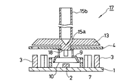
以上、本実施形態の主要部を構成する部材について説明してきたが、次に構成部材によって組み立てられた実施形態を図11を参照しながら説明する。 As mentioned above, although the member which comprises the principal part of this embodiment has been demonstrated, the embodiment assembled with the component member will be described with reference to FIG.
本発明の光学式多入力スイッチ17は略円形状の基板1上の中央部に少なくとも1つのフォトセンサ2が載設され、該フォトセンサ2を中心とする略同一円上で、略等中心角度毎の位置に8個のLED3が載設されている。更に、基板1上にはフォトセンサ2の位置と開口の中心部とを略一致させると共に、フォトセンサ2とLED3とを結ぶ位置に貫通孔8が位置するように第1のマスク7が配設されている。
In the optical
また、導光体13には、導光体13の下方に該導光体13の棒部15aを略中心とするように第2のマスク4が一体化され、導光体13の棒部15aの端部には開口10を基板1側に向けて第3のマスク9が一体化されている。導光体13の棒部15bは本スイッチを操作する操作レバーの役割を果す。
Further, the second mask 4 is integrated with the
次に、本発明の光学式多入力スイッチの操作方法と検出機構との関係について説明する。光学式多入力スイッチは操作レバーを傾ける、回転する及び降下するの3つの操作方法によって3つの検出モードが選択できる。 Next, the relationship between the operation method of the optical multi-input switch of the present invention and the detection mechanism will be described. The optical multi-input switch can select three detection modes according to three operation methods of tilting, rotating and lowering the operation lever.
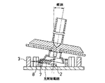
まず、操作レバーを傾ける操作をした場合の検出機構について、図12に基づいて説明する。操作レバー(棒部15b)をLED3とフォトセンサ2とを結ぶ方向のLED3と反対方向に傾けると、光軸を基板1と略平行に向けたLED3から出射した光は第1のマスク7の貫通孔8のうちの1つを通ってフォトセンサ2の方向に向かい、フォトセンサ2によって検出される。
First, the detection mechanism when the operation lever is tilted will be described with reference to FIG. When the operation lever (
この操作レバーを傾ける操作は、第1のマスク7に形成された貫通孔8の数が基板1に載設されたLED3の数と同一であるので、LED3の数と同一の検出が可能となる。本実施形態では8つのLED3を載設しているので8方向の傾き検出が可能となる。
The operation of tilting the operation lever allows the same detection as the number of
この場合、操作レバーがどの方向に傾けられたかを特定するためにはフォトセンサが検出したLED光がどのLEDから出射されたものであるかを特定すればよい。ところで、8つのLEDは上記図2で示したように、時分割で1個づつ順次点灯し、それを周期的に繰り返しており、点灯しているLEDは個々のLEDに対応した変調コードに従って発光している。よって、フォトセンサ2で検出されたLED光の変調コードを判別することによって発光源のLEDが特定でき、それによって操作レバーの傾き方向を特定することができる。
In this case, in order to specify in which direction the operation lever is tilted, it is only necessary to specify from which LED the LED light detected by the photosensor is emitted. By the way, as shown in FIG. 2 above, the eight LEDs are sequentially turned on one by one in a time-sharing manner and are periodically repeated. The lighted LEDs emit light according to the modulation codes corresponding to the individual LEDs. is doing. Therefore, by determining the modulation code of the LED light detected by the
次に、操作レバーを回転操作をした場合の検出機構について、図13〜図15に基づいて説明する。図13に示すように、LED3から出射した光は上方に配設された第2のマスク4に形成された円弧状のスリット6を通過して更にその上方に配設された導光体13内に入射する。導光体13に入射した光は導光体13内を導光されて2つの全反射面16a、16bで反射され、棒部15aの端面18からフォトセンサ2の方向に向かつて出射されてフォトセンサ2によって検出される。
Next, a detection mechanism when the operation lever is rotated will be described with reference to FIGS. As shown in FIG. 13, the light emitted from the
第2のマスク4に形成されたスリット6は、LED複数分の光が通過する長さを有しており、例えば図14で示すように3つのLED(L6、L7、L8)から出射された光がフォトセンサ2によって検出されていたものが、操作レバーを回転操作して回転角度を変えることによって図15で示すように異なる3つのLED(L1、L2、L8)から出射された光を検出するようになる。
The
従って、フォトセンサによって検出されるLED光の組み合わせを特定することによって操作レバーの回転角度を特定することができる。この場合も時分割で1個づつ順次点灯しているLEDの変調コードを判別することによって発光源となる複数のLEDの組み合わせが特定できる。 Therefore, the rotation angle of the operation lever can be specified by specifying the combination of LED light detected by the photosensor. Also in this case, a combination of a plurality of LEDs serving as a light emission source can be specified by discriminating the modulation codes of the LEDs that are sequentially turned on one by one in a time division manner.
本実施形態ではスリットを通過するLED光の組み合わせは上述の3つと4つの2つのパターンが可能である。そこで3つのLED光の組み合わせを検出する場合の操作レバーの回転角度と4つのLED光の組み合わせを検出する場合の操作レバーの回転角度とは夫々互いの中間回転角度を示すことになる。 In this embodiment, the combination of the LED light passing through the slit can be the above-described three and four two patterns. Therefore, the rotation angle of the operation lever when detecting a combination of three LED lights and the rotation angle of the operation lever when detecting a combination of four LED lights respectively indicate intermediate rotation angles.
なお、本実施形態においてはスリットは最大4つのLEDから出射した光が透過する長さで形成されているが、後述のプッシュ操作の検出を考慮すると少なくとも1つから6つのLED光が通過するような長さに形成すれば回転角度検出の機能を果すことができる。 In this embodiment, the slit is formed with a length that allows light emitted from a maximum of four LEDs to pass through. However, considering detection of a push operation described later, at least one to six LED lights pass. If it is formed to a long length, the function of detecting the rotation angle can be achieved.
次に、操作レバーを降下操作をした場合の検出機構について、図16に基づいて説明する。操作レバーを降下して第3のマスク9の開口端部19が基板1に当接した状態を保持する。すると、直交する位置に載設されて光軸を基板1と略平行に向けた4つのLED3から出射した夫々の光は第1のマスク7の貫通孔8を通過し、更に第3のマスク9の貫通孔12を通過して第3のマスク9内に入り、フォトセンサ2によって検出される。
Next, the detection mechanism when the operation lever is lowered will be described with reference to FIG. The operation lever is lowered to keep the opening
従って、フォトセンサ2が検出したLED光に上記4つのLED3から出射した光が全て存在することが検知されると、操作レバーが降下操作されていることになる。
Therefore, when it is detected that all the light emitted from the four
以上説明したように、本発明の光学式多入力スイッチは検出媒体にLED光のみを使用しているためにスイッチ検出に係わる部分に機械的接点部がなく、耐久性及び検出信頼性に優れている。 As described above, the optical multi-input switch according to the present invention uses only LED light as a detection medium, so there is no mechanical contact in the part related to switch detection, and it has excellent durability and detection reliability. Yes.
また、夫々のLEDを個別の変調コードによって時分割で順次点灯するようにしている。よって、フォトセンサで検出されるLED光の組み合わせを変調コードに基づいて特定することによってスイッチ操作の状態を検知することができる。そのとき、変調コードの特定は本体装置に搭載されたCPUのソフトウエア上で行なうことができるために外付け部品及び回路を設ける必要がなく、装置全体を低コストで製造することができる。 In addition, each LED is sequentially turned on in a time-sharing manner with individual modulation codes. Therefore, the switch operation state can be detected by specifying the combination of LED lights detected by the photosensor based on the modulation code. At this time, since the modulation code can be specified on the software of the CPU mounted on the main unit, there is no need to provide external parts and circuits, and the entire apparatus can be manufactured at low cost.
また、フォトセンサで検出されるLED光の変調コードを特定することによってどの位置に載設されたLEDから出射した光かを特定することができる。よって、回転操作による回転角度の検出を絶対角度で検出することができる。また、検出媒体が光であるために検出速度が速く、回転操作の速度に係わらず確度の高い検出を確保することができる。 Further, by specifying the modulation code of the LED light detected by the photosensor, it is possible to specify the light emitted from the LED mounted at which position. Therefore, the detection of the rotation angle by the rotation operation can be detected by an absolute angle. Further, since the detection medium is light, the detection speed is high, and detection with high accuracy can be ensured regardless of the speed of the rotation operation.
更に、スイッチの検出機構と操作時の感触(フィーリング)とは関連性がないため、操作性に関する設計の自由度が確保できる。また、組み付け精度も緩和でき、製造コストの低減に繋がる。 Furthermore, since there is no relationship between the switch detection mechanism and the feel during operation, it is possible to secure a degree of freedom in design related to operability. Moreover, assembly accuracy can be relaxed, leading to a reduction in manufacturing cost.
なお、検出媒体となるLED光を、同時にスイッチ部の照明光として活用することも可能である。 In addition, it is also possible to utilize LED light used as a detection medium as illumination light for the switch unit at the same time.
1 基板
2 フォトセンサ
3 LED
4 第2のマスク
5 遮光板
6 スリット
7 第1のマスク
8 貫通孔
9 第3のマスク
10 開口
11 段付き部
12 貫通孔
13 導光体
14 板部
15a、15b 棒部
16a、16b 全反射面
17 光学式多入力スイッチ
18 端面
19 開口端部
1
4
Claims (6)
略平板の中央部から延びた棒部を有する導光体の棒部側に、前記導光体の略平板に略平行に遮光性の略平板の一部に光が通過するスリットを設けた第2のマスクが、前記導光体の棒部の端部に開口を有し側壁に複数の貫通孔を設けた第3のマスクが夫々一体化され、
前記フォトセンサと前記導光体の棒部端面とを対向させた状態で前記導光体の傾斜、回転及び昇降が自在に行なえるようにしたことを特徴とする光学式多入力スイッチ。 At least one photosensor on the substrate, a plurality of LEDs at substantially equal center angles on substantially the same circle centered on the photosensor, and a plurality of through holes so as to surround the photosensor. A first mask provided is placed;
A slit that allows light to pass through a part of a substantially light-shielding substantially flat plate substantially parallel to the substantially flat plate of the light guide is provided on the rod side of the light guide having a bar portion extending from the center of the substantially flat plate. Each of the second masks is integrated with a third mask having an opening at the end of the rod portion of the light guide and having a plurality of through holes in the side wall;
An optical multi-input switch characterized in that the light guide can be freely tilted, rotated, and moved up and down with the photosensor and the end face of the rod of the light guide facing each other.
Priority Applications (2)
| Application Number | Priority Date | Filing Date | Title |
|---|---|---|---|
| JP2005346265A JP4739932B2 (en) | 2005-11-30 | 2005-11-30 | Optical multi-input switch |
| US11/565,064 US7292741B2 (en) | 2005-11-30 | 2006-11-30 | Multi-input optical switch |
Applications Claiming Priority (1)
| Application Number | Priority Date | Filing Date | Title |
|---|---|---|---|
| JP2005346265A JP4739932B2 (en) | 2005-11-30 | 2005-11-30 | Optical multi-input switch |
Publications (2)
| Publication Number | Publication Date |
|---|---|
| JP2007149620A true JP2007149620A (en) | 2007-06-14 |
| JP4739932B2 JP4739932B2 (en) | 2011-08-03 |
Family
ID=38087625
Family Applications (1)
| Application Number | Title | Priority Date | Filing Date |
|---|---|---|---|
| JP2005346265A Expired - Fee Related JP4739932B2 (en) | 2005-11-30 | 2005-11-30 | Optical multi-input switch |
Country Status (2)
| Country | Link |
|---|---|
| US (1) | US7292741B2 (en) |
| JP (1) | JP4739932B2 (en) |
Cited By (25)
| Publication number | Priority date | Publication date | Assignee | Title |
|---|---|---|---|---|
| JP2008186657A (en) * | 2007-01-29 | 2008-08-14 | Tokai Rika Co Ltd | Lever combination switch |
| JP2010015881A (en) * | 2008-07-04 | 2010-01-21 | Tokai Rika Co Ltd | Optical switch |
| WO2011153579A2 (en) * | 2010-06-08 | 2011-12-15 | Winelight Pty Ltd | Illuminator |
| KR20180126630A (en) * | 2013-06-11 | 2018-11-27 | 애플 인크. | Rotary input mechanism for an electronic device |
| US10331081B2 (en) | 2013-08-09 | 2019-06-25 | Apple Inc. | Tactile switch for an electronic device |
| US10509486B2 (en) | 2016-07-15 | 2019-12-17 | Apple Inc. | Capacitive gap sensor ring for an electronic watch |
| US10551798B1 (en) | 2016-05-17 | 2020-02-04 | Apple Inc. | Rotatable crown for an electronic device |
| US10572053B2 (en) | 2016-07-25 | 2020-02-25 | Apple Inc. | Force-detecting input structure |
| US10579090B2 (en) | 2016-02-27 | 2020-03-03 | Apple Inc. | Rotatable input mechanism having adjustable output |
| US10599101B2 (en) | 2014-09-02 | 2020-03-24 | Apple Inc. | Wearable electronic device |
| US10613685B2 (en) | 2014-02-12 | 2020-04-07 | Apple Inc. | Rejection of false turns of rotary inputs for electronic devices |
| US10655988B2 (en) | 2015-03-05 | 2020-05-19 | Apple Inc. | Watch with rotatable optical encoder having a spindle defining an array of alternating regions extending along an axial direction parallel to the axis of a shaft |
| US10664074B2 (en) | 2017-06-19 | 2020-05-26 | Apple Inc. | Contact-sensitive crown for an electronic watch |
| US10845764B2 (en) | 2015-03-08 | 2020-11-24 | Apple Inc. | Compressible seal for rotatable and translatable input mechanisms |
| US10962935B1 (en) | 2017-07-18 | 2021-03-30 | Apple Inc. | Tri-axis force sensor |
| US11015960B2 (en) | 2014-07-16 | 2021-05-25 | Apple Inc. | Optical encoder for detecting crown movement |
| US11181863B2 (en) | 2018-08-24 | 2021-11-23 | Apple Inc. | Conductive cap for watch crown |
| US11194298B2 (en) | 2018-08-30 | 2021-12-07 | Apple Inc. | Crown assembly for an electronic watch |
| US11194299B1 (en) | 2019-02-12 | 2021-12-07 | Apple Inc. | Variable frictional feedback device for a digital crown of an electronic watch |
| US11360440B2 (en) | 2018-06-25 | 2022-06-14 | Apple Inc. | Crown for an electronic watch |
| US11531306B2 (en) | 2013-06-11 | 2022-12-20 | Apple Inc. | Rotary input mechanism for an electronic device |
| US11550268B2 (en) | 2020-06-02 | 2023-01-10 | Apple Inc. | Switch module for electronic crown assembly |
| US11561515B2 (en) | 2018-08-02 | 2023-01-24 | Apple Inc. | Crown for an electronic watch |
| US11796968B2 (en) | 2018-08-30 | 2023-10-24 | Apple Inc. | Crown assembly for an electronic watch |
| US11796961B2 (en) | 2018-08-24 | 2023-10-24 | Apple Inc. | Conductive cap for watch crown |
Families Citing this family (6)
| Publication number | Priority date | Publication date | Assignee | Title |
|---|---|---|---|---|
| JP2005259329A (en) * | 2004-02-12 | 2005-09-22 | Sony Corp | Tilt control method and optical disc apparatus |
| US9518815B2 (en) * | 2008-08-06 | 2016-12-13 | Haas Automation, Inc. | Rotary position encoder for rotatable shafts |
| TWI494072B (en) * | 2011-12-23 | 2015-08-01 | Hon Hai Prec Ind Co Ltd | Electronic censer and its electronic incense |
| US10018966B2 (en) | 2015-04-24 | 2018-07-10 | Apple Inc. | Cover member for an input mechanism of an electronic device |
| TWI734458B (en) * | 2020-04-29 | 2021-07-21 | 群光電子股份有限公司 | Mouse device |
| US11635786B2 (en) | 2020-06-11 | 2023-04-25 | Apple Inc. | Electronic optical sensing device |
Citations (6)
| Publication number | Priority date | Publication date | Assignee | Title |
|---|---|---|---|---|
| JPS4953262U (en) * | 1972-08-16 | 1974-05-11 | ||
| JPS4953262A (en) * | 1972-07-11 | 1974-05-23 | ||
| JPH05324186A (en) * | 1992-05-18 | 1993-12-07 | Hosiden Corp | Pointing device |
| JPH11317131A (en) * | 1998-04-30 | 1999-11-16 | Japan Aviation Electronics Ind Ltd | Rotary pulse generator |
| JP2002163963A (en) * | 2000-11-24 | 2002-06-07 | Stanley Electric Co Ltd | Optical type touch switch |
| JP2004014448A (en) * | 2002-06-11 | 2004-01-15 | Alps Electric Co Ltd | Photodetection type multi-way switch |
Family Cites Families (3)
| Publication number | Priority date | Publication date | Assignee | Title |
|---|---|---|---|---|
| JPH0555433A (en) | 1991-08-27 | 1993-03-05 | Nec Corp | Semiconductor device |
| US5903000A (en) * | 1997-03-31 | 1999-05-11 | Honeywell Inc. | Method for determining the position of a rotating shaft |
| JP2000010027A (en) * | 1998-06-18 | 2000-01-14 | Alps Electric Co Ltd | Optical switch and optical communication device using the same |
-
2005
- 2005-11-30 JP JP2005346265A patent/JP4739932B2/en not_active Expired - Fee Related
-
2006
- 2006-11-30 US US11/565,064 patent/US7292741B2/en not_active Expired - Fee Related
Patent Citations (6)
| Publication number | Priority date | Publication date | Assignee | Title |
|---|---|---|---|---|
| JPS4953262A (en) * | 1972-07-11 | 1974-05-23 | ||
| JPS4953262U (en) * | 1972-08-16 | 1974-05-11 | ||
| JPH05324186A (en) * | 1992-05-18 | 1993-12-07 | Hosiden Corp | Pointing device |
| JPH11317131A (en) * | 1998-04-30 | 1999-11-16 | Japan Aviation Electronics Ind Ltd | Rotary pulse generator |
| JP2002163963A (en) * | 2000-11-24 | 2002-06-07 | Stanley Electric Co Ltd | Optical type touch switch |
| JP2004014448A (en) * | 2002-06-11 | 2004-01-15 | Alps Electric Co Ltd | Photodetection type multi-way switch |
Cited By (53)
| Publication number | Priority date | Publication date | Assignee | Title |
|---|---|---|---|---|
| JP2008186657A (en) * | 2007-01-29 | 2008-08-14 | Tokai Rika Co Ltd | Lever combination switch |
| JP2010015881A (en) * | 2008-07-04 | 2010-01-21 | Tokai Rika Co Ltd | Optical switch |
| WO2011153579A2 (en) * | 2010-06-08 | 2011-12-15 | Winelight Pty Ltd | Illuminator |
| WO2011153579A3 (en) * | 2010-06-08 | 2012-02-23 | Winelight Pty Ltd | Illuminator |
| KR20180126630A (en) * | 2013-06-11 | 2018-11-27 | 애플 인크. | Rotary input mechanism for an electronic device |
| KR102040426B1 (en) * | 2013-06-11 | 2019-11-04 | 애플 인크. | Rotary input mechanism for an electronic device |
| US11531306B2 (en) | 2013-06-11 | 2022-12-20 | Apple Inc. | Rotary input mechanism for an electronic device |
| US10331081B2 (en) | 2013-08-09 | 2019-06-25 | Apple Inc. | Tactile switch for an electronic device |
| US10331082B2 (en) | 2013-08-09 | 2019-06-25 | Apple Inc. | Tactile switch for an electronic device |
| US11886149B2 (en) | 2013-08-09 | 2024-01-30 | Apple Inc. | Tactile switch for an electronic device |
| US10962930B2 (en) | 2013-08-09 | 2021-03-30 | Apple Inc. | Tactile switch for an electronic device |
| US10732571B2 (en) | 2013-08-09 | 2020-08-04 | Apple Inc. | Tactile switch for an electronic device |
| US11669205B2 (en) | 2014-02-12 | 2023-06-06 | Apple Inc. | Rejection of false turns of rotary inputs for electronic devices |
| US10613685B2 (en) | 2014-02-12 | 2020-04-07 | Apple Inc. | Rejection of false turns of rotary inputs for electronic devices |
| US10884549B2 (en) | 2014-02-12 | 2021-01-05 | Apple Inc. | Rejection of false turns of rotary inputs for electronic devices |
| US11347351B2 (en) | 2014-02-12 | 2022-05-31 | Apple Inc. | Rejection of false turns of rotary inputs for electronic devices |
| US11015960B2 (en) | 2014-07-16 | 2021-05-25 | Apple Inc. | Optical encoder for detecting crown movement |
| US10599101B2 (en) | 2014-09-02 | 2020-03-24 | Apple Inc. | Wearable electronic device |
| US11474483B2 (en) | 2014-09-02 | 2022-10-18 | Apple Inc. | Wearable electronic device |
| US10627783B2 (en) | 2014-09-02 | 2020-04-21 | Apple Inc. | Wearable electronic device |
| US10620591B2 (en) | 2014-09-02 | 2020-04-14 | Apple Inc. | Wearable electronic device |
| US10613485B2 (en) | 2014-09-02 | 2020-04-07 | Apple Inc. | Wearable electronic device |
| US10942491B2 (en) | 2014-09-02 | 2021-03-09 | Apple Inc. | Wearable electronic device |
| US11221590B2 (en) | 2014-09-02 | 2022-01-11 | Apple Inc. | Wearable electronic device |
| US11567457B2 (en) | 2014-09-02 | 2023-01-31 | Apple Inc. | Wearable electronic device |
| US11762342B2 (en) | 2014-09-02 | 2023-09-19 | Apple Inc. | Wearable electronic device |
| US11002572B2 (en) | 2015-03-05 | 2021-05-11 | Apple Inc. | Optical encoder with direction-dependent optical properties comprising a spindle having an array of surface features defining a concave contour along a first direction and a convex contour along a second direction |
| US10655988B2 (en) | 2015-03-05 | 2020-05-19 | Apple Inc. | Watch with rotatable optical encoder having a spindle defining an array of alternating regions extending along an axial direction parallel to the axis of a shaft |
| US10845764B2 (en) | 2015-03-08 | 2020-11-24 | Apple Inc. | Compressible seal for rotatable and translatable input mechanisms |
| US11988995B2 (en) | 2015-03-08 | 2024-05-21 | Apple Inc. | Compressible seal for rotatable and translatable input mechanisms |
| US10579090B2 (en) | 2016-02-27 | 2020-03-03 | Apple Inc. | Rotatable input mechanism having adjustable output |
| US10551798B1 (en) | 2016-05-17 | 2020-02-04 | Apple Inc. | Rotatable crown for an electronic device |
| US11513613B2 (en) | 2016-07-15 | 2022-11-29 | Apple Inc. | Capacitive gap sensor ring for an input device |
| US10955937B2 (en) | 2016-07-15 | 2021-03-23 | Apple Inc. | Capacitive gap sensor ring for an input device |
| US10509486B2 (en) | 2016-07-15 | 2019-12-17 | Apple Inc. | Capacitive gap sensor ring for an electronic watch |
| US10572053B2 (en) | 2016-07-25 | 2020-02-25 | Apple Inc. | Force-detecting input structure |
| US11720064B2 (en) | 2016-07-25 | 2023-08-08 | Apple Inc. | Force-detecting input structure |
| US11385599B2 (en) | 2016-07-25 | 2022-07-12 | Apple Inc. | Force-detecting input structure |
| US10948880B2 (en) | 2016-07-25 | 2021-03-16 | Apple Inc. | Force-detecting input structure |
| US10664074B2 (en) | 2017-06-19 | 2020-05-26 | Apple Inc. | Contact-sensitive crown for an electronic watch |
| US10962935B1 (en) | 2017-07-18 | 2021-03-30 | Apple Inc. | Tri-axis force sensor |
| US11360440B2 (en) | 2018-06-25 | 2022-06-14 | Apple Inc. | Crown for an electronic watch |
| US11754981B2 (en) | 2018-06-25 | 2023-09-12 | Apple Inc. | Crown for an electronic watch |
| US11561515B2 (en) | 2018-08-02 | 2023-01-24 | Apple Inc. | Crown for an electronic watch |
| US11906937B2 (en) | 2018-08-02 | 2024-02-20 | Apple Inc. | Crown for an electronic watch |
| US11181863B2 (en) | 2018-08-24 | 2021-11-23 | Apple Inc. | Conductive cap for watch crown |
| US11796961B2 (en) | 2018-08-24 | 2023-10-24 | Apple Inc. | Conductive cap for watch crown |
| US11796968B2 (en) | 2018-08-30 | 2023-10-24 | Apple Inc. | Crown assembly for an electronic watch |
| US11194298B2 (en) | 2018-08-30 | 2021-12-07 | Apple Inc. | Crown assembly for an electronic watch |
| US11860587B2 (en) | 2019-02-12 | 2024-01-02 | Apple Inc. | Variable frictional feedback device for a digital crown of an electronic watch |
| US11194299B1 (en) | 2019-02-12 | 2021-12-07 | Apple Inc. | Variable frictional feedback device for a digital crown of an electronic watch |
| US11550268B2 (en) | 2020-06-02 | 2023-01-10 | Apple Inc. | Switch module for electronic crown assembly |
| US11815860B2 (en) | 2020-06-02 | 2023-11-14 | Apple Inc. | Switch module for electronic crown assembly |
Also Published As
| Publication number | Publication date |
|---|---|
| US20070122076A1 (en) | 2007-05-31 |
| JP4739932B2 (en) | 2011-08-03 |
| US7292741B2 (en) | 2007-11-06 |
Similar Documents
| Publication | Publication Date | Title |
|---|---|---|
| JP4739932B2 (en) | Optical multi-input switch | |
| RU2124226C1 (en) | Design of small-size mouse | |
| US20060118707A1 (en) | Optical controls | |
| JP2009002932A (en) | Optical movement detecting device using at least one of partial total reflection light source and partial non-total reflection light source | |
| JP2007118699A (en) | Shift lever unit | |
| JP4090432B2 (en) | Device for photoelectrically detecting the switching position of the switching means | |
| JP2001291458A (en) | Optical touch switch device | |
| JP3360027B2 (en) | Optical axis adjustment mechanism of detector | |
| JP2019102236A (en) | switch | |
| JP2007235439A (en) | Optical radio communication apparatus | |
| JP4034328B2 (en) | Luminescence detection device and coordinate detection device | |
| JP2004014448A (en) | Photodetection type multi-way switch | |
| JP2005084033A (en) | Human body detection device | |
| JPH08241658A (en) | Photo-sensing type switch | |
| JP2001099683A (en) | Encoder | |
| JP2002267498A (en) | Photodetector | |
| JP3401137B2 (en) | Tilt detector | |
| US20070131852A1 (en) | Optical encoder, system and method for using the same | |
| JPH0317516A (en) | Optical encoder | |
| JPH0743450A (en) | Target detecting sensor | |
| KR0145757B1 (en) | Sensor to detect inclination of car for cornering | |
| JP6965091B2 (en) | Electronics | |
| JP3871138B2 (en) | Video device and switch | |
| JP2016030533A (en) | Shift device | |
| JPH11219254A (en) | Transmitter/receiver |
Legal Events
| Date | Code | Title | Description |
|---|---|---|---|
| A621 | Written request for application examination |
Free format text: JAPANESE INTERMEDIATE CODE: A621 Effective date: 20081120 |
|
| A977 | Report on retrieval |
Free format text: JAPANESE INTERMEDIATE CODE: A971007 Effective date: 20110105 |
|
| A131 | Notification of reasons for refusal |
Free format text: JAPANESE INTERMEDIATE CODE: A131 Effective date: 20110201 |
|
| A521 | Written amendment |
Free format text: JAPANESE INTERMEDIATE CODE: A523 Effective date: 20110330 |
|
| TRDD | Decision of grant or rejection written | ||
| A01 | Written decision to grant a patent or to grant a registration (utility model) |
Free format text: JAPANESE INTERMEDIATE CODE: A01 Effective date: 20110426 |
|
| A01 | Written decision to grant a patent or to grant a registration (utility model) |
Free format text: JAPANESE INTERMEDIATE CODE: A01 |
|
| A61 | First payment of annual fees (during grant procedure) |
Free format text: JAPANESE INTERMEDIATE CODE: A61 Effective date: 20110428 |
|
| R150 | Certificate of patent or registration of utility model |
Free format text: JAPANESE INTERMEDIATE CODE: R150 |
|
| FPAY | Renewal fee payment (event date is renewal date of database) |
Free format text: PAYMENT UNTIL: 20140513 Year of fee payment: 3 |
|
| R250 | Receipt of annual fees |
Free format text: JAPANESE INTERMEDIATE CODE: R250 |
|
| LAPS | Cancellation because of no payment of annual fees |