JP2007143116A - Wireless communication device - Google Patents
Wireless communication device Download PDFInfo
- Publication number
- JP2007143116A JP2007143116A JP2006226007A JP2006226007A JP2007143116A JP 2007143116 A JP2007143116 A JP 2007143116A JP 2006226007 A JP2006226007 A JP 2006226007A JP 2006226007 A JP2006226007 A JP 2006226007A JP 2007143116 A JP2007143116 A JP 2007143116A
- Authority
- JP
- Japan
- Prior art keywords
- power
- carrier
- clock
- unit
- transmission
- Prior art date
- Legal status (The legal status is an assumption and is not a legal conclusion. Google has not performed a legal analysis and makes no representation as to the accuracy of the status listed.)
- Withdrawn
Links
- 238000004891 communication Methods 0.000 title claims abstract description 90
- 230000005674 electromagnetic induction Effects 0.000 claims abstract description 15
- 230000005540 biological transmission Effects 0.000 claims description 92
- 238000011084 recovery Methods 0.000 claims description 5
- 230000008054 signal transmission Effects 0.000 claims description 4
- 230000015572 biosynthetic process Effects 0.000 abstract 1
- 238000000034 method Methods 0.000 description 13
- 238000010586 diagram Methods 0.000 description 5
- 230000002238 attenuated effect Effects 0.000 description 4
- 239000003990 capacitor Substances 0.000 description 4
- 230000008901 benefit Effects 0.000 description 2
- 230000008878 coupling Effects 0.000 description 2
- 238000010168 coupling process Methods 0.000 description 2
- 238000005859 coupling reaction Methods 0.000 description 2
- 238000001514 detection method Methods 0.000 description 2
- 238000003384 imaging method Methods 0.000 description 2
- 239000002184 metal Substances 0.000 description 2
- 101100328887 Caenorhabditis elegans col-34 gene Proteins 0.000 description 1
- 238000005516 engineering process Methods 0.000 description 1
- 239000004973 liquid crystal related substance Substances 0.000 description 1
- 238000004519 manufacturing process Methods 0.000 description 1
- 230000007246 mechanism Effects 0.000 description 1
- 230000004044 response Effects 0.000 description 1
- 230000001360 synchronised effect Effects 0.000 description 1
Images


Classifications
-
- H—ELECTRICITY
- H04—ELECTRIC COMMUNICATION TECHNIQUE
- H04B—TRANSMISSION
- H04B1/00—Details of transmission systems, not covered by a single one of groups H04B3/00 - H04B13/00; Details of transmission systems not characterised by the medium used for transmission
- H04B1/38—Transceivers, i.e. devices in which transmitter and receiver form a structural unit and in which at least one part is used for functions of transmitting and receiving
- H04B1/40—Circuits
- H04B1/403—Circuits using the same oscillator for generating both the transmitter frequency and the receiver local oscillator frequency
- H04B1/406—Circuits using the same oscillator for generating both the transmitter frequency and the receiver local oscillator frequency with more than one transmission mode, e.g. analog and digital modes
-
- H—ELECTRICITY
- H04—ELECTRIC COMMUNICATION TECHNIQUE
- H04M—TELEPHONIC COMMUNICATION
- H04M1/00—Substation equipment, e.g. for use by subscribers
- H04M1/02—Constructional features of telephone sets
- H04M1/0202—Portable telephone sets, e.g. cordless phones, mobile phones or bar type handsets
- H04M1/0206—Portable telephones comprising a plurality of mechanically joined movable body parts, e.g. hinged housings
- H04M1/0208—Portable telephones comprising a plurality of mechanically joined movable body parts, e.g. hinged housings characterized by the relative motions of the body parts
- H04M1/0214—Foldable telephones, i.e. with body parts pivoting to an open position around an axis parallel to the plane they define in closed position
-
- H—ELECTRICITY
- H04—ELECTRIC COMMUNICATION TECHNIQUE
- H04M—TELEPHONIC COMMUNICATION
- H04M1/00—Substation equipment, e.g. for use by subscribers
- H04M1/02—Constructional features of telephone sets
- H04M1/0202—Portable telephone sets, e.g. cordless phones, mobile phones or bar type handsets
- H04M1/026—Details of the structure or mounting of specific components
- H04M1/0277—Details of the structure or mounting of specific components for a printed circuit board assembly
Landscapes
- Engineering & Computer Science (AREA)
- Computer Networks & Wireless Communication (AREA)
- Signal Processing (AREA)
- Transceivers (AREA)
- Near-Field Transmission Systems (AREA)
Abstract
Description
本発明は無線通信装置に関し、特に、無線データ通信に用いられる基準クロックを電力とともに無接点で伝送するする方法に適用して好適なものである。 The present invention relates to a wireless communication apparatus, and is particularly suitable for application to a method of transmitting a reference clock used for wireless data communication together with power in a contactless manner.
携帯電話などの情報端末機器に充電等を目的として電力を伝送する方法として、コネクタなどの金属接点を介して伝送する方法の他に、電磁誘導を利用して無接点で伝送する方法がある。無接点で電力を伝送する方法は、金属接点を介して電力を伝送する方法の場合に比べ、摩耗や汚れによる接触不良がないという利点の他、ケースに防水性を持たせることができる。 As a method for transmitting electric power to an information terminal device such as a mobile phone for the purpose of charging or the like, there is a method of transmitting without contact using electromagnetic induction in addition to a method of transmitting via a metal contact such as a connector. The method of transmitting power without contact can provide the case with waterproofness in addition to the advantage that there is no contact failure due to wear or dirt, compared to the method of transmitting power via a metal contact.
また、特許文献1には、非接触給電の利点を損なうことなく、供給電力のフィードバック制御ができるようにするために、電力を伝送するための電磁誘導コイル等を通して、電力制御情報を転送する方法が開示されている。また、特許文献2には、充電器の状態に合わせた最適な充電ができる電動工具を実現するために、データ通信用のコイルを電力伝送用コイルと別に設ける方法が開示されている。
Further, Patent Document 1 discloses a method of transferring power control information through an electromagnetic induction coil or the like for transmitting power so that feedback control of supplied power can be performed without impairing the advantages of non-contact power feeding. Is disclosed. Further,
一方、特許文献3には、電力伝送側の制約を受けることなくデータ通信を行うことができるようにするために、無接点電力伝送装置とは別体のアンテナを使って無線データ通信を行う方法が開示されている。
しかしながら、充電等を目的として電力を無接点で伝送する方法では、デジタルカメラやカメラ付き携帯電話などの情報端末機器に保存された大容量の画像データ等をパソコン等に転送するためには、USBなどの有線通信用のコネクタが必要となり、大容量のデータ伝送に対応できないという問題があった。
また、特許文献1、2に開示された方法では、電磁誘導コイルなどの電力伝送装置を介してデータ通信を行われるため、高速なデータ通信が行うことができないという問題があった。
However, in the method of transmitting power without contact for the purpose of charging or the like, in order to transfer large-capacity image data stored in an information terminal device such as a digital camera or a mobile phone with a camera to a personal computer or the like, a USB Therefore, there is a problem that it is not possible to cope with large-capacity data transmission.
Further, the methods disclosed in
また、特許文献3に開示された方法では、無接点電力伝送装置とは独立した無線機を単に搭載しただけなので、コスト、消費電力およびサイズが増大するという問題があった。
一方、大容量のデータ伝送を無線で行えるようにするためには、基準クロックを生成するための局部発振器を送信側と受信側に設ける必要があるとともに、送信側と受信側とで基準クロックの周波数ずれを調整するための自動周波数調整回路やA/D変換器が必要になり、回路規模の増大を招くという問題があった。
In addition, the method disclosed in Patent Document 3 has a problem in that cost, power consumption, and size are increased because a wireless device that is independent of the contactless power transmission device is simply mounted.
On the other hand, in order to be able to perform large-capacity data transmission wirelessly, it is necessary to provide local oscillators for generating a reference clock on the transmission side and the reception side, and on the transmission side and reception side, There is a problem that an automatic frequency adjustment circuit and an A / D converter for adjusting the frequency shift are required, resulting in an increase in circuit scale.
そこで、本発明の目的は、接触不良を伴うことなく電力を伝送するとともに、回路規模の増大を抑制しつつ、高速なデータ通信を無線にて実現することが可能な無線通信装置を提供することである。 Accordingly, an object of the present invention is to provide a wireless communication device capable of transmitting high-speed data communication wirelessly while transmitting power without causing contact failure and suppressing an increase in circuit scale. It is.
上述した課題を解決するために、本発明の一態様に係る無線通信装置によれば、送信データにて搬送波を変調して信号の無線送信を行う無線送信部と、前記無線送信部から無線送信された信号と前記搬送波と同じ周波数成分を有する搬送波とを混合して前記送信データの受信を行う無線受信部と、前記無線送信部または前記無線受信部のいずれか一方にのみ設けられ、電力搬送波クロックを生成する電力搬送波クロック生成部と、前記電力搬送波クロックによって起こる電磁誘導にて前記無線送信部と前記無線受信部との間で電力を伝送する無接点電力伝送手段と、前記無線送信部または前記無線受信部のうちの前記電力搬送波クロック生成部が設けられた方に搭載され、前記電力搬送波クロックに基づいて搬送波を生成する搬送波生成手段と、前記無線送信部または前記無線受信部のうちの前記電力搬送波クロック生成部が設けられていない方に搭載され、前記無接点電力伝送手段のうちの電力受信側で誘起された前記電力搬送波クロックと同じ周波数成分を有するクロックに基づいて前記搬送波生成手段にて生成された搬送波と同じ周波数成分を有する搬送波を再生する搬送波再生手段とを備えることを特徴とする。 In order to solve the above-described problem, a wireless communication device according to one aspect of the present invention modulates a carrier wave with transmission data to perform wireless transmission of a signal, and wireless transmission from the wireless transmission unit A wireless receiver that receives the transmission data by mixing the generated signal and a carrier having the same frequency component as the carrier, and is provided only in one of the wireless transmitter and the wireless receiver; A power carrier clock generator for generating a clock; contactless power transmission means for transmitting power between the wireless transmitter and the wireless receiver by electromagnetic induction caused by the power carrier clock; and the wireless transmitter or A carrier wave generating means mounted on the radio receiving unit provided with the power carrier wave clock generating unit and generating a carrier wave based on the power carrier wave clock The power carrier clock mounted on the wireless transmission unit or the wireless reception unit not provided with the power carrier clock generation unit and induced on the power reception side of the contactless power transmission means, Carrier wave reproducing means for reproducing a carrier wave having the same frequency component as the carrier wave generated by the carrier wave generating means based on a clock having the same frequency component is provided.
これにより、無線送信部と無線受信部との間で無接点で電力を伝送することを可能としつつ、無線送信部および無線受信部において、同一の電力搬送波クロックを基準として搬送波を生成することができる。このため、無線送信部と無線受信部との間で無線データ通信を行う場合においても、基準クロックを生成するための局部発振器や、送信側と受信側とで基準クロックの周波数ずれを調整するための自動周波数調整回路やA/D変換器が不要となり、回路規模の増大を抑制しつつ、高速なデータ通信を無線にて実現することが可能となるとともに、接触不良を伴うことなく電力を伝送することができる。 Thus, it is possible to generate a carrier wave with reference to the same power carrier clock in the wireless transmission unit and the wireless reception unit, while allowing electric power to be transmitted between the wireless transmission unit and the wireless reception unit without contact. it can. For this reason, even when wireless data communication is performed between a wireless transmission unit and a wireless reception unit, a local oscillator for generating a reference clock and a frequency shift of the reference clock between the transmission side and the reception side are adjusted. This eliminates the need for an automatic frequency adjustment circuit and A / D converter, and enables high-speed data communication wirelessly while suppressing an increase in circuit scale, and transmits power without contact failure. can do.
また、送信側と受信側との間で搬送波の周波数ずれを調整するためのオーバヘッドをなくすことができ、無線通信時のスループットを向上させることが可能となるとともに、完全同期検波を実現することが可能となり、通信品質を最適に維持することができる。
ここで、無接点電力伝送手段としては、例えば、無線送信部及び無線受信部のそれぞれに互いに電磁誘導可能に設けられたコイルを用いることができる。
また、上記の無線通信装置において、前記搬送波再生手段は、前記無接点電力伝送手段のうちの電力受信側で誘起された前記電力搬送波クロックと同じ周波数成分を持つクロックの電圧を降圧する降圧回路と、前記降圧回路にて電圧を降圧されたクロックの周波数を逓倍する周波数逓倍手段と、を備えることを特徴とする。
In addition, it is possible to eliminate the overhead for adjusting the frequency shift of the carrier wave between the transmission side and the reception side, and it is possible to improve the throughput at the time of wireless communication and to realize complete synchronous detection. It becomes possible, and communication quality can be maintained optimally.
Here, as the non-contact power transmission means, for example, coils provided in each of the wireless transmission unit and the wireless reception unit so as to be capable of electromagnetic induction can be used.
Further, in the above wireless communication device, the carrier recovery means includes a step-down circuit that steps down a voltage of a clock having the same frequency component as the power carrier clock induced on the power receiving side of the contactless power transmission means. Frequency multiplying means for multiplying the frequency of the clock whose voltage is stepped down by the step-down circuit.
また、上記の無線通信装置において、前記無接点電力伝送手段は、電力送信側である第1のコイルおよび電力受信側である第2のコイルを含んで構成され、前記搬送波再生手段は、前記第2のコイルに電磁結合され、前記第2のコイルに誘起された前記電力搬送波クロックと同じ周波数成分を有するクロックにより前記電力搬送波クロックと同じ周波数成分を有するクロックが誘起される第3のコイルと、前記第3のコイルからの電力が供給され、前記第3のコイルに誘起されたクロックの周波数を逓倍する周波数逓倍手段と、を備えることを特徴とする。 In the wireless communication apparatus, the contactless power transmission unit includes a first coil on a power transmission side and a second coil on a power reception side, and the carrier wave reproduction unit includes the first coil A third coil that is electromagnetically coupled to two coils and in which a clock having the same frequency component as the power carrier clock is induced by a clock having the same frequency component as the power carrier clock induced in the second coil; Frequency multiplying means for multiplying the frequency of the clock induced in the third coil by being supplied with electric power from the third coil.
また、本発明の一態様に係る無線通信装置によれば、互いに分離可能な1次側モジュールおよび2次側モジュールと、前記1次側モジュールに搭載され、送信データにて搬送波を変調して信号の無線送信を行う無線送信部と、前記2次側モジュールに搭載され、前記無線送信部から無線送信された信号と前記搬送波と同じ周波数成分を有する搬送波とを混合して前記送信データの受信を行う無線受信部と、前記1次側モジュールまたは前記2次側モジュールのいずれか一方に搭載され、電力搬送波クロックを生成する電力搬送波クロック生成部と、前記電力搬送波クロックによって起こる電磁誘導にて前記1次側モジュールと前記2次側モジュールとの間で電力を伝送する無接点電力伝送手段と、前記1次側モジュールと前記2次側モジュールのうちの前記電力搬送波クロック生成部が搭載された方に設けられ、前記電力搬送波クロックに基づいて前記搬送波を生成する搬送波生成手段と、前記1次側モジュールと前記2次側モジュールのうちの前記電力搬送波クロック生成部が搭載されていない方に設けられ、前記無接点電力伝送手段のうちの電力受信側で誘起された前記電力搬送波クロックと同じ周波数成分を有するクロックに基づいて、前記搬送波生成手段にて生成された搬送波と同じ周波数成分を有する搬送波を再生する搬送波再生手段とを備えることを特徴とする。 In addition, according to the wireless communication device of one aspect of the present invention, the primary side module and the secondary side module that are separable from each other, and the primary side module are mounted. A wireless transmission unit that performs wireless transmission of the signal, and a signal that is mounted on the secondary module and is wirelessly transmitted from the wireless transmission unit and a carrier having the same frequency component as the carrier, and receives the transmission data. A wireless receiver for performing, a power carrier clock generator for generating a power carrier clock mounted on either the primary side module or the secondary side module, and electromagnetic induction caused by the power carrier clock. Non-contact power transmission means for transmitting power between the secondary module and the secondary module, the primary module and the secondary module Of the power carrier clock generator, the carrier wave generating means for generating the carrier wave based on the power carrier clock, the primary side module, and the secondary side module of the secondary side module Based on a clock having a frequency component the same as that of the power carrier clock induced on the power receiving side of the contactless power transmission means, provided on the side where the power carrier clock generation unit is not mounted, the carrier generation means And a carrier wave reproducing means for reproducing a carrier wave having the same frequency component as that of the carrier wave generated in step (1).
これにより、回路規模の増大を抑制しつつ、1次側モジュールおよび2次側モジュールとの間のデータ通信を無線にて行わせることが可能となり、コスト、消費電力およびサイズの増大を抑制しつつ、大量のデータのやり取りを高速に行わせることが可能となるとともに、接触不良を伴うことなく電力を伝送することができる。 As a result, it is possible to wirelessly perform data communication between the primary side module and the secondary side module while suppressing an increase in circuit scale, while suppressing an increase in cost, power consumption, and size. A large amount of data can be exchanged at high speed, and power can be transmitted without contact failure.
また、本発明の一態様に係る無線通信装置によれば、第1筐体部と、第2筐体部と、前記第1筐体部と前記第2筐体部との間の位置関係を変えられるように前記第1筐体部と前記第2筐体部とを連結する連結部と、前記第1筐体部に搭載され、外部無線通信を行う外部無線通信部と、前記第2筐体部に搭載された表示部と、前記第1筐体部に搭載され、送信データにて搬送波を変調して信号の内部無線送信を行う内部無線送信部と、前記第2筐体部に搭載され、前記内部無線送信部から内部無線送信された信号と前記搬送波と同じ周波数成分を有する搬送波とを混合して前記送信データの内部無線受信を行う内部無線受信部と、前記第1筐体部または前記第2筐体部のいずれか一方に搭載され、電力搬送波クロックを生成する電力搬送波クロック生成部と、前記電力搬送波クロックによって起こる電磁誘導にて前記第1筐体部と前記第2筐体部との間で電力を伝送する無接点電力伝送手段と、前記第1筐体部と前記第2筐体部のうちの前記電力搬送波クロック生成部が搭載された方に設けられ、前記電力搬送波クロックに基づいて前記搬送波を生成する搬送波生成手段と、前記第1筐体部と前記第2筐体部のうちの前記電力搬送波クロック生成部が搭載されていない方に設けられ、前記無接点電力伝送手段のうちの電力受信側で誘起された前記電力搬送波クロックと同じ周波数成分を有するクロックに基づいて前記搬送波と同じ周波数成分をゆする搬送波を再生する搬送波再生手段とを備えることを特徴とする。 Further, according to the wireless communication device according to one aspect of the present invention, the positional relationship between the first housing unit, the second housing unit, and the first housing unit and the second housing unit is obtained. A connecting portion that connects the first housing portion and the second housing portion so as to be changed, an external wireless communication portion that is mounted on the first housing portion and performs external wireless communication, and the second housing A display unit mounted on the body, an internal wireless transmission unit that is mounted on the first housing unit, modulates a carrier wave with transmission data and performs internal wireless transmission of a signal, and mounted on the second housing unit An internal radio reception unit that performs internal radio reception of the transmission data by mixing an internal radio transmission signal from the internal radio transmission unit and a carrier having the same frequency component as the carrier; and the first housing unit Alternatively, a power carrier clock mounted on either one of the second housing parts and generating a power carrier clock. Generator, non-contact power transmission means for transmitting power between the first casing and the second casing by electromagnetic induction caused by the power carrier clock, and the first casing Of the second casing part, provided on the side on which the power carrier clock generation part is mounted, carrier generation means for generating the carrier based on the power carrier clock, the first casing part and the first casing part A clock having the same frequency component as that of the power carrier clock induced on the power receiving side of the non-contact power transmission means, provided on the side of the two housing parts where the power carrier clock generation unit is not mounted. And a carrier wave reproducing means for reproducing a carrier wave having the same frequency component as that of the carrier wave.
これにより、第2筐体部に搭載された表示部の大画面化および大精細度化に対応して、第1筐体部から第2筐体部に送信される表示データのデータ量が増大した場合においても、連結部の構成を複雑化させることなく、表示データを高速に表示部に送信することが可能となるとともに、接触不良を伴うことなく電力を伝送することができる。このため、無線通信端末の小型薄型化および高信頼性化を図ることが可能となるとともに、無線通信端末の携帯性を損なうことなく、無線通信端末の大画面化および多機能化を図ることができる。 As a result, the amount of display data transmitted from the first housing unit to the second housing unit is increased in response to the increase in screen size and resolution of the display unit mounted on the second housing unit. Even in this case, it is possible to transmit display data to the display unit at high speed without complicating the configuration of the coupling unit, and it is possible to transmit power without causing contact failure. Therefore, the wireless communication terminal can be reduced in size, thickness, and reliability, and the wireless communication terminal can have a larger screen and more functions without impairing the portability of the wireless communication terminal. it can.
以下、本発明の実施形態に係る無線通信装置およびその製造方法について図面を参照しながら説明する。
図1は、本発明の第1実施形態に係る無線通信装置の概略構成を示すブロックである。
Hereinafter, a wireless communication apparatus and a manufacturing method thereof according to embodiments of the present invention will be described with reference to the drawings.
FIG. 1 is a block diagram showing a schematic configuration of a wireless communication apparatus according to the first embodiment of the present invention.
図1において、1次側モジュールM1には、ベースバンド信号処理を行うベースバンド部1、ベースバンド部1などの制御を行う制御部2、1次側モジュールM1を動作させるための各種制御プログラムを格納するROM3、制御部2が処理を実行する際のワークエリアを提供したり、その処理結果を記憶したりするRAM4、電力搬送波クロックを生成する電力搬送波クロック生成部5、電力搬送波クロックを昇圧する昇圧回路6、電磁誘導に基づいて2次側コイル7bに電圧を発生させる1次側コイル7a(電力送信側)、電力搬送波クロックの位相を調整する遅延調整部8、電力搬送波クロックの周波数を逓倍することにより、搬送波を生成するPLL回路9、ベースバンド部1から出力された送信信号TXD1に含まれる不要な高域成分を減衰させるローパスフィルタ10、送信信号TXD1を搬送波に混合することにより、送信信号TXD1をアップコンバートする混合器11、内部無線通信用電波の送受信を行う内部無線通信用アンテナ14、内部無線通信用アンテナ14にて受信された信号から不要な周波数成分を減衰させるバンドパスフィルタ13、内部無線通信用アンテナ14にて受信された信号を増幅するローノイズアンプ15、ローノイズアンプ15から出力された受信信号を搬送波に混合することにより、受信信号をダウンコンバートする混合器16、ダウンコンバートされた受信信号に含まれる不要な高域成分を減衰させるローパスフィルタ17、ローパスフィルタ17から出力された受信信号を増幅してから、受信信号RXD1をベースバンド部1に出力するバッファ18、1次側モジュールM1での送受信の切り替えを行うスイッチ12が設けられている。
In FIG. 1, the primary side module M1 has various control programs for operating the baseband unit 1 for performing baseband signal processing, the
また、2次側モジュールM2には、ベースバンド信号処理を行うベースバンド部21、ベースバンド部21などの制御を行う制御部22、2次側モジュールM2を動作させるための各種制御プログラムを格納するROM23、制御部22が処理を実行する際のワークエリアを提供したり、その処理結果を記憶したりするRAM24、1次側コイル7aとの間の電磁誘導に基づいて電圧を発生させる2次側コイル7b(電力受信側)、2次側コイル7bにて発生された電圧を整流するブリッジ接続されたダイオード25a〜25d、電荷を蓄積することにより直流電圧を発生させるコンデンサ26、電圧の調整を行う電圧レギュレータ回路27、2次側コイル7bにて発生された電圧を降圧する降圧回路28、降圧回路28にて降圧された電力搬送波クロックの周波数を逓倍することにより、搬送波を生成するPLL回路29、ベースバンド部21から出力された送信信号TXD2に含まれる不要な高域成分を減衰させるローパスフィルタ30、送信信号TXD2を搬送波に混合することにより、送信信号TXD2をアップコンバートする混合器31、内部無線通信用電波の送受信を行う内部無線通信用アンテナ32、内部無線通信用アンテナ32にて受信された信号から不要な周波数成分を減衰させるバンドパスフィルタ33、内部無線通信用アンテナ32にて受信された信号を増幅するローノイズアンプ35、ローノイズアンプ35から出力された受信信号を搬送波に混合することにより、受信信号をダウンコンバートする混合器36、ダウンコンバートされた受信信号に含まれる不要な高域成分を減衰させるローパスフィルタ37、ローパスフィルタ37から出力された受信信号を増幅してから、受信信号RXD2をベースバンド部21に出力するバッファ38、2次側モジュールM2での送受信の切り替えを行うスイッチ34が設けられている。
The secondary module M2 stores a
そして、1次側モジュールM1から2次側モジュールM2に送信データTXD1を送信する場合、スイッチ12を混合器11側に切り替えるとともに、スイッチ34をローノイズアンプ35側に切り替える。そして、電力搬送波クロック生成部5は電力搬送波クロックを生成し、遅延調整部8に送る。そして、遅延調整部8にて電力搬送波クロックの位相が調整された後、PLL回路9にて電力搬送波クロックの周波数が逓倍され、混合器11、16に出力される。また、ベースバンド部1は送信データTXD1を生成し、ローパスフィルタ10を介して混合器11に出力する。そして、混合器11は、ベースバンド部1から出力された送信データTXD1と、PLL回路9から出力された搬送波とを混合し、送信データTXD1を搬送波に重畳させる。
When transmitting the transmission data TXD1 from the primary side module M1 to the secondary side module M2, the
そして、送信データTXD1が搬送波に重畳されると、スイッチ12およびバンドパスフィルタ13を介して内部無線通信用アンテナ14に送られ、内部無線通信用アンテナ14を介して電波として空間に送出される。そして、内部無線通信用アンテナ14を介して送信データが送信されると、その送信データが内部無線通信用アンテナ14を介して受信される。
When the transmission data TXD1 is superimposed on the carrier wave, the transmission data TXD1 is sent to the internal
また、電力搬送波クロック生成部5にて生成された電力搬送波クロックは昇圧回路6に送られ、昇圧回路6にて昇圧された後、1次側コイル7aに送られる。そして、1次側コイル7aに電力搬送波クロックが送られると、2次側コイル7bとの間の電磁誘導によって電力搬送波クロックの周波数成分を有する電圧(クロック)が誘起され、ダイオード25a〜25dおよびコンデンサ26にて平滑化された後、電圧レギュレータ回路27を介して機器電源として送られる。
The power carrier clock generated by the power carrier clock generator 5 is sent to the
また、2次側コイル7bに誘起された電圧は降圧回路28に送られ、降圧回路28にて降圧された後、PLL回路29に送られる。そして、2次側コイル7bに誘起された電力搬送波クロックの周波数成分がPLL回路29にて逓倍され、混合器31、36に出力される。すなわち、このPLL回路29によって、1次側モジュールM1側のPLL回路9において生成された搬送波と同じ周波数成分を有する搬送波が再生される。
The voltage induced in the
そして、内部無線通信用アンテナ32を介して受信された受信信号は、バンドパスフィルタ33にて不要な周波数成分が減衰された後、スイッチ34を介してローノイズアンプ35に送られる。そして、受信信号がローノイズアンプ35に送られると、ローノイズアンプ35にて増幅され、混合器36に送られる。
そして、混合器36は、ローノイズアンプ35から送られた受信信号と、PLL回路29から送られた搬送波とを混合し、受信信号のダウンコンバートを行う。そして、混合器36にてダウンコンバートされた受信信号RXD2は、ローパスフィルタ37にて不要な周波数成分が減衰された後、バッファ38を介してベースバンド部21に送られる。
The received signal received via the internal
The
一方、2次側モジュールM2から1次側モジュールM1に送信データTXD2を送信する場合、スイッチ12をローノイズアンプ15側に切り替えるとともに、スイッチ34を混合器31側に切り替える。そして、電力搬送波クロック生成部5は電力搬送波クロックを生成し、遅延調整部8に送る。そして、遅延調整部8にて電力搬送波クロックの位相が調整された後、PLL回路9にて電力搬送波クロックの周波数が逓倍され、混合器11、16に出力される。
On the other hand, when transmitting the transmission data TXD2 from the secondary module M2 to the primary module M1, the
また、電力搬送波クロック生成部5にて生成された電力搬送波クロックは昇圧回路6に送られ、昇圧回路6にて昇圧された後、1次側コイル7aに送られる。そして、1次側コイル7aに電力搬送波クロックが送られると、2次側コイル7bとの間の電磁誘導によって電力搬送波クロックの周波数成分を有する電圧が誘起され、ダイオード25a〜25dおよびコンデンサ26にて平滑化された後、電圧レギュレータ回路27を介して機器電源として送られる。
The power carrier clock generated by the power carrier clock generator 5 is sent to the
また、2次側コイル7bに誘起された電圧は降圧回路28に送られ、降圧回路28にて降圧された後、PLL回路29に送られる。そして、2次側コイル7bに誘起された電力搬送波クロックの周波数成分がPLL回路29にて逓倍され、混合器31、36に出力される。
また、ベースバンド部21は送信データTXD2を生成し、ローパスフィルタ30を介して混合器31に出力する。そして、混合器31は、ベースバンド部21から出力された送信データTXD2と、PLL回路29から出力された搬送波とを混合し、送信データTXD2を搬送波に重畳させる。
The voltage induced in the
Further, the
そして、送信データTXD2が搬送波に重畳されると、スイッチ34およびバンドパスフィルタ33を介して内部無線通信用アンテナ32に送られ、内部無線通信用アンテナ32を介して電波として空間に送出される。そして、内部無線通信用アンテナ32を介して送信データが送信されると、その送信データが内部無線通信用アンテナ32を介して送信され、内部無線通信用アンテナ14を介して受信される。
When the transmission data TXD2 is superimposed on the carrier wave, the transmission data TXD2 is sent to the internal
そして、内部無線通信用アンテナ14を介して受信された受信信号は、バンドパスフィルタ13にて不要な周波数成分が減衰された後、スイッチ12を介してローノイズアンプ15に送られる。そして、受信信号がローノイズアンプ15に送られると、ローノイズアンプ15にて増幅され、混合器16に送られる。
そして、混合器16は、ローノイズアンプ15から送られた受信信号と、PLL回路9から送られた搬送波とを混合し、受信信号のダウンコンバートを行う。そして、混合器16にてダウンコンバートされた受信信号RXD1は、ローパスフィルタ17にて不要な高域成分が減衰された後、バッファ18を介してベースバンド部1に送られる。
The received signal received via the internal
Then, the
これにより、分離して構成された1次側モジュールM1と2次側モジュールM2との間で無接点で電力を伝送することを可能としつつ、1次側モジュールM1および2次側モジュールM2において、同一の電力搬送波クロックを基準として搬送波を生成することができる。このため、1次側モジュールM1と2次側モジュールM2との間で無線データ通信を行う場合においても、基準クロックを生成するための局部発振器や、1次側モジュールM1と2次側モジュールM2とで基準クロックの周波数ずれを調整するための自動周波数調整回路やA/D変換器が不要となり、回路規模の増大を抑制しつつ、高速なデータ通信を無線にて実現することが可能となるとともに、接触不良を伴うことなく電力を伝送することができる。 Thereby, in the primary side module M1 and the secondary side module M2, it is possible to transmit power without contact between the primary side module M1 and the secondary side module M2 that are configured separately. A carrier wave can be generated based on the same power carrier clock. For this reason, even when wireless data communication is performed between the primary side module M1 and the secondary side module M2, the local oscillator for generating the reference clock, the primary side module M1 and the secondary side module M2, Thus, an automatic frequency adjustment circuit and an A / D converter for adjusting the frequency shift of the reference clock are not required, and high-speed data communication can be realized wirelessly while suppressing an increase in circuit scale. The power can be transmitted without any contact failure.
また、1次側モジュールM1と2次側モジュールM2との間で搬送波の周波数ずれを調整するためのオーバヘッドをなくすことができ、無線通信時のスループットを向上させることが可能となるとともに、完全同期検波を実現することが可能となり、通信品質を最適に維持することができる。さらに、間欠送受信ではオン時間を短くすることが可能となり、消費電力を低減することができる。
なお、上述した第1実施形態では、無線送信側に電力搬送波クロック生成部を設ける構成としたが、無線受信側に設けるようにしてもよい。これは、以下の第2〜第4実施形態においても同じである。
In addition, it is possible to eliminate the overhead for adjusting the frequency shift of the carrier wave between the primary side module M1 and the secondary side module M2, thereby improving the throughput during wireless communication and complete synchronization. Detection can be realized and communication quality can be maintained optimally. Furthermore, in intermittent transmission / reception, the on-time can be shortened, and power consumption can be reduced.
In the first embodiment described above, the power carrier clock generator is provided on the wireless transmission side, but may be provided on the wireless reception side. This is the same in the following second to fourth embodiments.
図2は、本発明の第2実施形態に係る無線通信装置の概略構成を示すブロックである。
図2において、2次側モジュールM2には、図1の降圧回路28の代わりに、2次側コイル7bと電磁結合された3次側コイル7cが設けられている。
そして、3次側コイル7cにて誘起された電圧(クロック)はPLL回路29に供給され、PLL回路29は、3次側コイル7cに誘起された電力搬送波クロックの周波数成分を逓倍してから、混合器31、36に出力することができる。
これにより、図1の降圧回路28を設ける必要がなくなり、回路構成を簡略化することが可能となるとともに、電力搬送波クロックの周波数成分を効率よく抽出することができる。
FIG. 2 is a block diagram showing a schematic configuration of a wireless communication apparatus according to the second embodiment of the present invention.
In FIG. 2, the secondary module M2 is provided with a
The voltage (clock) induced in the
Accordingly, it is not necessary to provide the step-
なお、上述した無線通信装置は、例えば、携帯電話、ビデオカメラ、PDA(Personal Digital Assistance)、ノート型パーソナルコンピュータなどに適用することができる。また、上述した実施形態では、1次側モジュールM1と2次側モジュールM2との間で通信を行う方法について説明したが、ヒンジを介して互いに連結された第1筐体部と第2筐体部との間での無線送信や一体的に使用される機器内での無線送信に適用するようにしてもよい。 Note that the above-described wireless communication device can be applied to, for example, a mobile phone, a video camera, a PDA (Personal Digital Assistance), a notebook personal computer, and the like. In the above-described embodiment, the method of performing communication between the primary module M1 and the secondary module M2 has been described. However, the first casing unit and the second casing that are coupled to each other via a hinge are described. You may make it apply to the wireless transmission between the apparatus and the wireless transmission in the apparatus used integrally.
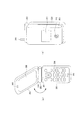
図3は本発明の第3実施形態としての無線通信装置であるクラムシェル型携帯電話機を表す図である。図3のクラムシェル型携帯電話機は、その回路方式において図1および図2を参照して既述の第1および第2の実施の形態としての無線通信装置の何れとも実質的に同様に構成され得るものであるが、その筐体部と実装に関して特徴を有する。
図3(a)はクラムシェル型携帯電話機を開いたときの状態を示す斜視図であり、図3(b)は、同クラムシェル型携帯電話機を閉じたときの状態を示す斜視図である。
FIG. 3 is a diagram showing a clamshell type mobile phone as a wireless communication apparatus as a third embodiment of the present invention. The clamshell mobile phone of FIG. 3 is configured in substantially the same manner as any of the wireless communication apparatuses as the first and second embodiments described above with reference to FIGS. 1 and 2 in the circuit system. Although it is to be obtained, it has features with respect to its housing and mounting.
FIG. 3A is a perspective view showing a state when the clamshell mobile phone is opened, and FIG. 3B is a perspective view showing a state when the clamshell mobile phone is closed.
図3(a)および図3(b)において、第1筐体部301の表面には、操作ボタン304が配置されると共に、第1筐体部301の下端にはマイク305が設けられ、第1筐体部301の上端には外部無線通信用アンテナ306が取り付けられている。また、第2筐体部302の表面(開いた状態で現れる面)には、表示部308が設けられるとともに、第2筐体部302の上端にはスピーカ309が設けられている。
また、第2筐体部302の裏面(閉じた状態での外面)には、表示体311および撮像素子312が設けられている。なお、上述の表示体308および311としては、例えば、液晶表示パネル、有機ELパネルまたはプラズマディスプレイパネルなどが適用される。また、撮像素子312としては、CCDまたはCMOSセンサなどが適用される。
3A and 3B, an
In addition, a
第1筐体部301および第2筐体部302には、第1筐体部301と第2筐体部302との間で内部無線通信を行う内部無線通信用アンテナ307および310がそれぞれ設けられている。図示のように、第1筐体部301および第2筐体部302は、結合機構部(連結部)としてのヒンジ303を介して連結され、第2筐体部302をヒンジ303を支点として回転させることにより、第2筐体部302を第1筐体部301上に折り畳むことができる。
The
上述のようにして、第2筐体部302を第1筐体部301上に閉じることにより、操作ボタン304を第2筐体部302にて保護することができ、携帯電話を持ち歩く時に操作ボタン304が誤って操作されることを防止することができる。また、第2筐体部302を第1筐体部301から開くことにより、表示体308を見ながら操作ボタン304を操作したり、スピーカ309およびマイク305を使いながら通話したり、操作ボタン304を操作しながら撮像を行ったりすることができる。
As described above, the
また、クラムシェル構造を用いることにより、第2筐体部302のほぼ一面全体に表示体308を配置することができ、携帯電話機としての携帯性を損なうことなく、表示体308のサイズを拡大させることを可能として、視認性を向上させることができる。
上述の構成において、この携帯電話機では、第1筐体部301に内部無線通信用アンテナ307を、および、第2筐体部302に内部無線通信用アンテナ310をそれぞれ設けることにより、これらの内部無線通信用アンテナ307および310を用いた内部無線通信にて第1筐体部301と第2筐体部302との間のデータ伝送を行うように構成されていることを特徴としている。
In addition, by using the clamshell structure, the
In the above-described configuration, in this mobile phone, the internal wireless communication antenna 307 is provided in the
そして、図3の携帯電話機において、第1筐体部301側には、図1又は図2における1次側モジュールM1が設けられ、第2筐体部302側には、図1又は図2における2次側モジュールM2が設けられている。
また、内部無線通信用アンテナ307が図1及び図2における内部無線通信用アンテナ14に相応し、内部無線通信用アンテナ310が図1及び図2における内部無線通信用アンテナ32に相応する。
In the mobile phone of FIG. 3, the primary module M1 in FIG. 1 or FIG. 2 is provided on the
The internal wireless communication antenna 307 corresponds to the internal
上述の構成により、例えば、外部無線通信用アンテナ306を介して第1筐体部301に取り込まれた画像データや音声データを、内部無線通信用アンテナ307および310を用いた内部無線通信によって第2筐体部302に送り、表示部308に画像を表示させたり、スピーカ309から音声を出力させたりすることができる。
また、撮像素子312によって撮像された撮像データを、内部無線通信用アンテナ307および310を用いた内部無線通信によって第2筐体部302から第1筐体部301に送り、外部無線通信用アンテナ306を介して外部に送出させることができる。
上述のように、第1筐体部301と第2筐体部302との間のデータ伝送を有線で行う必要がなくなり、多ピン化されたフレキシブル配線基板をヒンジ303に通す必要がなくなる。
With the above-described configuration, for example, image data and audio data captured by the
In addition, image data captured by the
As described above, it is not necessary to perform data transmission between the
さらに、1次側モジュールM1が設けられた第1筐体部301と2次側モジュールM2が設けられた第2筐体部302との間で無接点で電力を伝送することを可能としつつ、1次側モジュールM1および2次側モジュールM2において、同一の電力搬送波クロックを基準として搬送波を生成することができる。このため、第1筐体部301と第2筐体部302との間で電力を授受するための電線をヒンジ403に通すことなく電力を伝送することができるとともに、1次側モジュールM1と2次側モジュールM2との間で無線データ通信を行う場合においても、基準クロックを生成するための局部発振器や、1次側モジュールM1と2次側モジュールM2とで基準クロックの周波数ずれを調整するための自動周波数調整回路やA/D変換器が不要となり、回路規模の増大を抑制しつつ、高速なデータ通信を無線にて実現することが可能となる。
Furthermore, while enabling electric power to be transmitted in a contactless manner between the
なお、以上はクラムシェル型携帯電話機の実施形態について説明したが、上述のような無線通信の技術を、回転式携帯電話機やノート型パーソナルコンピュータなど、各種電子機器に適用することもできる。 Although the embodiments of the clamshell mobile phone have been described above, the wireless communication technology as described above can be applied to various electronic devices such as a rotary mobile phone and a notebook personal computer.
図4は、本発明の第4実施形態に係る無線通信装置が適用されるシステム構成を示す外観図である。
図4において、デジタルカメラ51には図1の2次側モジュールM2が搭載され、充電台52には図1の1次側モジュールM1が搭載されているものとする。そして、充電台52にはACアダプタ54を介して交流電源が供給されるとともに、充電台52は、USB規格などの有線ケーブル55を介してパーソナルコンピュータ53と接続されている。
そして、充電台52は、デジタルカメラ51に無接点電力伝送を通じて充電を行うとともに、デジタルカメラ51と無線データ通信を行うことができる。そして、充電台52は、デジタルカメラ51から取得したデータを、有線ケーブル55を介してパーソナルコンピュータ53へ転送することができる。
FIG. 4 is an external view showing a system configuration to which a wireless communication apparatus according to the fourth embodiment of the present invention is applied.
In FIG. 4, it is assumed that the secondary side module M2 of FIG. 1 is mounted on the
The charging
なお、充電台52とパーソナルコンピュータ53との接続は有線ケーブル55以外にも、無線接続を用いるようにしてもよい。また、図4の実施形態では、デジタルカメラ51を例にとって説明したが、携帯電話やビデオカメラなどに適用するようにしてもよい。
In addition, the connection between the charging
M1 1次側モジュール、M2 2次側モジュール、1、21 ベースバンド部、12、22 制御部、3、23 ROM、4、24 RAM、5 電力搬送波クロック生成部、6 昇圧回路、7a 1次側コイル、7b 2次側コイル、7c 3次側コイル、8 遅延調整部、9、29 PLL回路、10、17、30、37 ローパスフィルタ、11、16、31、36 混合器、12、34 スイッチ、13、33 バンドパスフィルタ、15、35 ローノイズアンプ、18、38 バッファ、14、32 内部無線通信用アンテナ、25a〜25d ダイオード、26 コンデンサ、27 電圧レギュレータ回路、28 降圧回路、51 デジタルカメラ、52 充電台、53 パーソナルコンピュータ、54 ACアダプタ、55 有線ケーブル M1 primary module, M2 secondary module, 1,21 baseband unit, 12, 22 control unit, 3, 23 ROM, 4, 24 RAM, 5 power carrier clock generation unit, 6 booster circuit, 7a primary side Coil, 7b secondary coil, 7c tertiary coil, 8 delay adjuster, 9, 29 PLL circuit, 10, 17, 30, 37 low pass filter, 11, 16, 31, 36 mixer, 12, 34 switch, 13, 33 Bandpass filter, 15, 35 Low noise amplifier, 18, 38 Buffer, 14, 32 Internal wireless communication antenna, 25a to 25d Diode, 26 Capacitor, 27 Voltage regulator circuit, 28 Step-down circuit, 51 Digital camera, 52 Charging Stand, 53 personal computer, 54 AC adapter, 55 wired cable
Claims (5)
前記無線送信部から無線送信された信号と前記搬送波と同じ周波数成分を有する搬送波とを混合して前記送信データの受信を行う無線受信部と、
前記無線送信部または前記無線受信部のいずれか一方にのみ設けられ、電力搬送波クロックを生成する電力搬送波クロック生成部と、
前記電力搬送波クロックによって起こる電磁誘導にて前記無線送信部と前記無線受信部との間で電力を伝送する無接点電力伝送手段と、
前記無線送信部または前記無線受信部のうちの前記電力搬送波クロック生成部が設けられた方に搭載され、前記電力搬送波クロックに基づいて搬送波を生成する搬送波生成手段と、
前記無線送信部または前記無線受信部のうちの前記電力搬送波クロック生成部が設けられていない方に搭載され、前記無接点電力伝送手段のうちの電力受信側で誘起された前記電力搬送波クロックと同じ周波数成分を有するクロックに基づいて、前記搬送波生成手段にて生成された搬送波と同じ周波数成分を有する搬送波を再生する搬送波再生手段とを備えることを特徴とする無線通信装置。 A wireless transmission unit that wirelessly transmits a signal by modulating a carrier wave with transmission data;
A wireless receiver that receives the transmission data by mixing a signal wirelessly transmitted from the wireless transmitter and a carrier having the same frequency component as the carrier;
A power carrier clock generator that is provided only in either the wireless transmitter or the wireless receiver and generates a power carrier clock;
Contactless power transmission means for transmitting power between the wireless transmitter and the wireless receiver by electromagnetic induction caused by the power carrier clock;
A carrier wave generating means mounted on the one of the radio transmitter and the radio receiver provided with the power carrier clock generator and generating a carrier wave based on the power carrier clock;
Same as the power carrier clock induced on the power reception side of the non-contact power transmission means mounted on the wireless transmission unit or the wireless reception unit not provided with the power carrier clock generation unit A radio communication apparatus comprising: carrier recovery means for recovering a carrier having the same frequency component as the carrier generated by the carrier generation means based on a clock having a frequency component.
を備えることを特徴とする請求項1に記載の無線通信装置。 The carrier recovery means is a step-down circuit for stepping down a voltage of a clock having the same frequency component as the power carrier clock induced on the power receiving side of the contactless power transmission means, and the step-down circuit steps down the voltage. A frequency multiplication means for multiplying the frequency of the generated clock;
The wireless communication apparatus according to claim 1, further comprising:
前記搬送波再生手段は、前記第2のコイルに電磁結合され、前記第2のコイルに誘起された前記電力搬送波クロックと同じ周波数成分を有するクロックにより前記電力搬送波クロックと同じ周波数成分を有するクロックが誘起される第3のコイルと、前記第3のコイルからの電力が供給され、前記第3のコイルに誘起されたクロックの周波数を逓倍する周波数逓倍手段と、を備えることを特徴とする請求項1に記載の無線通信装置。 The non-contact power transmission means includes a first coil on the power transmission side and a second coil on the power reception side,
The carrier recovery means is electromagnetically coupled to the second coil, and a clock having the same frequency component as the power carrier clock is induced by a clock having the same frequency component as that of the power carrier clock induced in the second coil. And a frequency multiplier for multiplying a frequency of a clock induced in the third coil by being supplied with electric power from the third coil. A wireless communication device according to 1.
前記1次側モジュールに搭載され、送信データにて搬送波を変調して信号の無線送信を行う無線送信部と、
前記2次側モジュールに搭載され、前記無線送信部から無線送信された信号と前記搬送波と同じ周波数成分を有する搬送波とを混合して前記送信データの受信を行う無線受信部と、
前記1次側モジュールまたは前記2次側モジュールのいずれか一方にのみ搭載され、電力搬送波クロックを生成する電力搬送波クロック生成部と、
前記電力搬送波クロックによって起こる電磁誘導にて前記1次側モジュールと前記2次側モジュールとの間で電力を伝送する無接点電力伝送手段と、
前記1次側モジュールと前記2次側モジュールのうちの前記電力搬送波クロック生成部が搭載された方に設けられ、前記電力搬送波クロックに基づいて搬送波を生成する搬送波生成手段と、
前記1次側モジュールと前記2次側モジュールのうちの前記電力搬送波クロック生成部が搭載されていない方に設けられ、前記無接点電力伝送手段のうちの電力受信側で誘起された前記電力搬送波クロックと同じ周波数成分を有するクロックに基づいて、前記搬送波生成手段にて生成された搬送波と同じ周波数成分を有する搬送波を再生する搬送波再生手段とを備えることを特徴とする無線通信装置。 A primary module and a secondary module that are separable from each other;
A wireless transmission unit mounted on the primary side module for performing wireless transmission of a signal by modulating a carrier wave with transmission data;
A radio receiver that is mounted on the secondary module and receives the transmission data by mixing a signal wirelessly transmitted from the radio transmitter and a carrier having the same frequency component as the carrier;
A power carrier clock generator that is mounted only on either the primary side module or the secondary side module and generates a power carrier clock;
Contactless power transmission means for transmitting power between the primary module and the secondary module by electromagnetic induction caused by the power carrier clock;
A carrier wave generating means provided on a side of the primary side module and the secondary side module on which the power carrier clock generator is mounted, and generating a carrier wave based on the power carrier clock;
The power carrier clock induced on the power reception side of the non-contact power transmission means provided on the primary module and the secondary module on which the power carrier clock generation unit is not mounted. And a carrier recovery means for recovering a carrier having the same frequency component as the carrier generated by the carrier generation means based on a clock having the same frequency component.
第2筐体部と、
前記第1筐体部と前記第2筐体部との間の位置関係を変えられるように前記第1筐体部と前記第2筐体部とを連結する連結部と、
前記第1筐体部に搭載され、外部無線通信を行う外部無線通信部と、
前記第2筐体部に搭載された表示部と、
前記第1筐体部に搭載され、送信データにて搬送波を変調して信号の内部無線送信を行う内部無線送信部と、
前記第2筐体部に搭載され、前記内部無線送信部から内部無線送信された信号と前記搬送波と同じ周波数成分を有する搬送波とを混合して前記送信データの内部無線受信を行う内部無線受信部と、
前記第1筐体部または前記第2筐体部のいずれか一方に搭載され、電力搬送波クロックを生成する電力搬送波クロック生成部と、
前記電力搬送波クロックによって起こる電磁誘導にて前記第1筐体部と前記第2筐体部との間で電力を伝送する無接点電力伝送手段と、
前記第1筐体部と前記第2筐体部のうちの前記電力搬送波クロック生成部が搭載された方に設けられ、前記電力搬送波クロックに基づいて搬送波を生成する搬送波生成手段と、 前記第1筐体部と前記第2筐体部のうちの前記電力搬送波クロック生成部が搭載されていない方に設けられ、前記無接点電力伝送手段のうちの電力受信側で誘起された前記電力搬送波クロックと同じ周波数成分を有するクロックに基づいて、前記搬送波生成手段にて生成された搬送波と同じ周波数成分を有する搬送波を再生する搬送波再生手段とを備えることを特徴とする無線通信装置。 A first housing part;
A second housing part;
A connecting portion that connects the first housing portion and the second housing portion so as to change a positional relationship between the first housing portion and the second housing portion;
An external wireless communication unit mounted on the first housing unit for performing external wireless communication;
A display unit mounted on the second housing unit;
An internal wireless transmission unit mounted on the first housing unit for performing internal wireless transmission of a signal by modulating a carrier wave with transmission data;
An internal radio receiving unit that is mounted on the second housing unit and that performs internal radio reception of the transmission data by mixing a signal that has been internally radio transmitted from the internal radio transmission unit and a carrier wave having the same frequency component as the carrier wave When,
A power carrier clock generator mounted on either the first housing part or the second housing part for generating a power carrier clock;
Contactless power transmission means for transmitting power between the first housing part and the second housing part by electromagnetic induction caused by the power carrier clock;
A carrier wave generating means provided on a side of the first casing part and the second casing part on which the power carrier clock generating part is mounted, and generating a carrier wave based on the power carrier clock; The power carrier clock that is provided on the side of the housing unit and the second housing unit on which the power carrier clock generation unit is not mounted, and is induced on the power reception side of the contactless power transmission means, and A radio communication apparatus comprising: a carrier reproduction unit that reproduces a carrier having the same frequency component as the carrier generated by the carrier generation unit based on a clock having the same frequency component.
Priority Applications (2)
| Application Number | Priority Date | Filing Date | Title |
|---|---|---|---|
| JP2006226007A JP2007143116A (en) | 2005-10-19 | 2006-08-23 | Wireless communication device |
| US11/550,608 US7627288B2 (en) | 2005-10-19 | 2006-10-18 | Wireless communication apparatus |
Applications Claiming Priority (2)
| Application Number | Priority Date | Filing Date | Title |
|---|---|---|---|
| JP2005304314 | 2005-10-19 | ||
| JP2006226007A JP2007143116A (en) | 2005-10-19 | 2006-08-23 | Wireless communication device |
Publications (1)
| Publication Number | Publication Date |
|---|---|
| JP2007143116A true JP2007143116A (en) | 2007-06-07 |
Family
ID=38205364
Family Applications (1)
| Application Number | Title | Priority Date | Filing Date |
|---|---|---|---|
| JP2006226007A Withdrawn JP2007143116A (en) | 2005-10-19 | 2006-08-23 | Wireless communication device |
Country Status (2)
| Country | Link |
|---|---|
| US (1) | US7627288B2 (en) |
| JP (1) | JP2007143116A (en) |
Cited By (8)
| Publication number | Priority date | Publication date | Assignee | Title |
|---|---|---|---|---|
| JP2008022045A (en) * | 2006-07-10 | 2008-01-31 | Ricoh Co Ltd | Receiver, transmitter and data communication system |
| JP2010028898A (en) * | 2008-07-15 | 2010-02-04 | Seiko Epson Corp | Power reception control device, power receiving device and electronic apparatus |
| WO2011105553A1 (en) | 2010-02-25 | 2011-09-01 | オリンパス株式会社 | Portable wireless terminal, wireless terminal device, and wireless communication system |
| JP2012105478A (en) * | 2010-11-11 | 2012-05-31 | Sony Corp | Transmission device, electronic equipment, and transmission method |
| JP2012105477A (en) * | 2010-11-11 | 2012-05-31 | Sony Corp | Transmission device, electronic equipment, and transmission method |
| JP2013232988A (en) * | 2013-08-08 | 2013-11-14 | Canon Inc | Communication device, control method therefor and program |
| JP2015089035A (en) * | 2013-10-31 | 2015-05-07 | 株式会社半導体理工学研究センター | Communication circuit |
| CN106329735A (en) * | 2016-11-24 | 2017-01-11 | 中核(天津)科技发展有限公司 | Non-contact power supply and data transmission device |
Families Citing this family (17)
| Publication number | Priority date | Publication date | Assignee | Title |
|---|---|---|---|---|
| US7937120B2 (en) * | 2007-04-21 | 2011-05-03 | Paratek Microwave, Inc. | System, apparatus and method for frequency based current reduction in wireless portable devices |
| JP4462341B2 (en) | 2007-12-18 | 2010-05-12 | ソニー株式会社 | Information processing apparatus and method, and program |
| JP5198475B2 (en) * | 2008-01-30 | 2013-05-15 | 京セラ株式会社 | Device with built-in data communication function |
| JP5159396B2 (en) * | 2008-04-03 | 2013-03-06 | キヤノン株式会社 | Communication device, control method thereof, and program |
| DE102008024217B4 (en) * | 2008-05-19 | 2016-04-14 | Airbus Operations Gmbh | System for contactless data and energy transmission and use of such a system in an aircraft |
| DE102009019994B4 (en) * | 2008-05-19 | 2020-08-13 | Airbus Operations Gmbh | Airplane with hybrid transmitters for contactless energy and data transmission |
| US8024012B2 (en) * | 2008-06-11 | 2011-09-20 | International Business Machines Corporation | Intelligent wireless power charging system |
| GB2464945B (en) * | 2008-10-29 | 2013-07-10 | Wfs Technologies Ltd | Electrical connector system |
| DE102009053584A1 (en) | 2009-11-17 | 2011-05-19 | Airbus Operations Gmbh | Carrier system for receiving containers in a vehicle and use of a carrier system in an aircraft |
| EP2515314B1 (en) * | 2009-12-17 | 2019-05-15 | Toyota Jidosha Kabushiki Kaisha | Non-contact power reception device and corresponding transmission device |
| GB2483374A (en) * | 2010-09-03 | 2012-03-07 | Wfs Technologies Ltd | Transferring power between a fixed unit and a rotating unit using a rotary transformer, and also transferring data |
| US9264108B2 (en) | 2011-10-21 | 2016-02-16 | Qualcomm Incorporated | Wireless power carrier-synchronous communication |
| CN203233187U (en) * | 2013-01-08 | 2013-10-09 | 光碁科技股份有限公司 | Waterproof zero-connecting hole portable electronic product |
| EP3566320B1 (en) * | 2017-01-04 | 2023-07-12 | Koninklijke Philips N.V. | Device for wireless transmission of data and/or power |
| US10432249B1 (en) * | 2018-06-14 | 2019-10-01 | The Boeing Company | Universal nonlinear variable delay filter |
| CN112814841A (en) * | 2020-12-31 | 2021-05-18 | 天津瑞源电气有限公司 | Remote communication and maintenance system of pitch control system based on power line carrier |
| CN116707166A (en) * | 2022-02-25 | 2023-09-05 | 华为技术有限公司 | Wireless power supply and communication method and cradle head camera |
Family Cites Families (9)
| Publication number | Priority date | Publication date | Assignee | Title |
|---|---|---|---|---|
| JP3344593B2 (en) | 1992-10-13 | 2002-11-11 | 株式会社ソニー木原研究所 | Wireless power supply |
| US5649295A (en) * | 1995-06-19 | 1997-07-15 | Lucent Technologies Inc. | Dual mode modulated backscatter system |
| JPH09103037A (en) | 1995-10-05 | 1997-04-15 | Nippon Ido Tsushin Kk | Power supply unit, unit to be supplied with power and power supply system |
| US5940447A (en) * | 1996-08-30 | 1999-08-17 | Motorola, Inc. | Wireless powered communication device using power signal sampling and method |
| JP3916291B2 (en) * | 1997-03-28 | 2007-05-16 | ローム株式会社 | Information communication equipment |
| TW463399B (en) * | 1999-03-19 | 2001-11-11 | Seiko Epson Corp | Electronic device |
| FR2808942B1 (en) * | 2000-05-12 | 2002-08-16 | St Microelectronics Sa | VALIDATION OF THE PRESENCE OF AN ELECTROMAGNETIC TRANSPONDER IN THE FIELD OF A PHASE DEMODULATION READER |
| US7072697B2 (en) * | 2002-10-22 | 2006-07-04 | Nokia Corporation | Method and device for transponder aided wake-up of a low power radio device by a wake-up event |
| JP2005073350A (en) | 2003-08-22 | 2005-03-17 | Matsushita Electric Works Ltd | Power tool |
-
2006
- 2006-08-23 JP JP2006226007A patent/JP2007143116A/en not_active Withdrawn
- 2006-10-18 US US11/550,608 patent/US7627288B2/en not_active Expired - Fee Related
Cited By (9)
| Publication number | Priority date | Publication date | Assignee | Title |
|---|---|---|---|---|
| JP2008022045A (en) * | 2006-07-10 | 2008-01-31 | Ricoh Co Ltd | Receiver, transmitter and data communication system |
| JP2010028898A (en) * | 2008-07-15 | 2010-02-04 | Seiko Epson Corp | Power reception control device, power receiving device and electronic apparatus |
| WO2011105553A1 (en) | 2010-02-25 | 2011-09-01 | オリンパス株式会社 | Portable wireless terminal, wireless terminal device, and wireless communication system |
| JP2011176972A (en) * | 2010-02-25 | 2011-09-08 | Olympus Corp | Portable wireless terminal, wireless terminal device, and wireless communication system |
| JP2012105478A (en) * | 2010-11-11 | 2012-05-31 | Sony Corp | Transmission device, electronic equipment, and transmission method |
| JP2012105477A (en) * | 2010-11-11 | 2012-05-31 | Sony Corp | Transmission device, electronic equipment, and transmission method |
| JP2013232988A (en) * | 2013-08-08 | 2013-11-14 | Canon Inc | Communication device, control method therefor and program |
| JP2015089035A (en) * | 2013-10-31 | 2015-05-07 | 株式会社半導体理工学研究センター | Communication circuit |
| CN106329735A (en) * | 2016-11-24 | 2017-01-11 | 中核(天津)科技发展有限公司 | Non-contact power supply and data transmission device |
Also Published As
| Publication number | Publication date |
|---|---|
| US7627288B2 (en) | 2009-12-01 |
| US20070254726A1 (en) | 2007-11-01 |
Similar Documents
| Publication | Publication Date | Title |
|---|---|---|
| JP2007143116A (en) | Wireless communication device | |
| WO2019192600A1 (en) | Method and apparatus for screen projection of data, storage medium and electronic device | |
| JP3642332B2 (en) | Folding mobile phone device | |
| EP2495842B1 (en) | Non-contact power transmission apparatus | |
| JP4742841B2 (en) | Wireless communication device | |
| JP2006180453A (en) | Radio communications terminal and radio communication control method | |
| US7706494B2 (en) | Wireless communication apparatus | |
| JP2005217909A (en) | Electronic equipment and diversity antenna control method | |
| JP2007134896A (en) | Mobile terminal device and information transmitting method | |
| CN107026314A (en) | The antenna of mobile terminal | |
| CN106909072A (en) | Intelligent watch | |
| JP4082417B2 (en) | Electronic device, wireless communication terminal, and data transmission method | |
| JP2006270308A (en) | Camera module | |
| EP2257043A1 (en) | Portable television reception device | |
| CN210075302U (en) | Electronic device | |
| JP4293071B2 (en) | Wireless communication terminal | |
| TW201338331A (en) | Mobile device and method for controlling mobile device | |
| JP4218609B2 (en) | Wireless communication terminal and internal wireless communication control method | |
| CN210093260U (en) | Electronic device | |
| JP4710989B2 (en) | Wireless communication terminal and wireless communication control method | |
| KR100595618B1 (en) | Mobile communication terminal with dual camera | |
| JP3493290B2 (en) | Power supply control device in portable information communication terminal | |
| KR100698548B1 (en) | Mobile phone including slot | |
| CN118050811A (en) | Communication method, electronic device, and storage medium | |
| JP4424251B2 (en) | Wireless communication terminal |
Legal Events
| Date | Code | Title | Description |
|---|---|---|---|
| A621 | Written request for application examination |
Free format text: JAPANESE INTERMEDIATE CODE: A621 Effective date: 20090708 |
|
| A977 | Report on retrieval |
Free format text: JAPANESE INTERMEDIATE CODE: A971007 Effective date: 20101220 |
|
| A761 | Written withdrawal of application |
Free format text: JAPANESE INTERMEDIATE CODE: A761 Effective date: 20110121 |