JP2007133351A - Display unit, active matrix device, and driving method thereof - Google Patents
Display unit, active matrix device, and driving method thereof Download PDFInfo
- Publication number
- JP2007133351A JP2007133351A JP2006097995A JP2006097995A JP2007133351A JP 2007133351 A JP2007133351 A JP 2007133351A JP 2006097995 A JP2006097995 A JP 2006097995A JP 2006097995 A JP2006097995 A JP 2006097995A JP 2007133351 A JP2007133351 A JP 2007133351A
- Authority
- JP
- Japan
- Prior art keywords
- circuit
- column
- data
- row
- output
- Prior art date
- Legal status (The legal status is an assumption and is not a legal conclusion. Google has not performed a legal analysis and makes no representation as to the accuracy of the status listed.)
- Pending
Links
Images


Classifications
-
- G—PHYSICS
- G09—EDUCATION; CRYPTOGRAPHY; DISPLAY; ADVERTISING; SEALS
- G09G—ARRANGEMENTS OR CIRCUITS FOR CONTROL OF INDICATING DEVICES USING STATIC MEANS TO PRESENT VARIABLE INFORMATION
- G09G3/00—Control arrangements or circuits, of interest only in connection with visual indicators other than cathode-ray tubes
- G09G3/20—Control arrangements or circuits, of interest only in connection with visual indicators other than cathode-ray tubes for presentation of an assembly of a number of characters, e.g. a page, by composing the assembly by combination of individual elements arranged in a matrix no fixed position being assigned to or needed to be assigned to the individual characters or partial characters
- G09G3/22—Control arrangements or circuits, of interest only in connection with visual indicators other than cathode-ray tubes for presentation of an assembly of a number of characters, e.g. a page, by composing the assembly by combination of individual elements arranged in a matrix no fixed position being assigned to or needed to be assigned to the individual characters or partial characters using controlled light sources
- G09G3/30—Control arrangements or circuits, of interest only in connection with visual indicators other than cathode-ray tubes for presentation of an assembly of a number of characters, e.g. a page, by composing the assembly by combination of individual elements arranged in a matrix no fixed position being assigned to or needed to be assigned to the individual characters or partial characters using controlled light sources using electroluminescent panels
- G09G3/32—Control arrangements or circuits, of interest only in connection with visual indicators other than cathode-ray tubes for presentation of an assembly of a number of characters, e.g. a page, by composing the assembly by combination of individual elements arranged in a matrix no fixed position being assigned to or needed to be assigned to the individual characters or partial characters using controlled light sources using electroluminescent panels semiconductive, e.g. using light-emitting diodes [LED]
- G09G3/3208—Control arrangements or circuits, of interest only in connection with visual indicators other than cathode-ray tubes for presentation of an assembly of a number of characters, e.g. a page, by composing the assembly by combination of individual elements arranged in a matrix no fixed position being assigned to or needed to be assigned to the individual characters or partial characters using controlled light sources using electroluminescent panels semiconductive, e.g. using light-emitting diodes [LED] organic, e.g. using organic light-emitting diodes [OLED]
- G09G3/3225—Control arrangements or circuits, of interest only in connection with visual indicators other than cathode-ray tubes for presentation of an assembly of a number of characters, e.g. a page, by composing the assembly by combination of individual elements arranged in a matrix no fixed position being assigned to or needed to be assigned to the individual characters or partial characters using controlled light sources using electroluminescent panels semiconductive, e.g. using light-emitting diodes [LED] organic, e.g. using organic light-emitting diodes [OLED] using an active matrix
- G09G3/3233—Control arrangements or circuits, of interest only in connection with visual indicators other than cathode-ray tubes for presentation of an assembly of a number of characters, e.g. a page, by composing the assembly by combination of individual elements arranged in a matrix no fixed position being assigned to or needed to be assigned to the individual characters or partial characters using controlled light sources using electroluminescent panels semiconductive, e.g. using light-emitting diodes [LED] organic, e.g. using organic light-emitting diodes [OLED] using an active matrix with pixel circuitry controlling the current through the light-emitting element
-
- G—PHYSICS
- G09—EDUCATION; CRYPTOGRAPHY; DISPLAY; ADVERTISING; SEALS
- G09G—ARRANGEMENTS OR CIRCUITS FOR CONTROL OF INDICATING DEVICES USING STATIC MEANS TO PRESENT VARIABLE INFORMATION
- G09G3/00—Control arrangements or circuits, of interest only in connection with visual indicators other than cathode-ray tubes
- G09G3/20—Control arrangements or circuits, of interest only in connection with visual indicators other than cathode-ray tubes for presentation of an assembly of a number of characters, e.g. a page, by composing the assembly by combination of individual elements arranged in a matrix no fixed position being assigned to or needed to be assigned to the individual characters or partial characters
- G09G3/22—Control arrangements or circuits, of interest only in connection with visual indicators other than cathode-ray tubes for presentation of an assembly of a number of characters, e.g. a page, by composing the assembly by combination of individual elements arranged in a matrix no fixed position being assigned to or needed to be assigned to the individual characters or partial characters using controlled light sources
- G09G3/30—Control arrangements or circuits, of interest only in connection with visual indicators other than cathode-ray tubes for presentation of an assembly of a number of characters, e.g. a page, by composing the assembly by combination of individual elements arranged in a matrix no fixed position being assigned to or needed to be assigned to the individual characters or partial characters using controlled light sources using electroluminescent panels
- G09G3/32—Control arrangements or circuits, of interest only in connection with visual indicators other than cathode-ray tubes for presentation of an assembly of a number of characters, e.g. a page, by composing the assembly by combination of individual elements arranged in a matrix no fixed position being assigned to or needed to be assigned to the individual characters or partial characters using controlled light sources using electroluminescent panels semiconductive, e.g. using light-emitting diodes [LED]
- G09G3/3208—Control arrangements or circuits, of interest only in connection with visual indicators other than cathode-ray tubes for presentation of an assembly of a number of characters, e.g. a page, by composing the assembly by combination of individual elements arranged in a matrix no fixed position being assigned to or needed to be assigned to the individual characters or partial characters using controlled light sources using electroluminescent panels semiconductive, e.g. using light-emitting diodes [LED] organic, e.g. using organic light-emitting diodes [OLED]
- G09G3/3275—Details of drivers for data electrodes
- G09G3/3283—Details of drivers for data electrodes in which the data driver supplies a variable data current for setting the current through, or the voltage across, the light-emitting elements
-
- G—PHYSICS
- G09—EDUCATION; CRYPTOGRAPHY; DISPLAY; ADVERTISING; SEALS
- G09G—ARRANGEMENTS OR CIRCUITS FOR CONTROL OF INDICATING DEVICES USING STATIC MEANS TO PRESENT VARIABLE INFORMATION
- G09G2300/00—Aspects of the constitution of display devices
- G09G2300/08—Active matrix structure, i.e. with use of active elements, inclusive of non-linear two terminal elements, in the pixels together with light emitting or modulating elements
- G09G2300/0809—Several active elements per pixel in active matrix panels
- G09G2300/0842—Several active elements per pixel in active matrix panels forming a memory circuit, e.g. a dynamic memory with one capacitor
- G09G2300/0861—Several active elements per pixel in active matrix panels forming a memory circuit, e.g. a dynamic memory with one capacitor with additional control of the display period without amending the charge stored in a pixel memory, e.g. by means of additional select electrodes
-
- G—PHYSICS
- G09—EDUCATION; CRYPTOGRAPHY; DISPLAY; ADVERTISING; SEALS
- G09G—ARRANGEMENTS OR CIRCUITS FOR CONTROL OF INDICATING DEVICES USING STATIC MEANS TO PRESENT VARIABLE INFORMATION
- G09G2310/00—Command of the display device
- G09G2310/02—Addressing, scanning or driving the display screen or processing steps related thereto
- G09G2310/0202—Addressing of scan or signal lines
- G09G2310/0218—Addressing of scan or signal lines with collection of electrodes in groups for n-dimensional addressing
-
- G—PHYSICS
- G09—EDUCATION; CRYPTOGRAPHY; DISPLAY; ADVERTISING; SEALS
- G09G—ARRANGEMENTS OR CIRCUITS FOR CONTROL OF INDICATING DEVICES USING STATIC MEANS TO PRESENT VARIABLE INFORMATION
- G09G2310/00—Command of the display device
- G09G2310/02—Addressing, scanning or driving the display screen or processing steps related thereto
- G09G2310/0262—The addressing of the pixel, in a display other than an active matrix LCD, involving the control of two or more scan electrodes or two or more data electrodes, e.g. pixel voltage dependent on signals of two data electrodes
-
- G—PHYSICS
- G09—EDUCATION; CRYPTOGRAPHY; DISPLAY; ADVERTISING; SEALS
- G09G—ARRANGEMENTS OR CIRCUITS FOR CONTROL OF INDICATING DEVICES USING STATIC MEANS TO PRESENT VARIABLE INFORMATION
- G09G2310/00—Command of the display device
- G09G2310/02—Addressing, scanning or driving the display screen or processing steps related thereto
- G09G2310/0264—Details of driving circuits
- G09G2310/027—Details of drivers for data electrodes, the drivers handling digital grey scale data, e.g. use of D/A converters
-
- G—PHYSICS
- G09—EDUCATION; CRYPTOGRAPHY; DISPLAY; ADVERTISING; SEALS
- G09G—ARRANGEMENTS OR CIRCUITS FOR CONTROL OF INDICATING DEVICES USING STATIC MEANS TO PRESENT VARIABLE INFORMATION
- G09G2310/00—Command of the display device
- G09G2310/02—Addressing, scanning or driving the display screen or processing steps related thereto
- G09G2310/0264—Details of driving circuits
- G09G2310/0272—Details of drivers for data electrodes, the drivers communicating data to the pixels by means of a current
-
- G—PHYSICS
- G09—EDUCATION; CRYPTOGRAPHY; DISPLAY; ADVERTISING; SEALS
- G09G—ARRANGEMENTS OR CIRCUITS FOR CONTROL OF INDICATING DEVICES USING STATIC MEANS TO PRESENT VARIABLE INFORMATION
- G09G2310/00—Command of the display device
- G09G2310/02—Addressing, scanning or driving the display screen or processing steps related thereto
- G09G2310/0264—Details of driving circuits
- G09G2310/0297—Special arrangements with multiplexing or demultiplexing of display data in the drivers for data electrodes, in a pre-processing circuitry delivering display data to said drivers or in the matrix panel, e.g. multiplexing plural data signals to one D/A converter or demultiplexing the D/A converter output to multiple columns
-
- G—PHYSICS
- G09—EDUCATION; CRYPTOGRAPHY; DISPLAY; ADVERTISING; SEALS
- G09G—ARRANGEMENTS OR CIRCUITS FOR CONTROL OF INDICATING DEVICES USING STATIC MEANS TO PRESENT VARIABLE INFORMATION
- G09G2320/00—Control of display operating conditions
- G09G2320/02—Improving the quality of display appearance
- G09G2320/0233—Improving the luminance or brightness uniformity across the screen
-
- G—PHYSICS
- G09—EDUCATION; CRYPTOGRAPHY; DISPLAY; ADVERTISING; SEALS
- G09G—ARRANGEMENTS OR CIRCUITS FOR CONTROL OF INDICATING DEVICES USING STATIC MEANS TO PRESENT VARIABLE INFORMATION
- G09G2320/00—Control of display operating conditions
- G09G2320/02—Improving the quality of display appearance
- G09G2320/029—Improving the quality of display appearance by monitoring one or more pixels in the display panel, e.g. by monitoring a fixed reference pixel
- G09G2320/0295—Improving the quality of display appearance by monitoring one or more pixels in the display panel, e.g. by monitoring a fixed reference pixel by monitoring each display pixel
-
- G—PHYSICS
- G09—EDUCATION; CRYPTOGRAPHY; DISPLAY; ADVERTISING; SEALS
- G09G—ARRANGEMENTS OR CIRCUITS FOR CONTROL OF INDICATING DEVICES USING STATIC MEANS TO PRESENT VARIABLE INFORMATION
- G09G2320/00—Control of display operating conditions
- G09G2320/04—Maintaining the quality of display appearance
- G09G2320/043—Preventing or counteracting the effects of ageing
-
- G—PHYSICS
- G09—EDUCATION; CRYPTOGRAPHY; DISPLAY; ADVERTISING; SEALS
- G09G—ARRANGEMENTS OR CIRCUITS FOR CONTROL OF INDICATING DEVICES USING STATIC MEANS TO PRESENT VARIABLE INFORMATION
- G09G2330/00—Aspects of power supply; Aspects of display protection and defect management
- G09G2330/02—Details of power systems and of start or stop of display operation
-
- G—PHYSICS
- G09—EDUCATION; CRYPTOGRAPHY; DISPLAY; ADVERTISING; SEALS
- G09G—ARRANGEMENTS OR CIRCUITS FOR CONTROL OF INDICATING DEVICES USING STATIC MEANS TO PRESENT VARIABLE INFORMATION
- G09G3/00—Control arrangements or circuits, of interest only in connection with visual indicators other than cathode-ray tubes
- G09G3/20—Control arrangements or circuits, of interest only in connection with visual indicators other than cathode-ray tubes for presentation of an assembly of a number of characters, e.g. a page, by composing the assembly by combination of individual elements arranged in a matrix no fixed position being assigned to or needed to be assigned to the individual characters or partial characters
- G09G3/2092—Details of a display terminals using a flat panel, the details relating to the control arrangement of the display terminal and to the interfaces thereto
- G09G3/2096—Details of the interface to the display terminal specific for a flat panel
Abstract
Description
本発明は、電気光学素子又は画素回路をマトリクス状に配置した表示装置及びアクティブマトリクス装置と、それらの駆動方法に関する。 The present invention relates to a display device and an active matrix device in which electro-optical elements or pixel circuits are arranged in a matrix, and driving methods thereof.
近年、次世代ディスプレイとして電気光学素子を用いたディスプレイ等が注目されている。ここでは、素子に流れる電流によって発光輝度が制御される電流制御型の発光素子である有機エレクトロルミネッセンス(EL)素子を例に挙げて説明する。 In recent years, a display using an electro-optical element has attracted attention as a next-generation display. Here, an organic electroluminescence (EL) element, which is a current-controlled light-emitting element whose emission luminance is controlled by a current flowing through the element, will be described as an example.
周辺回路を含んだ有機ELディスプレイでは、表示領域に限らず、周辺回路においても薄膜トランジスタ(TFT)が用いられている。このような自発光素子であるEL素子を画像表示素子に利用し、その表示領域および周辺回路にTFTを用いた画像表示パネルについて、以下、図面を参照して説明する。 In an organic EL display including a peripheral circuit, a thin film transistor (TFT) is used not only in the display area but also in the peripheral circuit. An image display panel using such an EL element, which is a self-luminous element, as an image display element and using TFTs in its display region and peripheral circuit will be described below with reference to the drawings.
図16に示すELパネル100には、RGB原色数のEL素子と、このEL素子に入力される電流を制御するためのTFTから構成される画素(画素回路)2とがN列×M行の2次元状に配列された画素表示部9と、その周辺回路とが配置される。周辺回路のうち、入力回路6には、外部より水平走査制御信号11aが入力される。また、入力回路7には、外部より垂直走査制御信号12aが入力される。さらに、入力回路8には、外部より補助列制御信号13aが入力される。
The
入力回路6にて変換された水平走査制御信号11(水平クロック信号と水平走査開始信号)は、列シフトレジスタ3に入力される。また、入力回路7にて変換された垂直走査制御信号12は、行シフトレジスタ5に入力される。行シフトレジスタ5の各出力端子から出力された行走査信号は、行選択線20としての走査線を介して各行の画素回路2に入力される。
The horizontal scanning control signal 11 (horizontal clock signal and horizontal scanning start signal) converted by the
また、入力回路8にて変換された補助列制御信号13は、ゲート回路4、16にそれぞれ入力される。水平シフトレジスタ3の各端子から出力される水平サンプリング信号17は、ゲート回路16にて変換された制御信号21と共に、水平サンプリング信号ゲート回路15に入力される。水平サンプリング信号ゲート回路15にて変換される水平サンプリング信号18は、外部より入力された映像信号(電圧信号)10と、ゲート回路4にて変換された制御信号19と共に、列駆動回路1に入力される。列駆動回路1にて映像信号から変換された電流信号である列制御信号14は、データ線を介して各列の画素回路2に入力される。
The auxiliary
列駆動回路1は、画素回路2の各列の原色数(例えば、赤、緑、青の3色)に応じて複数配置され、各原色数の入力映像信号10に対応するように構成される。この列駆動回路1は、1画素毎の時系列に入力される点順次電圧映像信号を行単位で同時に出力可能な線順次電流映像信号に変換する電圧電流変換回路を用いている。
A plurality of
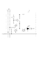
図17は、列駆動回路1に用いられる電圧電流変換回路の構成例である。
FIG. 17 is a configuration example of a voltage-current conversion circuit used in the
図17において、gmは電圧電流変換回路、M0乃至M3はpチャンネル型TFT、M4乃至M6はnチャンネル型TFT、V(data)は電圧電流変換回路gmに入力される映像信号電圧、I(data)は電圧電流変換回路gmからデータ線に出力される電流信号(データ信号)、VCCは電源、V0は基準電流バイアス値、Vrefは基準電圧、P0は制御信号である。M2とM3はソース結合回路、M4とM5はカレントミラー回路を構成する。 In FIG. 17, gm is a voltage-current conversion circuit, M0 to M3 are p-channel TFTs, M4 to M6 are n-channel TFTs, V (data) is a video signal voltage input to the voltage-current conversion circuit gm, I (data ) Is a current signal (data signal) output from the voltage-current conversion circuit gm to the data line, VCC is a power supply, V0 is a reference current bias value, Vref is a reference voltage, and P0 is a control signal. M2 and M3 constitute a source coupling circuit, and M4 and M5 constitute a current mirror circuit.
図17に示す電圧電流変換回路gmにおいて、映像信号電圧V(data)がTFT(M2)のゲートGに入力される。すると、TFT(M1)のドレイン電流を基準電流として、ソース結合回路、カレントミラー回路を介して、映像信号電圧V(data)の電圧値に応じた電流値をもつ電流信号I(data)が生成され、データ線に出力される。 In the voltage-current conversion circuit gm shown in FIG. 17, the video signal voltage V (data) is input to the gate G of the TFT (M2). Then, using the drain current of the TFT (M1) as a reference current, a current signal I (data) having a current value corresponding to the voltage value of the video signal voltage V (data) is generated via the source coupling circuit and the current mirror circuit. And output to the data line.
この回路では、電圧電流変換ゲインは、M0とM1、M2とM3、M4とM5の各々で互いに相関性がある場合、M1のドレイン電流と、M2、M3の駆動能力によって決定される。なお、列駆動回路1の他の回路構成や駆動方法は、特許文献1に記載の図1、図2に示されている。
In this circuit, the voltage-current conversion gain is determined by the drain current of M1 and the drive capacities of M2 and M3 when M0 and M1, M2 and M3, and M4 and M5 are correlated with each other. Other circuit configurations and driving methods of the
しかしながら、上記TFTは、非単結晶半導体を活性層に用いているため、その特性上、単結晶を活性層に用いたトランジスタに比べて素子間のばらつきが大きく、近接的にもばらつきに相関性が保証できない。TFTの閾値やキャリア移動度等のばらつきにより、列駆動回路の電圧電流変換ゲインが素子間で異なると、EL素子に供給される電流値が画素間でばらつく。そうすると、EL素子が所望の輝度で発光することができない。その結果、表示領域において輝度のばらつきとなって表れる。 However, since the TFT uses a non-single crystal semiconductor for the active layer, the characteristics of the TFT are larger than those of a transistor using a single crystal for the active layer. Cannot be guaranteed. If the voltage / current conversion gain of the column drive circuit differs between elements due to variations in TFT thresholds, carrier mobility, etc., the current value supplied to the EL element varies between pixels. Then, the EL element cannot emit light with a desired luminance. As a result, luminance variations appear in the display area.
そのため、特許文献2には、輝度ばらつきを抑制するための回路構成が記載されている。この回路構成によれば、画素回路を駆動する列駆動回路の出力電流を検出して基準電流データと比較して補正係数を演算し、その補正係数を用いて列駆動回路へ入力される映像信号を補正して輝度ばらつきを軽減している。
しかしながら、特許文献2に記載されているような、列駆動回路の出力電流を検出して補正をする方法では、画素密度が増え、列駆動回路の出力が小さくなる場合には、充分なSN比をもつ検出信号が得られないことがある。また、列駆動回路の数が増えるにつれて、検出に費やす時間及び補正処理に費やす時間が無視できなくなる。
However, in the method of detecting and correcting the output current of the column driving circuit as described in
また、特許文献1に記載されているような、従来の表示装置においては、1つの列駆動回路の電流出力先は、1フレーム走査期間中常に同じデータ線である。つまり、1つの列駆動回路の電流出力先は、1フレーム走査期間中常に同じ列の画素回路2に入力される。
In the conventional display device as described in
従って、電気光学素子や画素回路にばらつきが全く無いものと仮定した場合、全画素に同じ輝度レベルの1フレームの表示画像信号を入力し、これを表示したときに、列毎に輝度がばらつくことがある。 Therefore, when it is assumed that there is no variation in the electro-optical element and the pixel circuit, when one frame of display image signal having the same luminance level is input to all the pixels and displayed, the luminance varies from column to column. There is.
本発明は、複数列のEL素子などの電気光学素子に流れる電流のばらつきを時間的に平均化することで、輝度ばらつきを低減させる表示装置およびその駆動方法を提供することを目的とする。 An object of the present invention is to provide a display device and a driving method thereof that reduce luminance variations by temporally averaging variations in currents flowing through electro-optical elements such as a plurality of columns of EL elements.
上記目的を達成するため、本発明に係る表示装置は、複数の電気光学素子を有する画素がマトリクス状に配置された表示部と、
前記表示部の行毎に共通に接続された複数の行選択線と、
前記表示部に列毎に共通に接続された複数のデータ線と、
前記表示部の列に対応して設けられ、入力される映像信号を前記画素に供給されるデータ信号に変換して前記複数のデータ線に行毎に同時に出力する複数の列駆動回路と、
を有する表示装置において、
前記列駆動回路の出力先となるデータ線を選択するための選択回路と、
前記列駆動回路の出力先となるデータ線を一垂直走査期間より短い単位水平走査期間毎に順次変更するように、前記選択回路を制御する制御回路と、
を有することを特徴とする。
In order to achieve the above object, a display device according to the present invention includes a display unit in which pixels having a plurality of electro-optic elements are arranged in a matrix,
A plurality of row selection lines connected in common to each row of the display unit;
A plurality of data lines commonly connected to the display section for each column;
A plurality of column driving circuits which are provided corresponding to the columns of the display unit, convert input video signals into data signals supplied to the pixels, and simultaneously output the data signals to the plurality of data lines for each row;
In a display device having
A selection circuit for selecting a data line as an output destination of the column drive circuit;
A control circuit for controlling the selection circuit so as to sequentially change the data line as the output destination of the column driving circuit for each unit horizontal scanning period shorter than one vertical scanning period;
It is characterized by having.
本発明に係わるアクティブマトリクス装置は、複数の画素回路がマトリクス状に配置されたマトリクス回路部と、
前記マトリクス回路部の行毎に共通に接続された複数の行選択線と、
前記マトリクス回路部に列毎に共通に接続された複数のデータ線と、
前記マトリクス回路部の列に対応して設けられ、入力される映像信号を前記画素回路に供給されるデータ信号に変換して前記複数のデータ線に行毎に同時に出力する複数の列駆動回路と、
を有するアクティブマトリクス装置において、
前記列駆動回路の出力先となるデータ線を選択するための選択回路と、
前記列駆動回路の出力先となるデータ線を一垂直走査期間より短い単位水平走査期間毎に順次変更するように、前記選択回路を制御する制御回路と、
を有することを特徴とする。
An active matrix device according to the present invention includes a matrix circuit unit in which a plurality of pixel circuits are arranged in a matrix,
A plurality of row selection lines connected in common to each row of the matrix circuit portion;
A plurality of data lines commonly connected to the matrix circuit portion for each column;
A plurality of column driving circuits which are provided corresponding to the columns of the matrix circuit unit, convert input video signals into data signals supplied to the pixel circuits, and simultaneously output the data signals to the plurality of data lines for each row; ,
In an active matrix device having:
A selection circuit for selecting a data line as an output destination of the column drive circuit;
A control circuit for controlling the selection circuit so as to sequentially change a data line as an output destination of the column driving circuit for each unit horizontal scanning period shorter than one vertical scanning period;
It is characterized by having.
本発明において、前記画素回路は、前記映像信号の表示色を決める3つの原色画素に対応して配置され、前記複数のデータ線は、前記3つの原色画素に対応する列に配置される3つのデータ線を有し、前記複数の列駆動回路は、3つの列駆動回路であり、前記選択手段は、前記3つの原色画素のうち任意の原色画素に対応する列に配置されたデータ線に対して前記3つの列駆動回路のうち1つの列駆動回路からのデータ信号を出力可能に選択する手段であってもよい。 In the present invention, the pixel circuit is arranged corresponding to three primary color pixels that determine a display color of the video signal, and the plurality of data lines are arranged in three columns corresponding to the three primary color pixels. And the plurality of column drive circuits are three column drive circuits, and the selecting unit applies data lines arranged in columns corresponding to arbitrary primary color pixels among the three primary color pixels. Further, a means for selecting a data signal from one column driving circuit out of the three column driving circuits may be used.
本発明において、前記複数の列駆動回路の総和出力電流を検出し、検出された前記総和出力電流に基づいて前記列駆動回路に入力される映像信号を列毎に補正する補正手段をさらに有してもよい。前記電流制御型表示素子は、エレクトロルミネセンス素子であってもよい。 In the present invention, there is further provided correction means for detecting a total output current of the plurality of column drive circuits and correcting a video signal input to the column drive circuit for each column based on the detected total output current. May be. The current control type display element may be an electroluminescence element.
本発明においては、共通のデータ線に接続された隣接行の画素回路には、1フレーム走査期間内に同じ列駆動回路からの出力が供給されないように、インターレース走査により行を選択することも好ましいものである。 In the present invention, it is also preferable to select a row by interlaced scanning so that the output from the same column driving circuit is not supplied to the pixel circuits in adjacent rows connected to the common data line within one frame scanning period. Is.
また、本発明においては、3単位水平ライン周期で、少なくとも3つの前記列駆動回路の前記データ信号出力先が3色のデータ線となるように、前記選択手段を制御することも好ましいものである。 In the present invention, it is also preferable to control the selection means so that the data signal output destinations of at least three of the column drive circuits are three color data lines in a unit horizontal line period. .
本発明に係る表示装置及びアクティブマトリクス装置の駆動方法は、
前記列駆動回路の出力先となるデータ線を選択する工程と、
前記列駆動回路のデータ信号出力先となるデータ線を一垂直走査期間より短い単位水平ライン周期で順次変更する工程と、
を含むことを特徴とする。
A display device and a driving method of an active matrix device according to the present invention include:
Selecting a data line as an output destination of the column drive circuit;
Sequentially changing a data line to which a data signal is output from the column driving circuit in a unit horizontal line period shorter than one vertical scanning period;
It is characterized by including.
本発明によれば、列駆動回路の出力先のデータ線を順次変更しながら、その出力を画素或いは画素回路に供給するように構成する。こうして、画素或いは画素回路に供給される電流の値のばらつきを時間的に平均化、換言すれば空間的に分散させることができる。よって、画面に現れる縦筋のような、表示画像の不均一性を視覚的に低減できる。 According to the present invention, the output destination data line of the column driving circuit is sequentially changed, and the output is supplied to the pixel or the pixel circuit. In this way, variations in the value of the current supplied to the pixel or pixel circuit can be averaged over time, in other words, spatially dispersed. Therefore, it is possible to visually reduce display image non-uniformity such as vertical stripes appearing on the screen.
以下、本発明に係る表示装置或いはアクティブマトリクス装置を実施するための最良の形態について、図面を参照して具体的に説明する。 Hereinafter, the best mode for carrying out a display device or an active matrix device according to the present invention will be specifically described with reference to the drawings.
本発明に用いられる電気光学素子としては、有機EL素子、無機EL素子、電子放出素子を用いた発光素子、発光ダイオードなどが挙げられる。 Examples of the electro-optical element used in the present invention include an organic EL element, an inorganic EL element, a light-emitting element using an electron-emitting element, and a light-emitting diode.
画素は、上記電気光学素子からなるパッシブマトリクス回路であってもよく、或いは、画素は、少なくとも1つのトランジスタを有するアクティブマトリクス回路を構成していてもよい。 The pixel may be a passive matrix circuit composed of the electro-optic element, or the pixel may constitute an active matrix circuit having at least one transistor.
本発明に用いられる列駆動回路は、映像信号をデータ信号に変換する回路が好ましく用いられる。映像信号としては、アナログ電圧信号、デジタル信号などが好適に用いられる。データ信号としては、画素の輝度を決定するためのアナログ電流信号が好ましく用いられる。 As the column driving circuit used in the present invention, a circuit for converting a video signal into a data signal is preferably used. As the video signal, an analog voltage signal, a digital signal, or the like is preferably used. As the data signal, an analog current signal for determining the luminance of the pixel is preferably used.
そして、列駆動回路は、パッシブマトリクス回路を構成する電気光学素子に供給されるデータ信号を供給する回路、或いは、アクティブマトリクス回路を構成する画素回路に供給されるデータ信号を供給する回路となる。 The column drive circuit is a circuit that supplies a data signal supplied to the electro-optic element that constitutes the passive matrix circuit, or a circuit that supplies a data signal supplied to the pixel circuit that constitutes the active matrix circuit.
列駆動回路を構成する電圧電流変換回路は、一列に1個設けられる場合以外に、一列に2個づつ設けられ、1水平走査期間毎に切り替えて用いられてもよい。或いは、4つの列駆動回路を3列のデータ線毎に設け、そのうち、2つの列駆動回路を一つのデータ線に接続する構成であってもよい。 In addition to the case where one voltage-current conversion circuit constituting the column driving circuit is provided in one row, two voltage-current conversion circuits may be provided in one row and may be used by switching every horizontal scanning period. Alternatively, four column driving circuits may be provided for every three data lines, and two column driving circuits may be connected to one data line.
本発明は、列駆動回路を構成するトランジスタに製造プロセスに起因する特性ばらつきが生じやすい回路に有効に働くため、非単結晶半導体を活性層に用いたTFTにて構成された列駆動回路に好適に用いられる。非単結晶半導体とは非晶質シリコン、多結晶シリコン、微結晶シリコンである。或いは、単結晶シリコンのような単結晶半導体を活性層に用いたトランジスタであっても、特性ばらつきが無視し得ない回路であれば、本発明が適用可能である。 The present invention is effective for a circuit in which characteristic variation due to a manufacturing process easily occurs in a transistor constituting a column driving circuit, and is therefore suitable for a column driving circuit including a TFT using a non-single crystal semiconductor as an active layer. Used for. The non-single-crystal semiconductor is amorphous silicon, polycrystalline silicon, or microcrystalline silicon. Alternatively, the present invention can be applied to a transistor in which a single crystal semiconductor such as single crystal silicon is used for an active layer as long as the characteristic variation cannot be ignored.
本発明のデータ信号は、マトリクス回路の画素又は画素回路のうち同じ行選択線により選択可能な同一行の画素又は画素回路に同時に供給される。この行選択期間は水平走査期間に相当し、全ての行を順次選択することで1フレーム走査期間におけるデータ信号の出力が完了する。 The data signal of the present invention is simultaneously supplied to pixels or pixel circuits in the same row that can be selected by the same row selection line among the pixels or pixel circuits of the matrix circuit. This row selection period corresponds to a horizontal scanning period, and the output of data signals in one frame scanning period is completed by sequentially selecting all the rows.
本発明においては、列駆動回路の出力先となるデータ線を単位水平走査期間毎に順次変更する。ここで単位水平走査期間とは1水平走査期間或いは2乃至3水平走査期間ように、所定の水平走査期間であればよいが、好ましくは1水平走査期間であることが望まれる。 In the present invention, the data line as the output destination of the column drive circuit is sequentially changed every unit horizontal scanning period. Here, the unit horizontal scanning period may be a predetermined horizontal scanning period such as one horizontal scanning period or two to three horizontal scanning periods, but it is desirable that the unit horizontal scanning period is one horizontal scanning period.
本発明は、電気光学素子を用いたマトリクス型表示装置に適用されているが、EL素子のような電気光学素子を形成する前のアクティブマトリクス装置にも好ましく用いられる。 The present invention is applied to a matrix display device using an electro-optical element, but is preferably used also for an active matrix device before forming an electro-optical element such as an EL element.
本実施形態に係る表示装置は、電気光学素子およびTFTを含む画素回路がマトリクス状に配置された表示部(アクティブマトリクス部)を有する。そして、データ線にデータ信号を出力するデータ線駆動回路と、行選択線(走査線)に走査信号を出力する走査線駆動回路とを有する。また、映像信号や制御信号の入力、および電源供給を行う端子部と、各画素の電気光学素子と接続された共通配線と、を有する。共通配線は、表示領域の周辺を囲んで配置されており、配線引出部から配線を引いて端子部の一部と接続される。 The display device according to the present embodiment includes a display unit (active matrix unit) in which pixel circuits including electro-optic elements and TFTs are arranged in a matrix. The data line driving circuit outputs a data signal to the data line, and the scanning line driving circuit outputs a scanning signal to the row selection line (scanning line). In addition, a terminal portion that inputs video signals and control signals and supplies power, and a common wiring connected to the electro-optical element of each pixel are provided. The common wiring is arranged so as to surround the periphery of the display area, and is connected to a part of the terminal portion by drawing the wiring from the wiring lead portion.
本発明においては、必要に応じて、複数の列駆動回路の出力電流を検出し、それを評価して、当該複数の列駆動回路へ入力される映像信号を補正する補正回路を有することも好ましいものである。 In the present invention, it is also preferable to have a correction circuit that detects output currents of a plurality of column drive circuits, evaluates them, and corrects video signals input to the plurality of column drive circuits as necessary. Is.
また、本発明においては、列駆動回路の出力先が単位水平走査期間毎に変更されるため、列駆動回路に入力される映像信号は、その変更を考慮してサンプリングされるか、映像信号の供給順序を列単位で並び替える必要がある。具体的には、列駆動回路への入力サンプリングを制御するか、映像信号を供給する回路(補正回路)側で供給順序を列単位で並び替える制御を行えばよい。 In the present invention, since the output destination of the column driving circuit is changed every unit horizontal scanning period, the video signal input to the column driving circuit is sampled in consideration of the change, or the video signal It is necessary to rearrange the supply order in units of columns. Specifically, input sampling to the column drive circuit may be controlled, or control for rearranging the supply order in units of columns may be performed on the circuit (correction circuit) side that supplies the video signal.
本実施形態によれば、列駆動回路の出力先のデータ線を順次変更し、電気光学素子に供給される電流の値のばらつきを時間的に平均化する。換言すれば、空間的にばらつきを分散することで、表示画像の不均一性を視覚的に低減できる。 According to this embodiment, the data lines of the output destination of the column drive circuit are sequentially changed, and the variation in the value of the current supplied to the electro-optical element is averaged over time. In other words, the non-uniformity of the display image can be visually reduced by spatially dispersing the variation.
そして、列駆動回路の出力先のデータ線を変更する周期を一垂直走査期間より短い単位水平走査期間毎とする。垂直走査期間とは一フィールド走査期間または一フレーム走査期間である。即ち単位水平ライン周期とすることで、単位フレーム周期と比較して、出力先のデータ線を変更する周期が短いため、視覚的な画素間ばらつきをさらに低減できる。 Then, the cycle of changing the output destination data line of the column driving circuit is set to be a unit horizontal scanning period shorter than one vertical scanning period. The vertical scanning period is one field scanning period or one frame scanning period. In other words, by setting the unit horizontal line period, the period of changing the output data line is shorter than the unit frame period, so that the visual inter-pixel variation can be further reduced.
(第1の実施形態)
図1は、第1の実施形態による表示装置の構成を示す模式図である。
(First embodiment)
FIG. 1 is a schematic diagram illustrating a configuration of a display device according to the first embodiment.
なお、前述した図16に示す従来例と同様の構成要素については、同一符号を付している。また、図16で記載した入力回路6、7、8については省略している。
It should be noted that the same components as those in the conventional example shown in FIG. Also, the
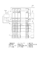
図1に示す表示装置は、表示パネル100を有する。表示パネル100の共通基板には、RGB原色数のEL素子と、このEL素子に入力される電流を制御するためのTFTから構成される画素回路2とがN列×M行の2次元状に配列された画像表示部9と、周辺回路とが配置される。周辺回路には、前述した図16に示す従来例と同様の列駆動回路1、列シフトレジスタ3、行シフトレジスタ5、ゲート回路4を備える。その他、本実施形態では、列駆動回路1と画素回路2の間に、列駆動回路1より出力された電流信号を総和電流として出力する総和電流出力回路29と、本発明の主要部を構成する選択回路34とを備える。総和電流出力回路1の制御信号入力側には、ゲート回路30が接続される。総和電流出力回路1の出力側には、総和電流を検出する総和電流検出回路33が接続される。総和電流検出回路33の出力側には、検出された総和電流が入力される補正回路32が接続される。映像信号電圧Videoは、補正回路32を介して列駆動回路1に入力される。
The display device illustrated in FIG. 1 includes a
上記構成のうち、選択回路34及び制御回路35以外の回路、即ち列駆動回路1、画素回路2、総和電流出力回路29、補正回路32については、前述した特許文献1、2等の先行技術文献に開示されている回路構成を適用可能である。
Among the above-described configurations, circuits other than the
まず、前述した列駆動回路以外の各回路の構成および動作について順次説明する。 First, the configuration and operation of each circuit other than the column drive circuit described above will be sequentially described.
(総和電流出力回路)
図2は、本実施例の総和電流出力回路29の回路構成例を示す。
(Total current output circuit)
FIG. 2 shows a circuit configuration example of the total
図中、43は列駆動回路1の出力が共通に接続される電流信号出力線、41は列駆動回路1の出力と電流信号出力線43との接続関係を制御するスイッチ部、42は列駆動回路1と画素側との接続関係を制御するスイッチ部である遮断部、data1a乃至dataNcはデータ線、M11乃至M3N、M41乃至M6NはスイッチとしてのTFT、Ioutは総和電流、CCx,CCyは総和電流検出用制御信号である。
In the figure, 43 is a current signal output line to which the output of the
総和電流出力回路29より総和電流を出力して映像信号の補正を行うには、通常の動作期間の前に補正期間を設ける。この補正期間において、総和電流出力回路29のスイッチ部41のM11乃至M3NをCCxにより全てオンにし、遮断部42のM41乃至M6NをCCyにより全てオフとする。以上の動作により、列駆動回路1から出力された電流信号は、画素回路2には流れず、全て出力線43より出力される。
To correct the video signal by outputting the total current from the total
そして、R、G、Bの3列のスイッチM11、M21、M31に対応する列駆動回路に検出用の所定の明レベルの入力電圧を与え、他の全列の列駆動回路には例えば最大暗レベルの入力電圧を与える。すると、3列のスイッチM11、M21、M31に対応する列駆動回路から加算された検出電流信号が得られ、これが基準データと比較され、スイッチM11、M21、M31に対応する列駆動回路一組の補正係数k1が算出される。 Then, an input voltage of a predetermined light level for detection is applied to the column drive circuits corresponding to the switches M11, M21, and M31 of the three columns R, G, and B, and the maximum darkness is applied to the column drive circuits of all the other columns. Give level input voltage. Then, a detection current signal added from the column drive circuit corresponding to the three columns of switches M11, M21, and M31 is obtained, and this is compared with the reference data, and a set of column drive circuits corresponding to the switches M11, M21, and M31 is set. A correction coefficient k1 is calculated.
続いて、R、G、Bの3列のスイッチM12、M22、M32に対応する列駆動回路に検出用の所定の明レベルの入力電圧を与え、他の全列の列駆動回路には例えば最大暗レベルの入力電圧を与える。すると、スイッチM12、M22、M32に対応する列駆動回路の3列から加算された検出電流信号が得られ、これが基準データと比較され、スイッチM12、M22、M32に対応した列駆動回路一組の補正係数k2が算出される。この動作を時系列的に順次、水平方向に選択される列駆動回路一組を変更しながら、補正係数k1、k2・・・kNを算出する。このように、一つの列駆動回路から順次検出信号を得るのではなく、所定個数(ここでは3つ)の列駆動回路をまとめて、それらの加算値として検出信号を得ている。よって、検出時間は3分の1に短縮され、また、所望のSN比の検出信号を得ることができる。 Subsequently, an input voltage having a predetermined light level for detection is applied to the column drive circuits corresponding to the switches M12, M22, and M32 in the three columns R, G, and B, and the maximum value is applied to the column drive circuits of all the other columns. Provides dark level input voltage. Then, a detection current signal added from the three columns of the column drive circuit corresponding to the switches M12, M22, and M32 is obtained, and this is compared with the reference data, and a set of column drive circuits corresponding to the switches M12, M22, and M32 is set. A correction coefficient k2 is calculated. The correction coefficients k1, k2,... KN are calculated while changing the set of column drive circuits selected in the horizontal direction sequentially in time series. In this way, instead of sequentially obtaining detection signals from one column driving circuit, a predetermined number (three in this case) of column driving circuits are collected and a detection signal is obtained as an added value thereof. Therefore, the detection time is shortened to one third, and a detection signal having a desired S / N ratio can be obtained.
また、補正回路32において補正に必要な演算時間も3分の1に短縮されるので、映像信号の高速処理が可能となる。
In addition, since the calculation time required for correction in the
ここで、一つの列駆動回路としては、特許文献1の図1の回路を採用することも好ましいものである。この場合、補正のための検出時には、一対の電圧電流変換回路に同じ検出用の所定の明レベルの入力電圧を与え、これら一対の電圧電流変換回路からの出力電流を加算して同時に検出するようにしている。このように、本実施形態によれば、6つ(2×RGB)の電圧電流変換回路から同時に検出信号を加算して得てもよい。 Here, as one column drive circuit, it is also preferable to employ the circuit of FIG. In this case, at the time of detection for correction, an input voltage of the same predetermined light level for detection is applied to the pair of voltage / current conversion circuits, and the output currents from the pair of voltage / current conversion circuits are added and detected simultaneously. I have to. Thus, according to the present embodiment, the detection signals may be simultaneously added from six (2 × RGB) voltage-current conversion circuits.
なお、図2中、スイッチを構成するトランジスタをNチャネル型としたが、それに限らない。 In FIG. 2, the transistor constituting the switch is an N-channel type, but the present invention is not limited to this.
(補正回路)
本実施形態の補正回路32は、R、G、B3本のデータ線からなる組毎に検出された電流信号と、基準となる電流信号とで演算処理を行い、補正係数k1乃至kNを得て、その補正係数k1乃至kNを記憶する。R、G、Bの3つの入力信号Videoが補正回路32に記憶された共通の補正係数k1乃至kNを用いて補正される。こうして補正された映像信号がR、G、Bの3つの列駆動回路1に順次入力される。列駆動回路1の出力電流は、データ線を介して画素回路2に入力される。ここで、隣接する3つの列駆動回路1に入力されるR、G、Bの信号は総和電流により得られた補正係数で補正されているため、各列駆動回路毎の近接的なばらつき、例えば隣合う列のEL素子に流れ込む電流に関しては不十分である。本実施形態は、その対策として、後述する選択回路34を用いるものである、という見方もできる。
(Correction circuit)
The
RGB各色画素毎の画素データをシリアルに転送する構成の補正回路を採用する場合には、上述したように、列駆動回路の出力先の変更に併せて、RGB各色画素データの出力順序を変更した映像信号を供給することもできる。 When employing a correction circuit configured to serially transfer pixel data for each RGB color pixel, as described above, the output order of the RGB color pixel data was changed in accordance with the change of the output destination of the column drive circuit. A video signal can also be supplied.
(画素回路)
図3は、本実施例のEL素子を含む画素回路2の構成例を示す。
(Pixel circuit)
FIG. 3 shows a configuration example of the
図3において、P1及びP2が行選択線20に印加される走査信号であり、データ信号として電流データIdataが入力される。EL素子の陽極(アノード)はTFT(M4)のドレイン端子に接続されており、陰極(カソード)は接地電位CGNDに接続されている。M1、M2、M4がP型TFTであり、M3がN型TFTである。
In FIG. 3, P1 and P2 are scanning signals applied to the
図4は、画素回路2の駆動方法を説明するタイミングチャートである。図4において、I(m−1)、I(m)、I(m+1)は、m−1行(1行前)、m行(対象行)、m+1行(1行後)の対象列の画素回路2に入力される電流データIdataを示す。
FIG. 4 is a timing chart illustrating a method for driving the
まず、時刻t0前の時点では、対象行の画素回路2には、走査信号P1にはLowレベルの信号が、P2にはHighレベルの信号が入力され、トランジスタM2がOFF、M3がOFF、M4がONの状態である。この状態では、対象行であるm行の画素回路2には、1行前の電流データIdataに対応するI(m−1)は入力されない。
First, at a time point before time t0, a low level signal is input to the
次いで、時刻t0では、P1にはHighレベルの信号が、P2にはLowレベルの信号が入力され、トランジスタM2、M3がON、M4はOFFとなる。この状態で、m行の画素回路2に該当行の電流データIdataに対応するI(m)が入力される。このとき、M4は導通状態でないため、EL素子には電流が流れない。入力されたIdataによりM1の電流駆動能力に応じた電圧が、M1のゲート端子と電源電位VCCの間に配置された容量C1に生じる。つまり、画素回路で一旦
電流電圧変換を行う。
Next, at time t0, a high level signal is input to P1, a low level signal is input to P2, and the transistors M2 and M3 are turned on and M4 is turned off. In this state, I (m) corresponding to the current data Idata of the corresponding row is input to the
次いで、時刻t1では、P2にHighレベルの信号が入力され、M2がOFFの状態となる。さらに、時刻t2では、P1にLowレベルの信号が入力され、M3がOFF、M4がONとなる。この状態では、M4が導通状態であるため、C1に生じた電圧により、M1の電流駆動能力に応じた電流がEL素子に供給される。つまり、ここで再び電流に変換される。これにより、供給された電流に応じた輝度でEL素子が発光する。 Next, at time t1, a high-level signal is input to P2, and M2 is turned off. Further, at time t2, a low level signal is input to P1, M3 is OFF, and M4 is ON. In this state, since M4 is in a conductive state, a current corresponding to the current driving capability of M1 is supplied to the EL element by the voltage generated in C1. In other words, it is converted again into current here. As a result, the EL element emits light with a luminance corresponding to the supplied current.
本実施例においては画素回路として、図3の構成を一例に挙げたが、これに限るものではない。 In the present embodiment, the configuration of FIG. 3 is given as an example of the pixel circuit, but is not limited thereto.
(選択回路)
次に、本実施例の選択回路34について、図5および図6を参照して説明する。ここでは、R(赤)、G(緑)、B(青)に割当てた画素回路で構成された画素を例にして説明する。
(Selection circuit)
Next, the
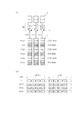
図5は、R、G、Bそれぞれの列と1対1に対応した列駆動回路1と、総和電流出力回路29の概略図である。図中の例では、R1、G1、B1は1列目の画素に、またR2、G2、B2は2列目の画素に、さらにR3、G3、B3は3列目の画素に、以下同様にRn、Gn、Bnはn列目の画素にそれぞれ対応する列駆動回路1を示す。
FIG. 5 is a schematic diagram of the
前述の補正回路により得られた補正係数k1乃至kNで補正をかけた出力電流のばらつきをさらに低減させるために、本実施形態では、列駆動回路1と画素回路2の間に選択回路34を備え、この選択回路34により列駆動回路1とデータ線14を単位水平走査期間毎に順次切り替える制御を行う。
In this embodiment, a
例えば、上記の手段のように列駆動回路1の総和出力電流を用いて3列の列駆動回路1の補正係数k1を得た場合、3列の列駆動回路1それぞれの出力とそれに対応する3つのデータ線の接続関係を順次切り替える。これにより、画素回路2には時間的に平均化された電流が入力されるようになる。
For example, when the correction coefficient k1 of the three
以上の構成を持つことにより、画素間でのばらつきと近接的なばらつきを低減させることが可能である。なお、データ線の切り替えを3列の列駆動回路1で説明したが、本発明はそれに限らない。
By having the above configuration, it is possible to reduce variations between pixels and close variations. Although the switching of the data lines has been described with the three
図6は、列電流を時間的に平均化する選択回路34の概略図である。図6では、不図示であるが、列駆動回路1と選択回路34との間に、前述した総和電流出力回路29が必要に応じて設けられている。
FIG. 6 is a schematic diagram of a
図6において、R、G、Bは各色に対応する入力映像信号Video、Gm1乃至Gm3は1列の画素を構成するR、G、Bの画素回路に対応する3列の列駆動回路1を示す。M11乃至M13、M21乃至M23、M31乃至M33は、Gm1、Gm2、Gm3の出力側の接続されるスイッチとしてのトランジスタを示す。
In FIG. 6, R, G, and B are input video signals Video, Gm1 to Gm3 corresponding to the respective colors, and three columns of
L1は、M11、M21、M31のゲート端子に、L2はM12、M22、M32のゲート端子に、L3はM13、M23、M33のゲート端子にそれぞれ接続されるON/OFF制御用の制御信号を示す。14r、14g、14bは、1列の画素を構成するR、G、Bの各画素回路に接続されるR列、G列、B列の各データ線14のそれぞれに接続される共通線を示す。なお、L1乃至L3の制御信号は、選択回路34の外部(又は内部)に設けた制御回路としてのゲート回路(ロジック回路)35から、予め設定された動作タイミングで出力されるようになっている。
L1 is a control signal for ON / OFF control connected to the gate terminals of M11, M21, and M31, L2 is connected to the gate terminals of M12, M22, and M32, and L3 is connected to the gate terminals of M13, M23, and M33. .
つまり、制御信号L1乃至L3を出力する回路は、単結晶半導体を用いた集積回路で表示パネルの外部に設けられた回路、或いは、非単結晶半導体を用いて、表示パネルと同じ基板上にTFTで形成された薄膜半導体集積回路であってもよい。 That is, a circuit that outputs the control signals L1 to L3 is an integrated circuit using a single crystal semiconductor and is provided on the same substrate as the display panel using a circuit provided outside the display panel or a non-single crystal semiconductor. The thin film semiconductor integrated circuit formed in (1) may be used.
図6において、Gm1、Gm2、Gm3の各入力端には、R、G、B各色の映像信号の配線に個別に接続されている。そして、列駆動回路の出力先の変更に応じて、各列駆動回路がサンプリングする映像信号の種類(色)も変更される。 In FIG. 6, the input terminals of Gm1, Gm2, and Gm3 are individually connected to the wiring of video signals of R, G, and B colors. Then, according to the change of the output destination of the column driving circuit, the type (color) of the video signal sampled by each column driving circuit is also changed.
Gm1の出力端には、スイッチM11、M12、M13及びそれらの接続配線と、共通線14r、14g、14bを介して、R、G、B各色のデータ線14が接続されている。Gm2の出力端には、スイッチM21、M22、M23及びそれらの接続配線と、共通線14r、14g、14bを介して、R、G、B各色のデータ線14が接続されている。Gm3の出力端には、スイッチM31、M32、M33とそれらの接続配線と、共通線14r、14g、14bを介して、R、G、B各色のデータ線14が接続されている。
The
上記構成により、選択回路34内のトランジスタのスイッチON/OFF制御により、例えば、Gm1の出力先のデータ線14をR列→G列→B列、G列→B列→R列、B列→R列→G列のように、単位水平走査期間毎に切り替えることが可能である。
With the above configuration, for example, the
次に、図7および図8を参照して、選択回路34の動作を説明する。
Next, the operation of the
図7は制御回路35の出力タイミングチャート、図8はその駆動シーケンスを示す。図7のタイミングチャートは、選択回路34のトランジスタで構成されたスイッチのゲート端子に入力されるL1乃至L3の信号の電位を示す。また、T1乃至T4は、予め設定された単位水平走査期間(単位水平ライン周期)を示す。図8において、No.は駆動シーケンス番号、ON_SWはON状態のトランジスタ、OFF_SWはOFF状態のトランジスタを示す。I(gm1)、I(gm2)、I(gm3)はそれぞれGm1、Gm2、Gm3の電流信号を示す。
FIG. 7 shows an output timing chart of the
図7において、まず、第1の単位水平ライン周期T1では、L1のみにHighレベルの信号が入力され、L2およびL3にはLowレベルの信号が入力される。このとき、選択回路34のM11、M21、M31のトランジスタのみがONとなり、その他のトランジスタはOFFである。この状態では、Gm1はBの電流信号I(gm1)を、Gm2はRの電流信号I(gm2)を、Gm3はGの電流信号I(gm3)を、それぞれ共通線14b、14r、14gを介して、B列、G列、B列の各データ線14に出力する。この周期T1は、図8に示す駆動シーケンスNo.1に対応する。
In FIG. 7, first, in the first unit horizontal line cycle T1, a high level signal is input only to L1, and a low level signal is input to L2 and L3. At this time, only the transistors M11, M21, and M31 of the
次いで、第2の単位水平ライン周期T2では、L2のみにHighレベルが入力され、L1およびL3はLOWレベルの信号が入力される。このとき選択回路34のM12、M22、M32のトランジスタがONとなり、その他のトランジスタはOFFである。この状態では、Gm1はGの電流信号I(gm1)を、Gm2はBの電流信号I(gm2)を、Gm3はRの電流信号I(gm3)を、それぞれ共通線14g、14b、14rを介して、G列、B列、R列の各データ線14に出力する。この周期T2は、図8に示す駆動シーケンスNo.2に対応する。
Next, in the second unit horizontal line cycle T2, a high level is input only to L2, and a low level signal is input to L1 and L3. At this time, the transistors M12, M22, and M32 of the
次いで、第3の単位水平ライン周期T3では、L3のみHighレベルが入力され、L1およびL2はLowレベルの信号が入力される。このとき選択回路34のM13、M23、M33のトランジスタがONとなり、その他のトランジスタはOFFである。この状態では、Gm1はRの電流信号I(gm1)を、Gm2はGの電流信号I(gm2)を、Gm3はBの電流信号I(gm3)を、それぞれ共通線14r、14g、14bを介して、R列、G列、B列の各データ線14に出力する。この周期T3は、図8に示す駆動シーケンスNo.3に対応する。
Next, in the third unit horizontal line cycle T3, a high level is input only to L3, and a low level signal is input to L1 and L2. At this time, the transistors M13, M23, and M33 of the
次いで、第4の周期T4では、第1の周期T1と同様の動作が行われ、これ以降、上記と同様の動作が繰り返し実行される。 Next, in the fourth cycle T4, the same operation as that in the first cycle T1 is performed, and thereafter, the same operation as described above is repeatedly executed.
以上のように選択回路34と制御回路35により、列駆動回路1の出力先を順次変更する。
As described above, the output destination of the
なお、説明の中で図6中の選択回路34のトランジスタをNチャネル型としたがそれに限らない。また、画素構成をRGBの3色一組としたがそれに限らない。従って、本実施形態によれば、TFT等の絶縁ゲート型電界効果トランジスタの素子特性ばらつきによるEL素子に流れる電流ばらつきを大幅に低減できる。加えて、近接する列毎の特性ばらつきを時間的に平均化することで、表示装置の視覚的なムラやスジ等といった課題を軽減することが出来る。
In the description, the transistor of the
(実施形態2)
本実施形態は、2つのフィールド(EVEN/ODDフィールドとする)からなるインターレース走査方式で表示を行う表示装置の例である。
(Embodiment 2)
The present embodiment is an example of a display device that performs display by an interlaced scanning method including two fields (EVEN / ODD fields).
図9は、6行3列の画素回路のマトリクスに0行から5行まで順次行を選択しながらノンインターレース走査を行う場合を示している。 FIG. 9 shows a case where non-interlaced scanning is performed while sequentially selecting 0 to 5 rows in a 6 × 3 pixel circuit matrix.
この場合、選択回路34によって、データ線Data1に接続される列駆動回路1の順序は、Gm1、Gm2、Gm3、Gm1、Gm2、Gm3の順となる。
In this case, the order of the
しかしながら、このように動作する選択回路34を用いて、インターレース走査を行う場合には、改善すべき課題がある。
However, when interlace scanning is performed using the
図10に示すように、EVEN/ODDフィールドで同じ分散順序(列駆動回路とデータ線の接続順序)では、隣接する2行(EVEN/ODD)の画素には同じ列駆動回路から電流データ信号が供給されることになる。すると、分散周期が長くなり分散周期が視認されやすくなる。 As shown in FIG. 10, in the same distribution order (column drive circuit and data line connection order) in the EVEN / ODD field, adjacent two rows (EVEN / ODD) of pixels receive current data signals from the same column drive circuit. Will be supplied. Then, the dispersion cycle becomes long and the dispersion cycle becomes easy to be visually recognized.
そこで、本実施形態では、偶数行を表示する第1のフィールドと奇数行を表示する第2のフィールドによって1フレームを表示するインターレース走査方式で表示を行う。そして、列駆動回路の出力先となるデータ線を単位水平走査期間毎に順次変更しながら、選択されたデータ線を介して列駆動回路からのデータ信号を画素回路に供給し、第1のフィールドと第2のフィールドではデータ線を順次選択する順序を異ならしめる。 Therefore, in the present embodiment, display is performed by an interlace scanning method in which one frame is displayed by a first field that displays even-numbered rows and a second field that displays odd-numbered rows. Then, the data signal from the column driving circuit is supplied to the pixel circuit via the selected data line while sequentially changing the data line as the output destination of the column driving circuit for each unit horizontal scanning period, and the first field is supplied. In the second field, the order in which the data lines are sequentially selected is made different.
本実施形態における表示装置の駆動方法について図11を用いて説明する。簡略化のため表示画素を6行×3列の18画素とする。Gm1乃至Gm3は列駆動回路を示し、映像信号電圧に応じた電流データ信号を出力する。34は選択回路であり、列駆動回路の出力先となるデータ線を選択する。Psは選択回路34を制御する選択制御信号であり、制御回路35から出力される。
A method of driving the display device in this embodiment will be described with reference to FIG. For simplification, display pixels are 18 pixels of 6 rows × 3 columns. Reference numerals Gm1 to Gm3 denote column driving circuits, which output current data signals corresponding to the video signal voltage.
選択信号Psによりスイッチの接点を単位走査期間毎に切り替え、列駆動回路を順次変更しながら、データ線を介して列駆動回路からの電流データ信号を同じ列の画素回路に供給する。 The contact point of the switch is switched for each unit scanning period by the selection signal Ps, and the current data signal from the column driving circuit is supplied to the pixel circuit of the same column through the data line while sequentially changing the column driving circuit.
図11において選択回路34の接点(1、2、3)を選択する順序は、EVENフィールドにおいては1→3→2→1→・・・、ODDフィールドにおいては2→1→3→2→・・・としている。ただし、選択する順序はこの限りではない。各画素に記載されたGm1乃至Gm3は該画素に電流データ信号を供給する列駆動回路を示している。このように各列の画素には、行毎に3つの列駆動回路を切り替え、かつフィールド毎に変更順序を変えて電流データ信号が供給される。
In FIG. 11, the selection order of the contacts (1, 2, 3) of the
また、この分散表示において前記複数のデータ線を選択するときに、3つの原色画素のうち任意の原色画素に対応する列に配置されたデータ線に対して3つの列駆動回路のうち1つの列駆動回路からの電流データ信号を出力可能に選択することが好ましい。 In addition, when the plurality of data lines are selected in the distributed display, one column of the three column driving circuits is used for the data line arranged in the column corresponding to an arbitrary primary color pixel among the three primary color pixels. It is preferable to select the current data signal from the drive circuit so that it can be output.
また、複数の列駆動回路のうち2つ以上の列駆動回路を、前記複数のデータ線のうち1つのデータ線に共通に接続し、かつ、当該1つのデータ線に対して前記データ信号を出力してもよい。例えば、画素回路が映像信号の表示色を決める3つの原色画素に対応して配置され、複数のデータ線は、前記3つの原色画素に対応する列に配置される3つのデータ線を有し、前記3つのデータ線に切り替え可能に接続された4つ以上の列駆動回路を有し、そのうちの2つ以上の列駆動回路は、前記3つの原色画素のうち所定の原色画素に対応する列に配置された1つのデータ線に共通に接続され、当該1つのデータ線に対して前記データ信号を出力してもよい。 In addition, two or more column drive circuits among the plurality of column drive circuits are commonly connected to one data line of the plurality of data lines, and the data signal is output to the one data line May be. For example, the pixel circuit is arranged corresponding to three primary color pixels that determine the display color of the video signal, and the plurality of data lines include three data lines arranged in columns corresponding to the three primary color pixels, There are four or more column drive circuits connected to the three data lines in a switchable manner, and two or more of the column drive circuits are arranged in columns corresponding to predetermined primary color pixels among the three primary color pixels. It may be commonly connected to one arranged data line, and the data signal may be output to the one data line.
本実施形態によれば、インターレース走査方式による表示を行う場合に、列駆動回路の出力先のデータ線を順次切り替えて選択する周期を単位水平ライン周期としてEVEN/ODDフィールド毎に分散順序を異ならせることによって、EVEN/ODDフィールドでの分散順序が同一の場合と比較して同じ列駆動回路Gmで電流データ信号を供給する画素をより分散して配置できるため列駆動回路1の電圧電流変換ゲインばらつきによる輝度ばらつきを視覚的にさらに低減できる。 According to the present embodiment, when displaying by the interlaced scanning method, the distribution order is changed for each EVEN / ODD field, with the period selected by sequentially switching the output destination data lines of the column driving circuit as the unit horizontal line period. As a result, compared with the case where the distribution order in the EVEN / ODD field is the same, the pixels that supply the current data signal can be more dispersedly arranged in the same column drive circuit Gm. The luminance variation due to can be further reduced visually.
ここで、本実施形態による表示装置の動作をより詳しく説明する。 Here, the operation of the display device according to the present embodiment will be described in more detail.
基本的な構成は前述した実施形態1と同じであり、異なる点は選択回路34及びその制御回路35の動作である。
The basic configuration is the same as that of the first embodiment described above, and the difference is the operation of the
図12は選択回路34の動作タイミングチャートを示している。この図12のタイミングチャートは、選択回路34のトランジスタで構成されたスイッチ(SW)のゲート端子に入力されるL1乃至L3の信号の電位を示す。(A)はEVENフィールド時、(B)はODDフィールド時のタイミングチャートを示している。また、T1乃至T4は、予め設定された単位水平ライン期間(単位水平走査期間)を示す。
FIG. 12 shows an operation timing chart of the
まず、図12(A)に示されるEVENフィールド時の動作について説明する。 First, the operation in the EVEN field shown in FIG.
第1の単位水平ライン期間T1では、L1のみにHighレベルの信号が入力され、L2およびL3にはLowレベルの信号が入力される。このとき、選択回路34のM11、M21、M31のトランジスタのみがONとなり、その他のトランジスタはOFFである。図6の回路図の結線によれば、この状態では、Gm1はBの電流信号I(gm1)を、Gm2はRの電流信号I(gm2)を、Gm3はGの電流信号I(gm3)を、それぞれ共通線14b、14r、14gを介して、B列、R列、G列の各データ線14に出力する。この期間T1は、図8に示す駆動シーケンスNo.1に対応する。
In the first unit horizontal line period T1, a high level signal is input only to L1, and a low level signal is input to L2 and L3. At this time, only the transistors M11, M21, and M31 of the
次いで、第2の単位水平ライン期間T2では、L3のみHighレベルの信号が入力され、L1およびL2はLowレベルの信号が入力される。このとき選択回路34のM13、M23、M33のトランジスタがONとなり、その他のトランジスタはOFFである。図6の回路図の結線によれば、この状態では、Gm1はRの電流信号I(gm1)を、Gm2はGの電流信号I(gm2)を、Gm3はBの電流信号I(gm3)を、それぞれ共通線14r、14g、14bを介して、R列、G列、B列の各データ線14に出力する。この期間T2は、図8に示す駆動シーケンスNo.3に対応する。
Next, in the second unit horizontal line period T2, a high level signal is input only to L3, and a low level signal is input to L1 and L2. At this time, the transistors M13, M23, and M33 of the
次いで、第3の単位水平ライン期間T3では、L2のみにHighレベルの信号が入力され、L1およびL3はLowレベルの信号が入力される。このとき選択回路34のM12、M22、M32のトランジスタがONとなり、その他のトランジスタはOFFである。図6の回路図の結線によれば、この状態では、Gm1はGの電流信号I(gm1)を、Gm2はBの電流信号I(gm2)を、Gm3はRの電流信号I(gm3)を、それぞれ共通線14g、14b、14rを介して、G列、B列、R列の各データ線14に出力する。この期間T2は、図8に示す駆動シーケンスNo.2に対応する。
Next, in the third unit horizontal line period T3, a high level signal is input only to L2, and a low level signal is input to L1 and L3. At this time, the transistors M12, M22, and M32 of the
次いで、第4の期間T4では、第1の期間T1と同様の動作が行われ、これ以降、上記と同様の動作が繰り返し実行される。 Next, in the fourth period T4, the same operation as that in the first period T1 is performed, and thereafter, the same operation as described above is repeatedly performed.
次に、図12(B)に示されるODDフィールド時の動作について説明する。 Next, the operation in the ODD field shown in FIG.
第1の単位水平ライン期間T1’では、L2のみにHighレベルの信号が入力され、L1およびL3はLowレベルの信号が入力される。このとき選択回路34のM12、M22、M32のトランジスタがONとなり、その他のトランジスタはOFFである。図6によれば、この状態では、Gm1はGの電流信号I(gm1)を、Gm2はBの電流信号I(gm2)を、Gm3はRの電流信号I(gm3)を、それぞれ共通線14g、14b、14rを介して、G列、B列、R列の各データ線14に出力する。この期間T1’は、図8に示す駆動シーケンスNo.2に対応する。
In the first unit horizontal line period T1 ', a high level signal is input only to L2, and a low level signal is input to L1 and L3. At this time, the transistors M12, M22, and M32 of the
次いで、第2の単位水平ライン期間T2’では、L1のみにHighレベルの信号が入力され、L2およびL3にはLowレベルの信号が入力される。このとき、選択回路34のM11、M21、M31のトランジスタのみがONとなり、その他のトランジスタはOFFである。図6によれば、この状態では、Gm1はBの電流信号I(gm1)を、Gm2はRの電流信号I(gm2)を、Gm3はGの電流信号I(gm3)を、それぞれ共通線14b、14r、14gを介して、B列、R列、G列の各データ線14に出力する。この期間T2’は、図8に示す駆動シーケンスNo.1に対応する。
Next, in the second unit horizontal line period T2 ', a high level signal is input only to L1, and a low level signal is input to L2 and L3. At this time, only the transistors M11, M21, and M31 of the
次いで、第3の単位水平ライン期間T3’では、L3のみHighレベルの信号が入力され、L1およびL2はLowレベルの信号が入力される。このとき選択回路34のM13、M23、M33のトランジスタがONとなり、その他のトランジスタはOFFである。図6によれば、この状態では、Gm1はRの電流信号I(gm1)を、Gm2はGの電流信号I(gm2)を、Gm3はBの電流信号I(gm3)を、それぞれ共通線14r、14g、14bを介して、R列、G列、B列の各データ線14に出力する。この期間T3’は、図8に示す駆動シーケンスNo.3に対応する。
Next, in the third unit horizontal line period T3 ', a high level signal is input only to L3, and a low level signal is input to L1 and L2. At this time, the transistors M13, M23, and M33 of the
次いで、第4の期間T4’では、第1の期間T1’と同様の動作が行われ、これ以降、上記と同様の動作が繰り返し実行される。 Next, in the fourth period T4 ', the same operation as that in the first period T1' is performed, and thereafter, the same operation as described above is repeatedly executed.
以上の駆動シーケンスによれば、EVENフィールドでは、R列の画素群に注目すると、T1→T2→T3→T4→・・・と単位水平ライン期間が切り替わる毎に、Gm2→Gm1→Gm3→Gm2→・・・の順で列駆動回路1から電流データ信号が供給される。G列の画素群に注目すると、Gm3→Gm2→Gm1→Gm3→・・・の順で列駆動回路1から電流データ信号が供給される。B列の画素群に注目すると、Gm1→Gm3→Gm2→Gm1→・・・の順で列駆動回路1から電流データ信号が供給される。
According to the above drive sequence, in the EVEN field, when attention is paid to the pixel group in the R column, every time the unit horizontal line period is switched from T1 → T2 → T3 → T4 →... Gm2 → Gm1 → Gm3 → Gm2 → Current data signals are supplied from the
また、ODDフィールドでは、R列の画素群に注目すると、T1’→T2’→T3’→T4’→・・・と単位水平ライン期間が切り替わる毎に、Gm3→Gm2→Gm1→Gm3→・・・の順で列駆動回路1から電流データ信号が供給される。G列の画素群に注目すると、Gm1→Gm3→Gm2→Gm1→・・・の順で列駆動回路1から電流データ信号が供給される。B列の画素群に注目すると、Gm2→Gm1→Gm3→Gm2→・・・の順で列駆動回路1から電流データ信号が供給される。
In the ODD field, when attention is paid to the pixel group in the R column, every time the unit horizontal line period is switched from T1 ′ → T2 ′ → T3 ′ → T4 ′ →..., Gm3 → Gm2 → Gm1 → Gm3 → A current data signal is supplied from the
したがって、EVENフィールドにおいて、T1では第0行、T2では第2行、T3では第4行、T4では第6行を表示し、ODDフィールドにおいて、T1’では第1行、T2’では第3行、T3’では第5行、T4’では第7行を表示することとすると、画素とその画素に電流データ信号を供給する列駆動回路との関係は、図13に示される配置となる。図13には画素2の配列とその画素に電流データ信号を供給する列駆動回路との対応関係が示されている。
Therefore, the EVEN field displays the 0th row at T1, the 2nd row at T2, the 4th row at T3, the 6th row at T4, and the 1st row at T1 ′ and the 3rd row at T2 ′ in the ODD field. , T3 ′ displays the fifth row, and T4 ′ displays the seventh row. The relationship between the pixel and the column driving circuit that supplies a current data signal to the pixel is as shown in FIG. FIG. 13 shows the correspondence between the arrangement of the
以上のように、EVENフィールドとODDフィールドにおいて列駆動回路1の出力先を順次選択してデータ線に出力する順序を変えて分散順序を異ならせることで、図13に示すように、同一の列駆動回路1から電流データ信号が供給される画素を分散して配置することができるため、列駆動回路1の電圧電流変換ゲインばらつきによる輝度ばらつきを視覚的に低減することが可能となる。なお、画素構成をRGBの3色一組としたがそれに限らない。
As described above, by sequentially selecting the output destination of the
(実施形態3)
3つ以上の列駆動回路のうち2つ以上の列駆動回路を、前記複数のデータ線のうち1つのデータ線に共通に接続し、かつ、当該1つのデータ線に対して2つの列駆動回路から前記データ信号を出力してもよい。
(Embodiment 3)
Two or more column driving circuits among the three or more column driving circuits are commonly connected to one data line of the plurality of data lines, and two column driving circuits are connected to the one data line. May output the data signal.
図14は、本実施形態による表示装置の列駆動回路1、選択回路34、制御回路35に注目した回路図である。画素回路を3つの原色画素(R、G、B)の色毎に列を分けて配置し、3つの原色画素(RGB)に対応する列に配置される3つのデータ線14に対して選択回路34で切り替え可能に4つの列駆動回路(Gm1、Gm2、Gm3、Gm4)を接続する。この構成によれば、4つの列駆動回路のうちの2つの列駆動回路が、前記3つの原色画素のうち所定の原色画素(ここでは輝度が低い傾向にある青色画素)に対応する列に配置された1つのデータ線に共通に接続される。こうして、青色画素の列では、1つのデータ線に対して複数の列駆動回路から前記データ信号を出力することになる。
FIG. 14 is a circuit diagram paying attention to the
従って、本実施例によれば、TFT等のトランジスタの素子特性ばらつきによるEL素子に流れる電流ばらつきによる表示装置の視覚的なムラやスジ等といった問題を軽減することが出来る。 Therefore, according to this embodiment, it is possible to reduce problems such as visual unevenness and streaks of the display device due to variations in current flowing in the EL elements due to variations in element characteristics of transistors such as TFTs.
上述した各実施形態の表示装置は各種電子機器に適用できる。 The display device of each embodiment described above can be applied to various electronic devices.
図15は、本発明が用いられる電子機器としてのデジタルスチルカメラシステムのブロック図である。図中、50はデジタルスチルカメラシステム、51は撮影部、52は映像信号処理回路、53は表示パネル、54はメモリ、55はCPU、56は操作部を示す。 FIG. 15 is a block diagram of a digital still camera system as an electronic apparatus in which the present invention is used. In the figure, 50 is a digital still camera system, 51 is a photographing unit, 52 is a video signal processing circuit, 53 is a display panel, 54 is a memory, 55 is a CPU, and 56 is an operation unit.
図15において、撮像部51で撮影した映像または、メモリ54に記録された映像を、映像信号処理回路52で信号処理し、表示パネル53で見ることができる。CPU55では、操作部56からの入力によって、撮影部51、メモリ54、映像信号処理回路52などを制御して、状況に適した撮影、記録、再生、表示を行う。また、表示パネル53は、この他にも各種電子機器の表示部として利用できる。
In FIG. 15, an image captured by the imaging unit 51 or an image recorded in the
本発明の情報表示装置は、例えば携帯電話、携帯コンピュータ、スチルカメラもしくはビデオカメラのいずれかの形態をとる。もしくは、それらの各機能の複数を実現する装置である。情報表示装置は、情報入力部を備えている。例えば、携帯電話の場合には情報入力部は、アンテナを含んで構成される。PDAや携帯PCの場合には、情報入力部は、ネットワークに対するインターフェース部を含んで構成される。スチルカメラやムービーカメラの場合には、情報入力部はCCDやCMOSなどによる光センサ部を含んで構成される。 The information display device of the present invention takes any one of a mobile phone, a mobile computer, a still camera, or a video camera, for example. Alternatively, it is a device that realizes a plurality of these functions. The information display device includes an information input unit. For example, in the case of a mobile phone, the information input unit includes an antenna. In the case of a PDA or a portable PC, the information input unit includes an interface unit for a network. In the case of a still camera or a movie camera, the information input unit includes an optical sensor unit such as a CCD or CMOS.
1 列駆動回路
2 画素回路
3 列シフトレジスタ
4 ゲート回路
5 行シフトレジスタ
6、7、8 入力回路
9 画像表示部
10 映像信号線
11 水平走査制御信号
12 垂直走査制御信号
13 副制御信号
14 データ線
15 水平サンプリング信号ゲート回路
16 ゲート回路
17 水平サンプリング信号
18 水平サンプリング信号
19 制御信号
20 行選択線
21 制御信号
29 総和電流検出回路
30 ゲート回路
32 補正回路
33 総和電流出力回路
34 選択回路
35 制御回路
41 スイッチ部
42 遮断部
43 出力線
50 デジタルスチルカメラシステム
51 撮影部
52 映像信号処理回路
53 表示パネル
54 メモリ
55 CPU
56 操作部
100 表示パネル
DESCRIPTION OF
56
Claims (9)
前記表示部の行毎に共通に接続された複数の行選択線と、
前記表示部に列毎に共通に接続された複数のデータ線と、
前記表示部の列に対応して設けられ、入力される映像信号を前記画素に供給されるデータ信号に変換して前記複数のデータ線に行毎に同時に出力する複数の列駆動回路と、
を有する表示装置において、
前記列駆動回路の出力先となるデータ線を選択するための選択回路と、
前記列駆動回路の出力先となるデータ線を一垂直走査期間より短い単位水平走査期間毎に順次変更するように、前記選択回路を制御する制御回路と、
を有することを特徴とする表示装置。 A display unit in which pixels having a plurality of electro-optic elements are arranged in a matrix;
A plurality of row selection lines connected in common to each row of the display unit;
A plurality of data lines commonly connected to the display section for each column;
A plurality of column driving circuits which are provided corresponding to the columns of the display unit, convert input video signals into data signals supplied to the pixels, and simultaneously output the data signals to the plurality of data lines for each row;
In a display device having
A selection circuit for selecting a data line as an output destination of the column drive circuit;
A control circuit for controlling the selection circuit so as to sequentially change a data line as an output destination of the column driving circuit for each unit horizontal scanning period shorter than one vertical scanning period;
A display device comprising:
前記マトリクス回路部の行毎に共通に接続された複数の行選択線と、
前記マトリクス回路部に列毎に共通に接続された複数のデータ線と、
前記マトリクス回路部の列に対応して設けられ、入力される映像信号を前記画素回路に供給されるデータ信号に変換して前記複数のデータ線に行毎に同時に出力する複数の列駆動回路と、
を有するアクティブマトリクス装置において、
前記列駆動回路の出力先となるデータ線を選択するための選択回路と、
前記列駆動回路の出力先となるデータ線を一垂直走査期間より短い単位水平走査期間毎に順次変更するように、前記選択回路を制御する制御回路と、
を有することを特徴とするアクティブマトリクス装置。 A matrix circuit portion in which a plurality of pixel circuits are arranged in a matrix;
A plurality of row selection lines connected in common to each row of the matrix circuit portion;
A plurality of data lines commonly connected to the matrix circuit portion for each column;
A plurality of column driving circuits which are provided corresponding to the columns of the matrix circuit unit, convert input video signals into data signals supplied to the pixel circuits, and simultaneously output the data signals to the plurality of data lines for each row; ,
In an active matrix device having:
A selection circuit for selecting a data line as an output destination of the column drive circuit;
A control circuit for controlling the selection circuit so as to sequentially change a data line as an output destination of the column driving circuit for each unit horizontal scanning period shorter than one vertical scanning period;
An active matrix device comprising:
前記表示部の行毎に共通に接続された複数の行選択線と、
前記表示部に列毎に共通に接続された複数のデータ線と、
前記表示部の列に対応して設けられ、入力される映像信号を前記画素に供給されるデータ信号に変換して前記複数のデータ線に行毎に同時に出力する複数の列駆動回路と、
を有する表示装置の駆動方法において、
前記列駆動回路の出力先となるデータ線を選択する工程と、
前記列駆動回路の出力先となるデータ線を一垂直走査期間より短い単位水平走査期間毎に順次変更する工程と、
を含むことを特徴とする表示装置の駆動方法。 A display unit in which pixels having a plurality of electro-optic elements are arranged in a matrix;
A plurality of row selection lines connected in common to each row of the display unit;
A plurality of data lines commonly connected to the display section for each column;
A plurality of column driving circuits which are provided corresponding to the columns of the display unit, convert input video signals into data signals supplied to the pixels, and simultaneously output the data signals to the plurality of data lines for each row;
In a driving method of a display device having:
Selecting a data line as an output destination of the column drive circuit;
A step of sequentially changing a data line as an output destination of the column driving circuit every unit horizontal scanning period shorter than one vertical scanning period;
A method for driving a display device, comprising:
前記マトリクス回路部の行毎に共通に接続された複数の行選択線と、
前記マトリクス回路部に列毎に共通に接続された複数のデータ線と、
前記マトリクス回路部の列に対応して設けられ、入力される映像信号を前記画素回路に供給されるデータ信号に変換して前記複数のデータ線に行毎に同時に出力する複数の列駆動回路と、
を有するアクティブマトリクス装置の駆動方法において、
前記列駆動回路の出力先となるデータ線を選択する工程と、
前記列駆動回路の出力先となるデータ線を一垂直走査期間より短い単位水平走査期間毎に順次変更する工程と、
を含むことを特徴とするアクティブマトリクス装置の駆動方法。
A matrix circuit portion in which a plurality of pixel circuits are arranged in a matrix;
A plurality of row selection lines connected in common to each row of the matrix circuit portion;
A plurality of data lines commonly connected to the matrix circuit portion for each column;
A plurality of column driving circuits which are provided corresponding to the columns of the matrix circuit unit, convert input video signals into data signals supplied to the pixel circuits, and simultaneously output the data signals to the plurality of data lines for each row; ,
In the driving method of the active matrix device having
Selecting a data line as an output destination of the column drive circuit;
A step of sequentially changing a data line as an output destination of the column driving circuit every unit horizontal scanning period shorter than one vertical scanning period;
A method for driving an active matrix device, comprising:
Priority Applications (1)
| Application Number | Priority Date | Filing Date | Title |
|---|---|---|---|
| JP2006097995A JP2007133351A (en) | 2005-10-12 | 2006-03-31 | Display unit, active matrix device, and driving method thereof |
Applications Claiming Priority (2)
| Application Number | Priority Date | Filing Date | Title |
|---|---|---|---|
| JP2005297639 | 2005-10-12 | ||
| JP2006097995A JP2007133351A (en) | 2005-10-12 | 2006-03-31 | Display unit, active matrix device, and driving method thereof |
Publications (2)
| Publication Number | Publication Date |
|---|---|
| JP2007133351A true JP2007133351A (en) | 2007-05-31 |
| JP2007133351A5 JP2007133351A5 (en) | 2009-05-14 |
Family
ID=37603469
Family Applications (1)
| Application Number | Title | Priority Date | Filing Date |
|---|---|---|---|
| JP2006097995A Pending JP2007133351A (en) | 2005-10-12 | 2006-03-31 | Display unit, active matrix device, and driving method thereof |
Country Status (3)
| Country | Link |
|---|---|
| US (1) | US20090066613A1 (en) |
| JP (1) | JP2007133351A (en) |
| WO (1) | WO2007043686A1 (en) |
Cited By (2)
| Publication number | Priority date | Publication date | Assignee | Title |
|---|---|---|---|---|
| JP2007133372A (en) * | 2005-10-12 | 2007-05-31 | Canon Inc | Display device |
| US7872617B2 (en) | 2005-10-12 | 2011-01-18 | Canon Kabushiki Kaisha | Display apparatus and method for driving the same |
Families Citing this family (7)
| Publication number | Priority date | Publication date | Assignee | Title |
|---|---|---|---|---|
| US8026669B2 (en) | 2006-03-31 | 2011-09-27 | Canon Kabushiki Kaisha | Display device |
| WO2016140158A1 (en) * | 2015-03-05 | 2016-09-09 | シャープ株式会社 | Display device |
| WO2018124127A1 (en) * | 2016-12-26 | 2018-07-05 | 京セラ株式会社 | Knife |
| US10860399B2 (en) | 2018-03-15 | 2020-12-08 | Samsung Display Co., Ltd. | Permutation based stress profile compression |
| US10803791B2 (en) | 2018-10-31 | 2020-10-13 | Samsung Display Co., Ltd. | Burrows-wheeler based stress profile compression |
| US11308873B2 (en) | 2019-05-23 | 2022-04-19 | Samsung Display Co., Ltd. | Redundancy assisted noise control for accumulated iterative compression error |
| US11245931B2 (en) | 2019-09-11 | 2022-02-08 | Samsung Display Co., Ltd. | System and method for RGBG conversion |
Citations (10)
| Publication number | Priority date | Publication date | Assignee | Title |
|---|---|---|---|---|
| JPH08227065A (en) * | 1994-12-20 | 1996-09-03 | Seiko Epson Corp | Image display device |
| JPH0981087A (en) * | 1995-09-18 | 1997-03-28 | Toshiba Corp | Liquid crystal display device |
| WO1997049080A1 (en) * | 1996-06-20 | 1997-12-24 | Seiko Epson Corporation | Image display apparatus |
| JP2000314869A (en) * | 1999-04-30 | 2000-11-14 | Nec Corp | Active matrix type liquid crystal display device and display method |
| JP2000349639A (en) * | 1999-06-09 | 2000-12-15 | Sony Corp | Conversion circuit, image processor and display device using the circuit |
| JP2003228333A (en) * | 2001-10-12 | 2003-08-15 | Semiconductor Energy Lab Co Ltd | Driving circuit and driving method therefor |
| WO2004066248A1 (en) * | 2003-01-17 | 2004-08-05 | Semiconductor Energy Laboratory Co., Ltd. | Power supply circuit, signal line drive circuit, its drive method, and light-emitting device |
| JP2004295081A (en) * | 2003-03-07 | 2004-10-21 | Canon Inc | Driving circuit, display device using same, and method of evaluating driving circuit |
| JP2005164666A (en) * | 2003-11-28 | 2005-06-23 | Sanyo Electric Co Ltd | Driving system of display apparatus |
| JP2005301007A (en) * | 2004-04-14 | 2005-10-27 | Toppoly Optoelectronics Corp | Data driver and driving method |
Family Cites Families (12)
| Publication number | Priority date | Publication date | Assignee | Title |
|---|---|---|---|---|
| JP2980723B2 (en) * | 1990-06-01 | 1999-11-22 | キヤノン株式会社 | Optical amplifier |
| US5668616A (en) * | 1993-09-30 | 1997-09-16 | Canon Kabushiki Kaisha | Ferroelectric liquid crystal device with alignment layers having surface unevenness different from each other |
| US5625373A (en) * | 1994-07-14 | 1997-04-29 | Honeywell Inc. | Flat panel convergence circuit |
| JP3529883B2 (en) * | 1995-03-16 | 2004-05-24 | 株式会社東芝 | Signal converter |
| GB9812742D0 (en) * | 1998-06-12 | 1998-08-12 | Philips Electronics Nv | Active matrix electroluminescent display devices |
| JP2001195042A (en) * | 2000-01-05 | 2001-07-19 | Internatl Business Mach Corp <Ibm> | Source driver for liquid crystal panel and leveling method for source driver output variance |
| US7274363B2 (en) * | 2001-12-28 | 2007-09-25 | Pioneer Corporation | Panel display driving device and driving method |
| US6806497B2 (en) * | 2002-03-29 | 2004-10-19 | Seiko Epson Corporation | Electronic device, method for driving the electronic device, electro-optical device, and electronic equipment |
| JP2004094058A (en) * | 2002-09-02 | 2004-03-25 | Semiconductor Energy Lab Co Ltd | Liquid crystal display and its driving method |
| JP2005115287A (en) * | 2003-10-10 | 2005-04-28 | Nec Electronics Corp | Circuit for driving display device and its driving method |
| US8026669B2 (en) * | 2006-03-31 | 2011-09-27 | Canon Kabushiki Kaisha | Display device |
| KR100719666B1 (en) * | 2006-04-04 | 2007-05-18 | 삼성에스디아이 주식회사 | Data driver and organic light emitting display using the same |
-
2006
- 2006-03-31 JP JP2006097995A patent/JP2007133351A/en active Pending
- 2006-10-11 US US11/721,140 patent/US20090066613A1/en not_active Abandoned
- 2006-10-11 WO PCT/JP2006/320684 patent/WO2007043686A1/en active Application Filing
Patent Citations (10)
| Publication number | Priority date | Publication date | Assignee | Title |
|---|---|---|---|---|
| JPH08227065A (en) * | 1994-12-20 | 1996-09-03 | Seiko Epson Corp | Image display device |
| JPH0981087A (en) * | 1995-09-18 | 1997-03-28 | Toshiba Corp | Liquid crystal display device |
| WO1997049080A1 (en) * | 1996-06-20 | 1997-12-24 | Seiko Epson Corporation | Image display apparatus |
| JP2000314869A (en) * | 1999-04-30 | 2000-11-14 | Nec Corp | Active matrix type liquid crystal display device and display method |
| JP2000349639A (en) * | 1999-06-09 | 2000-12-15 | Sony Corp | Conversion circuit, image processor and display device using the circuit |
| JP2003228333A (en) * | 2001-10-12 | 2003-08-15 | Semiconductor Energy Lab Co Ltd | Driving circuit and driving method therefor |
| WO2004066248A1 (en) * | 2003-01-17 | 2004-08-05 | Semiconductor Energy Laboratory Co., Ltd. | Power supply circuit, signal line drive circuit, its drive method, and light-emitting device |
| JP2004295081A (en) * | 2003-03-07 | 2004-10-21 | Canon Inc | Driving circuit, display device using same, and method of evaluating driving circuit |
| JP2005164666A (en) * | 2003-11-28 | 2005-06-23 | Sanyo Electric Co Ltd | Driving system of display apparatus |
| JP2005301007A (en) * | 2004-04-14 | 2005-10-27 | Toppoly Optoelectronics Corp | Data driver and driving method |
Cited By (3)
| Publication number | Priority date | Publication date | Assignee | Title |
|---|---|---|---|---|
| JP2007133372A (en) * | 2005-10-12 | 2007-05-31 | Canon Inc | Display device |
| US7872617B2 (en) | 2005-10-12 | 2011-01-18 | Canon Kabushiki Kaisha | Display apparatus and method for driving the same |
| JP4617284B2 (en) * | 2005-10-12 | 2011-01-19 | キヤノン株式会社 | Display device |
Also Published As
| Publication number | Publication date |
|---|---|
| US20090066613A1 (en) | 2009-03-12 |
| WO2007043686A1 (en) | 2007-04-19 |
Similar Documents
| Publication | Publication Date | Title |
|---|---|---|
| US10867561B2 (en) | Display apparatus | |
| JP5058505B2 (en) | Display device | |
| JP5495510B2 (en) | Display device and electronic apparatus using the same | |
| US8736525B2 (en) | Display device using capacitor coupled light emission control transistors for mobility correction | |
| JP2007133351A (en) | Display unit, active matrix device, and driving method thereof | |
| US8823619B2 (en) | Display apparatus, layout method for a display apparatus and an electronic apparatus | |
| US7872617B2 (en) | Display apparatus and method for driving the same | |
| CN110391267B (en) | Display panel, driving method thereof and display device | |
| US8305325B2 (en) | Color display apparatus and active matrix apparatus | |
| US20040095168A1 (en) | Electronic circuit, method of driving electronic circuit, electronic device, electro-optical device, method of driving electro-optical device, and electronic apparatus | |
| US8643570B2 (en) | Active matrix organic electroluminescence display and its gradation control method | |
| US9035936B2 (en) | Level shifter circuit, scanning circuit, display device and electronic equipment | |
| JP2010266848A (en) | El display device and driving method thereof | |
| JP2005326793A (en) | Display device | |
| JP6417608B2 (en) | Image display device and image display device driving method. | |
| US7250929B2 (en) | Active matrix display device and digital-to-analog converter | |
| US20070229410A1 (en) | Display apparatus | |
| US20100156966A1 (en) | Image display device | |
| US8314758B2 (en) | Display device | |
| JP2004294865A (en) | Display circuit | |
| JP3915906B2 (en) | CURRENT DRIVE DEVICE, ITS DRIVE CONTROL METHOD, AND DISPLAY DEVICE USING CURRENT DRIVE DEVICE | |
| CN104464591A (en) | Image signal processing circuit, image signal processing method and display apparatus | |
| US20230020794A1 (en) | Display device and method of driving display device | |
| JP4617284B2 (en) | Display device | |
| JP2010039279A (en) | Display device and method for driving the same |
Legal Events
| Date | Code | Title | Description |
|---|---|---|---|
| A521 | Written amendment |
Free format text: JAPANESE INTERMEDIATE CODE: A523 Effective date: 20090331 |
|
| A621 | Written request for application examination |
Free format text: JAPANESE INTERMEDIATE CODE: A621 Effective date: 20090331 |
|
| RD04 | Notification of resignation of power of attorney |
Free format text: JAPANESE INTERMEDIATE CODE: A7424 Effective date: 20100201 |
|
| RD01 | Notification of change of attorney |
Free format text: JAPANESE INTERMEDIATE CODE: A7421 Effective date: 20100630 |
|
| A131 | Notification of reasons for refusal |
Free format text: JAPANESE INTERMEDIATE CODE: A131 Effective date: 20111220 |
|
| A02 | Decision of refusal |
Free format text: JAPANESE INTERMEDIATE CODE: A02 Effective date: 20120417 |