JP2007123792A - Solar battery module - Google Patents
Solar battery module Download PDFInfo
- Publication number
- JP2007123792A JP2007123792A JP2005343622A JP2005343622A JP2007123792A JP 2007123792 A JP2007123792 A JP 2007123792A JP 2005343622 A JP2005343622 A JP 2005343622A JP 2005343622 A JP2005343622 A JP 2005343622A JP 2007123792 A JP2007123792 A JP 2007123792A
- Authority
- JP
- Japan
- Prior art keywords
- solar cell
- bus bar
- cell element
- bar electrode
- receiving surface
- Prior art date
- Legal status (The legal status is an assumption and is not a legal conclusion. Google has not performed a legal analysis and makes no representation as to the accuracy of the status listed.)
- Pending
Links
Images


Classifications
-
- Y—GENERAL TAGGING OF NEW TECHNOLOGICAL DEVELOPMENTS; GENERAL TAGGING OF CROSS-SECTIONAL TECHNOLOGIES SPANNING OVER SEVERAL SECTIONS OF THE IPC; TECHNICAL SUBJECTS COVERED BY FORMER USPC CROSS-REFERENCE ART COLLECTIONS [XRACs] AND DIGESTS
- Y02—TECHNOLOGIES OR APPLICATIONS FOR MITIGATION OR ADAPTATION AGAINST CLIMATE CHANGE
- Y02E—REDUCTION OF GREENHOUSE GAS [GHG] EMISSIONS, RELATED TO ENERGY GENERATION, TRANSMISSION OR DISTRIBUTION
- Y02E10/00—Energy generation through renewable energy sources
- Y02E10/50—Photovoltaic [PV] energy
Landscapes
- Photovoltaic Devices (AREA)
Abstract
Description
本発明は複数の太陽電池素子が接続タブで接続された太陽電池モジュールに関するものであり、特に接続タブをハンダ付けした後の太陽電池素子の反りを低減させた太陽電池モジュールに関するものである。 The present invention relates to a solar cell module in which a plurality of solar cell elements are connected by connection tabs, and more particularly to a solar cell module in which warpage of the solar cell elements after soldering the connection tabs is reduced.
太陽電池素子は、単結晶シリコン基板や多結晶シリコン基板を用いて作製することが多い。このため、太陽電池素子は物理的衝撃に弱く、また野外に太陽電池素子を取り付けた場合、雨などからこれを保護する必要がある。また、太陽電池素子の1枚では電気出力が小さいため、複数の太陽電池素子を直列又は並列に電気的に接続して用いる必要がある。 Solar cell elements are often manufactured using a single crystal silicon substrate or a polycrystalline silicon substrate. For this reason, a solar cell element is weak to a physical impact, and when a solar cell element is attached outdoors, it is necessary to protect this from rain. Further, since one solar cell element has a small electric output, it is necessary to use a plurality of solar cell elements that are electrically connected in series or in parallel.
よって複数の太陽電池素子を接続タブで直列又は並列に接続し、この接続した太陽電池素子を透光性基板と裏面シートの間で充填材で封入して、太陽電池モジュールを作製することが通常行われている。 Therefore, it is usual to produce a solar cell module by connecting a plurality of solar cell elements in series or in parallel with connection tabs, and encapsulating the connected solar cell elements with a filler between the translucent substrate and the back sheet. Has been done.
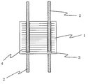
図7は太陽電池素子のバスバー電極上に接続タブを取り付けた状態を示したものである。図7において1は太陽電池素子、2は接続タブ、3はバスバー電極、4はフィンガー電極を示す。 FIG. 7 shows a state where a connection tab is attached on the bus bar electrode of the solar cell element. In FIG. 7, 1 is a solar cell element, 2 is a connection tab, 3 is a bus-bar electrode, 4 is a finger electrode.
太陽電池素子1は、例えば厚み0.3〜0.4mm程度、大きさ150mm角程度の単結晶シリコンや多結晶シリコンで作られている。この太陽電池素子1の内部にはボロンなどのP型不純物を多く含んだP層とリンなどのN型不純物を多く含んだN層が接しているPN接合(不図示)が形成されている。バスバー電極3とフィンガー電極4は、銀ペーストをスクリーンプリントすることなどにより形成され、またバスバー電極3の表面は、その保護と接続タブを取り付けやすくするために、そのほぼ全面にわたりハンダコートされることもある。またフィンガー電極4は幅0.1〜0.2mm程度で、太陽電池素子の辺に平行に、光生成キャリヤーを収集するため多数本形成される。またバスバー電極3は収集されたキャリヤーを集電し、接続タブを取り付けるために幅2mm程度で、フィンガー電極4と垂直に交わるように2本程度形成される。このようなバスバー電極3とフィンガー電極4は、太陽電池素子1の裏面(非受光面)側にも同様に形成されている。
The
接続タブ2は、太陽電池素子同士を互いに電気的に接続するものであり、銅などの低抵抗の金属箔をリボン状に切断し、この表面にハンダコートを施し、これを適当な長さに切断して用いている。
The
太陽電池モジュールにおいては、通常図7に示すように接続タブ2を太陽電池素子1の受光面と裏面のバスバー電極上にハンダ付けすることにより取り付け、この接続タブ2の他端部をさらに隣接する太陽電池素子に取り付けることにより太陽電池素子同士を電気的に接続している。
In the solar cell module, as shown in FIG. 7, the
(特許文献1の従来の技術参照)
この出願の発明に関連する先行技術文献情報としては次のようなものがある。
Prior art document information related to the invention of this application includes the following.
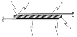
図8は、上述のように太陽電池素子の受光面と裏面の電極に接続タブをハンダ付けにより取り付けた状態を示す断面図である。 FIG. 8 is a cross-sectional view showing a state in which the connection tabs are attached to the electrodes on the light receiving surface and the back surface of the solar cell element by soldering as described above.
これにおいて、例えばまず太陽電池素子1の受光面に接続タブ2を取り付け時では、ハンダ付け時にその温度が200℃以上になるため、太陽電池素子のシリコン基板と接続タブの銅箔の熱膨張率の差により室温に戻ったときに太陽電池素子に反りが発生してしまう。
In this case, for example, when the
けれどもこれに続けて、太陽電池素子1の裏面にも同様に接続タブ2を取り付けるため、受光面と裏面の反りが互いに均衡し、打ち消されるため、結果として太陽電池素子1には、大きな反りは生じないこととなる。
However, subsequently, since the
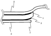
しかし接続タブ2の端部7においては、放熱し易いため、熱風を吹き付けること等によるハンダ付け時に接続タブ2の中央部より温度が上がりにくく、この接続タブ2の端部7はバスバー電極3とのハンダ付けができないことがあった。
However, since the
図9は、この接続タブ2の端部7のハンダ付けができなかったものの端部の状態を示した断面図である。図9に示すように例えば太陽電池素子1の裏面にハンダ付けした接続タブの端部7がバスバー電極3とハンダ付けされなかった場合、受光面のバスバー電極にハンダ付けされた接続タブ2の熱収縮のために、その端部のみ受光面側に反りが発生してしまう。上記と同じ理由で太陽電池素子の他の端部でも反対方向の反りが発生することとなる。
FIG. 9 is a cross-sectional view showing the state of the end of the
この様に太陽電池素子1の両端部に反りが発生すると、バスバー電極が太陽電池素子基板より剥離したり、またその後の太陽電池素子を充填材で封入するラミネート工程において、太陽電池素子が割れたり、クラックが発生することがあり、太陽電池モジュールの製造工程における歩留りを低下させる原因となる。
When warping occurs at both ends of the
特に最近の太陽電池モジュールでは、環境面への配慮から使用するハンダに鉛が実質的に含まれないものを使用するものが増えており、この鉛が実質的に含まれないハンダを使用した場合では、そのハンダの物性からハンダ付け温度が高くなるため、上記のような接続タブのハンダ付け前後で太陽電池素子の端部の反りの程度がさらに大きくなること多くある。 In particular, in recent solar cell modules, the use of solder that does not substantially contain lead is increasing due to environmental considerations. When using solder that does not substantially contain lead Then, since the soldering temperature increases due to the physical properties of the solder, the degree of warping of the end portion of the solar cell element is often further increased before and after soldering of the connection tab as described above.
さらに最近の太陽電池モジュールでは、コストダウンのために太陽電池素子に使用するシリコン基板の大きさが大きくなり、またその厚みを薄くする傾向にあるため、太陽電池素子の端部の反りの程度がさらに大きくなる要因となっている。 Further, in recent solar cell modules, the size of the silicon substrate used for the solar cell element is increased for cost reduction, and the thickness tends to be reduced. This is a factor that increases further.
本発明はこのような問題点に鑑みなされたものであり、その目的は接続タブを太陽電池素子上の電極にハンダ付けした場合に、太陽電池素子の両端部に反りの発生することを無くすることにより、歩留りの高い太陽電池モジュールを提供することにある。 The present invention has been made in view of such problems, and the object thereof is to eliminate the occurrence of warping at both ends of the solar cell element when the connection tab is soldered to the electrode on the solar cell element. Thus, it is to provide a solar cell module with a high yield.
上記の目的を達成するため、本発明の太陽電池モジュールは、隣接する2つの太陽電池素子の一方の太陽電池素子の受光面側バスバー電極と他方の太陽電池素子の裏面側バスバー電極とに接続タブをハンダ付けすることにより複数の前記太陽電池素子を電気的に接続した太陽電池モジュールにおいて、前記太陽電池素子の受光面側バスバー電極及び/または裏面側バスバー電極のそれぞれの長手方向の端部表面にハンダレジストを塗布したことを特徴とする。 In order to achieve the above object, the solar cell module of the present invention is connected to the light receiving surface side bus bar electrode of one solar cell element and the back side bus bar electrode of the other solar cell element of two adjacent solar cell elements. In a solar cell module in which a plurality of the solar cell elements are electrically connected by soldering, a light receiving surface side bus bar electrode and / or a back side bus bar electrode of the solar cell element are respectively attached to the surface of the longitudinal direction. A solder resist is applied.
またバスバー電極の端部表面に塗布されたハンダレジストが、前記バスバー電極の周囲まで延出して塗布されていることが望ましい。 Further, it is desirable that the solder resist applied to the end surface of the bus bar electrode is applied so as to extend to the periphery of the bus bar electrode.
本発明の太陽電池モジュールによれば、隣接する2つの太陽電池素子の一方の太陽電池素子の受光面側バスバー電極と他方の太陽電池素子の裏面側バスバー電極とに接続タブをハンダ付けすることにより複数の前記太陽電池素子を電気的に接続した太陽電池モジュールにおいて、前記太陽電池素子の受光面側バスバー電極及び/または裏面側バスバー電極のそれぞれの長手方向の端部表面にハンダレジストを塗布したことにより、受光面と裏面のバスバー電極で接続タブとハンダ付けされる端部の位置を合わせることが可能となる。これによりタブ付け後に太陽電池素子の端部に反りが発生することがなくなり、バスバー電極が剥離したり、ラミネート工程において、太陽電池素子が割れたり、クラックが発生することが無くなる。 According to the solar cell module of the present invention, the connection tab is soldered to the light-receiving surface side bus bar electrode of one solar cell element and the back side bus bar electrode of the other solar cell element of two adjacent solar cell elements. In the solar cell module in which a plurality of the solar cell elements are electrically connected, a solder resist is applied to each longitudinal end surface of the light receiving surface side bus bar electrode and / or the back side bus bar electrode of the solar cell element. Accordingly, it is possible to align the positions of the connection tabs and the soldered ends with the bus bar electrodes on the light receiving surface and the back surface. Accordingly, the end of the solar cell element is not warped after the tab is attached, and the bus bar electrode is not peeled off, and the solar cell element is not cracked or cracked in the laminating process.
またバスバー電極の端部表面に塗布されたハンダレジストが、このバスバー電極の周囲まで延出して塗布されていることにより、ハンダレジストがバスバー電極端部を押さえ込むため、バスバー電極が太陽電池素子から剥離するのを防ぐ効果を確実なものとすることができる。 Also, since the solder resist applied to the end surface of the bus bar electrode extends to the periphery of the bus bar electrode, the solder resist presses the end of the bus bar electrode, so the bus bar electrode is peeled off from the solar cell element. The effect which prevents it can be made reliable.
以下、本発明の実施の形態を添付図面を用いて説明する。 Hereinafter, embodiments of the present invention will be described with reference to the accompanying drawings.
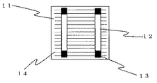
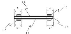
図1は本発明に係る太陽電池素子の受光面側の平面図である。また図2は本発明に係る太陽電池素子の断面図である。図1、図2において11は太陽電池素子、12は受光面バスバー電極、13はハンダレジスト、14は受光面フィンガー電極、15は裏面バスバー電極を示す。 FIG. 1 is a plan view of a light receiving surface side of a solar cell element according to the present invention. FIG. 2 is a cross-sectional view of the solar cell element according to the present invention. 1 and 2, 11 is a solar cell element, 12 is a light receiving surface bus bar electrode, 13 is a solder resist, 14 is a light receiving surface finger electrode, and 15 is a back surface bus bar electrode.
太陽電池素子11は、上述のように単結晶シリコンや多結晶シリコンで作られており、その受光面側と裏面側にバスバー電極12、15とフィンガー電極14が形成されている。
The solar cell element 11 is made of single crystal silicon or polycrystalline silicon as described above, and the
さらに本発明に係る太陽電池素子11では、受光面バスバー電極12と裏面バスバー電極15の両端部にハンダレジスト13が塗布されていることを特徴とする。
Furthermore, the solar cell element 11 according to the present invention is characterized in that a solder resist 13 is applied to both end portions of the light-receiving surface bus bar electrode 12 and the back surface
このハンダレジスト13は、例えばエポキシ樹脂などを主成分とするペースト状のもので、スクリーンプリントなどによりプリントされ、紫外線や熱などにより硬化される。硬化後のハンダレジストの膜厚は50〜100μm程度である。またこのハンダレジスト13はバスバー電極12、15の端部から5〜15mm程度の範囲にバスバー電極12、15の全面を覆うように塗布される。
The solder resist 13 is, for example, a paste having an epoxy resin as a main component, printed by screen printing or the like, and cured by ultraviolet rays or heat. The thickness of the cured solder resist is about 50 to 100 μm. The
またこのハンダレジスト13の塗布される位置は、受光面側と裏面側で太陽電池素子11の端部からハンダレジスト13の内側までの寸法(図2のaとa’及びbとb’)が同じになるようにする。
The
図3は、この本発明に係る太陽電池素子11に接続タブをハンダ付けする装置を示したものである。図3において17は熱風吹き出しノズル、18は押しつけピン、20は接続タブを示す。 FIG. 3 shows an apparatus for soldering a connection tab to the solar cell element 11 according to the present invention. In FIG. 3, 17 is a hot air blowing nozzle, 18 is a pressing pin, and 20 is a connection tab.
本発明に係る接続タブ20は、銅やアルミニウムのような低抵抗の太陽電池素子接続用配線材にハンダをその表面全面に片面20から70μm程度メッキやディピングによりハンダコートしたものを適当な長さに切断して用いる。この接続タブ20の幅は、ハンダ付け時に接続タブ20自身により太陽電池素子11の受光面に影を作らないように、太陽電池素子11のバスバー電極12の幅と同じかそれ以下にする。接続タブ20の長さは太陽電池素子11のバスバー電極12のほぼ全てに重なり、さらに所定の太陽電池素子間の間隔と隣り合う太陽電池素子の非受光面のバスバー電極に重なるようにする。一般的な150mm角の多結晶シリコン太陽電池素子を使用する場合、接続タブ20の幅は、1〜3mm程度、その長さは200〜300mm程度である。接続タブ20が太陽電池素子11のバスバー電極12のほぼ全てに重なるようにするのは、太陽電池素子の抵抗成分を少なくするためである。
The
接続タブ20の太陽電池素子11上のバスバー電極12、15への取り付けは、取り付ける太陽電池素子11のバスバー電極12の上へ接続タブ20を持ってくる。その後押しつけピン18を下ろし、接続タブ20をバスバー電極12に押しつける。それと同時にノズル17から、400から500℃程度の熱風を1、2秒程度、上記の押しつけピン18で接続タブ20をバスバー電極12に押しつけている部分に吹き付け、接続タブ20のハンダとバスバー電極12のハンダを融かし両者を接合する。その後ハンダが固化したら、押しつけピン18を上げる。この様にして太陽電池素子11の受光面側と裏面側のバスバー電極にそれぞれ接続タブをハンダ付けする。
The attachment of the
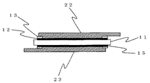
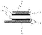
図4は、この本発明に係る太陽電池素子の受光面と裏面に接続タブをハンダ付けした状態を示す断面図である。図4に示すように太陽電池素子11の受光面側のバスバー電極12に接続タブ22をハンダ付けした場合、バスバー電極12の両端部には上記のようにハンダレジスト13が塗布してあるため、この部分に配置された接続タブ22はバスバー電極12とハンダ付けされることがない。これと同様に、太陽電池素子11の裏面側のバスバー電極15に接続タブ23をハンダ付けした場合も、バスバー電極15の両端部のハンダレジスト13が塗布してある部分には、接続タブ23とハンダ付けされることがない。
FIG. 4 is a cross-sectional view showing a state in which connection tabs are soldered to the light receiving surface and the back surface of the solar cell element according to the present invention. As shown in FIG. 4, when the
さらにここで上述のようにハンダレジスト13の塗布される位置は、受光面側と裏面側で太陽電池素子11の端部からハンダレジスト13の内側までの寸法が同じになるようにしたため、タブ付け後の太陽電池素子11において、接続タブ22、23の熱収縮による応力が受光面側と裏面側で均衡するため、太陽電池素子11の端部において反りが発生することがない。
Further, as described above, the solder resist 13 is applied to the light receiving surface side and the back surface side because the dimensions from the end of the solar cell element 11 to the inside of the solder resist 13 are the same. In the later solar cell element 11, the stress due to the thermal contraction of the
図5は本発明に係る別の実施例を示すものである。図5における実施例では、太陽電池素子11のバスバー電極12、15の端部表面に塗布されたハンダレジスト13が、このバスバー電極12、15の周囲まで延出して塗布されていることを特徴とする。
FIG. 5 shows another embodiment according to the present invention. The embodiment in FIG. 5 is characterized in that the solder resist 13 applied to the end surface of the
これによりバスバー電極12、15の端部がハンダレジスト13に覆われると共にハンダレジスト13が太陽電池素子11の基板表面にまで延出することにより、バスバー電極12、15の端部がハンダレジスト13により太陽電池素子11の基板表面に接着される形となる。
As a result, the end portions of the
これによりバスバー電極12、15が太陽電池素子11からの剥離を防止するという本発明の効果を確実なものにすることが可能となる。
This makes it possible to ensure the effect of the present invention that the
本発明に係る太陽電池モジュールの製造工程においては、一般に上述のように接続タブを用いて複数個(通常4〜10個程度)の太陽電池素子を直線的に直列に接続して太陽電池ストリングを作製し、さらにこの太陽電池ストリング同士をさらに太陽電池モジュールの定格出力に合うように電気的に接続している。 In the manufacturing process of the solar cell module according to the present invention, generally, a plurality of (usually about 4 to 10) solar cell elements are linearly connected in series using a connection tab as described above to form a solar cell string. Further, the solar cell strings are further electrically connected so as to match the rated output of the solar cell module.
図6は本発明に係る太陽電池モジュールの構造の一例を示す図である。 FIG. 6 is a diagram showing an example of the structure of the solar cell module according to the present invention.
図6において、31は透光性基板、32は受光面側充填材、33は太陽電池ストリング、34は裏面側充填材、35は裏面シート、36は接続タブである。 In FIG. 6, 31 is a translucent substrate, 32 is a light receiving surface side filler, 33 is a solar cell string, 34 is a back surface side filler, 35 is a back sheet, and 36 is a connection tab.
以下、各部材について説明する。 Hereinafter, each member will be described.
透光性基板31としては、ガラスやポリカーボネート樹脂などからなる基板が用いられる。ガラス板ついては、白板ガラス、強化ガラス、倍強化ガラス、熱線反射ガラスなどが用いられるが、一般的には厚さ3mm〜5mm程度の白板強化ガラスが使用される。他方、ポリカーボネート樹脂などの合成樹脂からなる基板を用いた場合には、厚みが5mm程度のものが多く使用される。 As the translucent substrate 31, a substrate made of glass, polycarbonate resin, or the like is used. As for the glass plate, white plate glass, tempered glass, double tempered glass, heat ray reflective glass and the like are used, but generally white plate tempered glass having a thickness of about 3 mm to 5 mm is used. On the other hand, when a substrate made of a synthetic resin such as polycarbonate resin is used, a substrate having a thickness of about 5 mm is often used.
受光面側充填材32及び裏面側充填材34は、エチレン−酢酸ビニル共重合体(以下EVAと略す)やポリビニルブチラール(PVB)から成り、Tダイと押し出し機により厚さ0.4〜1mm程度のシート状に成形されたものが用いられる。これらはラミネート装置により減圧下にて加熱加圧を行うことで、軟化、融着して他の部材と一体化する。
The light receiving
EVAやPVBは、酸化チタンや顔料等を含有させ白色等に着色させることがあるが、本発明に係る太陽電池モジュールの製造方法における受光面側充填材32においては、着色させると太陽電池素子33に入射する光量が減少し、発電効率が低下するため透明とする。
EVA and PVB may contain titanium oxide, pigment, or the like to be colored white, etc., but in the light receiving
また、裏面側充填材34に用いるEVAやPVBは透明でも構わないし、太陽電池モジュールの設置される周囲の設置環境に合わせ酸化チタンや顔料等を含有させ白色等に着色させても構わない。
Further, EVA or PVB used for the back
裏面シート35は水分を透過しないようにアルミ箔を挟持した耐候性を有するフッ素系樹脂シートやアルミナまたはシリカを蒸着したポリエチレンテレフタレ−ト(PET)シートなどが用いられる。 As the back sheet 35, a fluorine-based resin sheet having weather resistance in which an aluminum foil is sandwiched so as not to transmit moisture, a polyethylene terephthalate (PET) sheet on which alumina or silica is deposited, and the like are used.
次に太陽電池モジュールの作製方法について述べる。 Next, a method for manufacturing a solar cell module will be described.
太陽電池モジュールを作製するにあたっては、透光性基板31上に受光面側充填材32を置き、さらにその上に接続タブ36等で接続した太陽電池ストリング33を置く。さらにその上に裏面側充填材34、裏面シート35を順次積層する。このような状態にして、ラミネーターにセットし、減圧下にて加圧しながら100〜200℃で例えば15分〜1時間加熱することにより、これらが一体化する。
In producing the solar cell module, the light receiving
なお、本発明は上記実施形態に限定されるものではなく、本発明の範囲内で多くの修正及び変更を加えることができる。例えば太陽電池素子は単結晶や多結晶シリコンなどの結晶系太陽電池に限定されるものではなく、薄膜系太陽電池などでも適用可能である。 In addition, this invention is not limited to the said embodiment, Many corrections and changes can be added within the scope of the present invention. For example, the solar cell element is not limited to a crystalline solar cell such as a single crystal or polycrystalline silicon, and can be applied to a thin film solar cell.
またハンダ付けに使用するハンダは、錫−鉛の共晶ハンダ等の他鉛フリーハンダでも実施可能である。 The solder used for soldering can also be implemented by lead-free solder such as tin-lead eutectic solder.
さらに本発明に係る太陽電池モジュール製造方法においては、太陽電池ストリング作製工程で接続タブにより複数の太陽電池素子が接続され太陽電池ストリングが完成してからこの太陽電池ストリングが上記のラミネート工程での加圧されるまでに3時間以上、望ましくは15時間以上室温にて放置することを特徴とする。 Furthermore, in the solar cell module manufacturing method according to the present invention, the solar cell string is added in the laminating step after the solar cell string is completed by connecting a plurality of solar cell elements by the connection tab in the solar cell string manufacturing step. It is characterized by being allowed to stand at room temperature for 3 hours or more, preferably 15 hours or more before being pressed.
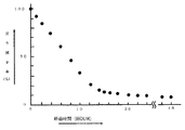
図10は、発明者らが繰り返し行った多結晶太陽電池ストリング作製後の時間経過と反りの程度をまとめたグラフである。図10において縦軸は、太陽電池ストリング作製直後の太陽電池素子の反りの大きさを100%として、その後室温にこの太陽電池ストリングを室温に放置した時の時間経過を示すものである。 FIG. 10 is a graph summarizing the time course and the degree of warping after the inventors repeatedly made a polycrystalline solar cell string. In FIG. 10, the vertical axis indicates the time elapsed when the solar cell string is left at room temperature at room temperature after setting the amount of warpage of the solar cell element immediately after the solar cell string to be 100%.
このグラフから解るように、太陽電池ストリング作製直後から3時間後では反りは60%程に減少しており、この60%まで減少した反りの太陽電池素子を前記ラミネート工程で加圧した場合では、これにおける太陽電池素子の割れやクラックの発生は太陽電池ストリング作製直後のものに比べ、およそ半分に低下させることができる。これによって太陽電池モジュールを高い歩留まりで作製できる。 As can be seen from this graph, the warpage is reduced to about 60% 3 hours after the solar cell string is produced, and when the solar cell element having the warpage reduced to 60% is pressed in the laminating step, The occurrence of cracks and cracks in the solar cell element can be reduced to about half compared to that immediately after the production of the solar cell string. Thereby, a solar cell module can be manufactured with a high yield.
さらに太陽電池ストリング作製直後から15時間まではほぼ直線的に太陽電池素子の反りは減少しているが、それ以降はほとんど減少していない。この傾向は太陽電池素子の厚みや大きさなどに関係なく一定であった。 Further, the warpage of the solar cell element decreases almost linearly from immediately after the production of the solar cell string to 15 hours, but hardly decreases thereafter. This tendency was constant regardless of the thickness and size of the solar cell element.
すなわち、作製された太陽電池ストリングが前記ラミネート工程で加圧されるまでに3時間好ましくは15時間以上室温にて放置することにより太陽電池素子のシリコン基板と電極部等との熱膨張率の違いにより発生する反りがほぼ接続タブをハンダ付け前の状態に戻り、反りの程度が大幅に小さくなる。これによりラミネート工程での割れやクラックの発生を大幅に低減することが可能となる。 That is, the difference in the thermal expansion coefficient between the silicon substrate of the solar cell element and the electrode part, etc. by leaving the produced solar cell string at room temperature for 3 hours, preferably 15 hours or more before being pressed in the laminating step. The warpage caused by the above-mentioned almost returns to the state before the connection tab is soldered, and the degree of warpage is greatly reduced. Thereby, it becomes possible to greatly reduce the occurrence of cracks and cracks in the laminating process.
1、11、33;太陽電池素子
2、20、22、23、36;接続タブ
3;バスバー電極
4;フィンガー電極
7;接続タブの端部
12;受光面バスバー電極
13;ハンダレジスト
14;受光面フィンガー電極
15;裏面バスバー電極
17;熱風吹き出しノズル
18;押しつけピン
31;透光性基板
32;受光面側充填材
34;裏面側充填材
35;裏面シート
1, 11, 33;
Claims (2)
Priority Applications (1)
| Application Number | Priority Date | Filing Date | Title |
|---|---|---|---|
| JP2005343622A JP2007123792A (en) | 2005-09-28 | 2005-11-29 | Solar battery module |
Applications Claiming Priority (2)
| Application Number | Priority Date | Filing Date | Title |
|---|---|---|---|
| JP2005281966 | 2005-09-28 | ||
| JP2005343622A JP2007123792A (en) | 2005-09-28 | 2005-11-29 | Solar battery module |
Publications (1)
| Publication Number | Publication Date |
|---|---|
| JP2007123792A true JP2007123792A (en) | 2007-05-17 |
Family
ID=38147260
Family Applications (1)
| Application Number | Title | Priority Date | Filing Date |
|---|---|---|---|
| JP2005343622A Pending JP2007123792A (en) | 2005-09-28 | 2005-11-29 | Solar battery module |
Country Status (1)
| Country | Link |
|---|---|
| JP (1) | JP2007123792A (en) |
Cited By (10)
| Publication number | Priority date | Publication date | Assignee | Title |
|---|---|---|---|---|
| JP2011066037A (en) * | 2009-09-15 | 2011-03-31 | Dainippon Screen Mfg Co Ltd | Method and device for forming pattern |
| US20140196768A1 (en) * | 2013-01-11 | 2014-07-17 | Silevo, Inc. | Module fabrication of solar cells with low resistivity electrodes |
| US20150270410A1 (en) * | 2013-01-11 | 2015-09-24 | Silevo, Inc. | Module fabrication of solar cells with low resistivity electrodes |
| RU2663543C1 (en) * | 2017-08-31 | 2018-08-07 | Общество с ограниченной ответственностью "НТЦ тонкопленочных технологий в энергетике", ООО "НТЦ ТПТ" | Method for assembling solar modules a monolithic solar module from cells of photoelectric converters by using an adhesive layer |
| US10084099B2 (en) | 2009-11-12 | 2018-09-25 | Tesla, Inc. | Aluminum grid as backside conductor on epitaxial silicon thin film solar cells |
| US10115838B2 (en) | 2016-04-19 | 2018-10-30 | Tesla, Inc. | Photovoltaic structures with interlocking busbars |
| US10181536B2 (en) | 2015-10-22 | 2019-01-15 | Tesla, Inc. | System and method for manufacturing photovoltaic structures with a metal seed layer |
| US10309012B2 (en) | 2014-07-03 | 2019-06-04 | Tesla, Inc. | Wafer carrier for reducing contamination from carbon particles and outgassing |
| US10672919B2 (en) | 2017-09-19 | 2020-06-02 | Tesla, Inc. | Moisture-resistant solar cells for solar roof tiles |
| US11190128B2 (en) | 2018-02-27 | 2021-11-30 | Tesla, Inc. | Parallel-connected solar roof tile modules |
-
2005
- 2005-11-29 JP JP2005343622A patent/JP2007123792A/en active Pending
Cited By (14)
| Publication number | Priority date | Publication date | Assignee | Title |
|---|---|---|---|---|
| JP2011066037A (en) * | 2009-09-15 | 2011-03-31 | Dainippon Screen Mfg Co Ltd | Method and device for forming pattern |
| US10084099B2 (en) | 2009-11-12 | 2018-09-25 | Tesla, Inc. | Aluminum grid as backside conductor on epitaxial silicon thin film solar cells |
| US9219174B2 (en) * | 2013-01-11 | 2015-12-22 | Solarcity Corporation | Module fabrication of solar cells with low resistivity electrodes |
| US20150270410A1 (en) * | 2013-01-11 | 2015-09-24 | Silevo, Inc. | Module fabrication of solar cells with low resistivity electrodes |
| US9412884B2 (en) * | 2013-01-11 | 2016-08-09 | Solarcity Corporation | Module fabrication of solar cells with low resistivity electrodes |
| US20140196768A1 (en) * | 2013-01-11 | 2014-07-17 | Silevo, Inc. | Module fabrication of solar cells with low resistivity electrodes |
| US10115839B2 (en) | 2013-01-11 | 2018-10-30 | Tesla, Inc. | Module fabrication of solar cells with low resistivity electrodes |
| US10164127B2 (en) | 2013-01-11 | 2018-12-25 | Tesla, Inc. | Module fabrication of solar cells with low resistivity electrodes |
| US10309012B2 (en) | 2014-07-03 | 2019-06-04 | Tesla, Inc. | Wafer carrier for reducing contamination from carbon particles and outgassing |
| US10181536B2 (en) | 2015-10-22 | 2019-01-15 | Tesla, Inc. | System and method for manufacturing photovoltaic structures with a metal seed layer |
| US10115838B2 (en) | 2016-04-19 | 2018-10-30 | Tesla, Inc. | Photovoltaic structures with interlocking busbars |
| RU2663543C1 (en) * | 2017-08-31 | 2018-08-07 | Общество с ограниченной ответственностью "НТЦ тонкопленочных технологий в энергетике", ООО "НТЦ ТПТ" | Method for assembling solar modules a monolithic solar module from cells of photoelectric converters by using an adhesive layer |
| US10672919B2 (en) | 2017-09-19 | 2020-06-02 | Tesla, Inc. | Moisture-resistant solar cells for solar roof tiles |
| US11190128B2 (en) | 2018-02-27 | 2021-11-30 | Tesla, Inc. | Parallel-connected solar roof tile modules |
Similar Documents
| Publication | Publication Date | Title |
|---|---|---|
| JP2006278710A (en) | Solar battery module and manufacturing method thereof | |
| JP2007123792A (en) | Solar battery module | |
| WO2010116973A1 (en) | Interconnect sheet, solar cell with interconnect sheet, solar module, and method of producing solar cell with interconnect sheet | |
| JP5016342B2 (en) | Solar cell module | |
| JP5879513B2 (en) | Solar cell module | |
| EP2216827A1 (en) | Solar battery module and method for manufacturing solar battery module | |
| JP2009246208A (en) | Solar cell module, and method for manufacturing the same | |
| JP4738147B2 (en) | Solar cell module and manufacturing method thereof | |
| JP2008010857A (en) | Solar cell module | |
| JP2005191125A (en) | Connection tab for connecting solar battery element and solar battery module, and method of manufacturing solar battery module | |
| JP2005159173A (en) | Wiring material for connecting solar cell element and solar cell module | |
| JP4667098B2 (en) | Solar cell module | |
| JP2007201291A (en) | Solar battery module and method of reproducing same | |
| JP4454322B2 (en) | Solar cell module | |
| JP2006278695A (en) | Solar cell module | |
| JP2004281797A (en) | Solar cell module | |
| JP4340132B2 (en) | Manufacturing method of solar cell module | |
| EP2579318A1 (en) | Photovoltaic cell module and photovoltaic cell | |
| JP2007123522A (en) | Method of manufacturing solar cell module | |
| JP5153361B2 (en) | Repair method of solar cell module | |
| JP4883891B2 (en) | Solar cell module | |
| JP6163014B2 (en) | Manufacturing method of solar cell module | |
| JP2005236217A (en) | Sealing material for solar cell module, and manufacturing method for solar cell module using the same | |
| JP2006073706A (en) | Solar cell module | |
| JP2004327630A (en) | Solar cell module |