JP2007081233A - Laser oscillator - Google Patents
Laser oscillator Download PDFInfo
- Publication number
- JP2007081233A JP2007081233A JP2005268845A JP2005268845A JP2007081233A JP 2007081233 A JP2007081233 A JP 2007081233A JP 2005268845 A JP2005268845 A JP 2005268845A JP 2005268845 A JP2005268845 A JP 2005268845A JP 2007081233 A JP2007081233 A JP 2007081233A
- Authority
- JP
- Japan
- Prior art keywords
- crystal
- laser
- film
- dielectric
- wavelength conversion
- Prior art date
- Legal status (The legal status is an assumption and is not a legal conclusion. Google has not performed a legal analysis and makes no representation as to the accuracy of the status listed.)
- Pending
Links
Images


Classifications
-
- H—ELECTRICITY
- H01—ELECTRIC ELEMENTS
- H01S—DEVICES USING THE PROCESS OF LIGHT AMPLIFICATION BY STIMULATED EMISSION OF RADIATION [LASER] TO AMPLIFY OR GENERATE LIGHT; DEVICES USING STIMULATED EMISSION OF ELECTROMAGNETIC RADIATION IN WAVE RANGES OTHER THAN OPTICAL
- H01S3/00—Lasers, i.e. devices using stimulated emission of electromagnetic radiation in the infrared, visible or ultraviolet wave range
- H01S3/10—Controlling the intensity, frequency, phase, polarisation or direction of the emitted radiation, e.g. switching, gating, modulating or demodulating
- H01S3/106—Controlling the intensity, frequency, phase, polarisation or direction of the emitted radiation, e.g. switching, gating, modulating or demodulating by controlling devices placed within the cavity
- H01S3/108—Controlling the intensity, frequency, phase, polarisation or direction of the emitted radiation, e.g. switching, gating, modulating or demodulating by controlling devices placed within the cavity using non-linear optical devices, e.g. exhibiting Brillouin or Raman scattering
- H01S3/109—Frequency multiplication, e.g. harmonic generation
-
- H—ELECTRICITY
- H01—ELECTRIC ELEMENTS
- H01S—DEVICES USING THE PROCESS OF LIGHT AMPLIFICATION BY STIMULATED EMISSION OF RADIATION [LASER] TO AMPLIFY OR GENERATE LIGHT; DEVICES USING STIMULATED EMISSION OF ELECTROMAGNETIC RADIATION IN WAVE RANGES OTHER THAN OPTICAL
- H01S3/00—Lasers, i.e. devices using stimulated emission of electromagnetic radiation in the infrared, visible or ultraviolet wave range
- H01S3/23—Arrangements of two or more lasers not provided for in groups H01S3/02 - H01S3/22, e.g. tandem arrangements of separate active media
- H01S3/2383—Parallel arrangements
-
- G—PHYSICS
- G02—OPTICS
- G02F—OPTICAL DEVICES OR ARRANGEMENTS FOR THE CONTROL OF LIGHT BY MODIFICATION OF THE OPTICAL PROPERTIES OF THE MEDIA OF THE ELEMENTS INVOLVED THEREIN; NON-LINEAR OPTICS; FREQUENCY-CHANGING OF LIGHT; OPTICAL LOGIC ELEMENTS; OPTICAL ANALOGUE/DIGITAL CONVERTERS
- G02F1/00—Devices or arrangements for the control of the intensity, colour, phase, polarisation or direction of light arriving from an independent light source, e.g. switching, gating or modulating; Non-linear optics
- G02F1/35—Non-linear optics
- G02F1/353—Frequency conversion, i.e. wherein a light beam is generated with frequency components different from those of the incident light beams
- G02F1/3542—Multipass arrangements, i.e. arrangements to make light pass multiple times through the same element, e.g. using an enhancement cavity
-
- H—ELECTRICITY
- H01—ELECTRIC ELEMENTS
- H01S—DEVICES USING THE PROCESS OF LIGHT AMPLIFICATION BY STIMULATED EMISSION OF RADIATION [LASER] TO AMPLIFY OR GENERATE LIGHT; DEVICES USING STIMULATED EMISSION OF ELECTROMAGNETIC RADIATION IN WAVE RANGES OTHER THAN OPTICAL
- H01S3/00—Lasers, i.e. devices using stimulated emission of electromagnetic radiation in the infrared, visible or ultraviolet wave range
- H01S3/02—Constructional details
- H01S3/025—Constructional details of solid state lasers, e.g. housings or mountings
-
- H—ELECTRICITY
- H01—ELECTRIC ELEMENTS
- H01S—DEVICES USING THE PROCESS OF LIGHT AMPLIFICATION BY STIMULATED EMISSION OF RADIATION [LASER] TO AMPLIFY OR GENERATE LIGHT; DEVICES USING STIMULATED EMISSION OF ELECTROMAGNETIC RADIATION IN WAVE RANGES OTHER THAN OPTICAL
- H01S3/00—Lasers, i.e. devices using stimulated emission of electromagnetic radiation in the infrared, visible or ultraviolet wave range
- H01S3/02—Constructional details
- H01S3/04—Arrangements for thermal management
- H01S3/0405—Conductive cooling, e.g. by heat sinks or thermo-electric elements
-
- H—ELECTRICITY
- H01—ELECTRIC ELEMENTS
- H01S—DEVICES USING THE PROCESS OF LIGHT AMPLIFICATION BY STIMULATED EMISSION OF RADIATION [LASER] TO AMPLIFY OR GENERATE LIGHT; DEVICES USING STIMULATED EMISSION OF ELECTROMAGNETIC RADIATION IN WAVE RANGES OTHER THAN OPTICAL
- H01S3/00—Lasers, i.e. devices using stimulated emission of electromagnetic radiation in the infrared, visible or ultraviolet wave range
- H01S3/02—Constructional details
- H01S3/04—Arrangements for thermal management
- H01S3/042—Arrangements for thermal management for solid state lasers
-
- H—ELECTRICITY
- H01—ELECTRIC ELEMENTS
- H01S—DEVICES USING THE PROCESS OF LIGHT AMPLIFICATION BY STIMULATED EMISSION OF RADIATION [LASER] TO AMPLIFY OR GENERATE LIGHT; DEVICES USING STIMULATED EMISSION OF ELECTROMAGNETIC RADIATION IN WAVE RANGES OTHER THAN OPTICAL
- H01S3/00—Lasers, i.e. devices using stimulated emission of electromagnetic radiation in the infrared, visible or ultraviolet wave range
- H01S3/05—Construction or shape of optical resonators; Accommodation of active medium therein; Shape of active medium
- H01S3/06—Construction or shape of active medium
- H01S3/0602—Crystal lasers or glass lasers
- H01S3/0604—Crystal lasers or glass lasers in the form of a plate or disc
-
- H—ELECTRICITY
- H01—ELECTRIC ELEMENTS
- H01S—DEVICES USING THE PROCESS OF LIGHT AMPLIFICATION BY STIMULATED EMISSION OF RADIATION [LASER] TO AMPLIFY OR GENERATE LIGHT; DEVICES USING STIMULATED EMISSION OF ELECTROMAGNETIC RADIATION IN WAVE RANGES OTHER THAN OPTICAL
- H01S3/00—Lasers, i.e. devices using stimulated emission of electromagnetic radiation in the infrared, visible or ultraviolet wave range
- H01S3/05—Construction or shape of optical resonators; Accommodation of active medium therein; Shape of active medium
- H01S3/08—Construction or shape of optical resonators or components thereof
- H01S3/08086—Multiple-wavelength emission
- H01S3/0809—Two-wavelenghth emission
-
- H—ELECTRICITY
- H01—ELECTRIC ELEMENTS
- H01S—DEVICES USING THE PROCESS OF LIGHT AMPLIFICATION BY STIMULATED EMISSION OF RADIATION [LASER] TO AMPLIFY OR GENERATE LIGHT; DEVICES USING STIMULATED EMISSION OF ELECTROMAGNETIC RADIATION IN WAVE RANGES OTHER THAN OPTICAL
- H01S3/00—Lasers, i.e. devices using stimulated emission of electromagnetic radiation in the infrared, visible or ultraviolet wave range
- H01S3/05—Construction or shape of optical resonators; Accommodation of active medium therein; Shape of active medium
- H01S3/08—Construction or shape of optical resonators or components thereof
- H01S3/081—Construction or shape of optical resonators or components thereof comprising three or more reflectors
- H01S3/0813—Configuration of resonator
- H01S3/0815—Configuration of resonator having 3 reflectors, e.g. V-shaped resonators
-
- H—ELECTRICITY
- H01—ELECTRIC ELEMENTS
- H01S—DEVICES USING THE PROCESS OF LIGHT AMPLIFICATION BY STIMULATED EMISSION OF RADIATION [LASER] TO AMPLIFY OR GENERATE LIGHT; DEVICES USING STIMULATED EMISSION OF ELECTROMAGNETIC RADIATION IN WAVE RANGES OTHER THAN OPTICAL
- H01S3/00—Lasers, i.e. devices using stimulated emission of electromagnetic radiation in the infrared, visible or ultraviolet wave range
- H01S3/05—Construction or shape of optical resonators; Accommodation of active medium therein; Shape of active medium
- H01S3/08—Construction or shape of optical resonators or components thereof
- H01S3/081—Construction or shape of optical resonators or components thereof comprising three or more reflectors
- H01S3/082—Construction or shape of optical resonators or components thereof comprising three or more reflectors defining a plurality of resonators, e.g. for mode selection or suppression
-
- H—ELECTRICITY
- H01—ELECTRIC ELEMENTS
- H01S—DEVICES USING THE PROCESS OF LIGHT AMPLIFICATION BY STIMULATED EMISSION OF RADIATION [LASER] TO AMPLIFY OR GENERATE LIGHT; DEVICES USING STIMULATED EMISSION OF ELECTROMAGNETIC RADIATION IN WAVE RANGES OTHER THAN OPTICAL
- H01S3/00—Lasers, i.e. devices using stimulated emission of electromagnetic radiation in the infrared, visible or ultraviolet wave range
- H01S3/09—Processes or apparatus for excitation, e.g. pumping
- H01S3/091—Processes or apparatus for excitation, e.g. pumping using optical pumping
- H01S3/094—Processes or apparatus for excitation, e.g. pumping using optical pumping by coherent light
- H01S3/0941—Processes or apparatus for excitation, e.g. pumping using optical pumping by coherent light of a laser diode
- H01S3/09415—Processes or apparatus for excitation, e.g. pumping using optical pumping by coherent light of a laser diode the pumping beam being parallel to the lasing mode of the pumped medium, e.g. end-pumping
-
- H—ELECTRICITY
- H01—ELECTRIC ELEMENTS
- H01S—DEVICES USING THE PROCESS OF LIGHT AMPLIFICATION BY STIMULATED EMISSION OF RADIATION [LASER] TO AMPLIFY OR GENERATE LIGHT; DEVICES USING STIMULATED EMISSION OF ELECTROMAGNETIC RADIATION IN WAVE RANGES OTHER THAN OPTICAL
- H01S3/00—Lasers, i.e. devices using stimulated emission of electromagnetic radiation in the infrared, visible or ultraviolet wave range
- H01S3/10—Controlling the intensity, frequency, phase, polarisation or direction of the emitted radiation, e.g. switching, gating, modulating or demodulating
- H01S3/102—Controlling the intensity, frequency, phase, polarisation or direction of the emitted radiation, e.g. switching, gating, modulating or demodulating by controlling the active medium, e.g. by controlling the processes or apparatus for excitation
- H01S3/1022—Controlling the intensity, frequency, phase, polarisation or direction of the emitted radiation, e.g. switching, gating, modulating or demodulating by controlling the active medium, e.g. by controlling the processes or apparatus for excitation by controlling the optical pumping
Landscapes
- Physics & Mathematics (AREA)
- Electromagnetism (AREA)
- Engineering & Computer Science (AREA)
- Plasma & Fusion (AREA)
- Optics & Photonics (AREA)
- Nonlinear Science (AREA)
- Lasers (AREA)
- Optical Modulation, Optical Deflection, Nonlinear Optics, Optical Demodulation, Optical Logic Elements (AREA)
Abstract
Description
本発明は、半導体レーザを励起源としたレーザ発振装置に関するものである。 The present invention relates to a laser oscillation device using a semiconductor laser as an excitation source.
先ず、レーザ発振装置1の概略を説明する。 First, an outline of the laser oscillation device 1 will be described.
図7はレーザ発振装置1の一例である、1波長発振のLD励起固体レーザを示している。 FIG. 7 shows an LD-pumped solid-state laser with one wavelength oscillation, which is an example of the laser oscillation device 1.
図7中、2は発光部、3は光共振部である。前記発光部2はLD発光器4、集光レンズ5を具備し、更に前記光共振部3は第1誘電体反射膜7が形成された第1光学結晶(レーザ結晶8)、第2光学結晶(非線形光学結晶(NLO)(波長変換結晶9))、第2誘電体反射膜11が形成された凹面鏡12を具備し、前記光共振部3に於いてレーザ光線をポンピングし、共振、増幅して出力している。尚、前記レーザ結晶8としては、Nd:YVO4 、前記波長変換結晶9としてはKTP(KTiOPO4 リン酸チタニルカリウム)が挙げられる。
In FIG. 7, 2 is a light emission part, 3 is an optical resonance part. The
更に説明すると以下の通りである。 Further description is as follows.
レーザ発振装置1は、例えば波長809nmのレーザ光線を射出する為のものであり、半導体レーザである前記LD発光器4が使用されている。又、該LD発光器4が励起光を発生させるポンプ光発生装置としての機能を有する。尚、前記レーザ発振装置1は半導体レーザに限ることなく、レーザ光線を生じさせることができれば、何れの光源手段をも採用することができる。 The laser oscillation device 1 is for emitting a laser beam having a wavelength of 809 nm, for example, and the LD light emitter 4 which is a semiconductor laser is used. Further, the LD light emitter 4 has a function as a pump light generator for generating excitation light. The laser oscillation device 1 is not limited to a semiconductor laser, and any light source means can be adopted as long as it can generate a laser beam.
前記レーザ結晶8は光の増幅を行う為のものである。該レーザ結晶8には、発振線が1064nmのNd:YVO4 が使用される。その他、Nd3+イオンをドープしたYAG(イットリウム アルミニウム ガーネット)等が採用され、YAGは、946nm、1064nm、1319nm等の発振線を有している。又、発振線が700nm〜900nmのTi(Sapphire)等を使用することができる。
The
前記レーザ結晶8の前記LD発光器4側には、前記第1誘電体反射膜7が形成されている。該第1誘電体反射膜7は、前記LD発光器4からのレーザ光線に対して高透過であり、且つ前記レーザ結晶8の発振波長に対して高反射であると共に、2次高調波(SHG:SECOND HARMONIC GENERATION)に対しても高反射となっている。
The first
前記凹面鏡12は、前記レーザ結晶8に対向する様に構成されており、前記凹面鏡12のレーザ結晶8側は、適宜の半径を有する凹面球面鏡の形状に加工されており、前記第2誘電体反射膜11が形成されている。該第2誘電体反射膜11は、前記レーザ結晶8の発振波長に対して高反射であり、2次高調波に対して高透過となっている。
The
以上の様に、前記レーザ結晶8の前記第1誘電体反射膜7と、前記凹面鏡12の前記第2誘電体反射膜11とを組合わせ、前記LD発光器4からのレーザ光線を前記集光レンズ5を介して前記レーザ結晶8にポンピングさせると、該レーザ結晶8の前記第1誘電体反射膜7と、前記第2誘電体反射膜11との間で光が往復し、光を長時間閉込めることができるので、光を共振させて増幅させることができる。
As described above, the first
前記レーザ結晶8の前記第1誘電体反射膜7と、前記凹面鏡12とから構成された光共振器内に前記波長変換結晶9が挿入されている。該波長変換結晶9にレーザ光線の様に強力なコヒーレント光が入射すると、光周波数を2倍にする2次高調波が発生する。該2次高調波の発生は、SECOND HARMONIC GENERATIONと呼ばれている。従って、前記レーザ発振装置1からは波長532nmのレーザ光線が射出される。
The
前記したレーザ発振装置1は前記波長変換結晶9を、前記レーザ結晶8と前記凹面鏡12とから構成された光共振器内に挿入しているので、内部型SHGと呼ばれており、変換出力は、励起光電力の2乗に比例するので、光共振器内の大きな光強度を直接利用できるという効果がある。
The laser oscillation device 1 is called an internal SHG because the
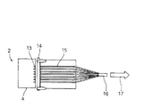
一般的に半導体レーザには大出力のレーザ光線を射出するものはなく、従って前記LD発光器4からのレーザ光線を励起光とするLD励起固体レーザとしても大きな出力は得られないものであるが、近年の大出力化の要望に対応して、LD発光器4を複数の半導体レーザ13で構成したものがある。 In general, there is no semiconductor laser that emits a high-power laser beam, and therefore a large output cannot be obtained as an LD-pumped solid-state laser that uses the laser beam from the LD emitter 4 as pump light. In response to the recent demand for higher output, there is one in which the LD light emitter 4 is composed of a plurality of semiconductor lasers 13.
例えば、特許文献1に示されるレーザ発振装置では、図8に示される様に、前記LD発光器4が複数の半導体レーザ13を具備し、該複数の半導体レーザ13をアレイ状に配設し、各半導体レーザ13から射出されたレーザ光線をロッドレンズ14で対応する光ファイバ15に集光させ、該光ファイバ15を束ねてファイバケーブル16とし高光強度の励起光17として前記レーザ結晶8に入射させ、高出力化を図っている。
For example, in the laser oscillation device disclosed in Patent Document 1, as shown in FIG. 8, the LD light emitter 4 includes a plurality of semiconductor lasers 13, and the plurality of semiconductor lasers 13 are arranged in an array, A laser beam emitted from each semiconductor laser 13 is condensed on a corresponding
該レーザ結晶8に前記励起光17を入射させると、前記レーザ結晶8に吸収されて該レーザ結晶8の端面で励起発振し、又吸収されなかった励起光17のエネルギの一部が熱となる。この為、端面励起型のレーザ発振装置では前記レーザ結晶8の入射端面が最も温度が上昇する。又、放熱されなかった熱は、前記レーザ結晶8内に蓄熱され、該レーザ結晶8の温度を上昇させる。
When the
該レーザ結晶8に入射させる励起光の光強度、即ち励起光のエネルギ密度が増大すると、前記レーザ結晶8の温度、特に入射端面温度が局部的に上昇し、而もレーザ結晶8自体熱伝導性は悪いので、光学的、機械的な歪みが生じ、レーザ発振しなくなる虞れがあり、又更に歪みが増大することで結晶の破壊に至る虞れが生じる。
When the light intensity of the excitation light incident on the
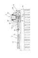
励起光の光強度の増大に起因する前記レーザ結晶8、前記波長変換結晶9の温度上昇に対して、前記レーザ結晶8、前記波長変換結晶9を冷却することが行われており、特許文献1では図9で示される冷却構造を有している。尚、図9中、図7、図8中で示したものと同等のものには同符号を付してある。
The
前記発光部2、前記光共振部3はヒートシンクであるベース19に固着され、前記発光部2、前記光共振部3は光軸10(図7参照)上に配設され、前記発光部2と前記光共振部3との間には前記集光レンズ5を含むレンズユニット21が配設されている。
The
前記ベース19に光共振器ブロック22が固着され、該光共振器ブロック22は前記光軸10上に前記レーザ結晶8を具備し、前記光共振器ブロック22の反レンズユニット21側には前記凹面鏡12が設けられている。
An
前記光共振器ブロック22には上方から凹部23が形成され、該凹部23内には波長変換結晶ホルダ24に保持された前記波長変換結晶9が収納されている。前記波長変換結晶ホルダ24は、球面座25を介して前記光共振器ブロック22に傾動可能に取付けられており、前記光軸10と前記波長変換結晶ホルダ24との光軸合せが可能となっている。又、前記光共振器ブロック22には前記波長変換結晶9を冷却する為のペルチェ素子26が設けられている。
The
前記レーザ結晶8の熱は、前記光共振器ブロック22を介して前記ベース19から放熱され、前記波長変換結晶9は前記ペルチェ素子26によって冷却される構造となっている。
The heat of the
前記レーザ結晶8の冷却は、該レーザ結晶8から前記光共振器ブロック22へ、更に該光共振器ブロック22から前記ベース19への熱伝導により行われる。前記レーザ結晶8自体は熱伝導性が悪く、機械強度も低いので、該レーザ結晶8と前記光共振器ブロック22の熱伝達性を向上させる為にインジウム等の軟質の金属を介在して前記レーザ結晶8と前記光共振器ブロック22との密着性を向上させることも考えられている。
The
ところが、前記レーザ結晶8で温度が最も高くなるのは前記励起光17が入射する端面であり、該励起光17は高エネルギで、エネルギ密度が高く、而も前記レーザ結晶8自体の熱伝導率が小さいことから、該レーザ結晶8の前記励起光17の入射点での入熱量は熱伝導による熱移動量に比して大きくなる。この為、前記レーザ結晶8から前記光共振器ブロック22への熱伝導による冷却では前記レーザ結晶8の端面の温度上昇を抑制することが難しく、入射点での温度が高温に上昇すると共に、入射点周辺との間で急激な温度勾配を生じてしまう。
However, the
従って、従来のレーザ結晶8から前記光共振器ブロック22への熱伝導を介する冷却構造では前記レーザ結晶8、特に該レーザ結晶8の入射端面について充分な冷却を行うことが難しいという問題があった。
Therefore, the conventional cooling structure through heat conduction from the
又、近年ではレーザ発振装置1の小型化、チップ化が促進されており、前記レーザ結晶8と波長変換結晶9とを接着剤により接着して一体化したのもが実現化されている。前記レーザ結晶8と前記波長変換結晶9とを一体化したものは、図10に示され、前記レーザ結晶8の入射端面に前記第1誘電体反射膜7を形成すると共に前記波長変換結晶9の射出端面に前記第2誘電体反射膜11を形成し、前記第1誘電体反射膜7と前記第2誘電体反射膜11間で前記光共振部3を構成するものである。
In recent years, downsizing and chip formation of the laser oscillation device 1 have been promoted, and it has been realized that the
前記レーザ結晶8と前記波長変換結晶9とを一体化した場合、前記レーザ結晶8の射出端面での放熱ができなくなり、又該レーザ結晶8の熱伝導率が小さいことから、前記波長変換結晶9を介する放熱量は少なく、前記レーザ結晶8への蓄熱作用が更に大きくなり、レーザ光線の大出力化の要請に反するものとなっていた。
When the
又、前記光共振部3で発生した2次高調波の一部は、前記第1誘電体反射膜7によって反射され、前記光共振部3から射出される構成となっており、前記第1誘電体反射膜7で反射される過程で前記レーザ結晶8を通過する為、前記2次高調波の位相がずれ、前記光共振部3から射出される2次高調波20は楕円偏光になる等の問題もあった。
Further, a part of the second harmonic generated in the
本発明は斯かる実情に鑑み、レーザ結晶、波長変換結晶等の光学結晶の冷却を効果的に行える様にし、更に発生した2次高調波の偏光の位相がずれない様にしたものである。 In view of such circumstances, the present invention is designed to effectively cool an optical crystal such as a laser crystal or a wavelength conversion crystal, and to prevent the polarization of the generated second harmonic polarization from being shifted.
本発明は、光学結晶を有するレーザ発振装置に於いて、少なくとも励起光が入射する部分の開口部を残して光学結晶の全面に、金属系膜を形成したレーザ発振装置に係り、又前記光学結晶は励起光を基本波に変換するレーザ結晶と、基本波を2次高調波に変換する波長変換結晶とを有し、前記金属系膜は両結晶それぞれに励起光、基本波、2次高調波が透過する部分を開口部として残置して形成され、前記レーザ結晶と前記波長変換結晶とは前記金属系膜を介在してハンダ付けされ、又は金属拡散により接合されたレーザ発振装置に係り、又前記レーザ結晶の入射面に第1誘電体反射膜、射出面に第3誘電体反射膜、前記波長変換結晶の入射端面に第4誘電体反射膜、射出面に第2誘電体反射膜がそれぞれ形成され、前記第3誘電体反射膜と前記第4誘電体反射膜との間に前記金属系膜が介在し、前記第3誘電体反射膜と前記第4誘電体反射膜とが光学的非接触状態とされるレーザ発振装置に係り、又前記第1誘電体反射膜は励起光を高透過、基本波を高反射し、前記第2誘電体反射膜は基本波を高反射、2次高調波を高透過し、前記第3誘電体反射膜と前記第4誘電体反射膜とのいずれか一方が前記2次高調波を高反射する様形成されたレーザ発振装置に係り、更に又前記光学結晶は金属系膜を介して放熱部材にハンダ付けされ、又は金属拡散により接合されたレーザ発振装置に係るものである。 The present invention relates to a laser oscillation device having an optical crystal, in which a metal-based film is formed on the entire surface of the optical crystal, leaving at least a portion where excitation light is incident, and the optical crystal Has a laser crystal that converts excitation light into a fundamental wave, and a wavelength conversion crystal that converts the fundamental wave into a second harmonic, and the metal-based film has excitation light, fundamental wave, and second harmonic in each of the crystals. The laser crystal and the wavelength conversion crystal are formed by leaving the portion through which the light is transmitted as an opening, and the laser crystal and the wavelength conversion crystal are soldered through the metal-based film or bonded by metal diffusion, or A first dielectric reflecting film on the incident surface of the laser crystal, a third dielectric reflecting film on the emitting surface, a fourth dielectric reflecting film on the incident end surface of the wavelength conversion crystal, and a second dielectric reflecting film on the emitting surface, respectively. Formed with the third dielectric reflecting film; The metal-based film is interposed between the fourth dielectric reflection film and the third dielectric reflection film and the fourth dielectric reflection film are in an optical non-contact state, The first dielectric reflecting film is highly transmissive for excitation light and highly reflective for the fundamental wave, and the second dielectric reflecting film is highly reflective for fundamental wave and highly transmissive for the second harmonic, and the third dielectric is The present invention relates to a laser oscillation device in which either one of the reflection film and the fourth dielectric reflection film is formed so as to highly reflect the second-order harmonic, and the optical crystal is formed on the heat dissipation member via a metal film. The present invention relates to a laser oscillation device that is soldered or bonded by metal diffusion.
本発明によれば、光学結晶を有するレーザ発振装置に於いて、少なくとも励起光が入射する部分の開口部を残して光学結晶の全面に、金属系膜を形成したので、前記光学結晶で発熱し、該光学結晶で発熱された熱は前記金属系膜を介して効率よく周囲に拡散して前記光学結晶の温度上昇が抑制される。 According to the present invention, in the laser oscillation device having an optical crystal, since the metal-based film is formed on the entire surface of the optical crystal, leaving at least the opening where the excitation light is incident, the optical crystal generates heat. The heat generated by the optical crystal is efficiently diffused to the surroundings through the metal film, and the temperature rise of the optical crystal is suppressed.
又本発明によれば、前記光学結晶は励起光を基本波に変換するレーザ結晶と、基本波を2次高調波に変換する波長変換結晶とを有し、前記金属系膜は両結晶それぞれに励起光、基本波、2次高調波が透過する部分を開口部として残置して形成され、前記レーザ結晶と前記波長変換結晶とは前記金属系膜を介在してハンダ付けされ、又は金属拡散により接合されたので、前記レーザ結晶と前記波長変換結晶間で熱移動が容易になり、前記レーザ結晶と前記波長変換結晶全面から前記金属系膜を介して放熱されるので、放熱効果が大きく熱は効率よく周囲に拡散して前記光学結晶の温度上昇が抑制される。 According to the invention, the optical crystal includes a laser crystal that converts excitation light into a fundamental wave, and a wavelength conversion crystal that converts the fundamental wave into a second harmonic, and the metal-based film is formed on each of the two crystals. The portion through which the excitation light, fundamental wave, and second harmonic are transmitted is left as an opening, and the laser crystal and the wavelength conversion crystal are soldered via the metal film, or by metal diffusion Since it is bonded, heat transfer between the laser crystal and the wavelength conversion crystal is facilitated, and heat is radiated from the entire surface of the laser crystal and the wavelength conversion crystal through the metal-based film. Efficiently diffuses to the surroundings to suppress the temperature rise of the optical crystal.
又本発明によれば、前記レーザ結晶の入射面に第1誘電体反射膜、射出面に第3誘電体反射膜、前記波長変換結晶の入射端面に第4誘電体反射膜、射出面に第2誘電体反射膜がそれぞれ形成され、前記第3誘電体反射膜と前記第4誘電体反射膜との間に前記金属系膜が介在し、前記第3誘電体反射膜と前記第4誘電体反射膜とが光学的非接触状態とされるので、前記第3誘電体反射膜と前記第4誘電体反射膜の生成が容易となる。 Further, according to the present invention, the first dielectric reflecting film is formed on the incident surface of the laser crystal, the third dielectric reflecting film is formed on the emitting surface, the fourth dielectric reflecting film is formed on the incident end surface of the wavelength conversion crystal, and the first dielectric reflecting film is formed on the emitting surface. Two dielectric reflection films are formed, and the metal-based film is interposed between the third dielectric reflection film and the fourth dielectric reflection film, and the third dielectric reflection film and the fourth dielectric Since the reflective film is in an optical non-contact state, the third dielectric reflective film and the fourth dielectric reflective film can be easily generated.
又本発明によれば、前記第1誘電体反射膜は励起光を高透過、基本波を高反射し、前記第2誘電体反射膜は基本波を高反射、2次高調波を高透過し、前記第3誘電体反射膜と前記第4誘電体反射膜とのいずれか一方が前記2次高調波を高反射する様形成されたので、2次高調波は前記レーザ結晶を通過しないので、偏光の位相がずれることがなくなる。 Further, according to the present invention, the first dielectric reflection film is highly transmissive for excitation light and highly reflective for the fundamental wave, and the second dielectric reflection film is highly reflective for fundamental wave and highly transmissive for the second harmonic. Since either the third dielectric reflection film or the fourth dielectric reflection film is formed to highly reflect the second harmonic, the second harmonic does not pass through the laser crystal. The polarization phase is not shifted.
又本発明によれば、前記光学結晶は金属系膜を介して放熱部材にハンダ付けされ、又は金属拡散により接合されたので、該金属系膜に拡散した熱は前記放熱部材に熱伝導し、又前記光学結晶と前記放熱部材間の熱抵抗は小さいので、該放熱部材から効果的に放熱されるという優れた効果を発揮する。 Also, according to the present invention, the optical crystal is soldered to the heat radiating member through the metal film or joined by metal diffusion, so that the heat diffused in the metal film is thermally conducted to the heat radiating member, Moreover, since the thermal resistance between the optical crystal and the heat radiating member is small, an excellent effect of effectively radiating heat from the heat radiating member is exhibited.
以下、図面を参照しつつ本発明を実施する為の最良の形態を説明する。 The best mode for carrying out the present invention will be described below with reference to the drawings.
図1により本発明の第1の実施の形態の概略を説明する。図1中、発光部を省略して示し、図7中で示したものと同等のものには同符号を付してある。 The outline of the first embodiment of the present invention will be described with reference to FIG. In FIG. 1, the light emitting unit is omitted, and the same components as those shown in FIG.
Nd:YVO4 等のレーザ結晶8の入射端面には励起光17に対して高透過であり、前記レーザ結晶8の発振波(基本波18)(図2参照)に対して高反射の第1誘電体反射膜7が形成され、又前記レーザ結晶8の他端面には前記基本波18に対して高透過で、2次高調波20に対して高反射の第3誘電体反射膜29が形成される。
The incident end face of the
KTP等の波長変換結晶9の入射端面には、前記基本波18(図2参照)、前記2次高調波20に対して高透過の第4誘電体反射膜31が形成され、前記波長変換結晶9の射出端面には前記基本波18に対して高反射、前記2次高調波20に対して高透過の第2誘電体反射膜11を形成する。
On the incident end face of the
図2は基本波18と2次高調波20と前記第1誘電体反射膜7、前記第3誘電体反射膜29、前記第4誘電体反射膜31、前記第2誘電体反射膜11との関係を示している。
FIG. 2 shows the
前記レーザ結晶8、前記波長変換結晶9の前記励起光17、前記基本波18、前記2次高調波20が透過する開口部32,33,34を除き、全面に金属系膜35が形成され、材質としては例えば金属のAu、Cu、Al、Inが選択され、膜の材質としては、熱伝導性の高いものが好ましい。
A metal-based
又、膜生成の方法としては電鋳、蒸着等、前記第1誘電体反射膜7と前記金属系膜35との間に物理的な隙間が生じない方法が採用される。
In addition, as a film generation method, a method in which no physical gap is generated between the first
前記レーザ結晶8と前記波長変換結晶9とは前記レーザ結晶8と前記波長変換結晶9間に形成される金属系膜35aを介してハンダ付け、或は金属拡散によって接合される。
The
尚、前記レーザ結晶8と前記波長変換結晶9間に形成される前記金属系膜35aは前記第3誘電体反射膜29と前記第4誘電体反射膜31とを光学的に非接触とするスペーサとして機能し、前記第3誘電体反射膜29、前記第4誘電体反射膜31の反射率、透過率は境界面を空気として設定できるので、製作が容易となる。
The
又、光共振部3はヒートシンク等の放熱部材36にハンダ付けにより接合される。前記金属系膜35は、前記光共振部3を前記放熱部材36にハンダ付けする場合の下地膜としても機能する。尚、前記光共振部3と前記放熱部材36との接合は、前記金属系膜35と前記放熱部材36間の金属拡散であってもよく、或は前記金属系膜35と前記放熱部材36との間に他の金属膜を介在させた金属拡散であってもよい。尚、図1中、37はハンダ層を示している。
The
前記光共振部3と前記放熱部材36とは、ハンダ付け或は金属拡散による接合となるので、物理的に高度の密着性が得られ、前記光共振部3と前記放熱部材36間は金属間同士の高い熱伝達率が得られる。
Since the optical resonating
図1は、本発明に於ける熱の移動を示しており、前記レーザ結晶8、前記波長変換結晶9で発熱された熱は、それぞれ前記金属系膜35に移動し、更に該金属系膜35表面から周囲に放熱される。該金属系膜35は金属膜であり、熱伝達率が大きので前記レーザ結晶8、前記波長変換結晶9からの熱移動の抵抗は少なく、放熱効率も高い。尚、前記金属系膜35の材質を金とすると、熱移動、放熱効果は一層高くなる。
FIG. 1 shows the movement of heat in the present invention. The heat generated by the
又、前記レーザ結晶8に蓄積された熱は、該レーザ結晶8の入射面から前記金属系膜35に移動し、前記レーザ結晶8の端面から或は側面から放熱される。又、該レーザ結晶8の射出面からの熱は、前記金属系膜35aに移動し、前記光共振部3の側面から放熱され、又前記金属系膜35aから前記波長変換結晶9に移動し、該波長変換結晶9を介して放熱される。
The heat accumulated in the
上記した様に、前記レーザ結晶8、前記波長変換結晶9で発熱された熱は効率よく、拡散放熱され、温度の上昇が抑制される。特に、前記第1誘電体反射膜7の入射端面では、前記励起光17の入射部での発熱が金属系膜35bによって効率よく、周辺に拡散されるので、局部的な温度差が生じるのを防止する。
As described above, the heat generated by the
尚、前記放熱部材36を前記光共振部3の構成の一部として、該光共振部3と前記放熱部材36とを一体化してもよい。この場合、前記放熱部材36にヒートシンク、或はペルチェ素子等を取付け、該放熱部材36を介して前記光共振部3を冷却する様にしてもよい。
In addition, you may integrate this
尚、上記説明は、2次高調波を出力する光共振部3について説明したが、基本波を出力する構成の光共振部3、或は3次高調波を出力する構成の光共振部3についても、同様に実施可能である。
In the above description, the
又、上記実施の形態では、前記第3誘電体反射膜29により前記2次高調波20を高反射する様にしたが、前記第4誘電体反射膜31を前記第3誘電体反射膜29と同様の反射膜に変更し、前記波長変換結晶9の入射面で前記2次高調波20を高反射してもよい。
In the above-described embodiment, the second
更に、前記レーザ結晶8の射出端面、前記波長変換結晶9の入射端面に前記金属系膜35aを形成しないで、前記レーザ結晶8と前記波長変換結晶9とを接着してもよい。この場合、前記第3誘電体反射膜29、前記第4誘電体反射膜31の透過率、反射率はそれぞれ接着剤、光学部材に対して設定される。
Further, the
図3〜図6を参照して、上記レーザ発振装置1が用いられたレーザ装置について説明する。 With reference to FIG. 3 to FIG. 6, a laser device using the laser oscillation device 1 will be described.
発光部2は、発光素子として複数のレーザダイオード39が直線的に並設されて構成され、該レーザダイオード39から発せられた複数の励起光17はファイバレンズ42を通して光束断面が整形され、光共振部3に向って平行に射出される。
The
該光共振部3はレーザ結晶8、波長変換結晶9を一体的に構成したものであり、複数の前記励起光17を横切る様な棒形状を有している。図5に示される様に、前記光共振部3に複数の前記励起光17が平行に入射すると、前記波長変換結晶9からはそれぞれの励起光17に対応した複数の2次高調波20が射出される。
The
該2次高調波20の光路上には短冊状のハーフミラー43が配設され、該ハーフミラー43によって複数の前記2次高調波20の一部がそれぞれモニタ光20′として反射され、該モニタ光20′は前記複数の2次高調波20の間隔と同ピッチで配設された受光センサ44に個々に受光される。図3中、45は前記2次高調波20以外の波長をカットするフィルタである。
A strip-shaped
個々の前記受光センサ44によって前記複数の2次高調波20の光強度が個々に検出され、検出結果は発光制御部46に送出される。該発光制御部46によって前記複数の2次高調波20の光強度が一定になる様に、或は該複数の2次高調波20の総光強度が所定値となる様に前記レーザダイオード39の発光が制御される。
The individual
又、前記光共振部3は放熱部材36を介し、ペルチェ素子等の冷却手段47により冷却され、又前記放熱部材36の温度(光共振部3の温度)は温度センサ48によって検出され、該温度センサ48により検出された検出温度は前記発光制御部46に送出され、前記光共振部3が所定の温度となる様に前記冷却手段47が駆動される。
The
尚図示していないが、前記光共振部3から射出された前記複数の2次高調波20は光ファイバを介して束ねられ、所定光強度を有する1本のレーザ光線として出力される。本レーザ装置では前記複数の励起光17を1つの光共振部3に同時に入射して前記励起光17と同数の2次高調波20を射出するので、小型で、而も簡単な構成で、高出力の2次高調波20が得られる。
Although not shown, the plurality of
又、前記光共振部3は、前記複数の励起光17から前記複数の2次高調波20に変換して射出するので、発熱量も大きくなるが、前記放熱部材36により前記レーザ結晶8、前記波長変換結晶9に蓄熱された熱が効率よく拡散され、温度の上昇が抑制される。
Further, since the
1 レーザ発振装置
2 発光部
3 光共振部
4 LD発光器
5 集光レンズ
8 レーザ結晶
9 波長変換結晶
11 第2誘電体反射膜
17 励起光
18 基本波
20 2次高調波
29 第3誘電体反射膜
31 第4誘電体反射膜
35 金属系膜
37 ハンダ層
DESCRIPTION OF SYMBOLS 1
Claims (5)
Priority Applications (2)
| Application Number | Priority Date | Filing Date | Title |
|---|---|---|---|
| JP2005268845A JP2007081233A (en) | 2005-09-15 | 2005-09-15 | Laser oscillator |
| US11/483,952 US20070071041A1 (en) | 2005-09-15 | 2006-07-10 | Laser oscillation device |
Applications Claiming Priority (1)
| Application Number | Priority Date | Filing Date | Title |
|---|---|---|---|
| JP2005268845A JP2007081233A (en) | 2005-09-15 | 2005-09-15 | Laser oscillator |
Publications (2)
| Publication Number | Publication Date |
|---|---|
| JP2007081233A true JP2007081233A (en) | 2007-03-29 |
| JP2007081233A5 JP2007081233A5 (en) | 2008-10-30 |
Family
ID=37893876
Family Applications (1)
| Application Number | Title | Priority Date | Filing Date |
|---|---|---|---|
| JP2005268845A Pending JP2007081233A (en) | 2005-09-15 | 2005-09-15 | Laser oscillator |
Country Status (2)
| Country | Link |
|---|---|
| US (1) | US20070071041A1 (en) |
| JP (1) | JP2007081233A (en) |
Cited By (7)
| Publication number | Priority date | Publication date | Assignee | Title |
|---|---|---|---|---|
| JP2006310743A (en) * | 2005-03-31 | 2006-11-09 | Topcon Corp | Laser oscillation device |
| WO2008123534A1 (en) | 2007-03-27 | 2008-10-16 | Ube Industries, Ltd. | Molding material for fuel component and fuel component using the same |
| WO2010024213A1 (en) * | 2008-08-26 | 2010-03-04 | アイシン精機株式会社 | Terra hertz wave generation device and method for generating terra hertz wave |
| WO2012088786A1 (en) * | 2010-12-30 | 2012-07-05 | 北京中视中科光电技术有限公司 | Blue laser device |
| WO2012088787A1 (en) * | 2010-12-30 | 2012-07-05 | 北京中视中科光电技术有限公司 | Green laser device |
| JP2012169506A (en) * | 2011-02-16 | 2012-09-06 | Shimadzu Corp | Compact solid state laser element |
| US11881676B2 (en) * | 2019-01-31 | 2024-01-23 | L3Harris Technologies, Inc. | End-pumped Q-switched laser |
Families Citing this family (1)
| Publication number | Priority date | Publication date | Assignee | Title |
|---|---|---|---|---|
| US9859676B2 (en) * | 2015-12-18 | 2018-01-02 | Sharp Kabushiki Kaisha | Light source configured for stabilization relative to external operating conditions |
Citations (9)
| Publication number | Priority date | Publication date | Assignee | Title |
|---|---|---|---|---|
| JPH05335679A (en) * | 1992-05-29 | 1993-12-17 | Nippon Columbia Co Ltd | Semiconductor laser-excited solid-state laser device |
| JPH10256638A (en) * | 1997-03-13 | 1998-09-25 | Ricoh Co Ltd | Solid state laser |
| JPH114030A (en) * | 1997-06-12 | 1999-01-06 | Nec Corp | Excitation-type solid-state laser device |
| JPH114029A (en) * | 1997-06-12 | 1999-01-06 | Nec Corp | Excitation-type solid-state laser device |
| JP2001210895A (en) * | 2000-01-25 | 2001-08-03 | Fuji Photo Film Co Ltd | Solid-state laser and its manufacturing method |
| JP2002543597A (en) * | 1999-04-23 | 2002-12-17 | コボルト・アクチエボラーグ | Optical device |
| JP2005057043A (en) * | 2003-08-04 | 2005-03-03 | Topcon Corp | Manufacturing method of solid-state laser apparatus and wavelength conversion optical member |
| JP2005332989A (en) * | 2004-05-20 | 2005-12-02 | Topcon Corp | Laser oscillator |
| JP2007519234A (en) * | 2003-12-24 | 2007-07-12 | コミツサリア タ レネルジー アトミーク | Assembly of elements on the transfer surface |
Family Cites Families (6)
| Publication number | Priority date | Publication date | Assignee | Title |
|---|---|---|---|---|
| US5256164A (en) * | 1988-02-02 | 1993-10-26 | Massachusetts Institute Of Technology | Method of fabricating a microchip laser |
| US4860304A (en) * | 1988-02-02 | 1989-08-22 | Massachusetts Institute Of Technology | Solid state microlaser |
| US5680412A (en) * | 1995-07-26 | 1997-10-21 | Demaria Electrooptics Systems, Inc. | Apparatus for improving the optical intensity induced damage limit of optical quality crystals |
| JP2000261101A (en) * | 1999-03-09 | 2000-09-22 | Fuji Photo Film Co Ltd | Wavelength converting device |
| US6611342B2 (en) * | 2001-01-08 | 2003-08-26 | Optellios, Inc. | Narrow band polarization encoder |
| US7251265B2 (en) * | 2004-03-10 | 2007-07-31 | Tektronix, Inc. | Micro-cavity laser having increased sensitivity |
-
2005
- 2005-09-15 JP JP2005268845A patent/JP2007081233A/en active Pending
-
2006
- 2006-07-10 US US11/483,952 patent/US20070071041A1/en not_active Abandoned
Patent Citations (9)
| Publication number | Priority date | Publication date | Assignee | Title |
|---|---|---|---|---|
| JPH05335679A (en) * | 1992-05-29 | 1993-12-17 | Nippon Columbia Co Ltd | Semiconductor laser-excited solid-state laser device |
| JPH10256638A (en) * | 1997-03-13 | 1998-09-25 | Ricoh Co Ltd | Solid state laser |
| JPH114030A (en) * | 1997-06-12 | 1999-01-06 | Nec Corp | Excitation-type solid-state laser device |
| JPH114029A (en) * | 1997-06-12 | 1999-01-06 | Nec Corp | Excitation-type solid-state laser device |
| JP2002543597A (en) * | 1999-04-23 | 2002-12-17 | コボルト・アクチエボラーグ | Optical device |
| JP2001210895A (en) * | 2000-01-25 | 2001-08-03 | Fuji Photo Film Co Ltd | Solid-state laser and its manufacturing method |
| JP2005057043A (en) * | 2003-08-04 | 2005-03-03 | Topcon Corp | Manufacturing method of solid-state laser apparatus and wavelength conversion optical member |
| JP2007519234A (en) * | 2003-12-24 | 2007-07-12 | コミツサリア タ レネルジー アトミーク | Assembly of elements on the transfer surface |
| JP2005332989A (en) * | 2004-05-20 | 2005-12-02 | Topcon Corp | Laser oscillator |
Cited By (9)
| Publication number | Priority date | Publication date | Assignee | Title |
|---|---|---|---|---|
| JP2006310743A (en) * | 2005-03-31 | 2006-11-09 | Topcon Corp | Laser oscillation device |
| WO2008123534A1 (en) | 2007-03-27 | 2008-10-16 | Ube Industries, Ltd. | Molding material for fuel component and fuel component using the same |
| WO2010024213A1 (en) * | 2008-08-26 | 2010-03-04 | アイシン精機株式会社 | Terra hertz wave generation device and method for generating terra hertz wave |
| JP2010054636A (en) * | 2008-08-26 | 2010-03-11 | Aisin Seiki Co Ltd | Terahertz wave generating apparatus and generating method |
| US8497490B2 (en) | 2008-08-26 | 2013-07-30 | Aisin Seiki Kabushiki Kaisha | Terahertz wave generation device and method for generating terahertz wave |
| WO2012088786A1 (en) * | 2010-12-30 | 2012-07-05 | 北京中视中科光电技术有限公司 | Blue laser device |
| WO2012088787A1 (en) * | 2010-12-30 | 2012-07-05 | 北京中视中科光电技术有限公司 | Green laser device |
| JP2012169506A (en) * | 2011-02-16 | 2012-09-06 | Shimadzu Corp | Compact solid state laser element |
| US11881676B2 (en) * | 2019-01-31 | 2024-01-23 | L3Harris Technologies, Inc. | End-pumped Q-switched laser |
Also Published As
| Publication number | Publication date |
|---|---|
| US20070071041A1 (en) | 2007-03-29 |
Similar Documents
| Publication | Publication Date | Title |
|---|---|---|
| JP4392024B2 (en) | Mode-controlled waveguide laser device | |
| JP2007081233A (en) | Laser oscillator | |
| US20070264734A1 (en) | Solid-state laser device and method for manufacturing wavelength conversion optical member | |
| JP2006313900A (en) | Externally resonating surface-emitting laser | |
| KR101100434B1 (en) | End-pumped vertical external cavity surface emitting laser | |
| KR20070076251A (en) | Vertical external cavity surface emitting laser | |
| JP2006339638A (en) | Surface emitting laser coupled together with pump laser on single heat sink | |
| JP2007305984A (en) | Laser element | |
| JP2006344973A (en) | Optically-pumped surface emitting laser | |
| US20050259705A1 (en) | Laser oscillation device | |
| JP3271603B2 (en) | LD pumped solid-state laser device | |
| JP6311619B2 (en) | Laser module and laser device | |
| JP4402048B2 (en) | Solid-state laser excitation module and laser oscillator | |
| JP2006286735A (en) | Solid laser oscillation device | |
| US20050259704A1 (en) | Laser oscillation device | |
| US6341139B1 (en) | Semiconductor-laser-pumped solid state laser | |
| JP2004214686A (en) | Dpss laser | |
| EP1864954A2 (en) | Method for joining optical members, structure for integrating optical members and laser oscillation device | |
| JP2670647B2 (en) | Laser diode pumped solid state laser | |
| JP2007299829A (en) | Disk laser oscillator and excitation method | |
| JP2006108134A (en) | Solid-state laser oscillator and method of oscillation | |
| JP2754101B2 (en) | Laser diode pumped solid state laser | |
| KR100396676B1 (en) | Apparatus cooling laser solid | |
| JP2006278383A (en) | Solid state laser device and laser device system | |
| JPH04335586A (en) | Laser diode pumping solid-state laser |
Legal Events
| Date | Code | Title | Description |
|---|---|---|---|
| A521 | Written amendment |
Free format text: JAPANESE INTERMEDIATE CODE: A523 Effective date: 20080911 |
|
| A621 | Written request for application examination |
Free format text: JAPANESE INTERMEDIATE CODE: A621 Effective date: 20080911 |
|
| A977 | Report on retrieval |
Free format text: JAPANESE INTERMEDIATE CODE: A971007 Effective date: 20110117 |
|
| A131 | Notification of reasons for refusal |
Free format text: JAPANESE INTERMEDIATE CODE: A131 Effective date: 20110125 |
|
| A02 | Decision of refusal |
Free format text: JAPANESE INTERMEDIATE CODE: A02 Effective date: 20110705 |