JP2007027331A - Driving device, exposure device using the same and device manufacturing method - Google Patents
Driving device, exposure device using the same and device manufacturing method Download PDFInfo
- Publication number
- JP2007027331A JP2007027331A JP2005206126A JP2005206126A JP2007027331A JP 2007027331 A JP2007027331 A JP 2007027331A JP 2005206126 A JP2005206126 A JP 2005206126A JP 2005206126 A JP2005206126 A JP 2005206126A JP 2007027331 A JP2007027331 A JP 2007027331A
- Authority
- JP
- Japan
- Prior art keywords
- coil
- electromagnetic actuator
- stage
- unit
- signal
- Prior art date
- Legal status (The legal status is an assumption and is not a legal conclusion. Google has not performed a legal analysis and makes no representation as to the accuracy of the status listed.)
- Withdrawn
Links
Images


Classifications
-
- H—ELECTRICITY
- H02—GENERATION; CONVERSION OR DISTRIBUTION OF ELECTRIC POWER
- H02K—DYNAMO-ELECTRIC MACHINES
- H02K41/00—Propulsion systems in which a rigid body is moved along a path due to dynamo-electric interaction between the body and a magnetic field travelling along the path
- H02K41/02—Linear motors; Sectional motors
- H02K41/03—Synchronous motors; Motors moving step by step; Reluctance motors
- H02K41/031—Synchronous motors; Motors moving step by step; Reluctance motors of the permanent magnet type
-
- G—PHYSICS
- G03—PHOTOGRAPHY; CINEMATOGRAPHY; ANALOGOUS TECHNIQUES USING WAVES OTHER THAN OPTICAL WAVES; ELECTROGRAPHY; HOLOGRAPHY
- G03F—PHOTOMECHANICAL PRODUCTION OF TEXTURED OR PATTERNED SURFACES, e.g. FOR PRINTING, FOR PROCESSING OF SEMICONDUCTOR DEVICES; MATERIALS THEREFOR; ORIGINALS THEREFOR; APPARATUS SPECIALLY ADAPTED THEREFOR
- G03F7/00—Photomechanical, e.g. photolithographic, production of textured or patterned surfaces, e.g. printing surfaces; Materials therefor, e.g. comprising photoresists; Apparatus specially adapted therefor
- G03F7/70—Microphotolithographic exposure; Apparatus therefor
- G03F7/70691—Handling of masks or workpieces
- G03F7/70716—Stages
- G03F7/70725—Stages control
-
- H—ELECTRICITY
- H02—GENERATION; CONVERSION OR DISTRIBUTION OF ELECTRIC POWER
- H02K—DYNAMO-ELECTRIC MACHINES
- H02K16/00—Machines with more than one rotor or stator
Landscapes
- Physics & Mathematics (AREA)
- Engineering & Computer Science (AREA)
- General Physics & Mathematics (AREA)
- Chemical & Material Sciences (AREA)
- Combustion & Propulsion (AREA)
- Electromagnetism (AREA)
- Power Engineering (AREA)
- Exposure And Positioning Against Photoresist Photosensitive Materials (AREA)
- Container, Conveyance, Adherence, Positioning, Of Wafer (AREA)
- Exposure Of Semiconductors, Excluding Electron Or Ion Beam Exposure (AREA)
Abstract
Description
本発明は、駆動装置及びこれを用いた露光装置並びにデバイス製造方法に関し、特に電磁アクチュエータを用いて高速、高精度、高効率かつ低発熱でステージ制御及び除振制御を行うことを可能とする露光装置に関する。 The present invention relates to a driving apparatus, an exposure apparatus using the same, and a device manufacturing method, and in particular, exposure that enables stage control and vibration isolation control with high speed, high accuracy, high efficiency, and low heat generation using an electromagnetic actuator. Relates to the device.
近年のICやLSI等の半導体集積回路は、高い生産性が要求され、これに伴い半導体露光装置では高速な露光処理を行う必要がある。一方、回路パターンの微細化により、回路パターンの原版であるレチクルと露光対象のウエハの位置決め精度はnmオーダー以下とする必要がある。 In recent years, semiconductor integrated circuits such as ICs and LSIs are required to have high productivity, and accordingly, a semiconductor exposure apparatus needs to perform high-speed exposure processing. On the other hand, as the circuit pattern is miniaturized, the positioning accuracy of the reticle, which is the original circuit pattern, and the wafer to be exposed must be on the order of nm or less.
走査型露光装置では、レチクルを保持するレチクルステージとウエハを保持するウエハーステージが同期して走査され、レチクルステージとウエハーステージが反対方向に等速運動している際に露光が行われる。一般的には、レチクルとウエハの投影倍率は4:1であり、レチクルステージとウエハーステージの走査速度比も4:1である。各走査速度は、生産性向上のために、より高速な駆動が要求され、ウエハーステージの走査速度は数百mm/sに達している。 In a scanning exposure apparatus, a reticle stage that holds a reticle and a wafer stage that holds a wafer are scanned in synchronization, and exposure is performed when the reticle stage and the wafer stage are moving at the same speed in opposite directions. In general, the projection magnification between the reticle and the wafer is 4: 1, and the scanning speed ratio between the reticle stage and the wafer stage is also 4: 1. Each scanning speed is required to be driven at higher speed in order to improve productivity, and the scanning speed of the wafer stage has reached several hundred mm / s.
このように、レチクルステージ及びウエハーステージは、高速かつ高精度な駆動が要求されているため、高効率で低発熱かつ高精度にステージを駆動することができるアクチュエータが必要となっている。 As described above, since the reticle stage and the wafer stage are required to be driven at high speed and with high accuracy, an actuator capable of driving the stage with high efficiency, low heat generation and high accuracy is required.
ステージを高速に駆動するアクチュエータとしては、磁界中に電流を流すことによって発生するローレンツ力を利用したリニアモータがある。主な構成部品は磁界を発生させる磁石と電流を流すコイルで、コイル電流に対して得られるローレンツ力、すなわち推力との関係は、線形性がよく、制御性は良好である。しかし、その一方で、効率が悪く、大きな推力を得るためには大電力が必要となる。その結果、アクチュエータがレチクルやウエハの近くに配置される場合は、アクチュエータからの熱によりnmオーダーの位置決め精度を得ることは困難となる場合がある。 As an actuator that drives the stage at high speed, there is a linear motor that uses Lorentz force generated by passing a current in a magnetic field. The main components are a magnet for generating a magnetic field and a coil for passing current, and the relationship between the Lorentz force obtained with respect to the coil current, that is, thrust, is good in linearity and controllability is good. However, on the other hand, it is inefficient and requires a large amount of power to obtain a large thrust. As a result, when the actuator is disposed near the reticle or wafer, it may be difficult to obtain positioning accuracy on the order of nm by heat from the actuator.
一方、高効率で低発熱、すなわち、小さな電力で大きな推力を得ることができるアクチュエータとして電磁石の原理を用いたものがある。一般に、電磁石は強磁性体を含む2つの部材とコイルにより構成され、2つの部材は僅かなギャップを有して対向するよう配置される。一方の部材にコイルを巻いて電流を流し、2つの部材内に閉磁束ループを発生させ、この磁束により対向しているギャップ間に吸引力を生じさせて推力が得られるよう構成される。通常、ギャップは数十μm〜数百μm程度の極めて狭い間隔に設定されるため、非常に高効率なアクチュエータとすることが可能となる。 On the other hand, there is an actuator that uses the principle of an electromagnet as an actuator that can obtain high thrust with high efficiency and low heat generation, that is, with small electric power. In general, an electromagnet includes two members including a ferromagnetic material and a coil, and the two members are arranged to face each other with a slight gap. A coil is wound around one member to pass an electric current, a closed magnetic flux loop is generated in the two members, and an attractive force is generated between the opposing gaps by the magnetic flux to obtain a thrust. Usually, since the gap is set to an extremely narrow interval of about several tens of μm to several hundreds of μm, an extremely efficient actuator can be obtained.
また、露光装置の設置床からの振動やウエハーステージの駆動による外乱力を抑制して高精度な露光を実現するために、除振又は制振を目的とした除振装置が必要となる。露光装置は、ウエハーステージの高速駆動による外乱力が増加する一方で、更なる微細化が要求されている。除振装置による除振又は制振性能を向上させるため、アクチュエータにより外乱力をキャンセルするアクティブ制御が多用されている。アクチュエータはリニアモータや電磁石が用いられているが、低発熱で高精度に大きな推力が得られるアクチュエータが要求されている。
しかしながら、電磁石によるアクチュエータでは、以下の問題点がある。発生磁束はコイル電流に比例し、ギャップにほぼ反比例する。推力と磁束密度は、下記の式(1)〜(4)の関係がある。 However, the electromagnet actuator has the following problems. The generated magnetic flux is proportional to the coil current and almost inversely proportional to the gap. The thrust and the magnetic flux density are related by the following formulas (1) to (4).
F ∝ B2 …式(1)
√(F) ∝ B …式(2)
φ = B・S …式(3)
φ ∝ I …式(4)
ここで、F:推力、B:磁束密度、φ:磁束、I:コイル電流、S:電磁石の対向しているギャップ断面積である。これにより、高効率であるが、推力はコイル電流及びギャップに対して非線形な特性となる。また、僅かなコイル電流やギャップ変化に対しても、大きな推力変動の要因となってしまう。
F ∝ B 2 Formula (1)
√ (F) ∝ B ... Formula (2)
φ = B · S Equation (3)
φ ∝ I Formula (4)
Here, F: thrust, B: magnetic flux density, φ: magnetic flux, I: coil current, and S: gap cross-sectional area facing each other. Thereby, although it is highly efficient, a thrust becomes a nonlinear characteristic with respect to a coil current and a gap. In addition, even a slight coil current or gap change causes a large thrust fluctuation.
特許文献1に記載の電磁石を用いたステージ装置では、電磁石におけるギャップ間隔をセンサにより計測し、ギャップ間隔に応じたコイル電流となるよう補正して使用するよう構成されている。しかしながら、この方法は、計測されたギャップ間隔に応じてコイル電流を補正し所定の推力に合わせるオープンループによる推力補正方法である。そのため、電磁石やコイルの特性ばらつき等により、高精度な制御を行うアクチュエータの制御方法としては不十分であった。 The stage apparatus using the electromagnet described in Patent Document 1 is configured to measure the gap interval in the electromagnet with a sensor and correct the coil current according to the gap interval to be used. However, this method is a thrust correction method using an open loop that corrects the coil current in accordance with the measured gap interval and matches it with a predetermined thrust. Therefore, due to variations in characteristics of electromagnets and coils, it has been insufficient as a method for controlling an actuator that performs highly accurate control.
また、特許文献2に記載の電磁石を用いた位置決め装置では、電磁石内に発生している磁束変化を、新たに設けたコイルにより検出して、電気的な積分器により積分して磁束に比例した信号に変換している。この信号は、上記の式(2)、(3)により、所定の推力Fとなるようフィードバックループを構成してコイル電流を操作し、電磁石やコイルの特性ばらつきを抑制するよう構成されている。しかしながら、磁束変化を検出する信号増幅器や積分器を構成する電子部品のオフセット電流及びオフセット電圧により、磁束変化がゼロの場合でも積分器出力は時間とともに増加するランプ状のオフセットを発生する。最終的には、飽和電圧に至り制御不能となってしまう。この現象を抑制するため、上記フィードバックループには、ハイパスフィルタが挿入されている。しかしながら、直流的な推力や低周波数帯域の推力に対しては応答することができない。そのため、高精度な制御を行うアクチュエータの制御方法としては不十分であった。
Further, in the positioning device using the electromagnet described in
本発明は、上記の問題点に鑑みてなされたものであり、電磁アクチュエータを用いて高速、高精度、高効率かつ低発熱で制御を行うことを目的とする。 The present invention has been made in view of the above problems, and an object thereof is to perform control at high speed, high accuracy, high efficiency, and low heat generation using an electromagnetic actuator.
本発明の第1の側面は、駆動装置に係り、第1のコイルと該第1のコイルにより発生する磁束変化を検出する第2のコイルとを有する電磁アクチュエータと、前記電磁アクチュエータをフィードバック制御する電磁アクチュエータ制御部と、を備える。前記電磁アクチュエータ制御部は、前記第1のコイルに変調信号を与える変調部と、前記第2のコイルからの出力信号を復調する復調部と、を有することを特徴とする。 A first aspect of the present invention relates to a drive device, and includes an electromagnetic actuator having a first coil and a second coil that detects a change in magnetic flux generated by the first coil, and feedback-controls the electromagnetic actuator. An electromagnetic actuator control unit. The electromagnetic actuator control unit includes a modulation unit that applies a modulation signal to the first coil, and a demodulation unit that demodulates an output signal from the second coil.
本発明の第2の側面は、粗動ステージと微動ステージとを備えるステージ装置に係り、上記の駆動装置によって、前記粗動ステージに対して前記微動ステージが駆動されることを特徴とする。 A second aspect of the present invention relates to a stage apparatus including a coarse movement stage and a fine movement stage, wherein the fine movement stage is driven with respect to the coarse movement stage by the driving device.
本発明の第3の側面は、露光装置に係り、上記の駆動装置と、パターンを形成した原版に照射される露光光を基板に投影するための光学系と、前記基板または前記原版を保持し前記駆動装置により位置決めされるステージ装置と、を備えることを特徴とする。 According to a third aspect of the present invention, there is provided an exposure apparatus, comprising: the above-described driving apparatus; an optical system for projecting exposure light applied to a pattern-formed original plate onto a substrate; and the substrate or the original plate. And a stage device positioned by the driving device.
本発明の第4の側面は、露光装置に係り、上記の駆動装置によって、投影光学系を支持するためのマウントを駆動することを特徴とする。 According to a fourth aspect of the present invention, there is provided an exposure apparatus, wherein the mount for supporting the projection optical system is driven by the driving device.
本発明の第5の側面は、デバイス製造方法に係り、上記の露光装置を用いて潜像パターンが形成された基板を用意する工程と、前記潜像パターンを現像する工程と、を含むことを特徴とする。 A fifth aspect of the present invention relates to a device manufacturing method, and includes a step of preparing a substrate on which a latent image pattern is formed using the exposure apparatus, and a step of developing the latent image pattern. Features.
本発明によれば、電磁アクチュエータを用いて高速、高精度、高効率かつ低発熱で制御を行うことができる。 According to the present invention, control can be performed with high speed, high accuracy, high efficiency, and low heat generation using an electromagnetic actuator.
以下に本発明の好適な実施形態について、詳細に説明する。
(第1の実施形態)
図1は本発明の好適な第1の実施形態に係る露光装置の構成を示す図である。
Preferred embodiments of the present invention will be described in detail below.
(First embodiment)
FIG. 1 is a view showing the arrangement of an exposure apparatus according to the preferred first embodiment of the present invention.
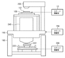
不図示の露光光源より出射された露光光は、照明光学系200により、レチクルステージ100に設置されたレチクル101を照射される。レチクル101を透過した光は、投影光学系240を透過して、ウエハーステージ220に設置されたウエハ222に到達する。これにより、レチクル101上に描かれた微細なパターンがウエハ222上の各チップに焼き付けられる。露光光源としては、例えば、KrFレーザ光源や、更なる微細化のために波長の短いArFレーザ光源が用いることが望ましい。
Exposure light emitted from an exposure light source (not shown) is applied to the
スキャニングステッパー(走査型露光装置)では、レチクルステージ100とウエハーステージ220はステージ制御部10、230により同期して制御される。同期走査中に露光が行われ、露光が終了すると次のチップの露光のためにウエハーステージ220がステップ駆動される。走査型露光装置では、レチクルステージ100及びウエハーステージ220の各々は、より速い加速度により加速され、より速い速度で同期走査露光される。一般に、縮小露光が行われる。通常、レチクル101対ウエハ222の露光縮小率は4:1で、レチクルステージ100とウエハーステージ220の加速度及び速度の比率は、同様に4:1である。各ステージの加速度及び速度は益々増加している。ウエハーステージ220の加速度は1G〜1.5G、速度は300mm/s〜600mm/s程度まで引き上げられている。ウエハーステージ220は、床又はベースフレーム180上に設置される。投影光学系240は床からの振動やウエハーステージ220の駆動による振動の影響を除去するためマウント160に締結される。マウント160はマウント制御部150により、ベースフレーム180から伝わる振動をキャンセルするようアクチュエータによりアクティブに制御される。
In the scanning stepper (scanning exposure apparatus), the
レチクルステージ100及びウエハーステージ220は生産性向上のために極めて高速に駆動されかつ微細化露光のために極めて精密に位置又は速度が制御されなければならない。
The
一般にこれらのステージは、エアー又は磁力等により浮上する。そして、ローレンツ力の原理を用いたリニアモータや平面モータ等のアクチュエータにより同期走査又はステップ駆動が行われる。各ステージの位置は、微細化露光のためnmオーダで精密に制御する必要がある。一般的には、不図示のレーザ干渉計により各ステージの位置が正確に監視され、ステージ制御部10、230によりフィードバック制御されている。
Generally, these stages are levitated by air or magnetic force. Then, synchronous scanning or step driving is performed by an actuator such as a linear motor or a planar motor using the principle of Lorentz force. The position of each stage needs to be precisely controlled on the order of nm for fine exposure. In general, the position of each stage is accurately monitored by a laser interferometer (not shown), and feedback control is performed by the
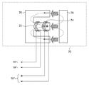
図2にリニアモータによるレチクルステージ100の構成例を示す。同期走査方向をY軸、直交する他の平面軸をX軸とする。レチクルステージ100は粗動ステージ102と微動ステージ104により構成される。粗動ステージ102には可動子110、112が取り付けられている。可動子110、112には、上下方向に磁界が発生するよう上下に磁石が取り付けられている。固定子114、118には複数のコイル群116、120が取り付けられている。これらコイル群116、120のうち、上下方向の磁界中にあるコイルに電流を流すことによりコイル電流と磁界に対して直交方向にローレンツ力が発生する。このローレンツ力が推力となって粗動ステージを駆動する。一般に、このような構成によるアクチュエータはリニアモータと呼ばれる。リニアモータは、コイル電流に対して得られる推力の線形性がよい。リニアモータの主な発熱個所はコイル群116、120である。極めて高速な加減速により大きな発熱となる。従って、コイル群116、120は、微動ステージ104から離れて配置される。不図示の冷却機構により各発熱の熱回収が行われ、微動ステージ104上に保持されたレチクル101(不図示)への影響が無いよう設計される。また、nmオーダの精密な位置制御は微動ステージ104で行われる。従って、粗動ステージ102の位置制御は微動ステージ104の制御に比べて低精度の制御でよい。
FIG. 2 shows a configuration example of a
図3に微動ステージ104を制御するためのアクチュエータ構成の一例を示す。
FIG. 3 shows an example of an actuator configuration for controlling
122、124は図2の粗動ステージに取り付けられているリニアモータと同様に不図示の磁石とコイルにより構成され、Y方向の推力を発生する。同様に126、128はX方向の推力を発生するリニアモータである。 Similar to the linear motor attached to the coarse movement stage of FIG. 2, 122 and 124 are configured by magnets and coils (not shown), and generate thrust in the Y direction. Similarly, 126 and 128 are linear motors that generate thrust in the X direction.
電磁石70y1は、磁性体によるEコア76y1とIコア78y1で構成される。このような磁性体としては、例えば、例えば、鉄等の強磁性体を用いることがより望ましい。電磁石70y1は、後述する電磁石の動作原理によりEコアとIコアと間に吸引力が発生し、微動ステージ104に対し、図示した方向の推力を与える。
The electromagnet 70y1 includes an E core 76y1 and an I core 78y1 made of a magnetic material. As such a magnetic material, for example, it is more desirable to use a ferromagnetic material such as iron. The electromagnet 70y1 generates an attractive force between the E core and the I core according to the operation principle of the electromagnet described later, and applies a thrust in the direction shown to the
同様に、電磁石70y2はEコア76y2とIコア78y2により構成される。電磁石70y2は、微動ステージ104に対し、図示した方向の推力を与える。
Similarly, the electromagnet 70y2 includes an E core 76y2 and an I core 78y2. The electromagnet 70y2 applies a thrust in the direction shown to the
EコアとIコアと間のギャップは数十〜数百μm程度で、僅かな電流により大推力が得られる。微動ステージ104は、電磁石70y1、70y2により極めて低発熱でY軸方向に大推力が印加される。
The gap between the E core and the I core is about several tens to several hundreds μm, and a large thrust can be obtained with a small current.
X、Y方向のnmオーダーの精密な位置制御はリニアモータ122、124、126、128により行われる。電磁石70y1、70y2により加減速に必要な推力は印加されている。そのため、リニアモータ122、124、126、128はnmオーダーの位置制御に必要な僅かなコイル電流により低発熱で精密な位置制御が可能となる。
Precise position control in the order of nm in the X and Y directions is performed by
図4にステージ制御部10の微動ステージ104の制御の一例を示す。
FIG. 4 shows an example of control of
微動ステージ104はレーザ干渉計等の位置計測器11により位置情報が測定される。測定された位置情報は、加減算器12に印加されて、微動ステージ104の目標値である目標位置情報との偏差が取られる。この偏差信号は、制御部14に入力され、PID制御演算等が行われてリニアモータ122、124を駆動する。以上により、微動ステージ104の精密な制御を行う。一方、目標値は、演算部18に入力され、演算部18で微動ステージ104の駆動に必要な推力Fyが算出される。ここでFyは、
Fy = m・α … 式(5)
で表される。mは微動ステージ104の質量(kg)、αは加速度(m/s2)である。推力Fyは、既知の質量と目標位置情報の2回微分との積により算出することができる。
The position information of the
Fy = m · α Equation (5)
It is represented by m is the mass (kg) of
演算部18の出力は後述する電磁石制御部20に入力され、電磁石制御部20により電磁石70y1、70y2が駆動される。これにより、低発熱かつ大推力で微動ステージ104が駆動される。
The output of the
図5に電磁石70の構成の一例を示す。
FIG. 5 shows an example of the configuration of the
駆動コイル72はEコア76に巻き付けられている。駆動コイル72に電流を流すことによりEコア76とIコア78に破線で示すような磁束が発生する。Eコア76とIコア78の対向する面にはそれぞれ磁極が発生し、磁力による吸引力が発生する。Eコア76には更に検出コイル74が巻き付けられている。この検出コイル74により駆動コイル72によって発生している磁束変化が検出される。
The
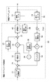
次に図6に電磁石制御部20による電磁石70の制御の構成の一例を示す。
Next, FIG. 6 shows an example of a configuration for controlling the
制御部26は、比例ゲイン又はPID等の制御演算部であり、制御部26の出力信号をVaとする。信号増幅部30は信号Vaを増幅し、信号増幅部30のゲインをGxとする。発振部34は一定振幅で所定の周波数を有する信号(変調信号)を発生する。この信号は矩形波や正弦波であること望ましい。ここでは、説明を簡単にするため振幅=1、角周波数ωの正弦波とするが、これに限定されない。変調部としての乗算器28は、制御部26の出力信号Vaと発振部34からの信号とを掛け合わせる。加算器32は信号増幅部30からの信号と乗算器28からの信号を加算し、駆動部40に印加する。従って、
駆動部40の入力 = Va(Gx+sinωt) … 式(6)
となる。
The
Input of driving
It becomes.
検出コイル74は、駆動コイル72により発生するにおける磁束変化を検出するため、定常信号では出力はゼロになる。しかしながら、本実施形態では、制御部26の出力信号Vaと発振部34からの信号とを掛け合わせることによって、検出コイル72からの信号を得ることが出来る。検出コイル72は微分動作であるため、出力振幅は周波数が高いほど大きくなり、信号検出により好適である。
Since the
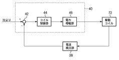
ここで図7により駆動部40の説明を行う。駆動コイル72には電力増幅部46からの信号によりコイル電流が流れる。このコイル電流を電流検出部38により検出する。電流検出部38は例えば抵抗と必要に応じて信号増幅器により構成され、コイル電流を電圧に変換して出力する。電流検出部38からの信号は加減算器42に入力され、加算器32からの出力信号との偏差が取られ、コイル制御部44に入力される。コイル制御部44では比例ゲイン又はPID等の制御演算が行われ、駆動コイル72を駆動するために必要な電圧及び電流を供給する電力増幅部46に入力される。このコイル電流のフィードバック制御によりコイル電流を加算器32の出力信号に相関した値に制御することが可能となる。コイル電流値をIcc、駆動部40における等価ゲインをGccとすると、
Icc = Va・Gcc(Gx+sinωt) … 式(7)
となる。式(4)より式(8)が得られる。
Here, the
Icc = Va · Gcc (Gx + sinωt) (7)
It becomes. Equation (8) is obtained from Equation (4).
φ ∝ Icc = Va・Gcc(Gx+sinωt) … 式(8)
また、推力Fは式(9)で表される。
φ I Icc = Va · Gcc (Gx + sin ωt) (8)
Moreover, the thrust F is represented by Formula (9).
F ∝ S・φ2 … 式(9)
検出コイル74では電磁石70内で発生している磁束変化を検出する。検出コイル74の出力信号をVnとすると、式(8)を微分して、
Vn = ω・Va・Gcc・cosωt …式(10)
が得られる。例えば、発振部34の発振周波数fを20kHzとすると、
ω=2・π・f=2・π・20*103 …式(11)
となる。これにより、発振周波数fが高いほど、より大きな出力信号が得られることが分かる。
F ∝ S · φ 2 Formula (9)
The
Vn = ω · Va · Gcc · cosωt (10)
Is obtained. For example, when the oscillation frequency f of the
ω = 2 · π · f = 2 · π · 20 * 10 3 (11)
It becomes. Thus, it can be seen that a larger output signal can be obtained as the oscillation frequency f is higher.
一方、式(8)において、信号増幅部30からの出力信号Va・Gxによって電磁石70内に発生している磁束成分φvaは、式(12)で表される。
φva ∝ Va・Gcc・Gx …式(12)
検出コイル74からの検出信号は、磁束変化が遅い場合は小さくなる。従って、出力信号Vaが直流の場合では、検出コイルの出力信号は式(10)によりVa・Gcc・Gxの成分がゼロとなる。
On the other hand, in Equation (8), the magnetic flux component φva generated in the
φva ∝ Va · Gcc · Gx (12)
The detection signal from the
次に検出コイル74の出力及び信号増幅部50の入力に外乱としてオフセット電圧Vosが重畳していると仮定する。信号増幅部50のゲインをGaとすると、信号増幅部50の出力信号は、
Vn = Ga(ω・Va・Gcc・cosωt+Vos) …式(13)
で表される。検出コイル74からの信号は、発振信号に対し微分されているため位相が90度異なる。そのため、位相調整部36により、発振部34からの信号の位相を式(13)で表される信号増幅部50からの信号の位相と同期又は180度の位相差となるよう調整する。この位相調整された位相調整部36からの信号と信号増幅部50からの信号を復調部としての乗算器52で乗算する。乗算器52からの出力信号をVmとすると、以下の式(14)で表される。
Vm = Ga(ω・Va・Gcc・cosωt+Vos)・cosωt
=1/2・Ga・ω・Va・Gcc(1+cos2ωt)+Ga・Vos・cosωt …式(14)
フィルタ54により式(14)におけるcosωtやcos2ωtの周波数成分を十分減衰させるローパスフィルタを構成し、その出力をVfbとすると、式(15)となる。
Vfb =1/2・Ga・ω・Va・Gcc …式(15)
式(15)により得られた信号は、式(12)で表される信号増幅部30からの出力信号Va・Gcc・Gxによって電磁石70内に発生している磁束成分φvaに対し、以下の式(16)の関係が成り立つ。
φva ∝ Vfb …式(16)
このように、乗算器28による変調、検出コイル74の検出信号の微分効果による信号増幅、乗算器52による復調、フィルタ54による高周波数帯域の除去を行う。これによって、外乱Vosの影響を除去し、制御部26の出力信号Vaにより電磁石70内に発生している磁束の大きさに相関した信号を正確に検出することができる。
Next, it is assumed that the offset voltage Vos is superimposed on the output of the
Vn = Ga (ω · Va · Gcc · cosωt + Vos) (13)
It is represented by Since the signal from the
Vm = Ga (ω · Va · Gcc · cosωt + Vos) · cosωt
= 1/2 · Ga · ω · Va · Gcc (1 + cos 2ωt) + Ga · Vos · cosωt (14)
If the
Vfb = 1/2 · Ga · ω · Va · Gcc (15)
The signal obtained by the equation (15) is expressed by the following equation with respect to the magnetic flux component φva generated in the
φva ∝ Vfb (16)
In this way, modulation by the
フィルタ54の出力信号は、加減算器24に入力され、スケール変換部22からの信号との偏差が取られる。この偏差信号は、制御部26に入力され、電磁石70内に発生する磁束がスケール変換部22の出力信号と等しくなるようにコイル電流が制御される。
The output signal of the
式(16)により、フィルタ54からの出力信号は、磁束に比例した信号である。そのため、推力と磁束の式(2)より、必要な推力を得るための目標磁束は、推力値の平方根で表される。従って、スケール変換部22への入力を推力目標値とすると、スケール変換部22では平方根演算が施される。
According to Expression (16), the output signal from the
EコアとIコアと間のギャップが変動すると、電磁石70内に発生する磁束の大きさが変化する。その結果、式(1)により磁束の自乗に比例して推力が大きく変動してしまう。しかしながら、上述の電磁石の制御を行うことにより、電磁石70内に発生している磁束成分が検出されてフィードバック制御が行われる。これにより、ギャップ変動によらずに目標とする磁束に制御されて、目標推力を得ることができる。
When the gap between the E core and the I core changes, the magnitude of the magnetic flux generated in the
このように、本発明の好適な実施の形態では、外乱の影響を排除し、電磁石内に発生している磁束の大きさに相関した信号を正確に検出してフィードバック制御する。これにより、電磁石におけるギャップ変動の影響を抑制し、目標とする推力を得ることができ、高速、高精度、高効率かつ低発熱でステージ制御を行うことができる。
(第2の実施形態)
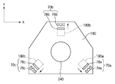
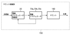
次に、図8に基づいて本発明の好適な第2の実施形態について説明する。尚、第1の実施形態と同様の動作を行う構成要素には同一符号を付し、動作に関する説明を省略する。図8は投影光学系240を支持し、床からの振動やウエハーステージ220の駆動による振動の影響を除去するマウント160の概略構成図である。電磁石70a、70b、70cは、Eコア76a、76b、76cとIコア78a、78b、78cをそれぞれ含む。マウント160にはEコア76a、76b、76cが取り付けられ、ベースフレームの柱180a、180b、180cには、Iコア78a、78b、78cが取り付けられている。3つの電磁石70a、70b、70cは図中の矢印の方向に吸引力を発生し、マウント160のXY方向の位置を制御する。
As described above, in the preferred embodiment of the present invention, the influence of disturbance is eliminated, and a signal correlated with the magnitude of the magnetic flux generated in the electromagnet is accurately detected and feedback controlled. Thereby, the influence of the gap fluctuation in the electromagnet can be suppressed, the target thrust can be obtained, and the stage control can be performed with high speed, high accuracy, high efficiency and low heat generation.
(Second Embodiment)
Next, a preferred second embodiment of the present invention will be described with reference to FIG. In addition, the same code | symbol is attached | subjected to the component which performs the operation | movement similar to 1st Embodiment, and the description regarding operation | movement is abbreviate | omitted. FIG. 8 is a schematic configuration diagram of the
図9にマウント制御部150によるマウント160の制御の一例を示す。電磁石制御部20には、床からの振動による加速度又はウエハーステージ220の駆動により発生する振動による加速度を検出する不図示のX、Y方向の加速度センサからの出力が印加される。また、電磁石制御部20には、ウエハーステージ220の駆動により予め計算されるか又は予測されるマウント160のX、Y方向の加振力をキャンセルするために必要な推力が目標値として印加されてもよい。電磁石制御部20は、第1の実施形態と同様の動作によりマウント160とベースフレーム180の柱に取り付けられた電磁石70a、70b、70cを駆動する。電磁石制御部20は、マウント160に印加される床振動やウエハーステージ220の駆動により発生する振動による外乱力をキャンセルする推力を正確に発生し振動を抑制する。
FIG. 9 shows an example of control of the
本発明の好適な実施の形態によれば、外乱の影響を排除し、電磁石内に発生している磁束の大きさに相関した信号を正確に検出してフィードバック制御することにより電磁石におけるギャップ変動の影響を抑制し、目標とする推力を得ることができる。これにより、高速、高精度、高効率かつ低発熱で除振又は制振制御を行うことが可能となる。
(応用例)
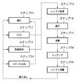
次に、上述の露光装置を利用した半導体デバイスの製造プロセスを説明する。図10は半導体デバイスの全体的な製造プロセスのフローを示す図である。ステップ1(回路設計)では半導体デバイスの回路設計を行う。ステップ2(マスク作製)では設計した回路パターンに基づいてマスクを作製する。
According to a preferred embodiment of the present invention, the influence of disturbance is eliminated, and a signal correlated with the magnitude of the magnetic flux generated in the electromagnet is accurately detected and feedback-controlled to thereby control the gap fluctuation in the electromagnet. The influence can be suppressed and the target thrust can be obtained. This makes it possible to perform vibration isolation or vibration suppression control at high speed, high accuracy, high efficiency, and low heat generation.
(Application examples)
Next, a semiconductor device manufacturing process using the above exposure apparatus will be described. FIG. 10 is a diagram showing a flow of an entire manufacturing process of a semiconductor device. In step 1 (circuit design), a semiconductor device circuit is designed. In step 2 (mask fabrication), a mask is fabricated based on the designed circuit pattern.
一方、ステップ3(ウエハ製造)ではシリコン等の材料を用いてウエハを製造する。ステップ4(ウエハプロセス)は前工程と呼ばれ、上記のマスクとウエハを用いて、上記の露光装置によりリソグラフィ技術を利用してウエハ上に実際の回路を形成する。次のステップ5(組み立て)は後工程と呼ばれ、ステップ4によって作製されたウエハを用いて半導体チップ化する工程であり、アッセンブリ工程(ダイシング、ボンディング)、パッケージング工程(チップ封入)等の組み立て工程を含む。ステップ6(検査)ではステップ5で作製された半導体デバイスの動作確認テスト、耐久性テスト等の検査を行う。こうした工程を経て半導体デバイスが完成し、ステップ7でこれを出荷する。 On the other hand, in step 3 (wafer manufacture), a wafer is manufactured using a material such as silicon. Step 4 (wafer process) is called a pre-process, and an actual circuit is formed on the wafer by using the above-described exposure apparatus and lithography technology using the above-described mask and wafer. The next step 5 (assembly) is called a post-process, and is a process for forming a semiconductor chip using the wafer produced in step 4, and is an assembly process (dicing, bonding), packaging process (chip encapsulation), etc. Process. In step 6 (inspection), the semiconductor device manufactured in step 5 undergoes inspections such as an operation confirmation test and a durability test. A semiconductor device is completed through these processes, and is shipped in Step 7.
上記ステップ4のウエハプロセスは以下のステップを有する(図11)。まず、ウエハの表面を酸化させる酸化ステップが行われる。次いで、ウエハ表面に絶縁膜を成膜するCVDステップが行われる。次いで、ウエハ上に電極を蒸着によって形成する電極形成ステップが行われる。次いで、ウエハにイオンを打ち込むイオン打ち込みステップ、ウエハに感光剤を塗布するレジスト処理ステップを行う。次いで、上記の露光装置によってレジスト処理ステップ後のウエハに回路パターンの潜像パターンを形成する露光ステップを行う。次いで、露光ステップでウエハに形成された潜像パターンを現像する現像ステップを行う。次いで、現像ステップで現像したレジスト像以外の部分を削り取るエッチングステップを行う。次いで、エッチングが済んで不要となったレジストを取り除くレジスト剥離ステップを行う。以上のように、これらのステップを繰り返し行うことによって、ウエハ上に多重に回路パターンを形成する。 The wafer process in step 4 has the following steps (FIG. 11). First, an oxidation step for oxidizing the surface of the wafer is performed. Next, a CVD step for forming an insulating film on the wafer surface is performed. Next, an electrode forming step for forming electrodes on the wafer by vapor deposition is performed. Next, an ion implantation step for implanting ions into the wafer and a resist processing step for applying a photosensitive agent to the wafer are performed. Next, an exposure step of forming a latent image pattern of a circuit pattern on the wafer after the resist processing step is performed by the above exposure apparatus. Next, a development step for developing the latent image pattern formed on the wafer in the exposure step is performed. Next, an etching step is performed to remove portions other than the resist image developed in the development step. Next, a resist stripping step is performed to remove the resist that has become unnecessary after etching. As described above, by repeating these steps, multiple circuit patterns are formed on the wafer.
Claims (12)
前記電磁アクチュエータをフィードバック制御する電磁アクチュエータ制御部と、
を備え、
前記電磁アクチュエータ制御部は、
前記第1のコイルに変調信号を与える変調部と、
前記第2のコイルからの出力信号を復調する復調部と、
を有することを特徴とする駆動装置。 An electromagnetic actuator having a first coil and a second coil for detecting a magnetic flux change generated by the first coil;
An electromagnetic actuator controller for feedback controlling the electromagnetic actuator;
With
The electromagnetic actuator controller is
A modulation unit for applying a modulation signal to the first coil;
A demodulator that demodulates an output signal from the second coil;
A drive device comprising:
前記電磁アクチュエータ制御部は、前記目標値に平方根演算を施すスケール変換部を有し、該スケール変換部からの出力信号と前記復調部で復調された信号とに基づいて前記電磁アクチュエータをフィードバック制御することを特徴とする請求項2又は請求項3に記載の駆動装置。 The target value is generated based on a force generated by the electromagnetic actuator,
The electromagnetic actuator control unit includes a scale conversion unit that performs a square root operation on the target value, and feedback-controls the electromagnetic actuator based on an output signal from the scale conversion unit and a signal demodulated by the demodulation unit. The drive device according to claim 2 or claim 3, wherein
前記第1のコイルに流れる電流を検出する電流検出部と、
前記第1のコイルに流れる電流をフィードバック制御するコイル制御部と、
を備えることを特徴とする請求項1乃至請求項6のいずれか1項に記載の駆動装置。 A power amplifying unit for driving the first coil;
A current detection unit for detecting a current flowing in the first coil;
A coil control unit that feedback-controls the current flowing through the first coil;
The drive device according to any one of claims 1 to 6, further comprising:
前記第1、第2のコイルは、前記Eコアにそれぞれ取り付けられることを特徴とする請求項1乃至請求項7のいずれか1項に記載の駆動装置。 The electromagnetic actuator has an E core and an I core,
The driving device according to claim 1, wherein the first and second coils are respectively attached to the E core.
請求項1乃至請求項8のいずれか1項に記載の駆動装置によって、前記粗動ステージに対して前記微動ステージが駆動されることを特徴とするステージ装置。 A stage device comprising a coarse movement stage and a fine movement stage,
9. A stage apparatus, wherein the fine movement stage is driven with respect to the coarse movement stage by the driving apparatus according to claim 1.
パターンを形成した原版に照射される露光光を基板に投影するための光学系と、
前記基板または前記原版を保持し前記駆動装置により位置決めされるステージ装置と、
を備えることを特徴とする露光装置。 The drive device according to any one of claims 1 to 8,
An optical system for projecting the exposure light applied to the pattern-formed original plate onto the substrate;
A stage device that holds the substrate or the original plate and is positioned by the driving device;
An exposure apparatus comprising:
請求項1乃至請求項8のいずれか1項に記載の駆動装置によって、投影光学系を支持するためのマウントを駆動することを特徴とする露光装置。 An exposure apparatus,
An exposure apparatus for driving a mount for supporting a projection optical system by the driving apparatus according to claim 1.
請求項10又は請求項11に記載の露光装置を用いて潜像パターンが形成された基板を用意する工程と、
前記潜像パターンを現像する工程と、
を含むことを特徴とするデバイス製造方法。 A device manufacturing method comprising:
Preparing a substrate on which a latent image pattern is formed using the exposure apparatus according to claim 10 or 11,
Developing the latent image pattern;
A device manufacturing method comprising:
Priority Applications (2)
| Application Number | Priority Date | Filing Date | Title |
|---|---|---|---|
| JP2005206126A JP2007027331A (en) | 2005-07-14 | 2005-07-14 | Driving device, exposure device using the same and device manufacturing method |
| US11/485,360 US7602086B2 (en) | 2005-07-14 | 2006-07-13 | Driving device, exposure apparatus using the same, and device manufacturing method |
Applications Claiming Priority (1)
| Application Number | Priority Date | Filing Date | Title |
|---|---|---|---|
| JP2005206126A JP2007027331A (en) | 2005-07-14 | 2005-07-14 | Driving device, exposure device using the same and device manufacturing method |
Publications (2)
| Publication Number | Publication Date |
|---|---|
| JP2007027331A true JP2007027331A (en) | 2007-02-01 |
| JP2007027331A5 JP2007027331A5 (en) | 2008-08-28 |
Family
ID=37661363
Family Applications (1)
| Application Number | Title | Priority Date | Filing Date |
|---|---|---|---|
| JP2005206126A Withdrawn JP2007027331A (en) | 2005-07-14 | 2005-07-14 | Driving device, exposure device using the same and device manufacturing method |
Country Status (2)
| Country | Link |
|---|---|
| US (1) | US7602086B2 (en) |
| JP (1) | JP2007027331A (en) |
Cited By (6)
| Publication number | Priority date | Publication date | Assignee | Title |
|---|---|---|---|---|
| JP2012019213A (en) * | 2010-07-09 | 2012-01-26 | Asml Netherlands Bv | Variable reluctance device, stage apparatus, lithographic apparatus and device manufacturing method |
| JP2012235026A (en) * | 2011-05-06 | 2012-11-29 | Canon Inc | Positioning apparatus, exposure apparatus and device manufacturing method |
| JP2014192254A (en) * | 2013-03-26 | 2014-10-06 | Canon Inc | Stage apparatus, lithography apparatus, and device manufacturing method |
| JP2016502124A (en) * | 2012-10-15 | 2016-01-21 | エーエスエムエル ネザーランズ ビー.ブイ. | Actuating mechanism, optical apparatus, lithographic apparatus, and device manufacturing method |
| JPWO2018181912A1 (en) * | 2017-03-31 | 2020-02-13 | 株式会社ニコン | Moving object apparatus, exposure apparatus, flat panel display manufacturing method, device manufacturing method, and moving object driving method |
| US11349273B2 (en) | 2018-01-17 | 2022-05-31 | Cymer, Llc | Apparatus for tuning discharge performance in a laser chamber |
Families Citing this family (10)
| Publication number | Priority date | Publication date | Assignee | Title |
|---|---|---|---|---|
| JP4366386B2 (en) | 2006-09-07 | 2009-11-18 | キヤノン株式会社 | Exposure apparatus and device manufacturing method |
| US7579793B2 (en) * | 2007-02-14 | 2009-08-25 | Honeywell International Inc. | System and method for efficient wide dynamic range coil drive |
| US20080285005A1 (en) * | 2007-05-15 | 2008-11-20 | Jean-Marc Gery | System and method for measuring and mapping a sideforce for a mover |
| JP2009094163A (en) * | 2007-10-04 | 2009-04-30 | Canon Inc | Temperature regulating apparatus, exposure apparatus, and device manufacturing method |
| JP5180555B2 (en) * | 2007-10-04 | 2013-04-10 | キヤノン株式会社 | Positioning apparatus, exposure apparatus, and device manufacturing method |
| EP2492928A3 (en) * | 2011-02-22 | 2017-08-30 | ASML Netherlands BV | Electromagnetic actuator, stage apparatus and lithographic apparatus |
| EP2515168B1 (en) * | 2011-03-23 | 2021-01-20 | ASML Netherlands B.V. | Methods and apparatus for calculating electromagnetic scattering properties of a structure and for reconstruction of approximate structures |
| JP2015536125A (en) * | 2012-09-19 | 2015-12-17 | エーエスエムエル ネザーランズ ビー.ブイ. | Method for calibrating a reluctance actuator assembly, reluctance actuator, and lithographic apparatus comprising a reluctance actuator |
| NL2010611C2 (en) * | 2013-04-10 | 2014-10-13 | Univ Delft Tech | Magnetic actuator and method of controlling such a magnetic actuator. |
| WO2015163886A1 (en) * | 2014-04-24 | 2015-10-29 | Empire Technology Development, Llc | Broadcasting a message using modulated power |
Family Cites Families (9)
| Publication number | Priority date | Publication date | Assignee | Title |
|---|---|---|---|---|
| US3689885A (en) * | 1970-09-15 | 1972-09-05 | Transitag Corp | Inductively coupled passive responder and interrogator unit having multidimension electromagnetic field capabilities |
| US4463354A (en) * | 1981-12-09 | 1984-07-31 | Sears Lawrence M | Apparatus for communicating utility usage related information from a utility usage location to a portable utility usage registering device |
| GB8627241D0 (en) * | 1986-11-14 | 1986-12-17 | Chubb Lips Nederland Bv | Identification token |
| US4922200A (en) * | 1989-08-25 | 1990-05-01 | Ldj Electronics, Inc. | Apparatus for measuring the hysteresis loop of magnetic film |
| US5008664A (en) * | 1990-01-23 | 1991-04-16 | Quantum Solutions, Inc. | Apparatus for inductively coupling signals between a downhole sensor and the surface |
| NL9100407A (en) | 1991-03-07 | 1992-10-01 | Philips Nv | OPTICAL LITHOGRAPHIC DEVICE WITH A FORCE COMPENSATED MACHINE FRAME. |
| JP2728018B2 (en) * | 1995-04-18 | 1998-03-18 | 日本電気株式会社 | Transmission circuit |
| US6486941B1 (en) * | 2000-04-24 | 2002-11-26 | Nikon Corporation | Guideless stage |
| JP2002280801A (en) * | 2001-03-16 | 2002-09-27 | Mitsubishi Electric Corp | Antenna system and waveguide rotary coupler |
-
2005
- 2005-07-14 JP JP2005206126A patent/JP2007027331A/en not_active Withdrawn
-
2006
- 2006-07-13 US US11/485,360 patent/US7602086B2/en not_active Expired - Fee Related
Cited By (9)
| Publication number | Priority date | Publication date | Assignee | Title |
|---|---|---|---|---|
| JP2012019213A (en) * | 2010-07-09 | 2012-01-26 | Asml Netherlands Bv | Variable reluctance device, stage apparatus, lithographic apparatus and device manufacturing method |
| US9081307B2 (en) | 2010-07-09 | 2015-07-14 | Asml Netherlands B.V. | Variable reluctance device, stage apparatus, lithographic apparatus and device manufacturing method |
| JP2012235026A (en) * | 2011-05-06 | 2012-11-29 | Canon Inc | Positioning apparatus, exposure apparatus and device manufacturing method |
| JP2016502124A (en) * | 2012-10-15 | 2016-01-21 | エーエスエムエル ネザーランズ ビー.ブイ. | Actuating mechanism, optical apparatus, lithographic apparatus, and device manufacturing method |
| JP2014192254A (en) * | 2013-03-26 | 2014-10-06 | Canon Inc | Stage apparatus, lithography apparatus, and device manufacturing method |
| US10036965B2 (en) | 2013-03-26 | 2018-07-31 | Canon Kabushiki Kaisha | Stage apparatus, lithography apparatus, and device manufacturing method |
| JPWO2018181912A1 (en) * | 2017-03-31 | 2020-02-13 | 株式会社ニコン | Moving object apparatus, exposure apparatus, flat panel display manufacturing method, device manufacturing method, and moving object driving method |
| JP2023029356A (en) * | 2017-03-31 | 2023-03-03 | 株式会社ニコン | Movable body device, exposure apparatus, and method of producing device |
| US11349273B2 (en) | 2018-01-17 | 2022-05-31 | Cymer, Llc | Apparatus for tuning discharge performance in a laser chamber |
Also Published As
| Publication number | Publication date |
|---|---|
| US20070013895A1 (en) | 2007-01-18 |
| US7602086B2 (en) | 2009-10-13 |
Similar Documents
| Publication | Publication Date | Title |
|---|---|---|
| JP2007027331A (en) | Driving device, exposure device using the same and device manufacturing method | |
| JP5530983B2 (en) | Variable reluctance device, stage apparatus, lithographic apparatus, and device manufacturing method | |
| US7468589B2 (en) | Lithographic apparatus having a controlled motor, and motor control system and method | |
| US6720680B1 (en) | Flat motor device and its driving method, stage device and its driving method, exposure apparatus and exposure method, and device and its manufacturing method | |
| US7737419B2 (en) | Alignment apparatus, exposure apparatus, and device manufacturing method | |
| US10114296B2 (en) | Driving system and driving method, and exposure apparatus and exposure method | |
| JP2007103657A (en) | Optical element retaining device, exposure device and device manufacturing method | |
| JP4857505B2 (en) | Method and apparatus for operating a vibration isolation system having an electrical control system and a pneumatic control system | |
| JP2005046941A (en) | Stage device with cable jogging unit | |
| JPH11327657A (en) | Active vibration isolator and exposuring device | |
| JP2005147281A (en) | Vibration removal device, exposure device and device manufacturing process | |
| JP2007120646A (en) | Damping device and exposure device having the same | |
| JP2008069890A (en) | Vibration eliminating device, exposure device, and device manufacturing method | |
| JP2003249439A (en) | Stage-positioning apparatus and control method thereof, projection aligner, and manufacturing method for semiconductor device | |
| US8970821B2 (en) | Positioning apparatus, exposure apparatus and device manufacturing method | |
| JP2005303196A (en) | Positioning device, aligner, and manufacturing method of semiconductor device | |
| JP2004134456A (en) | Moving device, aligner, and method of manufacturing device | |
| US20060103833A1 (en) | Aligning apparatus and its control method, and exposure apparatus | |
| JP2009087371A (en) | Positioning device, exposure device, and device manufacturing method | |
| US20120281194A1 (en) | Positioning apparatus, exposure apparatus, and method of manufacturing device | |
| JP2014192254A (en) | Stage apparatus, lithography apparatus, and device manufacturing method | |
| JP2000068195A (en) | Device manufacturing equipment | |
| JP4541849B2 (en) | Positioning device | |
| JP2001217172A (en) | Stage device and exposure system | |
| JP2001258289A (en) | Linear motor, stage, aligner, and method for manufacturing device |
Legal Events
| Date | Code | Title | Description |
|---|---|---|---|
| A521 | Written amendment |
Free format text: JAPANESE INTERMEDIATE CODE: A523 Effective date: 20080710 |
|
| A621 | Written request for application examination |
Free format text: JAPANESE INTERMEDIATE CODE: A621 Effective date: 20080710 |
|
| A761 | Written withdrawal of application |
Free format text: JAPANESE INTERMEDIATE CODE: A761 Effective date: 20100607 |