JP2007015169A - Scribing formation method, scribing formation apparatus, and multilayer substrate - Google Patents
Scribing formation method, scribing formation apparatus, and multilayer substrate Download PDFInfo
- Publication number
- JP2007015169A JP2007015169A JP2005197394A JP2005197394A JP2007015169A JP 2007015169 A JP2007015169 A JP 2007015169A JP 2005197394 A JP2005197394 A JP 2005197394A JP 2005197394 A JP2005197394 A JP 2005197394A JP 2007015169 A JP2007015169 A JP 2007015169A
- Authority
- JP
- Japan
- Prior art keywords
- multilayer substrate
- layers
- laser
- scribe
- light transmission
- Prior art date
- Legal status (The legal status is an assumption and is not a legal conclusion. Google has not performed a legal analysis and makes no representation as to the accuracy of the status listed.)
- Pending
Links
Images


Classifications
-
- B—PERFORMING OPERATIONS; TRANSPORTING
- B23—MACHINE TOOLS; METAL-WORKING NOT OTHERWISE PROVIDED FOR
- B23K—SOLDERING OR UNSOLDERING; WELDING; CLADDING OR PLATING BY SOLDERING OR WELDING; CUTTING BY APPLYING HEAT LOCALLY, e.g. FLAME CUTTING; WORKING BY LASER BEAM
- B23K26/00—Working by laser beam, e.g. welding, cutting or boring
- B23K26/50—Working by transmitting the laser beam through or within the workpiece
- B23K26/53—Working by transmitting the laser beam through or within the workpiece for modifying or reforming the material inside the workpiece, e.g. for producing break initiation cracks
Landscapes
- Engineering & Computer Science (AREA)
- Physics & Mathematics (AREA)
- Optics & Photonics (AREA)
- Chemical & Material Sciences (AREA)
- Chemical Kinetics & Catalysis (AREA)
- General Chemical & Material Sciences (AREA)
- Oil, Petroleum & Natural Gas (AREA)
- Plasma & Fusion (AREA)
- Mechanical Engineering (AREA)
- Processing Of Stones Or Stones Resemblance Materials (AREA)
- Laser Beam Processing (AREA)
- Re-Forming, After-Treatment, Cutting And Transporting Of Glass Products (AREA)
Abstract
Description
本発明は、複数の層を積層させた多層基板に対して分割予定線を形成するスクライブ形成方法、スクライブ形成装置に関する。 The present invention relates to a scribe forming method and a scribe forming apparatus for forming a division line on a multilayer substrate in which a plurality of layers are laminated.
液晶装置等に広く使用されているガラス基板を複数に分割する方法として、基板の表面に溝(分割予定線,スクライブライン)を刻み、この溝に沿って基板を分割する方法が一般に用いられている(特許文献1等)。
特に、複数のガラス基板を積層させた多層基板を分割する場合には、各層のガラス基板のそれぞれに溝を形成した上で、各溝が一致するように各基板を重ねることで、多層基板の分割を可能としている。また、レーザとカッターを併用することで、多層基板に溝を形成する技術も提案されている(特許文献2)。
In particular, when dividing a multilayer substrate in which a plurality of glass substrates are laminated, a groove is formed in each of the glass substrates of each layer, and then the substrates are stacked so that the grooves coincide with each other. Splitting is possible. In addition, a technique for forming a groove in a multilayer substrate by using a laser and a cutter together has been proposed (Patent Document 2).
しかしながら、上述した技術では、基板に溝を形成する際に発生した切り屑が基板上に付着するため、これをクリーニング処理する工程が必要となる。そして、このクリーニング処理工程が、製造効率の低下やコスト上昇が招く原因となっている。
特に、積層される層が多くなると、切り屑の量が増えたり、或いは溝の深さが不十分となって基板の分割が困難になったりするという問題がある。
However, in the above-described technique, chips generated when grooves are formed on the substrate adhere to the substrate, and thus a process of cleaning the chip is necessary. And this cleaning process process causes a decrease in manufacturing efficiency and an increase in cost.
In particular, when the number of layers to be stacked increases, there is a problem that the amount of chips increases, or the depth of the groove becomes insufficient and it becomes difficult to divide the substrate.
本発明は、上述した事情に鑑みてなされたもので、複数の層を積層させた多層基板に対して、切り屑を発生させることなく、かつ良好に分割することが可能な分割予定線を形成することができるスクライブ形成方法、スクライブ形成装置、多層基板を提案することを目的とする。 The present invention has been made in view of the above-described circumstances, and forms a planned dividing line that can be divided satisfactorily without generating chips on a multilayer substrate in which a plurality of layers are stacked. An object of the present invention is to propose a scribe forming method, a scribe forming apparatus, and a multilayer substrate.
本発明に係るスクライブ形成方法、スクライブ形成装置、多層基板では、上記課題を解決するために以下の手段を採用した。
第1の発明は、複数の光透過層を有する多層基板に分割予定線を形成するスクライブ形成方法が、前記多層基板の内部にレーザ光を集光すると共に前記多層基板と前記レーザ光を相対移動させて、前記多層基板内に改質領域を形成する工程と、前記改質領域を前記多層基板の厚み方向に複数重ねて形成する工程と、を有するようにした。
この発明によれば、レーザ光を用いて多層基板内に分割予定線を形成するので、多層基板上に切り屑が付着せず、したがってクリーニング処理が不要となる。また、複数の光透過層のそれぞれに改質領域からなる分割予定線を形成し、更にこの分割予定線を基板の厚み方向に重ねるので、光透過層の数に関わらず、良好に多層基板を分割することが可能となる。
The scribe forming method, the scribe forming apparatus, and the multilayer substrate according to the present invention employ the following means in order to solve the above problems.
According to a first aspect of the present invention, there is provided a scribe forming method for forming a division line on a multilayer substrate having a plurality of light transmission layers, wherein the laser beam is condensed inside the multilayer substrate and the multilayer substrate and the laser beam are relatively moved. Thus, the method includes a step of forming a modified region in the multilayer substrate and a step of forming a plurality of the modified regions in the thickness direction of the multilayer substrate.
According to the present invention, the dividing lines are formed in the multilayer substrate using the laser beam, so that chips do not adhere to the multilayer substrate, and therefore no cleaning process is required. In addition, since each of the plurality of light-transmitting layers is formed with a dividing line composed of a modified region, and this dividing line is overlapped in the thickness direction of the substrate, a multilayer substrate can be satisfactorily formed regardless of the number of light-transmitting layers. It becomes possible to divide.
また、前記複数の層が光透過層であるものでは、レーザ光の損失が少なくなり、内部に良好に改質領域を形成することができる。
また、前記レーザ光として、超短パルスレーザ光を用いるものでは、焦点位置にのみ良好に改質領域を形成することができる。これにより、細い幅の分割予定線が形成されるので、基板の分割効率を向上させることができる。
Further, when the plurality of layers are light transmission layers, the loss of laser light is reduced, and a modified region can be formed favorably inside.
In addition, when an ultrashort pulse laser beam is used as the laser beam, a modified region can be formed satisfactorily only at the focal position. Thereby, since the division | segmentation planned line of a narrow width | variety is formed, the division | segmentation efficiency of a board | substrate can be improved.
第2の発明は、複数の光透過層を有する多層基板に分割予定線を形成するスクライブ形成装置が、前記多層基板を載置すると共に前記多層基板の面方向に二次元移動可能なステージと、前記多層基板に対してレーザ光を照射するレーザ投光部と、前記レーザ投光部からのレーザ光の焦点を前記多層基板の厚み方向に移動可能な焦点移動部と、を備えるようにした。
この発明によれば、レーザ光を用いて多層基板内に分割予定線を形成するので、多層
基板上に切り屑が付着せず、したがってクリーニング処理が不要となる。また、複数の光透過層のそれぞれに改質領域からなる分割予定線を形成し、更にこの分割予定線を多層基板の厚み方向に重ねることで、光透過層の数に関わらず、良好に多層基板を分割することが可能となる。
According to a second aspect of the present invention, there is provided a scribe forming apparatus for forming a division line on a multilayer substrate having a plurality of light transmission layers. The stage is configured to place the multilayer substrate and move two-dimensionally in the plane direction of the multilayer substrate; A laser projection unit that irradiates the multilayer substrate with laser light, and a focal point moving unit that can move the focal point of the laser beam from the laser projection unit in the thickness direction of the multilayer substrate.
According to the present invention, the dividing lines are formed in the multilayer substrate using the laser beam, so that chips do not adhere to the multilayer substrate, and therefore no cleaning process is required. In addition, by forming a planned dividing line consisting of a modified region in each of the plurality of light transmitting layers, and further superimposing this dividing planned line in the thickness direction of the multilayer substrate, it is possible to achieve a good multilayer regardless of the number of light transmitting layers. The substrate can be divided.
また、前記複数の層が光透過層であるものでは、レーザ光の損失が少なくなり、内部に良好に改質領域を形成することができる。
また、前記レーザ光として、超短パルスレーザ光を用いるものでは、焦点位置にのみ良好に改質領域を形成することができる。これにより、細い幅の分割予定線が形成されるので、基板の分割効率を向上させることができる。
Further, when the plurality of layers are light transmission layers, the loss of laser light is reduced, and a modified region can be formed favorably inside.
In addition, when an ultrashort pulse laser beam is used as the laser beam, a modified region can be formed satisfactorily only at the focal position. Thereby, since the division | segmentation planned line of a narrow width | variety is formed, the division | segmentation efficiency of a board | substrate can be improved.
第3の発明は、複数の光透過層から形成される多層基板が、前記光透過層のそれぞれに、改質領域を前記多層基板の厚み方向に重ねた分割予定線を有するようにした。
この発明によれば、複数の光透過層のそれぞれに改質領域からなる分割予定線が形成され、更にこの分割予定線が多層基板の厚み方向に重ねられているので、光透過層の数に関わらず、良好に多層基板を分割することができる。
According to a third aspect of the present invention, a multilayer substrate formed of a plurality of light transmission layers has a division line in which a modified region is overlapped in the thickness direction of the multilayer substrate in each of the light transmission layers.
According to the present invention, each of the plurality of light-transmitting layers is formed with a dividing line composed of a modified region, and the dividing lines are overlapped in the thickness direction of the multilayer substrate. Regardless, the multilayer substrate can be divided well.
以下、本発明のスクライブ形成方法、スクライブ形成装置、多層基板の実施形態について図を参照して説明する。
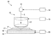
図1は、スクライブ形成装置10の概略構成を示す概念図である。
スクライブ形成装置10は、レーザ光Lを発生するレーザ光源11、レーザ光Lの出力やパルス幅等を調節するためにレーザ光源11を制御するレーザ光源制御部14、レーザ光Lを集光する集光用レンズ12、集光用レンズ12等をZ軸方向に移動させるためのZ軸駆動部15、多層基板Pを載置する載置台17、載置台17をX軸方向に移動させるためのX軸ステージ18、載置台17をX軸方向に直交するY軸方向に移動させるためのY軸ステージ19、X軸ステージ18及びY軸ステージ19を制御するステージ制御部20等を備える。
Hereinafter, embodiments of a scribe forming method, a scribe forming apparatus, and a multilayer substrate according to the present invention will be described with reference to the drawings.
FIG. 1 is a conceptual diagram showing a schematic configuration of the
The
レーザ光源11、集光用レンズ12等からなるレーザ投光部13から射出されるレーザ光Lには、超短パルスレーザが用いられる。例えば、パルス幅300fs、出力170mW、繰り返し率1kHz、波長800nm、倍率100倍(NA0.8)のフェムト秒レーザが用いられる。
フェムト秒レーザのような超短パルスレーザは、出力が小さくても、パルス幅が非常に短いため、1パルス中の瞬間的な到達出力は大きくなる。
したがって、超短パルスレーザを集光照射すると,熱伝導が起こる前に瞬時にエネルギーが注入されるため、照射部位周辺が熱的・化学的損傷をほとんど受けない高精度・高品質な加工が実現できる。そして、多光子吸収という現象を利用して、通常であれば光が通り抜けてしまうガラスやダイヤモンド等の透明材料の内部への3次元加工が可能である。
An ultrashort pulse laser is used for the laser light L emitted from the laser
Even if the output is small, an ultrashort pulse laser such as a femtosecond laser has a very short pulse width, so that an instantaneous arrival power in one pulse is large.
Therefore, when the ultra-short pulse laser is focused and irradiated, energy is injected instantaneously before heat conduction occurs, so high-precision and high-quality processing is achieved with almost no thermal or chemical damage around the irradiated area. it can. By utilizing the phenomenon of multiphoton absorption, three-dimensional processing into a transparent material such as glass or diamond that normally allows light to pass through is possible.
Z軸駆動部15は、レーザ投光部13をZ軸方向に移動させることにより、レーザ光Lの焦点をZ軸方向に移動させるものである。すなわち、Z軸方向は多層基板Pの表面Psと直交する方向であり、また集光用レンズ12等を介して多層基板Pに入射するレーザ光Lの焦点深度の方向でもある。したがって、Z軸駆動部15によりレーザ投光部13をZ軸方向に移動させることにより、多層基板Pの内部に集光したレーザ光Lの焦点を、Z軸方向に移動させることができる。
The Z-
X軸ステージ18、Y軸ステージ19は、多層基板PをX軸方向及びY軸方向に移動させることで、多層基板P内に集光したレーザ光Lの焦点を多層基板P内でX軸方向及びY軸方向に移動させることができる。
The
多層基板Pとしては、石英やソーダガラス等を重ね合わせたものが用いられる。また、これらの基板の間に透明な接着層等を含んでいてもよい。すなわち、光を透過する層が積層されることで、少なくとも一方の面から内部に向けてレーザ光Lを照射できる多層基板であればよい。 As the multilayer substrate P, a laminate of quartz, soda glass or the like is used. Further, a transparent adhesive layer or the like may be included between these substrates. That is, any multilayer substrate that can irradiate the laser beam L from at least one surface to the inside by stacking layers that transmit light may be used.
次に、本実施形態に係るスクライブ形成方法について説明する。
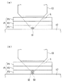
図2,図3は、スクライブ形成方法を示す図であって、図2は多層基板の断面図、図3は多層基板の平面図である。
また、図4は、分断予定線が形成された多層基板を示す断面図である。
Next, the scribe forming method according to this embodiment will be described.
2 and 3 are diagrams showing a scribe forming method, in which FIG. 2 is a cross-sectional view of the multilayer substrate, and FIG. 3 is a plan view of the multilayer substrate.
FIG. 4 is a cross-sectional view showing a multilayer substrate on which a parting line is formed.
まず、載置台17上に多層基板Pを載置する。そして、Z軸駆動部15によりレーザ投光部13をZ軸方向に移動させて、多層基板Pの最下光透過層P3内にレーザ光Lの焦点が合うように位置決めする。具体的には、最下光透過層P3の最も下層、すなわち裏面Ptに近接する位置にレーザ光Lの焦点位置を合わせる。なお、焦点位置は、多層基板Pの各光透過層P1〜P3の屈折率を予め求めておくことで、推測可能である。したがって、各光透過層P1〜P3の屈折率がそれぞれ異なる場合であってもよい。
First, the multilayer substrate P is mounted on the mounting table 17. Then, the
次いで、レーザ投光部13からフェムト秒レーザを照射して、最下光透過層P3内に改質領域を形成する(図2(a),図3(a)参照)。これと同時に、図3(b)に示すように、X軸ステージ18及びY軸ステージ19を駆動して、多層基板Pをレーザ投光部13に対して移動させる。なお、X軸ステージ18、Y軸ステージ19の走査速度としては、例えば、約20mm/sである。
Next, a femtosecond laser is irradiated from the
フェムト秒レーザを用いたスクライブ形成方法では、多層基板Pにレーザ光Lを透過させ、多層基板Pの内部に多光子吸収を発生させることで、微細なクラック等を有する改質領域を形成するものである。
すなわち、多層基板Pがレーザ光Lを吸収することにより多層基板Pを発熱・溶融させるのではない。このため、多層基板Pの焦点以外の部位、例えば表面Psではレーザ光Lがほとんど吸収されず、溶融等を発生することはない。
In the scribe formation method using a femtosecond laser, a laser beam L is transmitted through the multilayer substrate P and multiphoton absorption is generated inside the multilayer substrate P, thereby forming a modified region having fine cracks and the like. It is.
That is, the multilayer substrate P does not generate heat and melt by absorbing the laser light L. For this reason, the laser beam L is hardly absorbed at a portion other than the focal point of the multilayer substrate P, for example, the surface Ps, and melting or the like does not occur.
このようにして、図2(a),図3(b)に示すように、最下光透過層P3内にライン状の改質領域S1が多層基板Pを横断するように形成される。このライン状の改質領域S1は、周辺領域に比べて脆弱な領域であり、したがって、改質領域S1に沿って多層基板Pを複数に分割することが可能となる。 In this way, as shown in FIGS. 2A and 3B, the line-shaped modified region S1 is formed in the lowermost light transmission layer P3 so as to cross the multilayer substrate P. The line-shaped modified region S1 is a region that is more fragile than the peripheral region, and therefore, the multilayer substrate P can be divided into a plurality along the modified region S1.
ところで、多層基板Pの最下光透過層P3内に改質領域S1を形成したのみでは、多層基板Pの分割は殆ど不可能である。多層基板Pの厚みに対する改質領域S1のZ軸方向の距離(厚み)が小さいからである。
そこで、図2(b)に示すように、改質領域S1の上部(+Z方向)に、更に改質領域を重ねて形成することで、改質領域のZ軸方向の距離(厚み)を大きくする。具体的には、Z軸駆動部15によりレーザ投光部13を+Z軸方向に移動させて、レーザ光Lの焦点位置を最下光透過層P3内の中間部等に移動させる。そして、改質領域S1に沿って、改質領域S1の上部に重ねて改質領域S2を形成する(図3参照)。
By the way, the division of the multilayer substrate P is almost impossible only by forming the modified region S1 in the lowermost light transmission layer P3 of the multilayer substrate P. This is because the distance (thickness) in the Z-axis direction of the modified region S1 with respect to the thickness of the multilayer substrate P is small.
Therefore, as shown in FIG. 2B, the distance (thickness) in the Z-axis direction of the modified region is increased by forming the modified region on top of the modified region S1 (+ Z direction). To do. Specifically, the
そして、レーザ光Lの焦点位置をZ方向に移動させつつ、改質領域を重ねて形成する工程を複数回繰り返すことで、各光透過層P1〜P3のそれぞれに、ライン状の改質領域S1〜Snを形成する。
このようにして、図4に示すように、Z方向に重ねて配置された複数のライン状の改質領域S1〜Snからなる分割予定線Sを形成する。そして、分割予定線S(改質領域S1〜Sn)の多層基板Pの厚みに対するのZ軸方向の距離(厚み)は十分に大きくなっているので、容易に多層基板Pをこの分割予定線Sに沿って分割することが可能となる。
Then, by repeating the step of forming the modified region in an overlapping manner while moving the focal position of the laser beam L in the Z direction, each of the light transmission layers P1 to P3 has a linear modified region S1. ~ Sn is formed.
In this way, as shown in FIG. 4, the division planned line S composed of a plurality of line-shaped modified regions S <b> 1 to Sn arranged in the Z direction is formed. And since the distance (thickness) in the Z-axis direction with respect to the thickness of the multilayer substrate P of the division line S (modified regions S1 to Sn) is sufficiently large, the multilayer substrate P can be easily separated from the division line S. It becomes possible to divide along.
なお、多層基板Pの分割は、多層基板Pに比較的小さな力を加えること行われる。すなわち、分割予定線Sに沿って亀裂が発生、進行して、多層基板Pが分割(分断)される。また、分割予定線Sに沿って亀裂が発生するので、多層基板Pに不必要な割れを発生させることなく、良好に分割することができる。 The division of the multilayer substrate P is performed by applying a relatively small force to the multilayer substrate P. That is, a crack is generated and proceeds along the planned dividing line S, and the multilayer substrate P is divided (divided). Further, since the cracks are generated along the planned dividing line S, the multilayer substrate P can be divided satisfactorily without causing unnecessary cracks.
なお、多層基板Pに力を加える方法としては、例えば、分割予定線Sに沿って多層基板Pに曲げ応力やせん断応力を加えたり、多層基板Pに温度差を与えて熱応力を発生させたりする。 As a method for applying force to the multilayer substrate P, for example, bending stress or shear stress is applied to the multilayer substrate P along the planned dividing line S, or thermal stress is generated by applying a temperature difference to the multilayer substrate P. To do.
上述した実施形態においては、説明を分かりやすくするために、ライン(直線)状の分割予定線Sを1本だけ形成する場合について説明したが、これに限らない。複数の分割予定線を平行に形成する場合であってもよい。また、曲線状や格子状の分割予定線を形成してもよい。このような場合であっても、改質領域をZ軸方に重ねて形成する必要があることは言うまでもない。 In the embodiment described above, in order to make the explanation easy to understand, the case where only one line (straight line) -shaped division planned line S is formed has been described, but the present invention is not limited thereto. It may be a case where a plurality of division lines are formed in parallel. Moreover, you may form the curve and grid-like division | segmentation planned line. Even in such a case, it goes without saying that it is necessary to form the modified region so as to overlap the Z-axis direction.
また、改質領域S1〜Snは、必ずしもZ方向に密着させて配置する必要はない。Z方向に多少の間隔が開く場合であってもよい。
また、全ての改質領域S1〜Snをライン状に形成する必要はない。例えば、破線状の改質領域を形成してもよいし、ライン状と破線状の改質領域をZ軸方向に重ねて形成してもよい。複数の層内に、複数の改質領域を積層させて形成することで、全体として、Z軸方向に十分な厚みのある改質領域からなる分割予定線Sが形成されればよい。
Further, the modified regions S1 to Sn are not necessarily arranged in close contact with each other in the Z direction. It may be a case where a slight interval is opened in the Z direction.
Moreover, it is not necessary to form all the modified regions S1 to Sn in a line shape. For example, a modified region having a broken line shape may be formed, or a modified region having a line shape and a broken line shape may be overlapped in the Z-axis direction. By forming a plurality of modified regions in a plurality of layers by stacking them, it is only necessary to form the planned dividing line S composed of the modified regions having a sufficient thickness in the Z-axis direction as a whole.
多層基板PをX軸ステージ及びY軸ステージによりX軸方向及びY軸方向に移動させ、またレーザ投光部13をZ軸駆動部によりZ軸方向に移動させる場合について説明したが、これに限らない。
レーザ投光部13を固定して、多層基板PをX軸,Y軸およびZ軸方向に移動させてもよい。逆に、多層基板Pを固定して、レーザ投光部13をX軸,Y軸およびZ軸方向に移動させてもよい。
The case where the multilayer substrate P is moved in the X-axis direction and the Y-axis direction by the X-axis stage and the Y-axis stage and the
The
また、多層基板Pとしては、液晶装置や有機EL装置等のディスプレイ等が挙げられる。主に、多層基板Pの裏面Ptに、電子デバイスや配線パターン等が形成されたTFT基板がある。そして、このような多層基板Pに分割予定線Sを形成した場合には、分割予定線S以外の部分での割れが殆どなくなるので、多層基板Pの分割に伴う電子デバイスや配線パターンの損傷が防止される。
また、多層基板Pとしては、TFT基板等に限らず、内部にマイクロレンズを形成した透明基板であってもよい。
Examples of the multilayer substrate P include displays such as liquid crystal devices and organic EL devices. There is mainly a TFT substrate in which electronic devices, wiring patterns, and the like are formed on the back surface Pt of the multilayer substrate P. When the planned dividing line S is formed on such a multilayer substrate P, the cracks in the portions other than the planned dividing line S are almost eliminated, so that damage to the electronic device and the wiring pattern due to the division of the multilayer substrate P occurs. Is prevented.
Further, the multilayer substrate P is not limited to a TFT substrate or the like, and may be a transparent substrate in which microlenses are formed.
また、説明を分かりやすくするために、多層基板Pが3つの光透過層を有する場合について説明したが、層の数は複数であればよい。同様に、改質領域の数も複数であればよい。
なお、必ずしも全ての光透過層に改質領域を形成する必要はなく、例えば他の光透過層に比べて厚みが小さい薄膜層の場合には改質領域の形成を省略する等、適宜、改質領域の形成を調整してもよい。
Further, in order to make the explanation easy to understand, the case where the multilayer substrate P has three light transmission layers has been described, but the number of layers may be plural. Similarly, the number of modified regions may be plural.
Note that it is not always necessary to form the modified region in all the light transmissive layers. For example, in the case of a thin film layer having a thickness smaller than that of other light transmissive layers, the modified region may be omitted as appropriate. The formation of the quality region may be adjusted.
また、多層基板が光透過層のみを有する場合について説明したが、多層基板の一部に光を透過しない層があってもよい。例えば、最下光透過層P3が光を透過しない層の場合には、光透過層P2,P1にのみ改質領域を形成すればよい。また、例えば、中間光透過層P2が光を透過しない層の場合には、光透過層P3,P1にのみ改質領域を形成すればよい。この場合には、多層基板Pの表面Ps及び裏面Ptの両側から多層基板P内にレーザ光Lを投光することで分割予定線を形成することができる。 Further, although the case where the multilayer substrate has only the light transmission layer has been described, a layer that does not transmit light may be included in a part of the multilayer substrate. For example, when the lowermost light transmission layer P3 is a layer that does not transmit light, the modified region may be formed only in the light transmission layers P2 and P1. In addition, for example, when the intermediate light transmission layer P2 is a layer that does not transmit light, the modified region may be formed only in the light transmission layers P3 and P1. In this case, the planned division line can be formed by projecting the laser light L into the multilayer substrate P from both sides of the front surface Ps and the back surface Pt of the multilayer substrate P.
また、多層基板がガラス基板等の光透過層を有する場合について説明したが、レーザ光Lが透過するものであれば、半透明又は不透明な材料からなる多層基板であってもよい。 Moreover, although the case where the multilayer substrate has a light transmission layer such as a glass substrate has been described, a multilayer substrate made of a translucent or opaque material may be used as long as the laser light L is transmitted.
10…スクライブ形成装置、 11…レーザ光源、 13…レーザ投光部、
15…Z軸駆動部(焦点移動部)、 18…X軸ステージ、 19…Y軸ステージ、
L…レーザ光、 P…多層基板、 P1〜P3…光透過層、 S…分割予定線、
S1〜Sn…改質領域
DESCRIPTION OF
15 ... Z-axis drive unit (focus movement unit), 18 ... X-axis stage, 19 ... Y-axis stage,
L: Laser light, P: Multilayer substrate, P1 to P3: Light transmission layer, S: Planned dividing line,
S1 to Sn: reforming region
Claims (7)
前記多層基板の内部にレーザ光を集光すると共に前記多層基板と前記レーザ光を相対移動させて、前記多層基板内に改質領域を形成する工程と、
前記改質領域を前記多層基板の厚み方向に複数重ねて形成する工程と、
を有することを特徴とするスクライブ形成方法。 A scribe formation method for forming a division line on a multilayer substrate composed of a plurality of layers,
Condensing laser light inside the multilayer substrate and relatively moving the multilayer substrate and the laser light to form a modified region in the multilayer substrate;
Forming a plurality of the modified regions in the thickness direction of the multilayer substrate; and
A scribe forming method characterized by comprising:
前記多層基板を載置すると共に前記多層基板の面方向に二次元移動可能なステージと、
前記多層基板に対してレーザ光を照射するレーザ投光部と、
前記レーザ投光部からのレーザ光の焦点を前記多層基板の厚み方向に移動可能な焦点移動部と、
を備えることを特徴とするスクライブ形成装置。 A scribe forming apparatus for forming a division line on a multilayer substrate composed of a plurality of layers,
A stage capable of two-dimensional movement in the plane direction of the multilayer substrate while mounting the multilayer substrate;
A laser projection unit for irradiating the multilayer substrate with laser light;
A focal point moving unit capable of moving the focal point of the laser light from the laser projecting unit in the thickness direction of the multilayer substrate;
A scribe forming apparatus comprising:
前記光透過層のそれぞれに、改質領域を前記多層基板の厚み方向に重ねた分割予定線を有することを特徴とする多層基板。
A multilayer substrate formed of a plurality of light transmission layers,
Each of the light transmission layers has a division line in which a modified region is overlapped in a thickness direction of the multilayer substrate.
Priority Applications (1)
| Application Number | Priority Date | Filing Date | Title |
|---|---|---|---|
| JP2005197394A JP2007015169A (en) | 2005-07-06 | 2005-07-06 | Scribing formation method, scribing formation apparatus, and multilayer substrate |
Applications Claiming Priority (1)
| Application Number | Priority Date | Filing Date | Title |
|---|---|---|---|
| JP2005197394A JP2007015169A (en) | 2005-07-06 | 2005-07-06 | Scribing formation method, scribing formation apparatus, and multilayer substrate |
Publications (1)
| Publication Number | Publication Date |
|---|---|
| JP2007015169A true JP2007015169A (en) | 2007-01-25 |
Family
ID=37752741
Family Applications (1)
| Application Number | Title | Priority Date | Filing Date |
|---|---|---|---|
| JP2005197394A Pending JP2007015169A (en) | 2005-07-06 | 2005-07-06 | Scribing formation method, scribing formation apparatus, and multilayer substrate |
Country Status (1)
| Country | Link |
|---|---|
| JP (1) | JP2007015169A (en) |
Cited By (7)
| Publication number | Priority date | Publication date | Assignee | Title |
|---|---|---|---|---|
| JP2009023215A (en) * | 2007-07-19 | 2009-02-05 | Panasonic Electric Works Co Ltd | Dividing method of laminate |
| JP2011000754A (en) * | 2009-06-17 | 2011-01-06 | Canon Inc | Manufacturing method of microstructural body, and manufacturing method of liquid ejection head |
| JP2011011917A (en) * | 2009-06-30 | 2011-01-20 | Mitsuboshi Diamond Industrial Co Ltd | Glass substrate processing device using laser beam |
| JP2013220981A (en) * | 2012-04-18 | 2013-10-28 | Optoceramics:Kk | Method for manufacturing optical panel for spatial focusing |
| JP2016049542A (en) * | 2014-08-29 | 2016-04-11 | アイシン精機株式会社 | Laser processing method, manufacturing method of glass processing part and laser processor |
| JP2019063818A (en) * | 2017-09-29 | 2019-04-25 | 三星ダイヤモンド工業株式会社 | Manufacturing method and manufacturing system of multilayered brittle material substrate |
| JP2019102688A (en) * | 2017-12-05 | 2019-06-24 | 株式会社ディスコ | Processing method of wafer |
-
2005
- 2005-07-06 JP JP2005197394A patent/JP2007015169A/en active Pending
Cited By (7)
| Publication number | Priority date | Publication date | Assignee | Title |
|---|---|---|---|---|
| JP2009023215A (en) * | 2007-07-19 | 2009-02-05 | Panasonic Electric Works Co Ltd | Dividing method of laminate |
| JP2011000754A (en) * | 2009-06-17 | 2011-01-06 | Canon Inc | Manufacturing method of microstructural body, and manufacturing method of liquid ejection head |
| JP2011011917A (en) * | 2009-06-30 | 2011-01-20 | Mitsuboshi Diamond Industrial Co Ltd | Glass substrate processing device using laser beam |
| JP2013220981A (en) * | 2012-04-18 | 2013-10-28 | Optoceramics:Kk | Method for manufacturing optical panel for spatial focusing |
| JP2016049542A (en) * | 2014-08-29 | 2016-04-11 | アイシン精機株式会社 | Laser processing method, manufacturing method of glass processing part and laser processor |
| JP2019063818A (en) * | 2017-09-29 | 2019-04-25 | 三星ダイヤモンド工業株式会社 | Manufacturing method and manufacturing system of multilayered brittle material substrate |
| JP2019102688A (en) * | 2017-12-05 | 2019-06-24 | 株式会社ディスコ | Processing method of wafer |
Similar Documents
| Publication | Publication Date | Title |
|---|---|---|
| JP7449995B2 (en) | How to divide composite materials | |
| JP6585050B2 (en) | Cutting stack transparent materials using ultrafast laser beam optics, destructive layers and other layers | |
| JP4198123B2 (en) | Laser processing method | |
| KR100825884B1 (en) | Laser processing apparatus and laser processing method | |
| JP4907984B2 (en) | Laser processing method and semiconductor chip | |
| JP4776994B2 (en) | Processing object cutting method | |
| TWI380867B (en) | Laser processing methods and semiconductor wafers | |
| JP4752488B2 (en) | Laser internal scribing method | |
| WO2006051861A1 (en) | Laser processing method | |
| JP2017502901A5 (en) | ||
| JP2007260773A (en) | Substrate cutting method and substrate cutting apparatus using this method | |
| WO2011071886A1 (en) | Laser machining and scribing systems and methods | |
| JP2009023215A (en) | Dividing method of laminate | |
| JP2007015169A (en) | Scribing formation method, scribing formation apparatus, and multilayer substrate | |
| JP2009539610A (en) | Fabrication of microfluidic devices using laser-induced shock waves | |
| JP2007021514A (en) | Scribe forming method, and substrate with division projected line | |
| JP2007118009A (en) | Method for machining laminated body | |
| JP2010110818A (en) | Workpiece splitting method and object producing method | |
| JP2009242185A (en) | Laser cutting method, and object to be cut | |
| JP2007014975A (en) | Scribe forming method, and substrate with division projected line | |
| WO2021009961A1 (en) | Method for dividing composite material | |
| KR100862522B1 (en) | Laser beam machining system and method for cutting of substrate using the same | |
| JP7456604B2 (en) | Scribing method and scribing device | |
| WO2021009960A1 (en) | Method for dividing composite material | |
| JPWO2019131525A1 (en) | Scribe processing method and scribe processing equipment |
Legal Events
| Date | Code | Title | Description |
|---|---|---|---|
| A621 | Written request for application examination |
Free format text: JAPANESE INTERMEDIATE CODE: A621 Effective date: 20070316 |
|
| A521 | Written amendment |
Free format text: JAPANESE INTERMEDIATE CODE: A821 Effective date: 20070319 |
|
| A977 | Report on retrieval |
Free format text: JAPANESE INTERMEDIATE CODE: A971007 Effective date: 20090622 |
|
| A131 | Notification of reasons for refusal |
Free format text: JAPANESE INTERMEDIATE CODE: A131 Effective date: 20090630 |
|
| A521 | Written amendment |
Free format text: JAPANESE INTERMEDIATE CODE: A523 Effective date: 20090820 |
|
| A521 | Written amendment |
Free format text: JAPANESE INTERMEDIATE CODE: A821 Effective date: 20090821 |
|
| A02 | Decision of refusal |
Free format text: JAPANESE INTERMEDIATE CODE: A02 Effective date: 20100209 |