JP2006503320A - Electroluminescence display device - Google Patents
Electroluminescence display device Download PDFInfo
- Publication number
- JP2006503320A JP2006503320A JP2004544523A JP2004544523A JP2006503320A JP 2006503320 A JP2006503320 A JP 2006503320A JP 2004544523 A JP2004544523 A JP 2004544523A JP 2004544523 A JP2004544523 A JP 2004544523A JP 2006503320 A JP2006503320 A JP 2006503320A
- Authority
- JP
- Japan
- Prior art keywords
- electrode
- display device
- electrophoretic
- electrophoretic display
- particles
- Prior art date
- Legal status (The legal status is an assumption and is not a legal conclusion. Google has not performed a legal analysis and makes no representation as to the accuracy of the status listed.)
- Withdrawn
Links
Images


Classifications
-
- G—PHYSICS
- G09—EDUCATION; CRYPTOGRAPHY; DISPLAY; ADVERTISING; SEALS
- G09G—ARRANGEMENTS OR CIRCUITS FOR CONTROL OF INDICATING DEVICES USING STATIC MEANS TO PRESENT VARIABLE INFORMATION
- G09G3/00—Control arrangements or circuits, of interest only in connection with visual indicators other than cathode-ray tubes
- G09G3/20—Control arrangements or circuits, of interest only in connection with visual indicators other than cathode-ray tubes for presentation of an assembly of a number of characters, e.g. a page, by composing the assembly by combination of individual elements arranged in a matrix no fixed position being assigned to or needed to be assigned to the individual characters or partial characters
- G09G3/34—Control arrangements or circuits, of interest only in connection with visual indicators other than cathode-ray tubes for presentation of an assembly of a number of characters, e.g. a page, by composing the assembly by combination of individual elements arranged in a matrix no fixed position being assigned to or needed to be assigned to the individual characters or partial characters by control of light from an independent source
- G09G3/3433—Control arrangements or circuits, of interest only in connection with visual indicators other than cathode-ray tubes for presentation of an assembly of a number of characters, e.g. a page, by composing the assembly by combination of individual elements arranged in a matrix no fixed position being assigned to or needed to be assigned to the individual characters or partial characters by control of light from an independent source using light modulating elements actuated by an electric field and being other than liquid crystal devices and electrochromic devices
- G09G3/344—Control arrangements or circuits, of interest only in connection with visual indicators other than cathode-ray tubes for presentation of an assembly of a number of characters, e.g. a page, by composing the assembly by combination of individual elements arranged in a matrix no fixed position being assigned to or needed to be assigned to the individual characters or partial characters by control of light from an independent source using light modulating elements actuated by an electric field and being other than liquid crystal devices and electrochromic devices based on particles moving in a fluid or in a gas, e.g. electrophoretic devices
- G09G3/3446—Control arrangements or circuits, of interest only in connection with visual indicators other than cathode-ray tubes for presentation of an assembly of a number of characters, e.g. a page, by composing the assembly by combination of individual elements arranged in a matrix no fixed position being assigned to or needed to be assigned to the individual characters or partial characters by control of light from an independent source using light modulating elements actuated by an electric field and being other than liquid crystal devices and electrochromic devices based on particles moving in a fluid or in a gas, e.g. electrophoretic devices with more than two electrodes controlling the modulating element
-
- G—PHYSICS
- G02—OPTICS
- G02F—OPTICAL DEVICES OR ARRANGEMENTS FOR THE CONTROL OF LIGHT BY MODIFICATION OF THE OPTICAL PROPERTIES OF THE MEDIA OF THE ELEMENTS INVOLVED THEREIN; NON-LINEAR OPTICS; FREQUENCY-CHANGING OF LIGHT; OPTICAL LOGIC ELEMENTS; OPTICAL ANALOGUE/DIGITAL CONVERTERS
- G02F1/00—Devices or arrangements for the control of the intensity, colour, phase, polarisation or direction of light arriving from an independent light source, e.g. switching, gating or modulating; Non-linear optics
- G02F1/01—Devices or arrangements for the control of the intensity, colour, phase, polarisation or direction of light arriving from an independent light source, e.g. switching, gating or modulating; Non-linear optics for the control of the intensity, phase, polarisation or colour
- G02F1/13—Devices or arrangements for the control of the intensity, colour, phase, polarisation or direction of light arriving from an independent light source, e.g. switching, gating or modulating; Non-linear optics for the control of the intensity, phase, polarisation or colour based on liquid crystals, e.g. single liquid crystal display cells
- G02F1/133—Constructional arrangements; Operation of liquid crystal cells; Circuit arrangements
- G02F1/13306—Circuit arrangements or driving methods for the control of single liquid crystal cells
-
- G—PHYSICS
- G02—OPTICS
- G02F—OPTICAL DEVICES OR ARRANGEMENTS FOR THE CONTROL OF LIGHT BY MODIFICATION OF THE OPTICAL PROPERTIES OF THE MEDIA OF THE ELEMENTS INVOLVED THEREIN; NON-LINEAR OPTICS; FREQUENCY-CHANGING OF LIGHT; OPTICAL LOGIC ELEMENTS; OPTICAL ANALOGUE/DIGITAL CONVERTERS
- G02F1/00—Devices or arrangements for the control of the intensity, colour, phase, polarisation or direction of light arriving from an independent light source, e.g. switching, gating or modulating; Non-linear optics
- G02F1/01—Devices or arrangements for the control of the intensity, colour, phase, polarisation or direction of light arriving from an independent light source, e.g. switching, gating or modulating; Non-linear optics for the control of the intensity, phase, polarisation or colour
- G02F1/165—Devices or arrangements for the control of the intensity, colour, phase, polarisation or direction of light arriving from an independent light source, e.g. switching, gating or modulating; Non-linear optics for the control of the intensity, phase, polarisation or colour based on translational movement of particles in a fluid under the influence of an applied field
- G02F1/166—Devices or arrangements for the control of the intensity, colour, phase, polarisation or direction of light arriving from an independent light source, e.g. switching, gating or modulating; Non-linear optics for the control of the intensity, phase, polarisation or colour based on translational movement of particles in a fluid under the influence of an applied field characterised by the electro-optical or magneto-optical effect
- G02F1/167—Devices or arrangements for the control of the intensity, colour, phase, polarisation or direction of light arriving from an independent light source, e.g. switching, gating or modulating; Non-linear optics for the control of the intensity, phase, polarisation or colour based on translational movement of particles in a fluid under the influence of an applied field characterised by the electro-optical or magneto-optical effect by electrophoresis
-
- G—PHYSICS
- G02—OPTICS
- G02F—OPTICAL DEVICES OR ARRANGEMENTS FOR THE CONTROL OF LIGHT BY MODIFICATION OF THE OPTICAL PROPERTIES OF THE MEDIA OF THE ELEMENTS INVOLVED THEREIN; NON-LINEAR OPTICS; FREQUENCY-CHANGING OF LIGHT; OPTICAL LOGIC ELEMENTS; OPTICAL ANALOGUE/DIGITAL CONVERTERS
- G02F1/00—Devices or arrangements for the control of the intensity, colour, phase, polarisation or direction of light arriving from an independent light source, e.g. switching, gating or modulating; Non-linear optics
- G02F1/01—Devices or arrangements for the control of the intensity, colour, phase, polarisation or direction of light arriving from an independent light source, e.g. switching, gating or modulating; Non-linear optics for the control of the intensity, phase, polarisation or colour
- G02F1/165—Devices or arrangements for the control of the intensity, colour, phase, polarisation or direction of light arriving from an independent light source, e.g. switching, gating or modulating; Non-linear optics for the control of the intensity, phase, polarisation or colour based on translational movement of particles in a fluid under the influence of an applied field
- G02F1/1685—Operation of cells; Circuit arrangements affecting the entire cell
-
- G—PHYSICS
- G02—OPTICS
- G02F—OPTICAL DEVICES OR ARRANGEMENTS FOR THE CONTROL OF LIGHT BY MODIFICATION OF THE OPTICAL PROPERTIES OF THE MEDIA OF THE ELEMENTS INVOLVED THEREIN; NON-LINEAR OPTICS; FREQUENCY-CHANGING OF LIGHT; OPTICAL LOGIC ELEMENTS; OPTICAL ANALOGUE/DIGITAL CONVERTERS
- G02F1/00—Devices or arrangements for the control of the intensity, colour, phase, polarisation or direction of light arriving from an independent light source, e.g. switching, gating or modulating; Non-linear optics
- G02F1/01—Devices or arrangements for the control of the intensity, colour, phase, polarisation or direction of light arriving from an independent light source, e.g. switching, gating or modulating; Non-linear optics for the control of the intensity, phase, polarisation or colour
- G02F1/13—Devices or arrangements for the control of the intensity, colour, phase, polarisation or direction of light arriving from an independent light source, e.g. switching, gating or modulating; Non-linear optics for the control of the intensity, phase, polarisation or colour based on liquid crystals, e.g. single liquid crystal display cells
- G02F1/133—Constructional arrangements; Operation of liquid crystal cells; Circuit arrangements
- G02F1/1333—Constructional arrangements; Manufacturing methods
- G02F1/1343—Electrodes
- G02F1/134309—Electrodes characterised by their geometrical arrangement
- G02F1/134381—Hybrid switching mode, i.e. for applying an electric field with components parallel and orthogonal to the substrates
-
- G—PHYSICS
- G09—EDUCATION; CRYPTOGRAPHY; DISPLAY; ADVERTISING; SEALS
- G09G—ARRANGEMENTS OR CIRCUITS FOR CONTROL OF INDICATING DEVICES USING STATIC MEANS TO PRESENT VARIABLE INFORMATION
- G09G2300/00—Aspects of the constitution of display devices
- G09G2300/08—Active matrix structure, i.e. with use of active elements, inclusive of non-linear two terminal elements, in the pixels together with light emitting or modulating elements
-
- G—PHYSICS
- G09—EDUCATION; CRYPTOGRAPHY; DISPLAY; ADVERTISING; SEALS
- G09G—ARRANGEMENTS OR CIRCUITS FOR CONTROL OF INDICATING DEVICES USING STATIC MEANS TO PRESENT VARIABLE INFORMATION
- G09G2310/00—Command of the display device
- G09G2310/02—Addressing, scanning or driving the display screen or processing steps related thereto
- G09G2310/0243—Details of the generation of driving signals
- G09G2310/0248—Precharge or discharge of column electrodes before or after applying exact column voltages
-
- G—PHYSICS
- G09—EDUCATION; CRYPTOGRAPHY; DISPLAY; ADVERTISING; SEALS
- G09G—ARRANGEMENTS OR CIRCUITS FOR CONTROL OF INDICATING DEVICES USING STATIC MEANS TO PRESENT VARIABLE INFORMATION
- G09G2310/00—Command of the display device
- G09G2310/06—Details of flat display driving waveforms
-
- G—PHYSICS
- G09—EDUCATION; CRYPTOGRAPHY; DISPLAY; ADVERTISING; SEALS
- G09G—ARRANGEMENTS OR CIRCUITS FOR CONTROL OF INDICATING DEVICES USING STATIC MEANS TO PRESENT VARIABLE INFORMATION
- G09G2310/00—Command of the display device
- G09G2310/06—Details of flat display driving waveforms
- G09G2310/068—Application of pulses of alternating polarity prior to the drive pulse in electrophoretic displays
Landscapes
- Physics & Mathematics (AREA)
- Nonlinear Science (AREA)
- General Physics & Mathematics (AREA)
- Engineering & Computer Science (AREA)
- Optics & Photonics (AREA)
- Chemical & Material Sciences (AREA)
- Theoretical Computer Science (AREA)
- Computer Hardware Design (AREA)
- Health & Medical Sciences (AREA)
- Life Sciences & Earth Sciences (AREA)
- Chemical Kinetics & Catalysis (AREA)
- Electrochemistry (AREA)
- Molecular Biology (AREA)
- Mathematical Physics (AREA)
- Crystallography & Structural Chemistry (AREA)
- Electrochromic Elements, Electrophoresis, Or Variable Reflection Or Absorption Elements (AREA)
- Control Of Indicators Other Than Cathode Ray Tubes (AREA)
- Measuring Pulse, Heart Rate, Blood Pressure Or Blood Flow (AREA)
Abstract
Description
本発明は、電気泳動媒体を有する複数の表示素子を有する、連続画像を表示するための表示装置に関する。 The present invention relates to a display device for displaying a continuous image having a plurality of display elements each having an electrophoretic medium.
電気泳動表示装置は、異なる透過率又は反射率を有する2つの極限状態の間で電界の影響下で、通常、着色荷電粒子の動きに基づいている。このような表示装置を用いることにより、濃い(着色の)キャラクタを薄い(着色の)背景において画像化することができ、その逆も同様である。 Electrophoretic display devices are usually based on the movement of colored charged particles under the influence of an electric field between two extreme states with different transmission or reflectance. By using such a display device, a dark (colored) character can be imaged on a light (colored) background, and vice versa.
この種類の表示装置は、例えば、モニタ、ラップトップコンピュータ、携帯情報端末(PDA)、携帯電話及び電子ブックにおいて用いられている。 This type of display device is used in, for example, monitors, laptop computers, personal digital assistants (PDAs), mobile phones, and electronic books.
上記のような種類の表示装置については、未公開の国際公開第02/00611号パンフレットにおいて記載されている。この特許文献においては、2つの基板であって、それらの1つは透明であり、その透明基板は行及び列電極を備えている、電子インクディスプレイについて記載している。行電極と列電極との間の交差は表示素子に関連付けられる。表示素子は薄膜トランジスタ(TFT)により列電極に結合され、そのトランジスタのゲートは行電極に結合される。この表示素子、即ち、TFTトランジスタ並びに行及び列電極の配置は共に、アクティブマトリクスを構成する。更に、その表示素子は、第1電極、第2電極及び第3電極を有する。行ドライバは、ソース電極が列電極に接続され、ゲート電極が行電極に接続されている薄膜トランジスタにより表示素子の第1電極を選択することが可能である。第1列電極におけるデータ信号は、ドレイン電極に結合されたTFTを介して第1電極に転送される。更に、各々の表示素子において、第2電極は、中間的光学状態を実現するための第2データ電圧を受信するための付加列電極と付加TFTとにより付加駆動手段に接続される。第3電極は、例えば、1つ又はそれ以上の共通対向電極によりアースに接続される。更に、電子インクが、第1電極、第2電極及び共通電極の間に備えられている。電子インクは、約10乃至100μmの多数のマイクロカプセルを有する。各々のマイクロカプセルは、白色流体中に浮遊する、黒色且つ正の荷電粒子を有する。正電圧Vが第1電極及び第2電極に印加されるとき、黒色粒子は、最低の電位であって、この場合は第3電極の方に向かってマイクロカプセルの側面の方に移動する。第1電極及び第2電極を有する透明基板の側面方向から表示装置を見る場合、ディスプレイは、流体であって、この場合は白色の色を有する。中間的光学状態を得るためには、例えば、第2電極はアースに接続され、第1電極は負電圧−Vに接続され、第3電極はアースに接続される。黒色且つ正の荷電粒子は最低電位であって、この場合、第1電極の周囲の領域に向かって移動する。透明基板の側面方向から表示装置を見るとき、表示素子は、一部のみが黒色粒子の色を有し、一部が流体の色を有する。これにより、灰色が得られる。中間的光学状態、即ち、階調は、マイクロカプセルの上部において、第1電極及び第2電極の方に移動する粒子数を制御することにより、表示装置において生成されることができる。例えば、第1電極、第2電極及び第3電極の間の電界線を制御することにより、第1電極と第2電極との間の領域の方に多かれ少なかれ粒子が移動し、種々の中間的光学状態(階調値)が得られる。 The display device of the above kind is described in the unpublished International Publication No. 02/00611 pamphlet. This patent document describes an electronic ink display, which is two substrates, one of which is transparent, the transparent substrate comprising row and column electrodes. The intersection between the row electrode and the column electrode is associated with a display element. The display element is coupled to the column electrode by a thin film transistor (TFT), and the gate of the transistor is coupled to the row electrode. The display elements, that is, the TFT transistors and the arrangement of the row and column electrodes together constitute an active matrix. Further, the display element includes a first electrode, a second electrode, and a third electrode. The row driver can select the first electrode of the display element by a thin film transistor in which the source electrode is connected to the column electrode and the gate electrode is connected to the row electrode. The data signal at the first column electrode is transferred to the first electrode via the TFT coupled to the drain electrode. Further, in each display element, the second electrode is connected to the additional driving means by an additional column electrode and an additional TFT for receiving a second data voltage for realizing an intermediate optical state. The third electrode is connected to ground by, for example, one or more common counter electrodes. Further, electronic ink is provided between the first electrode, the second electrode, and the common electrode. The electronic ink has a large number of microcapsules of about 10 to 100 μm. Each microcapsule has black and positive charged particles suspended in a white fluid. When a positive voltage V is applied to the first electrode and the second electrode, the black particles are at the lowest potential and in this case move towards the side of the microcapsule towards the third electrode. When the display device is viewed from the side of the transparent substrate having the first electrode and the second electrode, the display is a fluid, and in this case has a white color. To obtain an intermediate optical state, for example, the second electrode is connected to ground, the first electrode is connected to a negative voltage -V, and the third electrode is connected to ground. Black and positive charged particles have the lowest potential, and in this case, move toward the area around the first electrode. When the display device is viewed from the side of the transparent substrate, only a part of the display element has a color of black particles and a part of the display element has a color of fluid. This gives a gray color. An intermediate optical state, i.e. a gray scale, can be generated in the display device by controlling the number of particles moving towards the first and second electrodes at the top of the microcapsule. For example, by controlling the electric field lines between the first electrode, the second electrode, and the third electrode, the particles move more or less toward the region between the first electrode and the second electrode, and various intermediate An optical state (gradation value) is obtained.
既知の表示装置においては、中間的光学状態の再現性を改善するために、例えば、予め、荷電粒子が第3電極に均一に分散するようにするリセットパルスを印加することにより、選択に先立って規定状態に画素をすることが要求される。既知のディスプレイにおける欠点は、このリセットパルスはスクリーンの一時的なブランキングをもたらすことと、ゆっくりした映像再生に適応しないことである。 In known display devices, in order to improve the reproducibility of the intermediate optical state, prior to selection, for example, by applying in advance a reset pulse that causes the charged particles to be uniformly dispersed in the third electrode. It is required to put the pixel in a defined state. The disadvantages with known displays are that this reset pulse causes temporary blanking of the screen and does not adapt to slow video playback.
本発明の目的は、一時的ブランキングを有しない、冒頭の段落において記載した種類の表示装置を提供することである。 The object of the present invention is to provide a display device of the kind described in the opening paragraph, which has no temporary blanking.
この目的を達成するために、本発明の第1の特徴は、請求項1に記載している表示装置を提供する。
In order to achieve this object, a first feature of the present invention provides a display device according to
本発明は、続く画像の続く中間状態を実現するとき、第1電極と第2電極との間の領域から、表示される情報の中間的光学状態を実現する粒子が取り除かれ、それ故、実質的に残っている粒子は続く画像の中間的光学状態に影響しないことを認識することに基づいている。 When the present invention realizes the subsequent intermediate state of the subsequent image, the region that realizes the intermediate optical state of the displayed information is removed from the region between the first electrode and the second electrode, and therefore substantially The remaining particles are based on the recognition that they do not affect the intermediate optical state of subsequent images.
同じ色を有するが、正の荷電粒子の第1群と負の荷電粒子の第2群とを有する、2つの粒子群を用いることにより、続く画像間でリセットパルスが必要とされないとき、適切な電圧が電極に印加されることが可能となる。適切な電圧が画素電極に印加されるとき、第1群の粒子は、好ましい中間的光学状態に従って、第1電極と第2電極との間の領域に移動し、第2群の粒子は第3電極の方に移動する。次に続く画像においては、電極に印加される電圧は、第1群の粒子が第1電極と第2電極との間の領域から解放され、第2群の粒子は第2の続く画像の中間的光学状態に従って第1電極と第2電極との間の領域に移動するように、選択されることができる。 By using two particle groups having the same color but having a first group of positively charged particles and a second group of negatively charged particles, it is suitable when a reset pulse is not required between subsequent images. A voltage can be applied to the electrodes. When an appropriate voltage is applied to the pixel electrode, the first group of particles moves to a region between the first electrode and the second electrode according to a preferred intermediate optical state, and the second group of particles is the third group. Move towards the electrode. In the subsequent image, the voltage applied to the electrodes is such that the first group of particles is released from the region between the first and second electrodes, and the second group of particles is intermediate the second subsequent image. Can be selected to move to a region between the first electrode and the second electrode according to the optical state.
本発明の特定の実施形態は、中間的光学状態を構成する荷電粒子の群を交替させることにより、リセットパルスはもはや必要ではなく、それ故、ディスプレイを一時的にブランキングすることは実質的に削除される。 Certain embodiments of the present invention no longer require a reset pulse by altering the group of charged particles that make up the intermediate optical state, so it is substantially impossible to blank the display temporarily. Deleted.
更に、本発明の有利な実施形態については、更なる従属請求項において記載されている。 Further advantageous embodiments of the invention are described in the further dependent claims.
請求項3に記載のような実施形態においては、再現性は、駆動信号の前に予め設定された信号を印加することにより更に改善されることができる。この実施形態においては、電気泳動粒子は、続く駆動パルスにより新しい位置に方向付けられる前に、電極から解放される。
In an embodiment as claimed in
好適には、予め設定されたパルスは、駆動信号のパルスの極性とは逆の極性を有する。 Preferably, the preset pulse has a polarity opposite to the polarity of the pulse of the drive signal.
請求項5の実施形態においては、偶数の逆極性の予め設定されたパルスを有する予め設定された信号が、表示装置の予め設定されたパルスの視認性とDC成分とを最小化するために生成されることができる。2つの予め設定されたパルス、即ち、正極性を有する1つのパルスと負極性を有する1つのパルスは、この動作モードにおいて表示装置の電力損失を最小化する。
In an embodiment of
請求項7に記載の実施形態においては、粒子は基板間の流体中に存在している。代替として、粒子がマイクロカプセル中に存在することが可能である。
In an embodiment as claimed in
請求候8に規定されているような実施形態において、第3電極を有する基板の表面は疎水性層であって、例えば、テトラフルオロエチレンを備えている。これは、第3電極の電位によりこの表面に引き付けられる粒子がより一様に分布するように、滑り易い表面を提供する。 In an embodiment as defined in claim 8, the surface of the substrate with the third electrode is a hydrophobic layer, for example comprising tetrafluoroethylene. This provides a slippery surface so that particles attracted to this surface by the potential of the third electrode are more evenly distributed.
本発明の上記の及び他の特徴は、以下に説明する実施形態を参照することにより明確になる。 The above and other features of the present invention will become apparent by referring to the embodiments described below.
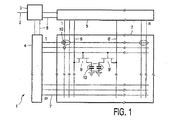
図1は、本発明が適用できる表示装置1の一部の電気等価回路を示す図である。その表示装置は、行又は選択電極7と2つの列又はデータ電極6、6´の交差領域における画素10のマトリクスを有する。行電極は行ドライバ4により連続的に選択される一方、列電極1、1´乃至n、n´はデータレジスタ5によりデータを供給される。このために、入力データ2は、先ず、必要に応じて、処理器11において処理される。行ドライバ4とデータレジスタ5との間の相互同期化は駆動ライン8により行われる。
FIG. 1 is a diagram showing an electrical equivalent circuit of a part of a
行ドライバからの駆動信号は、ゲートが行電極7に選択的に接続され、ソース電極21が列電極6、6´それぞれに電気的に接続される薄膜トランジスタ(TFT)9、9´によりピクチャ電極を選択する。第1列ドライバ6における信号は、TFT9を経由して第1ピクチャ電極に転送される。画素10がアースに接続される場合は、1つ又はそれ以上の対向電極により第3ピクチャ電極に転送される。図1の実施例においては、そのようなTFT9、9´は、1つの画素10のみに対して図示されている。
The drive signal from the row driver is such that the gate electrode is selectively connected to the
図2Aは、例えば、第3電極7を備えているガラス又は合成材料から成る第1基板11と第1電極6を備えた透明な第2基板12とを有する画素を示している。画素は、電気泳動媒体、即ち、例えば、黒色で正の荷電粒子14と黒色で負の荷電粒子14´とを有する白色流体で満たされている。透明な第2基板は、更に、第2電極6´に印加される電圧により中間的光学状態を実現するように、第2電極6´を有する。この第3スイッチング電極6´に印加される電圧は2つの光学状態間のスイッチングを支配する。
FIG. 2A shows a pixel having a
例えば、図2Aにおいて、第1光学状態が生成される。更に、第3電極7はアースに接続され、第1電極6及び第2電極6´の一6は第1電圧+V1に接続され、第1電極6及び第2電極6´の他6は第2電圧V2に接続され、それにより、V1>V2>0であり、黒色で正の荷電粒子14は、最も低い電位の電極であって、この場合、第3スイッチング電極7の方に移動する。黒色で負の荷電粒子14´は、最も高い電位であって、この場合、第1電極の方に移動し、第1電極6の真下の領域に存在する。観測方向15から見ると、画素は、ここでは、実質的には、第1電極6の近傍の部分を除いて、流体13の色を呈しており、その画素の色は、この実施例においては略白色である。図2Bにおける実施例においては、極限の光学状態が実現している。図2Bにおいては、第3電極7はアースに接続される一方、第1電極6及び第2電極6´は電圧−Vに接続されている。黒色で正の荷電粒子14は最も低い電位の方であって、この場合、第1基板12に沿って平行である第1電極6と第2電極6´との間に規定された電位面の方に移動し、黒色で負の荷電流市14´は、最も高い電位の方であって、この場合、第3電極7により規定された電位面の方に移動する。観測方向15から見ると、画素は、ここでは、黒色粒子14の色を呈している。同様な光学状態は、第1電極6及び第2電極6´が電圧+Vに接続され、第3電極7がアースに接続される場合に生じる。黒色で負の荷電粒子14´は、最も高い電位の方であって、この場合、第1基板12に沿って平行は電位面の方に移動し、黒色で正の荷電流市14は、最も低い電位の方であって、この場合、第3電極7により規定された電位面の方に移動する。観測方向15から見ると、画素は又、黒色粒子の色を呈している。
For example, in FIG. 2A, a first optical state is generated. Furthermore, the
図2Cにおいては、中間的光学状態を生成するように、第1電極6は第1電圧+V1に接続され、第2電極6´は第3電圧+V3に接続され、ここでは、V1>V3>0及びV3<V2であるため、第3電極7はアースに接続される。黒色で正の荷電粒子14は、最も低い電位であって、この場合、第3電極7の周りの領域の方に移動する。黒色で負の荷電粒子14´は第1電極6の周りの領域の方に移動する。観測方向15から見ると、画素は、ここでは、部分的に黒色粒子の色で、部分的に白色流体の色を呈している。それ故、灰色の色合いが得られる。第2電極6´に印加される電圧V3の大きさを変化させることにより、種々のグレーシェーディングが得られる。図3は、電極6、6´及び7に印加される電圧の4つの有効な組み合わせに対する電位線と、正の荷電粒子に作用する力を示す矢印16とを示している。この場合、第1の灰色の色合いを有する第1画像がディスプレイ上に表示される。第2の灰色の色合いを有する続く第2画像は、第1電極6が負の第1電圧−V1に接続され、第2電極6´が負電圧−V3に接続されることにより表示され、ここでは、V1<V3<0であり、第3電極7はアースに接続されたままである。この場合、正の荷電粒子14は最も低い電位であって、この場合、第1電極6近傍の領域の方に移動する。負の荷電粒子14´は、第3電極7近傍の領域の方に移動し、それ故、新しい灰色の色合いが得られる。黒色粒子14の量が基板の下に存在し、それ故、灰色の色合いは、第1電極6及び第2電極6´における電圧V1及びV3の大きさに依存する。次に続く画像は、第1電極6を再び正電圧+V1に、第2電極6´を再び正電圧+V3も接続することにより表示される。各々の更に続く画像は、第3電極に関して、第1電極6及び第2電極6´それぞれに印加される電圧V1及びV3の極性を変化させることにより表示される。従来の電気泳動ディスプレイに比較して、本発明のディスプレイの優位性は、第1基板12から粒子14、14´全てを解放するリセットパルスを印加することなく、連続画像を表示することができることである。この方法においては、表示スクリーンの一時的ブランキングを回避できる。
In FIG. 2C, the
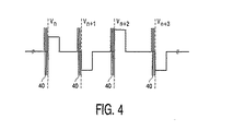
好適には、各々の新しい画像の前に、応答時間を改善するために、少数のプレパルスが、データパルスV1及びV3に先立って第1電極6及び第2電極6´に印加される。図4は、画素10の電極6、6´の一方又は両方に印加されるデータパルスVn、Vn+1、Vn+2、Vn+3と4つのプレパルス40の組み合わせを示している。第1電極6に印加されるプレパルス40の大きさ及び持続時間は、第1電極6近傍の第1領域における電気泳動粒子14、14´を解放するに十分であるが、第3電極7近傍の領域にそれらを移動させるには小さすぎるエネルギーと結び付いている。好適には、最後のプレパルス40の極性は、第1電極6及び第2電極6´に印加される電圧V1及びV3の極性と逆である。代替として、プレパルス40は、電圧V1及びV2が電極6及び6´に印加される前に、第3電極7に印加されることができる。
Preferably, before each new image, a small number of pre-pulses are applied to the
基板11、12は、疎水性層であって、例えば、基板に荷電粒子14、14´の付着を回避するためにテトラフルオロエチレンを備えることが可能である。
The
代替として、文献、“Micro−encapsulated ELectrophoretic Materials for Electronic Paper Displays,20th IDRC conference,pp.84−87(2000)”に記載されているようなマイクロカプセルにカプセル化されることができる。電気泳動媒体、即ち、正の荷電粒子14及び負の荷電粒子14´を有する流体が、ここでは、透明基板又は結合剤におけるマイクロカプセルにおいて存在する。
Alternatively, it can be encapsulated in a microcapsule as described in the literature, “Micro-encapsulated Electromaterials for Electronic Paper Displays, 20th IDRC conference, pp. 84-87 (2000)”. An electrophoretic medium, ie a fluid having positively charged
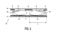
図5は、2つのマイクロカプセル16を有する表示装置の一部の断面50を示しており、第3電極7は又、アースに接続される一方、第1電極6及び第2電極6´は電圧V1及びV2それぞれに接続されている。マイクロカプセル16の横方向の大きさLは、第1電極6と第2電極6´との間の距離に略等しい。
FIG. 5 shows a
同時提出の特許請求の範囲における範囲から逸脱することなく、本発明の範囲内で多くの変形が可能であることは明白であろう。 It will be apparent that many variations are possible within the scope of the present invention without departing from the scope of the appended claims.
Claims (9)
電気泳動粒子の2つの群であって、正に帯電した電気泳動粒子の1つの群と負に帯電にした電気泳動粒子の1つの群とを有し、第1群の電気泳動粒子の色は第2群の電気泳動粒子の色と同じである、電気泳動粒子の2つの群;
駆動信号を受信するための各々の表示素子に関連付けられた第1電極、第2電極及び第3電極;並びに
表示される情報に従って、中間的光学状態を実現するために前記電極に前記駆動信号を印加するための制御手段;
を有することを特徴とする電気泳動表示装置。 An electrophoretic display device for displaying information comprising:
There are two groups of electrophoretic particles, one group of positively charged electrophoretic particles and one group of negatively charged electrophoretic particles, and the color of the electrophoretic particles of the first group is Two groups of electrophoretic particles that are the same color as the electrophoretic particles of the second group;
A first electrode, a second electrode and a third electrode associated with each display element for receiving a drive signal; and according to the information displayed, the drive signal is applied to the electrode to achieve an intermediate optical state Control means for applying;
An electrophoretic display device comprising:
The electrophoretic display device according to claim 1, wherein the electrophoretic medium is present in a microcapsule.
Applications Claiming Priority (2)
| Application Number | Priority Date | Filing Date | Title |
|---|---|---|---|
| EP02079333 | 2002-10-18 | ||
| PCT/IB2003/003928 WO2004036305A1 (en) | 2002-10-18 | 2003-09-12 | Electrophoretic display device |
Publications (1)
| Publication Number | Publication Date |
|---|---|
| JP2006503320A true JP2006503320A (en) | 2006-01-26 |
Family
ID=32103957
Family Applications (1)
| Application Number | Title | Priority Date | Filing Date |
|---|---|---|---|
| JP2004544523A Withdrawn JP2006503320A (en) | 2002-10-18 | 2003-09-12 | Electroluminescence display device |
Country Status (10)
| Country | Link |
|---|---|
| US (1) | US7145547B2 (en) |
| EP (1) | EP1556734B1 (en) |
| JP (1) | JP2006503320A (en) |
| KR (1) | KR20050049547A (en) |
| CN (1) | CN1688925A (en) |
| AT (1) | ATE320022T1 (en) |
| AU (1) | AU2003256024A1 (en) |
| DE (1) | DE60303965T2 (en) |
| TW (1) | TW200410035A (en) |
| WO (1) | WO2004036305A1 (en) |
Cited By (2)
| Publication number | Priority date | Publication date | Assignee | Title |
|---|---|---|---|---|
| JP2010528340A (en) * | 2007-05-21 | 2010-08-19 | イー インク コーポレイション | Method for driving a video electro-optic display |
| JP2022553989A (en) * | 2019-11-14 | 2022-12-27 | イー インク コーポレイション | Electro-optic medium containing oppositely charged particles and variable transmission device incorporating same |
Families Citing this family (20)
| Publication number | Priority date | Publication date | Assignee | Title |
|---|---|---|---|---|
| US20110199671A1 (en) * | 2002-06-13 | 2011-08-18 | E Ink Corporation | Methods for driving electrophoretic displays using dielectrophoretic forces |
| JP4522101B2 (en) * | 2004-01-27 | 2010-08-11 | キヤノン株式会社 | Electrophoretic display device and driving method of electrophoretic display device |
| JP4378771B2 (en) * | 2004-12-28 | 2009-12-09 | セイコーエプソン株式会社 | Electrophoresis device, electrophoretic device driving method, and electronic apparatus |
| EP1938302B1 (en) * | 2005-10-14 | 2014-11-12 | Koninklijke Philips N.V. | In-plane switching display devices |
| US7821701B2 (en) * | 2006-06-30 | 2010-10-26 | Koninklijke Philips Electronics N.V. | Electrophoretic display with homogeneously distributed electrically charged particles |
| EP1950729B1 (en) * | 2007-01-29 | 2012-12-26 | Seiko Epson Corporation | Drive method for display device, drive device, display device, and electronic device |
| EP2269114A1 (en) * | 2008-02-26 | 2011-01-05 | Hewlett-Packard Development Company, L.P. | Passive electrophoretic liquid crystal display device |
| US8570636B2 (en) * | 2008-04-18 | 2013-10-29 | Zikon Inc. | Systems, methods and compositions relating to display elements |
| KR101544589B1 (en) | 2009-01-14 | 2015-08-13 | 삼성전자주식회사 | Display apparatus using dielectrophoresis and method of manufacturing the display apparatus |
| TWI396032B (en) * | 2009-10-28 | 2013-05-11 | Au Optronics Corp | Electro-phoretic display pixel structure and display apparatus |
| JP5593738B2 (en) * | 2010-03-03 | 2014-09-24 | セイコーエプソン株式会社 | Driving method of electrophoretic display device |
| JP5387452B2 (en) * | 2010-03-04 | 2014-01-15 | セイコーエプソン株式会社 | Driving method of electrophoretic display device |
| JP5499785B2 (en) * | 2010-03-08 | 2014-05-21 | セイコーエプソン株式会社 | Driving method of electrophoretic display device |
| JP2011237770A (en) | 2010-04-12 | 2011-11-24 | Seiko Epson Corp | Electrophoresis display device, driving method of the same and electronic equipment |
| JP2011237771A (en) * | 2010-04-12 | 2011-11-24 | Seiko Epson Corp | Electrophoresis display device and electronic equipment |
| CN102243846A (en) * | 2011-07-14 | 2011-11-16 | 福州大学 | Method and circuit for modulating grey level of electronic paper |
| JP5972604B2 (en) * | 2012-02-27 | 2016-08-17 | イー インク コーポレイション | Electrophoretic display dispersion, display medium, and display device |
| JP2013231824A (en) * | 2012-04-27 | 2013-11-14 | Mitsubishi Pencil Co Ltd | Electrophoretic display device and drive method of the same |
| CN115047686B (en) * | 2021-11-24 | 2023-05-09 | 荣耀终端有限公司 | Electronic ink screen and display device |
| CN115762428B (en) * | 2022-11-23 | 2023-08-15 | 广州文石信息科技有限公司 | Display device and system based on electronic ink screen |
Family Cites Families (8)
| Publication number | Priority date | Publication date | Assignee | Title |
|---|---|---|---|---|
| US6538801B2 (en) * | 1996-07-19 | 2003-03-25 | E Ink Corporation | Electrophoretic displays using nanoparticles |
| EP1070276B1 (en) * | 1998-04-10 | 2005-06-01 | E-Ink Corporation | Full color reflective display with multichromatic sub-pixels |
| US6462859B1 (en) * | 2000-10-04 | 2002-10-08 | 3M Innovative Properties Company | Electromagnetically responsive particle assembly and methods and articles for manufacture and use |
| TW574512B (en) * | 2001-03-14 | 2004-02-01 | Koninkl Philips Electronics Nv | Electrophoretic display device |
| JP4568477B2 (en) * | 2001-04-02 | 2010-10-27 | イー インク コーポレイション | Electrophoretic media with improved image stability |
| US6822783B2 (en) * | 2001-06-26 | 2004-11-23 | Canon Kabushiki Kaisha | Electrophoretic display unit, and driving method thereof |
| JP2003005226A (en) * | 2001-06-26 | 2003-01-08 | Canon Inc | Electrophoresis display device |
| US20050012707A1 (en) * | 2003-07-15 | 2005-01-20 | Hong-Da Liu | Electrophoretic display and a method of driving said display |
-
2003
- 2003-09-12 DE DE60303965T patent/DE60303965T2/en not_active Expired - Fee Related
- 2003-09-12 AU AU2003256024A patent/AU2003256024A1/en not_active Abandoned
- 2003-09-12 JP JP2004544523A patent/JP2006503320A/en not_active Withdrawn
- 2003-09-12 AT AT03808781T patent/ATE320022T1/en not_active IP Right Cessation
- 2003-09-12 US US10/531,613 patent/US7145547B2/en not_active Expired - Fee Related
- 2003-09-12 CN CNA038242842A patent/CN1688925A/en active Pending
- 2003-09-12 WO PCT/IB2003/003928 patent/WO2004036305A1/en active IP Right Grant
- 2003-09-12 KR KR1020057006450A patent/KR20050049547A/en not_active Application Discontinuation
- 2003-09-12 EP EP03808781A patent/EP1556734B1/en not_active Expired - Lifetime
- 2003-10-15 TW TW092128556A patent/TW200410035A/en unknown
Cited By (3)
| Publication number | Priority date | Publication date | Assignee | Title |
|---|---|---|---|---|
| JP2010528340A (en) * | 2007-05-21 | 2010-08-19 | イー インク コーポレイション | Method for driving a video electro-optic display |
| JP2022553989A (en) * | 2019-11-14 | 2022-12-27 | イー インク コーポレイション | Electro-optic medium containing oppositely charged particles and variable transmission device incorporating same |
| JP7480288B2 (en) | 2019-11-14 | 2024-05-09 | イー インク コーポレイション | Electro-optic medium containing oppositely charged particles and variable transmission device incorporating same - Patents.com |
Also Published As
| Publication number | Publication date |
|---|---|
| DE60303965D1 (en) | 2006-05-04 |
| EP1556734A1 (en) | 2005-07-27 |
| ATE320022T1 (en) | 2006-03-15 |
| KR20050049547A (en) | 2005-05-25 |
| TW200410035A (en) | 2004-06-16 |
| DE60303965T2 (en) | 2006-10-26 |
| AU2003256024A1 (en) | 2004-05-04 |
| US20050270267A1 (en) | 2005-12-08 |
| CN1688925A (en) | 2005-10-26 |
| US7145547B2 (en) | 2006-12-05 |
| WO2004036305A1 (en) | 2004-04-29 |
| EP1556734B1 (en) | 2006-03-08 |
Similar Documents
| Publication | Publication Date | Title |
|---|---|---|
| US20210312874A1 (en) | Driving methods with variable frame time | |
| JP2006503320A (en) | Electroluminescence display device | |
| US8558855B2 (en) | Driving methods for electrophoretic displays | |
| US9019318B2 (en) | Driving methods for electrophoretic displays employing grey level waveforms | |
| KR101232146B1 (en) | Electrophoretic Display Device | |
| US8576163B2 (en) | Electrophoretic display device, method of driving the same, and electronic apparatus | |
| CN101042512B (en) | Electrophoresis device, electronic apparatus, and method of driving electrophoresis device | |
| US20040119680A1 (en) | Switching of two-particle electrophoretic display media with a combination of AC and DC electric field for contrast enhancement | |
| CN110140165B (en) | Display device and driving method | |
| KR20070112943A (en) | Electronic ink panel and electronic ink-display device having the same and method driving for the same | |
| JP5317007B2 (en) | Electro-optical device, driving method of electro-optical device, and electronic apparatus | |
| TW201033715A (en) | Multiple voltage level driving for electrophoretic displays | |
| JP4860487B2 (en) | Electrophoretic display panel | |
| US6791740B2 (en) | Electro-optical device, method of driving electro-optical device, and electronic apparatus | |
| JP2007163987A (en) | Electrophoretic display | |
| JP5217410B2 (en) | Drive device and image display device | |
| JP5504632B2 (en) | Electrophoresis device, electrophoretic device driving method, and electronic apparatus | |
| JP5445310B2 (en) | Electrophoretic display device, control circuit, electronic apparatus, and driving method | |
| KR101163605B1 (en) | Display device of electronic ink type and method for driving the same | |
| KR20230003578A (en) | Electro-optical displays and methods for driving them | |
| US11580919B2 (en) | Driving method of display device | |
| JP4529350B2 (en) | Electro-optical device and electronic apparatus | |
| JP6371078B2 (en) | Image display device, image display control device, and image display program | |
| JP6522881B2 (en) | Display medium drive device, display medium drive program, and display device | |
| JP2010032635A (en) | Electrophoresis device, driving method of electrophoresis device, and electronic device |
Legal Events
| Date | Code | Title | Description |
|---|---|---|---|
| A621 | Written request for application examination |
Free format text: JAPANESE INTERMEDIATE CODE: A621 Effective date: 20060911 |
|
| A761 | Written withdrawal of application |
Free format text: JAPANESE INTERMEDIATE CODE: A761 Effective date: 20061208 |