JP2006502507A - Method and system for thread-based memory access in a multi-thread processor - Google Patents
Method and system for thread-based memory access in a multi-thread processor Download PDFInfo
- Publication number
- JP2006502507A JP2006502507A JP2004543571A JP2004543571A JP2006502507A JP 2006502507 A JP2006502507 A JP 2006502507A JP 2004543571 A JP2004543571 A JP 2004543571A JP 2004543571 A JP2004543571 A JP 2004543571A JP 2006502507 A JP2006502507 A JP 2006502507A
- Authority
- JP
- Japan
- Prior art keywords
- thread
- memory
- processor
- identifier
- bank
- Prior art date
- Legal status (The legal status is an assumption and is not a legal conclusion. Google has not performed a legal analysis and makes no representation as to the accuracy of the status listed.)
- Withdrawn
Links
- 230000015654 memory Effects 0.000 title claims abstract description 194
- 238000000034 method Methods 0.000 title claims abstract description 38
- 238000012545 processing Methods 0.000 claims description 11
- 230000004913 activation Effects 0.000 claims description 4
- 238000004519 manufacturing process Methods 0.000 claims 2
- 238000005516 engineering process Methods 0.000 description 10
- 230000006870 function Effects 0.000 description 5
- 238000013507 mapping Methods 0.000 description 5
- 238000013461 design Methods 0.000 description 3
- 238000010586 diagram Methods 0.000 description 3
- 230000009467 reduction Effects 0.000 description 3
- 241001522296 Erithacus rubecula Species 0.000 description 2
- 238000012546 transfer Methods 0.000 description 2
- 101150005267 Add1 gene Proteins 0.000 description 1
- 101150060298 add2 gene Proteins 0.000 description 1
- 238000003491 array Methods 0.000 description 1
- 239000003795 chemical substances by application Substances 0.000 description 1
- 150000001875 compounds Chemical class 0.000 description 1
- 238000013500 data storage Methods 0.000 description 1
- 230000000694 effects Effects 0.000 description 1
- 230000007334 memory performance Effects 0.000 description 1
- 230000008569 process Effects 0.000 description 1
Images


Classifications
-
- G—PHYSICS
- G06—COMPUTING; CALCULATING OR COUNTING
- G06F—ELECTRIC DIGITAL DATA PROCESSING
- G06F12/00—Accessing, addressing or allocating within memory systems or architectures
- G06F12/02—Addressing or allocation; Relocation
- G06F12/08—Addressing or allocation; Relocation in hierarchically structured memory systems, e.g. virtual memory systems
- G06F12/0802—Addressing of a memory level in which the access to the desired data or data block requires associative addressing means, e.g. caches
- G06F12/0806—Multiuser, multiprocessor or multiprocessing cache systems
- G06F12/0842—Multiuser, multiprocessor or multiprocessing cache systems for multiprocessing or multitasking
-
- G—PHYSICS
- G06—COMPUTING; CALCULATING OR COUNTING
- G06F—ELECTRIC DIGITAL DATA PROCESSING
- G06F12/00—Accessing, addressing or allocating within memory systems or architectures
- G06F12/02—Addressing or allocation; Relocation
- G06F12/06—Addressing a physical block of locations, e.g. base addressing, module addressing, memory dedication
-
- G—PHYSICS
- G06—COMPUTING; CALCULATING OR COUNTING
- G06F—ELECTRIC DIGITAL DATA PROCESSING
- G06F12/00—Accessing, addressing or allocating within memory systems or architectures
- G06F12/02—Addressing or allocation; Relocation
- G06F12/08—Addressing or allocation; Relocation in hierarchically structured memory systems, e.g. virtual memory systems
- G06F12/0802—Addressing of a memory level in which the access to the desired data or data block requires associative addressing means, e.g. caches
- G06F12/0844—Multiple simultaneous or quasi-simultaneous cache accessing
- G06F12/0846—Cache with multiple tag or data arrays being simultaneously accessible
-
- G—PHYSICS
- G06—COMPUTING; CALCULATING OR COUNTING
- G06F—ELECTRIC DIGITAL DATA PROCESSING
- G06F9/00—Arrangements for program control, e.g. control units
- G06F9/06—Arrangements for program control, e.g. control units using stored programs, i.e. using an internal store of processing equipment to receive or retain programs
- G06F9/30—Arrangements for executing machine instructions, e.g. instruction decode
- G06F9/34—Addressing or accessing the instruction operand or the result ; Formation of operand address; Addressing modes
- G06F9/342—Extension of operand address space
-
- G—PHYSICS
- G06—COMPUTING; CALCULATING OR COUNTING
- G06F—ELECTRIC DIGITAL DATA PROCESSING
- G06F9/00—Arrangements for program control, e.g. control units
- G06F9/06—Arrangements for program control, e.g. control units using stored programs, i.e. using an internal store of processing equipment to receive or retain programs
- G06F9/30—Arrangements for executing machine instructions, e.g. instruction decode
- G06F9/38—Concurrent instruction execution, e.g. pipeline or look ahead
- G06F9/3824—Operand accessing
-
- G—PHYSICS
- G06—COMPUTING; CALCULATING OR COUNTING
- G06F—ELECTRIC DIGITAL DATA PROCESSING
- G06F9/00—Arrangements for program control, e.g. control units
- G06F9/06—Arrangements for program control, e.g. control units using stored programs, i.e. using an internal store of processing equipment to receive or retain programs
- G06F9/30—Arrangements for executing machine instructions, e.g. instruction decode
- G06F9/38—Concurrent instruction execution, e.g. pipeline or look ahead
- G06F9/3836—Instruction issuing, e.g. dynamic instruction scheduling or out of order instruction execution
- G06F9/3851—Instruction issuing, e.g. dynamic instruction scheduling or out of order instruction execution from multiple instruction streams, e.g. multistreaming
-
- Y—GENERAL TAGGING OF NEW TECHNOLOGICAL DEVELOPMENTS; GENERAL TAGGING OF CROSS-SECTIONAL TECHNOLOGIES SPANNING OVER SEVERAL SECTIONS OF THE IPC; TECHNICAL SUBJECTS COVERED BY FORMER USPC CROSS-REFERENCE ART COLLECTIONS [XRACs] AND DIGESTS
- Y02—TECHNOLOGIES OR APPLICATIONS FOR MITIGATION OR ADAPTATION AGAINST CLIMATE CHANGE
- Y02D—CLIMATE CHANGE MITIGATION TECHNOLOGIES IN INFORMATION AND COMMUNICATION TECHNOLOGIES [ICT], I.E. INFORMATION AND COMMUNICATION TECHNOLOGIES AIMING AT THE REDUCTION OF THEIR OWN ENERGY USE
- Y02D10/00—Energy efficient computing, e.g. low power processors, power management or thermal management
Landscapes
- Engineering & Computer Science (AREA)
- Theoretical Computer Science (AREA)
- Physics & Mathematics (AREA)
- General Engineering & Computer Science (AREA)
- General Physics & Mathematics (AREA)
- Software Systems (AREA)
- Multimedia (AREA)
- Memory System Of A Hierarchy Structure (AREA)
- Power Sources (AREA)
Abstract
多重スレッド・プロセッサによるスレッドをベースにしたメモリ・アクセスの技術が開示される。多重スレッド・プロセッサは、特定のプロセッサ・スレッドに関連付けられたスレッド識別子を決定し、さらにスレッド識別子の少なくとも部分を使用して、対応するプロセッサ・スレッドでアクセスすべき関連したメモリの特定部分を選択する。例示の実施形態では、スレッド識別子の第1の部分は、メモリの中の複数の複数バンク・メモリ要素のうちの1つを選択するために使用され、スレッド識別子の第2の部分は、複数バンク・メモリ要素の選ばれた1つの中の複数のメモリ・バンクのうちの1つを選択するために使用される。第1の部分は、スレッド識別子の1つまたは複数の最上位のビットを含み、一方で、第2の部分は、スレッド識別子の1つまたは複数の最下位のビットを含む。有利なことには、本発明は、メモリのアクセス時間および電力消費を減少し、同時にプロセッサ・スレッドの機能停止を防止する。A technique for thread-based memory access by a multi-thread processor is disclosed. The multi-thread processor determines a thread identifier associated with a particular processor thread and further uses at least a portion of the thread identifier to select a particular portion of associated memory to be accessed by the corresponding processor thread. . In the illustrated embodiment, the first portion of the thread identifier is used to select one of the plurality of multi-bank memory elements in the memory, and the second portion of the thread identifier is the plurality of banks. Used to select one of a plurality of memory banks in a selected one of the memory elements. The first portion includes one or more most significant bits of the thread identifier, while the second portion includes one or more least significant bits of the thread identifier. Advantageously, the present invention reduces memory access time and power consumption while at the same time preventing processor thread outages.
Description
本発明は、一般にディジタル・データ・プロセッサの分野に関し、より詳細には、多重スレッド・プロセッサで使用するためのメモリ・アクセス技術に関する。 The present invention relates generally to the field of digital data processors, and more particularly to memory access techniques for use with multi-threaded processors.
本発明は、「Multithreaded Processor With Efficient Processing For Convergence Device Applications」という名称の米国特許出願代理人事件整理番号1007−6、「Method and Apparatus for Register File Port Reduction in a Multithreaded Processor」という名称の代理人事件整理番号1007−7、および「Method and Apparatus for Token Triggered Multithreading」という名称の代理人事件整理番号1007−8に記載されている発明に関係している。これらの出願の全ては、本出願と共に同時に出願され、参照して本明細書に組み込まれる。 The present invention is based on US Patent Attorney Case Number 1007-6, “Method and Appratus for Registor Registered Registor Registor Regitor of the United States of America”. It relates to the invention described in reference number 1007-7 and agent case reference number 1007-8 named "Method and Apparatus for Token-Triggered Multithreading". All of these applications are filed concurrently with this application and are incorporated herein by reference.
メモリはプロセッサ設計の重要な態様である。よく知られているように、プロセッサは、異なる記憶要素の階層構造を含むメモリ・システムと共に使用されることが多い。例えば、M.J.Flynn,「Computer Architecture: Piplined and Parallel Processor Design」、Jones and Bartlett Publishers,Boston,MA,1995に述べられているように、例えばそのようなメモリ・システムは、補助記憶装置、主メモリ、およびキャッシュ・メモリを含むことができる。この文献は、参照して本明細書に組み込む。
メモリ性能は、一般に、アクセス時間および帯域幅のようなパラメータによって特徴づけられる。アクセス時間は、メモリにデータの特定部分を求めるプロセッサ要求と要求されたデータのプロセッサへの戻りの間の時間を意味する。メモリ帯域幅は、1単位時間当たりにメモリが対処することができるメモリ・アクセス要求の数を意味する。
Memory is an important aspect of processor design. As is well known, processors are often used with memory systems that include a hierarchical structure of different storage elements. For example, M.M. J. et al. As described in Flynn, “Computer Architecture: Pipelined and Parallel Processor Design”, Jones and Bartlett Publishers, Boston, MA, 1995, such memory systems include auxiliary memory, Memory can be included. This document is incorporated herein by reference.
Memory performance is generally characterized by parameters such as access time and bandwidth. Access time refers to the time between a processor request for a particular portion of data in memory and the return of the requested data to the processor. Memory bandwidth refers to the number of memory access requests that a memory can handle per unit time.
上で言及した例示のメモリ・システム構成のキャッシュ・メモリまたは主メモリのような所定のメモリは、複数バンクの形で編成することができる。メモリの部分は、モジュールとも呼ばれることがある。例えば、いくつかのバンクは単一のメモリ・モジュールに結合されるかもしれないし、または、いくつかのモジュールはバンクの1つを形成するように結合されるかもしれない。一般に、メモリ・アクセス中の任意の時間に、メモリのバンクの部分集合だけが活動状態であることができる。最も簡単な可能な配列では、単一プロセッサは、単一メモリ・モジュールに対して要求する。そして、プロセッサは活動を止め、モジュールのサービスを待つ。モジュールが応答したとき、プロセッサの活動が再開する。 A given memory, such as the cache memory or main memory of the example memory system configuration referred to above, can be organized in multiple banks. The portion of memory may also be called a module. For example, some banks may be combined into a single memory module, or some modules may be combined to form one of the banks. In general, only a subset of the banks of memory can be active at any time during a memory access. In the simplest possible arrangement, a single processor requires for a single memory module. The processor then stops and waits for module service. When the module responds, processor activity resumes.
各メモリ・モジュールは、少なくとも2つの重要なパラメータ、すなわちモジュール・アクセス時間とモジュール・サイクル時間を有する。モジュール・アクセス時間は、正しいアドレスが与えられた出力メモリ・バッファ・レジスタにデータを取り出すのに必要な時間である。モジュール・サイクル時間は、同じモジュールに向けられる要求の間の最小時間である。 Each memory module has at least two important parameters: module access time and module cycle time. Module access time is the time required to fetch data into the output memory buffer register given the correct address. Module cycle time is the minimum time between requests directed to the same module.
歴史的に、プロセッサおよびメモリは別個にパッケージされた。しかし、現代の集積技術では、複数のモジュールおよびバンクをプロセッサと共に単一集積回路チップ内に組み込むことができる。 Historically, the processor and memory were packaged separately. However, in modern integrated technology, multiple modules and banks can be incorporated with a processor in a single integrated circuit chip.
従来のメモリ・アクセス技術の重大な問題は、そのような技術は一般に多重スレッド・プロセッサ、すなわち複数の別個の命令シーケンスまたは「スレッド」の同時実行をサポートするプロセッサ、で使用するために最適化されていないことである。例えば、多重スレッド・プロセッサに適用されるとき従来メモリ・アクセス技術は、非常に多数の読出しおよび書込みポートを必要とすることが多く、これによって電力消費が過度に大きくなる。その上、多重スレッド・プロセッサに適用されるときそのような技術は、特定のプロセッサ・スレッドの機能停止およびメモリ・アクセス時間の増加をもたらすことがある。
前述のことから明らかなように、多重スレッド・プロセッサに関連付けられたメモリで使用するための改善されたメモリ・アクセス技術が要求されている。 As is apparent from the foregoing, there is a need for an improved memory access technique for use with memory associated with multithreaded processors.
本発明は、多重スレッド・プロセッサのための改善されたメモリ・アクセス技術を提供する。より詳細には、例示の実施形態の本発明のメモリ・アクセス技術は、プロセッサ・スレッドのメモリ・アクセスに関連付けられた機能停止が起こらないようなやり方で、多重スレッド・プロセッサに関連付けられたメモリにおいてスレッドをベースにしたバンク・アクセスを可能にする。 The present invention provides an improved memory access technique for a multi-thread processor. More particularly, the memory access technique of the present invention in the illustrated embodiment is implemented in a memory associated with a multi-thread processor in such a manner that the outage associated with processor thread memory access does not occur. Enable thread-based bank access.
本発明に従って、多重スレッド・プロセッサは、特定のプロセッサ・スレッドに関連付けられたスレッド識別子を決定し、さらにスレッド識別子の少なくとも部分を使用して、対応するプロセッサ・スレッドでアクセスすべき関連したメモリの特定の部分を選択する。例えば、スレッド識別子の第1の部分は、メモリの中の複数の複数バンク・メモリ要素のうちの1つを選択するために使用することができ、スレッド識別子の第2の部分は、複数バンク・メモリ要素の選ばれた1つの中の複数のメモリ・バンクのうちの1つを選択するために使用することができる。第1の部分は、スレッド識別子の1つまたは複数の最上位のビットを備える、一方で、第2の部分は、スレッド識別子の1つまたは複数の最下位のビットを備える。 In accordance with the present invention, a multi-thread processor determines a thread identifier associated with a particular processor thread and further uses at least a portion of the thread identifier to identify the associated memory to be accessed by the corresponding processor thread. Select the part. For example, the first portion of the thread identifier can be used to select one of a plurality of multi-bank memory elements in the memory, and the second portion of the thread identifier can be Can be used to select one of a plurality of memory banks in a selected one of the memory elements. The first part comprises one or more most significant bits of the thread identifier, while the second part comprises one or more least significant bits of the thread identifier.
より詳細な例として、複数バンク・メモリ要素の各々は、偶数のメモリ・バンクおよび奇数のメモリ・バンクを含むことができ、スレッド識別子の第2の部分の最下位ビットが、対応するプロセッサ・スレッドによるアクセスのために偶数メモリ・バンクと奇数メモリ・バンクのうちの1つを選択するように使用される。 As a more detailed example, each of the multiple bank memory elements can include an even number of memory banks and an odd number of memory banks, with the least significant bit of the second portion of the thread identifier being the corresponding processor thread. Is used to select one of an even memory bank and an odd memory bank for access.
本発明の他の態様は、トークン起動スレッディングおよびパイプライン命令処理に関する。例えば、多重スレッド・プロセッサは、トークン起動スレッディングを実施するように構成することができる。この型のスレッディングは、現在プロセッサ・クロック・サイクルに関連して、次のクロック・サイクルのための命令を発行することを許可される特定のハードウェア・スレッド・ユニットまたはコンテキストを識別するために、トークンを使用する。 Other aspects of the invention relate to token activated threading and pipeline instruction processing. For example, a multi-thread processor can be configured to implement token-initiated threading. This type of threading is related to the current processor clock cycle to identify a specific hardware thread unit or context that is allowed to issue instructions for the next clock cycle. Use tokens.
有利なことには、本発明は、プロセッサ性能の損失なしに、多重スレッド・プロセッサのメモリ・アクセス時間および電力消費を相当に減少する。例えば、例示の実施形態では、ただ単一のメモリ・ポートだけを使用して、単一のプロセッサ・サイクルで、2つの読出しまたは書込みメモリ・アクセスを達成することができる。 Advantageously, the present invention significantly reduces memory access time and power consumption of multithreaded processors without loss of processor performance. For example, in the illustrated embodiment, only a single memory port can be used to achieve two read or write memory accesses in a single processor cycle.
本発明は、それに関連付けられた主メモリ、多重スレッド・キャッシュ・メモリ、および多重スレッド・データ・メモリを有する多重スレッド・プロセッサで実施されるように本明細書で説明する。しかし、留意すべきことであるが、本発明は、例示の実施形態の特定の多重スレッド・プロセッサおよびメモリ構成を使用することを必要とせず、もっと一般的に、必要なメモリ・ポートの数の減少、したがって減少された電力消費を実現することが望ましい多重スレッド・プロセッサ・メモリ・アクセスのどんな用途でも使用するのに適している。 The present invention is described herein as implemented on a multi-thread processor having a main memory, a multi-thread cache memory, and a multi-thread data memory associated therewith. However, it should be noted that the present invention does not require the use of the particular multi-thread processor and memory configuration of the illustrated embodiment, and more generally, the number of memory ports required. It is suitable for use in any application of multi-threaded processor memory access where it is desirable to achieve a reduced and therefore reduced power consumption.
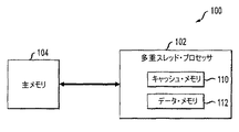
本発明に従ってメモリ・アクセス技術を実施する実施例の処理システム100を図1および2に関連して説明する。
An
図1は、主メモリ104に結合された多重スレッド・プロセッサ102を含むものとして、処理システム100を示す。多重スレッド・プロセッサ102は、多重スレッド・キャッシュ・メモリ110および多重スレッド・データ・メモリ112を含む。
FIG. 1 illustrates
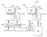
図2は、多重スレッド・プロセッサ102の1つの可能な実現のより詳細な図を示す。この実施形態では、多重スレッド・プロセッサ102は、多重スレッド・キャッシュ・メモリ110、データ・メモリ112、キャッシュ・コントローラ114、命令復号器116、レジスタ・ファイル118、および一組の演算論理ユニット(ALU)120を含む。多重スレッド・キャッシュ・メモリ110は、また、本明細書で多重スレッド・キャッシュとも呼ぶ。
FIG. 2 shows a more detailed view of one possible implementation of the
留意すべきことであるが、図1および2に示す特定の配列は、説明をはっきりさせるために簡単化されており、明示的に示されていない追加または代替えの要素を含めることができるが、このことは当業者には明らかであろう。 It should be noted that the particular arrangement shown in FIGS. 1 and 2 has been simplified for clarity of explanation and may include additional or alternative elements not explicitly shown, This will be apparent to those skilled in the art.
多重スレッド・キャッシュ110は、複数のスレッド・キャッシュ110−1、110−2、...、110−Nを含む。ここで、Nは、多重スレッド・プロセッサ102でサポートされるスレッドの番号を示す。したがって、各スレッドは、多重スレッド・キャッシュ110中にそのスレッドに関連付けられた対応するスレッド・キャッシュを有する。同様に、データ・メモリ112は、図示のように、データ・メモリ112−1、112−2、...、112−Nで示されるN個の別個のデータ・メモリ・インスタンスを有する。
The
多重スレッド・キャッシュ110のスレッド・キャッシュの各々は、1つまたは複数の組の記憶場所を有するメモリ・アレイを含むことができる。所定のスレッド・キャッシュは、さらに関連付けられたスレッド識別子を格納するためのスレッド識別子レジスタを備えることができるが、このことは、図6に関連して以下でより詳細に説明する。
Each of the thread caches of the
多重スレッド・キャッシュ110は、キャッシュ・コントローラ114を介して主メモリ104と接続して機能する。キャッシュ・コントローラ114は、主メモリ104からの適切な命令が多重スレッド・キャッシュ110にロードされることを保証する。この例示の実施形態のキャッシュ・コントローラ114は、個々のスレッド・キャッシュ110−1、110−2、...、110−Nと関連した論理回路または他の処理要素と共に動作し、完全アソシエティブ・マッピング、直接マッピングまたはセットアソシエティブ・マッピングのようなアドレス・マッピング技術の少なくとも一部を実施する。本発明と共に使用するのに適した例示のセットアソシエティブ・マッピング技術は、2002年6月4日に両方とも出願され本出願と共に一般的に譲渡された米国特許出願番号10/161,774および10/161,874に記載されている。これらの出願の両方を参照して本明細書に組み込む。
The
一般に、多重スレッド・キャッシュ110は、多重スレッド・プロセッサ102で実行されるべき命令を格納するために使用されるが、一方で、データ・メモリ112は、命令で処理されるデータを格納する。命令は、命令復号器116によって多重スレッド・キャッシュ110から取り出される。この命令復号器116は、従来のやり方で命令の実行を制御する際にレジスタ・ファイル118およびALU120と共に動作する。116、118および120のような多重スレッド・プロセッサ要素の動作は、当技術分野では十分に理解されているので、本明細書ではこれ以上詳細に説明しない。
In general, the
データ・メモリ112は、一般に、主メモリ104に直接に接続されているが、この接続は図に明示的に示されていない。
1つまたは複数のメモリ104、110および112は、各々、複数のバンクまたは他の指定された部分を含むように構成することができる。例として、各バンクは、1つまたは複数のメモリ・モジュールまたは単一メモリ・モジュールの指定された部分で構成されるものとみなすことができる。
One or
本明細書で使用されるような「メモリ」という用語は、内部または外部のメモリ、キャッシュ・メモリ、データ・メモリ、またはデータ記憶要素の他の配列を含むように広く解釈される意図である。本発明は、任意の特定のメモリの型、構成または用途に限定されない。しかし、留意すべきことであるが、メモリは一般に、図2のレジスタ・ファイル118を含むもののようなレジスタとまったく異なるものとして、プロセッサ技術分野で理解されている。レジスタ・ファイルへのスレッドをベースにしたアクセス技術は、「Method and Apparatus for Resistor File Port Reduction in a Multithreaded processor」という名称の上で引用した米国特許出願代理人事件整理番号1007−7に記載されている。 The term “memory” as used herein is intended to be broadly interpreted to include internal or external memory, cache memory, data memory, or other arrays of data storage elements. The present invention is not limited to any particular memory type, configuration or application. It should be noted, however, that memory is generally understood in the processor art as being quite different from registers such as those including the register file 118 of FIG. A thread-based access technology to the register file is described in US Patent Application Attorney Docket No. 1007-7, cited under the name “Method and Apparatus for Resistor File Port Reduction in a Multithreaded processor”. Yes.
また、強調すべきことであるが、本発明は、図2に示す特定の多重スレッド・プロセッサ構成を必要としない。本発明は、様々な他の多重スレッド・プロセッサ構成で実現することができる。 Also, it should be emphasized that the present invention does not require the specific multi-thread processor configuration shown in FIG. The present invention can be implemented in various other multi-thread processor configurations.
図2に示し、かつ本発明と共に使用するのに適した型の多重スレッド・プロセッサのより特別な例は、2001年12月20日に出願された米国仮出願番号60/341,289に記載されている。この出願は、参照して本明細書に組み込む。米国仮出願番号60/341,289に記載されているような多重スレッド・プロセッサの例示の実施形態は、RISCをベースにした制御コード、ディジタル信号プロセッサ(DSP)コード、Java(登録商標)コードおよびネットワーク処理コードを実行することができる。プロセッサは、単一命令複数データ(SIMD)・ベクトル・ユニット、リダクション・ユニット、および長命令語(LIW)複合命令実行を含む。 A more specific example of a multi-thread processor of the type shown in FIG. 2 and suitable for use with the present invention is described in US Provisional Application No. 60 / 341,289 filed on December 20, 2001. ing. This application is incorporated herein by reference. An exemplary embodiment of a multi-thread processor as described in US Provisional Application No. 60 / 341,289 includes RISC-based control code, digital signal processor (DSP) code, Java code, and Network processing code can be executed. The processor includes a single instruction multiple data (SIMD) vector unit, a reduction unit, and a long instruction word (LIW) compound instruction execution.
本発明の一態様に従って、多重スレッド・プロセッサ102に関連付けられたメモリは、別個の部分に分けられ、その部分の特定の1つは、対応するスレッド識別子を使用する所定のプロセッサ・スレッドによるアクセスのために選ばれる。より詳細には、例示の実施形態で、多重スレッド・プロセッサ102に関連付けられたメモリ・アクセス時間および電力要求は、どんな性能不利も招くことなく、各スレッドでバンキング・メモリの分だけ減少する。その上、スレッドをベースにしたバンキング方式は、プロセッサ・スレッドのメモリ・アクセスに関連付けられた機能停止を防ぐことができる。
In accordance with one aspect of the present invention, the memory associated with the
このように構成されたメモリは、例として、1つまたは複数の主メモリ104、キャッシュ・メモリ110、データ・メモリ112、または多重スレッド・プロセッサ102の中に含まれた他のメモリか、そうでなければ多重スレッド・プロセッサ102に関連付けられた他のメモリを含むことができる。このメモリ・アクセス技術の実施例の実施は、図3、4、5および6に関連して以下で説明する。
The memory thus configured may be, for example, one or more
多重スレッド・プロセッサ102は、トークン起動スレッディング技術と呼ばれるスレッディング方式、または他の適切なスレッディング技術を利用するように構成することができる。
The
図3は、スレッドの数Nが8であるプロセッサ102を実現するためのトークン起動スレッディングの実施例を示す。一般に、スレッドの全ては同時に動作し、各々がスレッド・キャッシュ110およびデータ・メモリ112の対応するインスタンスにアクセスする。図3に示すように、8個のスレッドは、スレッド0、スレッド1、スレッド2、...スレッド7で示され、リングの形に直列に相互接続されているものとして図示されている。多重スレッド・プロセッサでは、所定のスレッドは、一般に、ソフトウェアの点からだけでなくハードウェアの点からも見ることができる。したがって、所定のスレッドに関連付けられた特定のプロセッサ・ハードウェアは、本明細書で、特に、ハードウェア・スレッド・ユニットまたは単に「コンテキスト」と呼ぶ。
FIG. 3 shows an embodiment of token activation threading for realizing the
図3に示すトークン起動スレッディングに従って、ハードウェア・スレッド・ユニットまたはコンテキストの全ては、同時に命令を実行することができるが、ただ1つのコンテキストだけが、プロセッサの特定のクロック・サイクルで命令を発行することができる。言い換えると、全てのコンテキストは同時に実行するが、ただ1つのコンテキストだけが、特定のクロック・サイクルで活動状態である。したがって、合計でC個のコンテキストがある場合、全てのコンテキストから命令を発行するのにCクロック・サイクルが必要になる。クロック・サイクルごとに、コンテキストの1つが命令を発行し、命令を発行する次のスレッドがトークンで指示される。図3の実施例では、コンテキストが連続的に命令を発行するように、トークンは直列またはラウンド・ロビン状に配列されている。しかし、命令を発行する次のコンテキストを指示するトークンは、交互になる偶数・奇数パターンのような他のパターンを使用して配列することができる。または、上で言及したように、他の型のスレッディングを本発明と共に使用することができる。 According to the token-initiated threading shown in FIG. 3, all of the hardware thread units or contexts can execute instructions simultaneously, but only one context issues instructions in a particular clock cycle of the processor. be able to. In other words, all contexts execute at the same time, but only one context is active in a particular clock cycle. Thus, if there are a total of C contexts, C clock cycles are required to issue instructions from all contexts. Every clock cycle, one of the contexts issues an instruction, and the next thread issuing the instruction is pointed to by a token. In the embodiment of FIG. 3, the tokens are arranged in series or round robin so that the context issues instructions sequentially. However, tokens that indicate the next context to issue instructions can be arranged using other patterns, such as alternating even and odd patterns. Alternatively, as noted above, other types of threading can be used with the present invention.
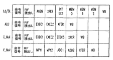
図4は、本発明に従った多重スレッド・プロセッサ102で、例の命令機能をパイプライン処理することができる方法を示す。本発明の例示の実施形態で、このパイプライン処理の型は、好ましくは、前に説明したトークン起動スレッディングと共に使用される。しかし、理解すべきことであるが、パイプライン処理およびスレッディングの他の数多くの組合せを、本発明を実施する際に使用することができる。
FIG. 4 illustrates how a
図4のパイプラインは、例示のN=8の図3のトークン起動スレッディングと共に使用するように構成されている。図4の例の命令機能は、ロード/格納(Ld/St)、ALU、整数乗算(I_Mul)、およびベクトル乗算(V_Mul)を含み、それぞれ9、6、7および8個のパイプライン段を有するものとして示されている。 The pipeline of FIG. 4 is configured for use with the exemplary N = 8 token activation threading of FIG. The example instruction functions of FIG. 4 include load / store (Ld / St), ALU, integer multiplication (I_Mul), and vector multiplication (V_Mul), with 9, 6, 7 and 8 pipeline stages, respectively. Shown as a thing.
図4に示した例の命令パイプラインの各々は、少なくとも、命令復号段、レジスタ・ファイル(RF)読出し段、転送(Xfer)段、およびライトバック(writeback)(WB)段を含む。RF読出し段は、レジスタ・ファイル、例えばレジスタ・ファイル118から読出すことを含み、転送段は、一般に、命令の結果を指定された保持レジスタに転送することを含み、そして、WB段は、命令の結果をメモリまたはレジスタ・ファイルに書き戻すことを含む。 Each of the example instruction pipelines shown in FIG. 4 includes at least an instruction decode stage, a register file (RF) read stage, a transfer (Xfer) stage, and a writeback (WB) stage. The RF read stage includes reading from a register file, eg, register file 118, the transfer stage generally includes transferring the result of the instruction to a designated holding register, and the WB stage includes the instruction To write back the result of this to a memory or register file.
Ld/Stパイプラインは、さらに、アドレス生成(Agen)段、内部(Int)または外部(Ext)決定段、および、Mem0、Mem1およびMem2と示される3個の追加メモリ実行段を含む。このように、Ld/Stパイプラインは、合計4個のメモリ実行段、すなわちMem0、Mem1、Mem2およびWBを含む。内部または外部決定段は、関連したメモリ・アクセスが内部メモリに対してであるかまたは外部メモリに対してであるかを決定し、それでパイプライン内の追加復号段とみなすことができる。留意すべきことであるが、追加のメモリ実行段は、ある特定の外部メモリ・アクセスのために必要とされるかもしれない。例えば、対応するスレッドが活動状態である期間の間に外部メモリ・アクセスのWB段が完成しない場合には、そのスレッドが活動状態である次の時間にWB段が完成するように、そのスレッドは機能を停止されるかもしれない。 The Ld / St pipeline further includes an address generation (Agen) stage, an internal (Int) or external (Ext) decision stage, and three additional memory execution stages denoted Mem0, Mem1 and Mem2. Thus, the Ld / St pipeline includes a total of four memory execution stages, namely Mem0, Mem1, Mem2, and WB. The internal or external decision stage determines whether the associated memory access is to internal memory or to external memory and can thus be considered as an additional decoding stage in the pipeline. It should be noted that additional memory execution stages may be required for certain external memory accesses. For example, if a WB stage of external memory access is not completed during the period in which the corresponding thread is active, the thread will be completed so that the WB stage is completed the next time the thread is active. May stop functioning.
ALUパイプラインは、さらに、Exec1およびExec2で示される2つの実行段を含む。 The ALU pipeline further includes two execution stages denoted Exec1 and Exec2.
整数I_Mulパイプラインは、さらに、Exec1、Exec2、およびExec3で示す3つの実行段を含む。 The integer I_Mul pipeline further includes three execution stages denoted as Exec1, Exec2, and Exec3.
ベクトルV_Mulパイプラインは、さらに、2つの乗算段MPY1およびMPY2、および2つの加算段Add1およびAdd2を含む。 The vector V_Mul pipeline further includes two multiplication stages MPY1 and MPY2 and two addition stages Add1 and Add2.
多重スレッド・プロセッサ102は、好ましくは、特定のコンテキストからの命令が対応するパイプラインに入るや否や、最後まで実行するように構成される。
図5は、多重スレッド・プロセッサ102の複数のコンテキストが連続するサイクルで命令を発行する簡単化されたパイプライン命令の例の組を示す。この実施例では、説明を簡単明瞭にするために、発行された命令各々は、命令取出し(IF)、読出し(RD)、実行(EX)およびライトバック(WB)で示される同じ4つのパイプライン段を含むものと想定する。さらに、図3に関連して説明されたものと同様な直列方法で、命令を発行する3つのスレッド、したがって3つのコンテキストがあるものと想定する。第1のクロック・サイクルで、コンテキストの第1のものによって、整数加算命令addir0、r2、8が最初に発行される。他の2つのコンテキストは、それぞれの後のクロック・サイクルで命令を発行する。各コンテキストが命令を発行するのに、合計で3クロック・サイクルかかる。第4のクロック・サイクルで、第1のコンテキストが別の命令、すなわち整数乗算命令mulir8、r0、4を発行する。
FIG. 5 illustrates an example set of simplified pipeline instructions in which multiple contexts of the
図5の実施例は、サイクルごとに1コンテキスト当たりただ単一の命令だけが発行されても、適切に構成されたパイプラインおよび十分な数のスレッドで、全てのハードウェア・コンテキストが同時に実行される可能性があることを説明するのに役立つ。前に示したように、特定の数のスレッドおよびパイプ段は説明の目的だけに過ぎず、好ましい実施形態を反映するつもりではない。当業者は、本明細書で与えられる教示を考慮にいれると、特定の用途のために適切な数のスレッドおよびパイプライン段を容易に決定することができる。 The embodiment of FIG. 5 allows all hardware contexts to execute simultaneously in a properly configured pipeline and a sufficient number of threads, even if only a single instruction is issued per context per cycle. Help explain what is possible. As indicated previously, the specific number of threads and pipe stages is for illustrative purposes only and is not intended to reflect the preferred embodiment. One skilled in the art can readily determine the appropriate number of threads and pipeline stages for a particular application, given the teachings provided herein.
上で言及したように、本発明は、その一態様に従って、多重スレッド・プロセッサ102で使用するための改善されたメモリ・アクセス技術を提供する。
As mentioned above, the present invention, according to one aspect thereof, provides an improved memory access technique for use with
一般に、この改善されたメモリ・アクセス技術は、多重スレッド・プロセッサの特定のスレッドに関連付けられたスレッド識別子を決定すること、および対応するプロセッサ・スレッドでアクセスすべきメモリの特定の部分を選ぶためにスレッド識別子の少なくとも部分を使用することを含む。 In general, this improved memory access technique is used to determine the thread identifier associated with a particular thread of a multi-thread processor and to select a particular portion of memory to be accessed by the corresponding processor thread. Using at least part of the thread identifier.
より詳細には、例示の配列では、多重スレッド・プロセッサでアクセスすべきメモリは、各々複数のメモリ・バンクを有するいくつかの別個のメモリ要素に分けて構成され、スレッド識別子の第1の部分はメモリの中の別個のメモリ要素のうちの1つを選択するために使用することができ、スレッド識別子の第2の部分はメモリ要素の選択された1つの中のメモリ・バンクのうちの1つを選択するために使用することができる。 More specifically, in the exemplary arrangement, the memory to be accessed by the multi-thread processor is organized into several separate memory elements, each having a plurality of memory banks, and the first part of the thread identifier is The second portion of the thread identifier can be used to select one of the separate memory elements in the memory, and the second part of the thread identifier is one of the memory banks in the selected one of the memory elements. Can be used to select.
複数バンク・メモリ要素の1つを選択するために使用されるスレッド識別子の第1の部分は、スレッド識別子の1つまたは複数の最上位のビットを含むことができるが、一方で、選択された複数バンク・メモリ要素の中のバンクの1つを選択するように使用されるスレッド識別子の第2の部分は、スレッド識別子の1つまたは複数の最下位のビットを含むことができる。 The first portion of the thread identifier used to select one of the multi-bank memory elements can include one or more most significant bits of the thread identifier, while selected The second portion of the thread identifier used to select one of the banks in the multi-bank memory element can include one or more least significant bits of the thread identifier.
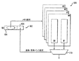
図6は、多重スレッド・プロセッサ102を使用する図1の処理システムで実施することができる、上述のメモリ・アクセス技術の1つの可能な実施形態を示す。この実施例では、多重スレッド・プロセッサ102の処理スレッドの数Nは8であると想定されている。図6は、M0、M1、M2およびM3で示す4つの複数バンク・メモリ要素を含むメモリ600を示す。メモリ600は、主メモリ104、キャッシュ・メモリ110、データ・メモリ112、または多重スレッド・プロセッサ102に関連付けられた他のメモリに対応するかもしれない。複数バンク・メモリ要素M0、M1、M2およびM3の各々は、本明細書でそれぞれ偶数メモリ・バンクおよび奇数メモリ・バンクとも呼ばれるB0およびB1で示された一対のメモリ・バンクを含む。
FIG. 6 illustrates one possible embodiment of the memory access technology described above that can be implemented in the processing system of FIG. 1 using a
スレッド識別子(TID)レジスタ602は、第1の部分604および第2の部分606を有するスレッド識別子を格納する。前に指摘したようにN=8であるこの実施例では、スレッド識別子は3ビットの識別子である。スレッド識別子の第1の部分604は、3ビット識別子の2つの最上位のビットを含み、4個の複数バンク・メモリ要素M0、M1、M2およびM3のうちの特定の1つを選択するために使用される。複数バンク・メモリ要素のうちの特定の1つを選択するために使用される選択回路は図6に明示的に示さないが、当業者は理解するであろうように、簡単なやり方で実施することができる。スレッド識別子の第2の部分606は、3ビット識別子の最下位ビットを含み、特定のメモリ・アクセスで使用するためのバンクのB0またはB1を選択する選択信号として、選択回路610に与えられる。
A thread identifier (TID) register 602 stores a thread identifier having a
図6のダイアグラムは読出しアクセスを示し、バンクB0とB1のうちの選択された1つから情報が読み出される。しかし、これはただ実施例としてだけであり、本発明は書込みアクセスにも使用することができる。 The diagram of FIG. 6 shows a read access, where information is read from a selected one of banks B0 and B1. However, this is only an example and the invention can also be used for write access.
図6の実施形態では、所定の複数バンク・メモリ要素M0、M1、M2またはM3は、読出しおよび書込みアクセスのために単一のメモリ・ポートを有しさえすればよい。例えば、本発明によって、偶数バンクと奇数バンクを交互にしてサイクルごとに複数バンク要素の各々から読み出すことができるようになる。その結果として、単一のメモリ・ポートは、あたかも実際には複数のメモリ・ポートを含むかのように機能することができる。より詳細には、1複数バンク・メモリ要素当たりにただ単一のメモリ・ポートだけを有する状態で、1プロセッサ・クロック・サイクル当たりに2つの読出しまたは書込みメモリ・アクセスを実現することができる。この配列は、メモリ・アクセス時間を減少し、また電力消費を低減するように使用することができるが、また同時にメモリ・アクセスによるプロセッサ・スレッド機能停止の問題が起こるのを防止する。 In the embodiment of FIG. 6, a given multi-bank memory element M0, M1, M2 or M3 need only have a single memory port for read and write access. For example, according to the present invention, even-numbered banks and odd-numbered banks can be alternately read from each of a plurality of bank elements every cycle. As a result, a single memory port can function as if it actually includes multiple memory ports. More specifically, two read or write memory accesses can be achieved per processor clock cycle with only a single memory port per multi-bank memory element. This arrangement can be used to reduce memory access time and reduce power consumption, but at the same time prevents the problem of processor thread stalling due to memory access.
本発明の技術を使用して、複数バンク・メモリ要素およびメモリ・バンクの数多くの他の構成が可能である。例えば、1つの可能な他の構成は、各々4個のメモリ・バンクを有する2個の複数バンク・メモリ要素を有することであり、この場合には、スレッド識別子の1つのビットは複数バンク・メモリ要素を選択するために使用され、スレッド識別子の2つのビットは、選択された複数バンク・メモリ要素の中の4個のメモリ・バンクのうちの1つを選択するために使用される。より詳細には、複数バンク・メモリ要素の数がMで与えられ、Bが1複数バンク・メモリ要素当たりのメモリ・バンクの数である場合、メモリは、MとBの積がNに等しいように、すなわちN=M*Bであるように構成することができる。他の配列もまた可能である。さらに、また留意すべきことであるが、各複数バンク・メモリ要素はメモリ・バンクと同数である必要は無い。 Many other configurations of multi-bank memory elements and memory banks are possible using the techniques of the present invention. For example, one possible other configuration is to have two multi-bank memory elements, each with four memory banks, in which case one bit of the thread identifier is multi-bank memory. Used to select an element, the two bits of the thread identifier are used to select one of the four memory banks in the selected multi-bank memory element. More specifically, if the number of multi-bank memory elements is given by M and B is the number of memory banks per multi-bank memory element, the memory is such that the product of M and B is equal to N. I.e., N = M * B. Other sequences are also possible. In addition, it should also be noted that each multi-bank memory element need not be the same number as the memory bank.
スレッド識別子レジスタ602および関連した選択回路は、多重スレッド・プロセッサ102の要素として実現することができる。例えば、メモリ600がキャッシュ・メモリ110に相当する本発明の実施形態では、この要素の全体または部分を、キャッシュ・コントローラ114の中に、または多重スレッド・プロセッサ102の他の部分の中に実現することができる。
The
スレッド識別子レジスタ602は、特定のスレッドを識別するために多重スレッド・プロセッサ102で使用される多ビット・スレッド識別子を格納する。そのようなスレッド識別子は従来のやり方で生成することができるが、このことは当業者には明らかであろう。
Thread identifier register 602 stores a multi-bit thread identifier that is used by
本明細書で使用されるような「スレッド識別子」という用語は、多重スレッド・プロセッサの特定のスレッドまたは一組の複数のスレッドを識別するのに適した任意の情報を含むつもりである。例としてまた制限することなく、スレッド識別子は多重スレッド・プロセッサのスレッド・カウンタの出力に対応するかもしれない。より詳細には、スレッド・カウンタ出力を実行される特定のスレッドを識別するために使用して、複数のスレッドがラウンド・ロビン順序のような予め決められた順序で処理されるようなぐあいに、所定の多重スレッド・プロセッサを構成することができる。そのような実施形態では、ラウンド・ロビン順序で処理される合計8個のスレッドがあり、その結果、処理される特定のスレッドを識別するために3ビット・カウンタの出力を使用するように、各スレッドが3ビット識別子で識別されるかもしれない。他の実施形態は、カウンタでないスレッド識別子の実施を使用することができる。本発明で使用するのに適した様々な異なるスレッド識別子構成は、当業者には容易に明らかであろう。 The term “thread identifier” as used herein is intended to include any information suitable for identifying a particular thread or set of multiple threads of a multi-thread processor. By way of example and without limitation, a thread identifier may correspond to the output of a multi-thread processor thread counter. More specifically, the thread counter output is used to identify a particular thread to be executed, while a plurality of threads are processed in a predetermined order, such as a round robin order. Multiple thread processors can be configured. In such an embodiment, there are a total of 8 threads that are processed in round-robin order, so that each uses a 3-bit counter output to identify the particular thread being processed. A thread may be identified with a 3-bit identifier. Other embodiments may use thread identifier implementations that are not counters. Various different thread identifier configurations suitable for use with the present invention will be readily apparent to those skilled in the art.
図6に示したようなメモリ・アクセス技術は、単一ビットのスレッド識別子を使用して、対応するプロセッサ・スレッドでアクセスすべき偶数または奇数のメモリ・バンクを選択する。しかし、スレッド識別子のn個の最下位のビットを使用して、所定の複数バンク・メモリ要素の2n個のメモリ・バンクのうちの1つを選択することが可能である。同様に、スレッド識別子のm個の最上位のビットを使用して、多重スレッド・プロセッサに関連付けられた所定のメモリの2m個の複数バンク・メモリ要素のうちの1つを選択することができる。 A memory access technique such as that shown in FIG. 6 uses a single bit thread identifier to select an even or odd memory bank to be accessed by the corresponding processor thread. However, it is possible to use the n least significant bits of the thread identifier to select one of the 2 n memory banks of a given multi-bank memory element. Similarly, the m most significant bits of the thread identifier can be used to select one of 2 m multi-bank memory elements of a given memory associated with the multi-thread processor. .
上で示したように、本発明のスレッドをベースにしたメモリ・アクセス技術は、従来技術に比べて大幅な改善を実現する。例えば、本技術は、メモリ・アクセス時間を改善することができる。また、本技術は、必要なメモリ・ポートの数を実質的に減らすことができ、それによって電力消費を低減する。さらに、これらの改善は、プロセッサ性能に影響を及ぼすことなく実現される。 As indicated above, the thread-based memory access technology of the present invention provides significant improvements over the prior art. For example, the present technology can improve memory access time. The technology can also substantially reduce the number of memory ports required, thereby reducing power consumption. Furthermore, these improvements are realized without affecting processor performance.
本発明の上述の実施形態は、ただ単に例示だけのつもりであり、添付の特許請求の範囲の範囲内の数多くの他の実施形態が当業者には明らかであろう。例えば、前に示したように、所定の複数バンク・メモリ要素は、図6のようなまさしく偶数バンクと奇数バンクを超えるものに分けることができる。すなわち、所定の複数バンク・メモリ要素内から所定のバンクを選択するために、スレッド識別子ビット数の適切な増加を使用して、複数バンク・メモリ要素をn個の別個の部分に分けることができる。他の実施例として、選択プロセスを実現するように使用される特定の選択回路配列を他の配列に取り替えることができる。さらに、多重スレッド・プロセッサ構成、スレッドの数、複数バンク・メモリ要素の数、1メモリ要素当たりのバンクの数、スレッド識別子構成、および例示の実施形態の他のパラメータは、所定の用途の特有の要求に対処するように変えることができる。 The above-described embodiments of the present invention are intended to be examples only, and many other embodiments within the scope of the appended claims will be apparent to those skilled in the art. For example, as previously indicated, a given multi-bank memory element can be divided into just over even and odd banks as in FIG. That is, an appropriate increase in the number of thread identifier bits can be used to divide a multi-bank memory element into n distinct parts to select a given bank from within a given multi-bank memory element. . As another example, the particular selection circuit arrangement used to implement the selection process can be replaced with another arrangement. Further, the multi-thread processor configuration, the number of threads, the number of multi-bank memory elements, the number of banks per memory element, the thread identifier configuration, and other parameters of the exemplary embodiment are specific to a given application. Can be changed to meet the requirements.
Claims (15)
前記多重スレッド・プロセッサの特定のスレッドに関連付けられたスレッド識別子を決定する工程と、
前記スレッド識別子の少なくとも部分を使用して、前記対応するプロセッサ・スレッドでアクセスすべき前記メモリの特定の部分を選択する工程と、を備える方法。 A method of accessing memory associated with a multi-thread processor, comprising:
Determining a thread identifier associated with a particular thread of the multi-thread processor;
Using at least a portion of the thread identifier to select a particular portion of the memory to be accessed by the corresponding processor thread.
前記多重スレッド・プロセッサに関連付けられたメモリと、を備えるプロセッサ・システムであって、
前記多重スレッド・プロセッサが、前記多重スレッド・プロセッサの特定のスレッドに関連付けられたスレッド識別子を決定し、かつ前記スレッド識別子の少なくとも部分を使用して前記対応するプロセッサ・スレッドでアクセスすべき前記メモリの特定の部分を選択するように動作するプロセッサ・システム。 A multi-thread processor;
A processor system comprising: a memory associated with the multi-thread processor;
The memory of the multi-thread processor to determine a thread identifier associated with a particular thread of the multi-thread processor and to be accessed by the corresponding processor thread using at least a portion of the thread identifier. A processor system that operates to select specific parts.
前記多重スレッド・プロセッサの特定のスレッドに関連付けられたスレッド識別子を決定する工程と、
前記スレッド識別子の少なくとも部分を使用して、前記対応するプロセッサ・スレッドでアクセスすべき前記メモリの特定の部分を選択する工程とを実施する製造物品。
An article of manufacture comprising a machine-readable storage medium having embodied program code for use in accessing memory associated with a multi-thread processor, wherein the program code when executed on the processor But,
Determining a thread identifier associated with a particular thread of the multi-thread processor;
An article of manufacture that implements using at least a portion of the thread identifier to select a particular portion of the memory to be accessed by the corresponding processor thread.
Applications Claiming Priority (2)
| Application Number | Priority Date | Filing Date | Title |
|---|---|---|---|
| US10/269,247 US6925643B2 (en) | 2002-10-11 | 2002-10-11 | Method and apparatus for thread-based memory access in a multithreaded processor |
| PCT/US2003/031961 WO2004034218A2 (en) | 2002-10-11 | 2003-10-09 | Method and apparatus for thread-based memory access in a multithreaded processor |
Publications (2)
| Publication Number | Publication Date |
|---|---|
| JP2006502507A true JP2006502507A (en) | 2006-01-19 |
| JP2006502507A5 JP2006502507A5 (en) | 2006-12-07 |
Family
ID=32068735
Family Applications (1)
| Application Number | Title | Priority Date | Filing Date |
|---|---|---|---|
| JP2004543571A Withdrawn JP2006502507A (en) | 2002-10-11 | 2003-10-09 | Method and system for thread-based memory access in a multi-thread processor |
Country Status (9)
| Country | Link |
|---|---|
| US (1) | US6925643B2 (en) |
| EP (1) | EP1550032B1 (en) |
| JP (1) | JP2006502507A (en) |
| KR (1) | KR100980536B1 (en) |
| CN (1) | CN1332303C (en) |
| AU (1) | AU2003282511A1 (en) |
| ES (1) | ES2758623T3 (en) |
| HU (1) | HUE046355T2 (en) |
| WO (1) | WO2004034218A2 (en) |
Cited By (1)
| Publication number | Priority date | Publication date | Assignee | Title |
|---|---|---|---|---|
| JP2016535913A (en) * | 2013-10-31 | 2016-11-17 | シリコン テーラー リミテッド | Pipelined configurable processor |
Families Citing this family (31)
| Publication number | Priority date | Publication date | Assignee | Title |
|---|---|---|---|---|
| KR100591755B1 (en) * | 2003-07-22 | 2006-06-22 | 삼성전자주식회사 | Apparatus and method for processing multiple threads simultaneously |
| US20050102494A1 (en) * | 2003-11-12 | 2005-05-12 | Grochowski Edward T. | Method and apparatus for register stack implementation using micro-operations |
| US7475222B2 (en) * | 2004-04-07 | 2009-01-06 | Sandbridge Technologies, Inc. | Multi-threaded processor having compound instruction and operation formats |
| US8074051B2 (en) | 2004-04-07 | 2011-12-06 | Aspen Acquisition Corporation | Multithreaded processor with multiple concurrent pipelines per thread |
| US7797363B2 (en) * | 2004-04-07 | 2010-09-14 | Sandbridge Technologies, Inc. | Processor having parallel vector multiply and reduce operations with sequential semantics |
| US7280428B2 (en) | 2004-09-30 | 2007-10-09 | Rambus Inc. | Multi-column addressing mode memory system including an integrated circuit memory device |
| US7797728B2 (en) * | 2004-10-27 | 2010-09-14 | Intel Corporation | Mechanism to generate restricted and unrestricted execution environments |
| TW200625097A (en) * | 2004-11-17 | 2006-07-16 | Sandbridge Technologies Inc | Data file storing multiple date types with controlled data access |
| US8595459B2 (en) | 2004-11-29 | 2013-11-26 | Rambus Inc. | Micro-threaded memory |
| US20060136681A1 (en) * | 2004-12-21 | 2006-06-22 | Sanjeev Jain | Method and apparatus to support multiple memory banks with a memory block |
| US20070223599A1 (en) * | 2005-07-25 | 2007-09-27 | Sysair, Inc., A Delaware Corporation | Cellular PC modem architecture and method of operation |
| WO2007033203A2 (en) | 2005-09-13 | 2007-03-22 | Freescale Semiconductor Inc. | Multi-threaded processor architecture |
| KR101305490B1 (en) * | 2005-10-01 | 2013-09-06 | 삼성전자주식회사 | The method and apparatus for mapping memory |
| US7584342B1 (en) * | 2005-12-15 | 2009-09-01 | Nvidia Corporation | Parallel data processing systems and methods using cooperative thread arrays and SIMD instruction issue |
| US7861060B1 (en) | 2005-12-15 | 2010-12-28 | Nvidia Corporation | Parallel data processing systems and methods using cooperative thread arrays and thread identifier values to determine processing behavior |
| US7788468B1 (en) | 2005-12-15 | 2010-08-31 | Nvidia Corporation | Synchronization of threads in a cooperative thread array |
| US20070260841A1 (en) * | 2006-05-02 | 2007-11-08 | Hampel Craig E | Memory module with reduced access granularity |
| JP5076418B2 (en) * | 2006-09-19 | 2012-11-21 | ソニー株式会社 | Shared memory device |
| US8819099B2 (en) * | 2006-09-26 | 2014-08-26 | Qualcomm Incorporated | Software implementation of matrix inversion in a wireless communication system |
| US9110726B2 (en) * | 2006-11-10 | 2015-08-18 | Qualcomm Incorporated | Method and system for parallelization of pipelined computations |
| US7596668B2 (en) * | 2007-02-20 | 2009-09-29 | International Business Machines Corporation | Method, system and program product for associating threads within non-related processes based on memory paging behaviors |
| EP2602710A1 (en) * | 2007-11-05 | 2013-06-12 | Aspen Acquisition Corporation | Method of encoding register instruction fields |
| WO2009097444A1 (en) * | 2008-01-30 | 2009-08-06 | Sandbridge Technologies, Inc. | Method for enabling multi-processor synchronization |
| KR20100133964A (en) * | 2008-03-13 | 2010-12-22 | 아스펜 액퀴지션 코포레이션 | Method for achieving power savings by disabling a valid array |
| JP2011530744A (en) | 2008-08-06 | 2011-12-22 | アスペン・アクイジション・コーポレーション | Stoppable and restartable DMA engine |
| CN101739242B (en) * | 2009-11-27 | 2013-07-31 | 深圳中微电科技有限公司 | Stream data processing method and stream processor |
| CN102141905B (en) * | 2010-01-29 | 2015-02-25 | 上海芯豪微电子有限公司 | Processor system structure |
| US9268719B2 (en) | 2011-08-05 | 2016-02-23 | Rambus Inc. | Memory signal buffers and modules supporting variable access granularity |
| US9436501B2 (en) | 2014-08-26 | 2016-09-06 | International Business Machines Corporation | Thread-based cache content saving for task switching |
| CN104461961B (en) * | 2014-11-20 | 2018-02-27 | 上海宝存信息科技有限公司 | The flash memory device and flash memory control method of a kind of Multi-core |
| CN112214243B (en) * | 2020-10-21 | 2022-05-27 | 上海壁仞智能科技有限公司 | Apparatus and method for configuring cooperative thread bundle in vector operation system |
Family Cites Families (19)
| Publication number | Priority date | Publication date | Assignee | Title |
|---|---|---|---|---|
| CA2094269A1 (en) * | 1990-10-19 | 1992-04-20 | Steven M. Oberlin | Scalable parallel vector computer system |
| US5682491A (en) | 1994-12-29 | 1997-10-28 | International Business Machines Corporation | Selective processing and routing of results among processors controlled by decoding instructions using mask value derived from instruction tag and processor identifier |
| US6128720A (en) | 1994-12-29 | 2000-10-03 | International Business Machines Corporation | Distributed processing array with component processors performing customized interpretation of instructions |
| US5649135A (en) | 1995-01-17 | 1997-07-15 | International Business Machines Corporation | Parallel processing system and method using surrogate instructions |
| US5659785A (en) | 1995-02-10 | 1997-08-19 | International Business Machines Corporation | Array processor communication architecture with broadcast processor instructions |
| GB2311882B (en) * | 1996-04-04 | 2000-08-09 | Videologic Ltd | A data processing management system |
| US6317872B1 (en) * | 1997-07-11 | 2001-11-13 | Rockwell Collins, Inc. | Real time processor optimized for executing JAVA programs |
| US6263404B1 (en) * | 1997-11-21 | 2001-07-17 | International Business Machines Corporation | Accessing data from a multiple entry fully associative cache buffer in a multithread data processing system |
| US6079010A (en) | 1998-03-31 | 2000-06-20 | Lucent Technologies Inc. | Multiple machine view execution in a computer system |
| US6317821B1 (en) | 1998-05-18 | 2001-11-13 | Lucent Technologies Inc. | Virtual single-cycle execution in pipelined processors |
| US6269425B1 (en) * | 1998-08-20 | 2001-07-31 | International Business Machines Corporation | Accessing data from a multiple entry fully associative cache buffer in a multithread data processing system |
| US6260189B1 (en) | 1998-09-14 | 2001-07-10 | Lucent Technologies Inc. | Compiler-controlled dynamic instruction dispatch in pipelined processors |
| US6256725B1 (en) | 1998-12-04 | 2001-07-03 | Agere Systems Guardian Corp. | Shared datapath processor utilizing stack-based and register-based storage spaces |
| US6341338B1 (en) * | 1999-02-04 | 2002-01-22 | Sun Microsystems, Inc. | Protocol for coordinating the distribution of shared memory |
| US6269437B1 (en) | 1999-03-22 | 2001-07-31 | Agere Systems Guardian Corp. | Duplicator interconnection methods and apparatus for reducing port pressure in a clustered processor |
| US6282585B1 (en) | 1999-03-22 | 2001-08-28 | Agere Systems Guardian Corp. | Cooperative interconnection for reducing port pressure in clustered microprocessors |
| US6230251B1 (en) | 1999-03-22 | 2001-05-08 | Agere Systems Guardian Corp. | File replication methods and apparatus for reducing port pressure in a clustered processor |
| US6351808B1 (en) * | 1999-05-11 | 2002-02-26 | Sun Microsystems, Inc. | Vertically and horizontally threaded processor with multidimensional storage for storing thread data |
| US20020103990A1 (en) | 2001-02-01 | 2002-08-01 | Hanan Potash | Programmed load precession machine |
-
2002
- 2002-10-11 US US10/269,247 patent/US6925643B2/en not_active Expired - Lifetime
-
2003
- 2003-10-09 HU HUE03774703A patent/HUE046355T2/en unknown
- 2003-10-09 EP EP03774703.7A patent/EP1550032B1/en not_active Expired - Lifetime
- 2003-10-09 CN CNB2003801023335A patent/CN1332303C/en not_active Expired - Lifetime
- 2003-10-09 AU AU2003282511A patent/AU2003282511A1/en not_active Abandoned
- 2003-10-09 WO PCT/US2003/031961 patent/WO2004034218A2/en active Application Filing
- 2003-10-09 KR KR1020057005888A patent/KR100980536B1/en active IP Right Grant
- 2003-10-09 ES ES03774703T patent/ES2758623T3/en not_active Expired - Lifetime
- 2003-10-09 JP JP2004543571A patent/JP2006502507A/en not_active Withdrawn
Cited By (2)
| Publication number | Priority date | Publication date | Assignee | Title |
|---|---|---|---|---|
| JP2016535913A (en) * | 2013-10-31 | 2016-11-17 | シリコン テーラー リミテッド | Pipelined configurable processor |
| US10275390B2 (en) | 2013-10-31 | 2019-04-30 | Silicon Tailor Limited | Pipelined configurable processor |
Also Published As
| Publication number | Publication date |
|---|---|
| US20040073772A1 (en) | 2004-04-15 |
| KR20050046819A (en) | 2005-05-18 |
| CN1708747A (en) | 2005-12-14 |
| US6925643B2 (en) | 2005-08-02 |
| WO2004034218A3 (en) | 2004-06-03 |
| EP1550032A4 (en) | 2008-03-12 |
| EP1550032B1 (en) | 2019-09-11 |
| AU2003282511A8 (en) | 2004-05-04 |
| WO2004034218A2 (en) | 2004-04-22 |
| KR100980536B1 (en) | 2010-09-06 |
| CN1332303C (en) | 2007-08-15 |
| EP1550032A2 (en) | 2005-07-06 |
| ES2758623T3 (en) | 2020-05-06 |
| AU2003282511A1 (en) | 2004-05-04 |
| HUE046355T2 (en) | 2020-03-30 |
Similar Documents
| Publication | Publication Date | Title |
|---|---|---|
| US6925643B2 (en) | Method and apparatus for thread-based memory access in a multithreaded processor | |
| US6842848B2 (en) | Method and apparatus for token triggered multithreading | |
| EP1550030B1 (en) | Method and apparatus for register file port reduction in a multithreaded processor | |
| KR101303119B1 (en) | Multithreaded processor with multiple concurrent pipelines per thread | |
| EP1442374B1 (en) | Multi-core multi-thread processor | |
| US7904702B2 (en) | Compound instructions in a multi-threaded processor | |
| US20070239970A1 (en) | Apparatus For Cooperative Sharing Of Operand Access Port Of A Banked Register File | |
| TWI764966B (en) | A data processing apparatus and method for controlling vector memory accesses | |
| US7805590B2 (en) | Coprocessor receiving target address to process a function and to send data transfer instructions to main processor for execution to preserve cache coherence | |
| US20070300042A1 (en) | Method and apparatus for interfacing a processor and coprocessor | |
| US7925862B2 (en) | Coprocessor forwarding load and store instructions with displacement to main processor for cache coherent execution when program counter value falls within predetermined ranges | |
| US20080141252A1 (en) | Cascaded Delayed Execution Pipeline |
Legal Events
| Date | Code | Title | Description |
|---|---|---|---|
| A521 | Written amendment |
Free format text: JAPANESE INTERMEDIATE CODE: A523 Effective date: 20061006 |
|
| A621 | Written request for application examination |
Free format text: JAPANESE INTERMEDIATE CODE: A621 Effective date: 20061006 |
|
| A761 | Written withdrawal of application |
Free format text: JAPANESE INTERMEDIATE CODE: A761 Effective date: 20081128 |