JP2006323739A - Memory module, memory system and information apparatus - Google Patents
Memory module, memory system and information apparatus Download PDFInfo
- Publication number
- JP2006323739A JP2006323739A JP2005147957A JP2005147957A JP2006323739A JP 2006323739 A JP2006323739 A JP 2006323739A JP 2005147957 A JP2005147957 A JP 2005147957A JP 2005147957 A JP2005147957 A JP 2005147957A JP 2006323739 A JP2006323739 A JP 2006323739A
- Authority
- JP
- Japan
- Prior art keywords
- memory
- cache
- data
- interface
- address
- Prior art date
- Legal status (The legal status is an assumption and is not a legal conclusion. Google has not performed a legal analysis and makes no representation as to the accuracy of the status listed.)
- Pending
Links
Images


Classifications
-
- G—PHYSICS
- G06—COMPUTING; CALCULATING OR COUNTING
- G06F—ELECTRIC DIGITAL DATA PROCESSING
- G06F12/00—Accessing, addressing or allocating within memory systems or architectures
- G06F12/02—Addressing or allocation; Relocation
- G06F12/0223—User address space allocation, e.g. contiguous or non contiguous base addressing
- G06F12/023—Free address space management
- G06F12/0238—Memory management in non-volatile memory, e.g. resistive RAM or ferroelectric memory
- G06F12/0246—Memory management in non-volatile memory, e.g. resistive RAM or ferroelectric memory in block erasable memory, e.g. flash memory
-
- G—PHYSICS
- G06—COMPUTING; CALCULATING OR COUNTING
- G06F—ELECTRIC DIGITAL DATA PROCESSING
- G06F12/00—Accessing, addressing or allocating within memory systems or architectures
-
- G—PHYSICS
- G06—COMPUTING; CALCULATING OR COUNTING
- G06F—ELECTRIC DIGITAL DATA PROCESSING
- G06F11/00—Error detection; Error correction; Monitoring
- G06F11/07—Responding to the occurrence of a fault, e.g. fault tolerance
- G06F11/08—Error detection or correction by redundancy in data representation, e.g. by using checking codes
- G06F11/10—Adding special bits or symbols to the coded information, e.g. parity check, casting out 9's or 11's
- G06F11/1008—Adding special bits or symbols to the coded information, e.g. parity check, casting out 9's or 11's in individual solid state devices
- G06F11/1068—Adding special bits or symbols to the coded information, e.g. parity check, casting out 9's or 11's in individual solid state devices in sector programmable memories, e.g. flash disk
-
- G—PHYSICS
- G06—COMPUTING; CALCULATING OR COUNTING
- G06F—ELECTRIC DIGITAL DATA PROCESSING
- G06F12/00—Accessing, addressing or allocating within memory systems or architectures
- G06F12/02—Addressing or allocation; Relocation
- G06F12/08—Addressing or allocation; Relocation in hierarchically structured memory systems, e.g. virtual memory systems
- G06F12/0802—Addressing of a memory level in which the access to the desired data or data block requires associative addressing means, e.g. caches
- G06F12/0888—Addressing of a memory level in which the access to the desired data or data block requires associative addressing means, e.g. caches using selective caching, e.g. bypass
-
- G—PHYSICS
- G06—COMPUTING; CALCULATING OR COUNTING
- G06F—ELECTRIC DIGITAL DATA PROCESSING
- G06F12/00—Accessing, addressing or allocating within memory systems or architectures
- G06F12/02—Addressing or allocation; Relocation
- G06F12/08—Addressing or allocation; Relocation in hierarchically structured memory systems, e.g. virtual memory systems
- G06F12/0802—Addressing of a memory level in which the access to the desired data or data block requires associative addressing means, e.g. caches
- G06F12/0893—Caches characterised by their organisation or structure
-
- G—PHYSICS
- G11—INFORMATION STORAGE
- G11C—STATIC STORES
- G11C5/00—Details of stores covered by group G11C11/00
- G11C5/02—Disposition of storage elements, e.g. in the form of a matrix array
-
- G—PHYSICS
- G11—INFORMATION STORAGE
- G11C—STATIC STORES
- G11C7/00—Arrangements for writing information into, or reading information out from, a digital store
- G11C7/10—Input/output [I/O] data interface arrangements, e.g. I/O data control circuits, I/O data buffers
- G11C7/1006—Data managing, e.g. manipulating data before writing or reading out, data bus switches or control circuits therefor
-
- G—PHYSICS
- G06—COMPUTING; CALCULATING OR COUNTING
- G06F—ELECTRIC DIGITAL DATA PROCESSING
- G06F12/00—Accessing, addressing or allocating within memory systems or architectures
- G06F12/02—Addressing or allocation; Relocation
- G06F12/08—Addressing or allocation; Relocation in hierarchically structured memory systems, e.g. virtual memory systems
- G06F12/0802—Addressing of a memory level in which the access to the desired data or data block requires associative addressing means, e.g. caches
- G06F12/0862—Addressing of a memory level in which the access to the desired data or data block requires associative addressing means, e.g. caches with prefetch
-
- G—PHYSICS
- G06—COMPUTING; CALCULATING OR COUNTING
- G06F—ELECTRIC DIGITAL DATA PROCESSING
- G06F2212/00—Indexing scheme relating to accessing, addressing or allocation within memory systems or architectures
- G06F2212/20—Employing a main memory using a specific memory technology
- G06F2212/202—Non-volatile memory
- G06F2212/2022—Flash memory
-
- G—PHYSICS
- G11—INFORMATION STORAGE
- G11C—STATIC STORES
- G11C2207/00—Indexing scheme relating to arrangements for writing information into, or reading information out from, a digital store
- G11C2207/22—Control and timing of internal memory operations
- G11C2207/2245—Memory devices with an internal cache buffer
-
- H—ELECTRICITY
- H01—ELECTRIC ELEMENTS
- H01L—SEMICONDUCTOR DEVICES NOT COVERED BY CLASS H10
- H01L2224/00—Indexing scheme for arrangements for connecting or disconnecting semiconductor or solid-state bodies and methods related thereto as covered by H01L24/00
- H01L2224/01—Means for bonding being attached to, or being formed on, the surface to be connected, e.g. chip-to-package, die-attach, "first-level" interconnects; Manufacturing methods related thereto
- H01L2224/10—Bump connectors; Manufacturing methods related thereto
- H01L2224/15—Structure, shape, material or disposition of the bump connectors after the connecting process
- H01L2224/16—Structure, shape, material or disposition of the bump connectors after the connecting process of an individual bump connector
- H01L2224/161—Disposition
- H01L2224/16151—Disposition the bump connector connecting between a semiconductor or solid-state body and an item not being a semiconductor or solid-state body, e.g. chip-to-substrate, chip-to-passive
- H01L2224/16221—Disposition the bump connector connecting between a semiconductor or solid-state body and an item not being a semiconductor or solid-state body, e.g. chip-to-substrate, chip-to-passive the body and the item being stacked
- H01L2224/16225—Disposition the bump connector connecting between a semiconductor or solid-state body and an item not being a semiconductor or solid-state body, e.g. chip-to-substrate, chip-to-passive the body and the item being stacked the item being non-metallic, e.g. insulating substrate with or without metallisation
-
- H—ELECTRICITY
- H01—ELECTRIC ELEMENTS
- H01L—SEMICONDUCTOR DEVICES NOT COVERED BY CLASS H10
- H01L2224/00—Indexing scheme for arrangements for connecting or disconnecting semiconductor or solid-state bodies and methods related thereto as covered by H01L24/00
- H01L2224/01—Means for bonding being attached to, or being formed on, the surface to be connected, e.g. chip-to-package, die-attach, "first-level" interconnects; Manufacturing methods related thereto
- H01L2224/26—Layer connectors, e.g. plate connectors, solder or adhesive layers; Manufacturing methods related thereto
- H01L2224/31—Structure, shape, material or disposition of the layer connectors after the connecting process
- H01L2224/32—Structure, shape, material or disposition of the layer connectors after the connecting process of an individual layer connector
- H01L2224/321—Disposition
- H01L2224/32135—Disposition the layer connector connecting between different semiconductor or solid-state bodies, i.e. chip-to-chip
- H01L2224/32145—Disposition the layer connector connecting between different semiconductor or solid-state bodies, i.e. chip-to-chip the bodies being stacked
-
- H—ELECTRICITY
- H01—ELECTRIC ELEMENTS
- H01L—SEMICONDUCTOR DEVICES NOT COVERED BY CLASS H10
- H01L2224/00—Indexing scheme for arrangements for connecting or disconnecting semiconductor or solid-state bodies and methods related thereto as covered by H01L24/00
- H01L2224/01—Means for bonding being attached to, or being formed on, the surface to be connected, e.g. chip-to-package, die-attach, "first-level" interconnects; Manufacturing methods related thereto
- H01L2224/42—Wire connectors; Manufacturing methods related thereto
- H01L2224/47—Structure, shape, material or disposition of the wire connectors after the connecting process
- H01L2224/48—Structure, shape, material or disposition of the wire connectors after the connecting process of an individual wire connector
- H01L2224/4805—Shape
- H01L2224/4809—Loop shape
- H01L2224/48091—Arched
-
- H—ELECTRICITY
- H01—ELECTRIC ELEMENTS
- H01L—SEMICONDUCTOR DEVICES NOT COVERED BY CLASS H10
- H01L2224/00—Indexing scheme for arrangements for connecting or disconnecting semiconductor or solid-state bodies and methods related thereto as covered by H01L24/00
- H01L2224/01—Means for bonding being attached to, or being formed on, the surface to be connected, e.g. chip-to-package, die-attach, "first-level" interconnects; Manufacturing methods related thereto
- H01L2224/42—Wire connectors; Manufacturing methods related thereto
- H01L2224/47—Structure, shape, material or disposition of the wire connectors after the connecting process
- H01L2224/48—Structure, shape, material or disposition of the wire connectors after the connecting process of an individual wire connector
- H01L2224/481—Disposition
- H01L2224/48135—Connecting between different semiconductor or solid-state bodies, i.e. chip-to-chip
- H01L2224/48137—Connecting between different semiconductor or solid-state bodies, i.e. chip-to-chip the bodies being arranged next to each other, e.g. on a common substrate
-
- H—ELECTRICITY
- H01—ELECTRIC ELEMENTS
- H01L—SEMICONDUCTOR DEVICES NOT COVERED BY CLASS H10
- H01L2224/00—Indexing scheme for arrangements for connecting or disconnecting semiconductor or solid-state bodies and methods related thereto as covered by H01L24/00
- H01L2224/01—Means for bonding being attached to, or being formed on, the surface to be connected, e.g. chip-to-package, die-attach, "first-level" interconnects; Manufacturing methods related thereto
- H01L2224/42—Wire connectors; Manufacturing methods related thereto
- H01L2224/47—Structure, shape, material or disposition of the wire connectors after the connecting process
- H01L2224/48—Structure, shape, material or disposition of the wire connectors after the connecting process of an individual wire connector
- H01L2224/481—Disposition
- H01L2224/48135—Connecting between different semiconductor or solid-state bodies, i.e. chip-to-chip
- H01L2224/48145—Connecting between different semiconductor or solid-state bodies, i.e. chip-to-chip the bodies being stacked
-
- H—ELECTRICITY
- H01—ELECTRIC ELEMENTS
- H01L—SEMICONDUCTOR DEVICES NOT COVERED BY CLASS H10
- H01L2224/00—Indexing scheme for arrangements for connecting or disconnecting semiconductor or solid-state bodies and methods related thereto as covered by H01L24/00
- H01L2224/01—Means for bonding being attached to, or being formed on, the surface to be connected, e.g. chip-to-package, die-attach, "first-level" interconnects; Manufacturing methods related thereto
- H01L2224/42—Wire connectors; Manufacturing methods related thereto
- H01L2224/47—Structure, shape, material or disposition of the wire connectors after the connecting process
- H01L2224/48—Structure, shape, material or disposition of the wire connectors after the connecting process of an individual wire connector
- H01L2224/481—Disposition
- H01L2224/48151—Connecting between a semiconductor or solid-state body and an item not being a semiconductor or solid-state body, e.g. chip-to-substrate, chip-to-passive
- H01L2224/48221—Connecting between a semiconductor or solid-state body and an item not being a semiconductor or solid-state body, e.g. chip-to-substrate, chip-to-passive the body and the item being stacked
- H01L2224/48225—Connecting between a semiconductor or solid-state body and an item not being a semiconductor or solid-state body, e.g. chip-to-substrate, chip-to-passive the body and the item being stacked the item being non-metallic, e.g. insulating substrate with or without metallisation
- H01L2224/48227—Connecting between a semiconductor or solid-state body and an item not being a semiconductor or solid-state body, e.g. chip-to-substrate, chip-to-passive the body and the item being stacked the item being non-metallic, e.g. insulating substrate with or without metallisation connecting the wire to a bond pad of the item
-
- H—ELECTRICITY
- H01—ELECTRIC ELEMENTS
- H01L—SEMICONDUCTOR DEVICES NOT COVERED BY CLASS H10
- H01L2224/00—Indexing scheme for arrangements for connecting or disconnecting semiconductor or solid-state bodies and methods related thereto as covered by H01L24/00
- H01L2224/01—Means for bonding being attached to, or being formed on, the surface to be connected, e.g. chip-to-package, die-attach, "first-level" interconnects; Manufacturing methods related thereto
- H01L2224/42—Wire connectors; Manufacturing methods related thereto
- H01L2224/47—Structure, shape, material or disposition of the wire connectors after the connecting process
- H01L2224/49—Structure, shape, material or disposition of the wire connectors after the connecting process of a plurality of wire connectors
- H01L2224/491—Disposition
- H01L2224/4912—Layout
- H01L2224/49175—Parallel arrangements
-
- H—ELECTRICITY
- H01—ELECTRIC ELEMENTS
- H01L—SEMICONDUCTOR DEVICES NOT COVERED BY CLASS H10
- H01L2224/00—Indexing scheme for arrangements for connecting or disconnecting semiconductor or solid-state bodies and methods related thereto as covered by H01L24/00
- H01L2224/73—Means for bonding being of different types provided for in two or more of groups H01L2224/10, H01L2224/18, H01L2224/26, H01L2224/34, H01L2224/42, H01L2224/50, H01L2224/63, H01L2224/71
- H01L2224/732—Location after the connecting process
- H01L2224/73251—Location after the connecting process on different surfaces
- H01L2224/73253—Bump and layer connectors
-
- H—ELECTRICITY
- H01—ELECTRIC ELEMENTS
- H01L—SEMICONDUCTOR DEVICES NOT COVERED BY CLASS H10
- H01L2224/00—Indexing scheme for arrangements for connecting or disconnecting semiconductor or solid-state bodies and methods related thereto as covered by H01L24/00
- H01L2224/73—Means for bonding being of different types provided for in two or more of groups H01L2224/10, H01L2224/18, H01L2224/26, H01L2224/34, H01L2224/42, H01L2224/50, H01L2224/63, H01L2224/71
- H01L2224/732—Location after the connecting process
- H01L2224/73251—Location after the connecting process on different surfaces
- H01L2224/73265—Layer and wire connectors
-
- H—ELECTRICITY
- H01—ELECTRIC ELEMENTS
- H01L—SEMICONDUCTOR DEVICES NOT COVERED BY CLASS H10
- H01L2924/00—Indexing scheme for arrangements or methods for connecting or disconnecting semiconductor or solid-state bodies as covered by H01L24/00
- H01L2924/15—Details of package parts other than the semiconductor or other solid state devices to be connected
- H01L2924/151—Die mounting substrate
- H01L2924/153—Connection portion
- H01L2924/1531—Connection portion the connection portion being formed only on the surface of the substrate opposite to the die mounting surface
- H01L2924/15311—Connection portion the connection portion being formed only on the surface of the substrate opposite to the die mounting surface being a ball array, e.g. BGA
-
- H—ELECTRICITY
- H01—ELECTRIC ELEMENTS
- H01L—SEMICONDUCTOR DEVICES NOT COVERED BY CLASS H10
- H01L2924/00—Indexing scheme for arrangements or methods for connecting or disconnecting semiconductor or solid-state bodies as covered by H01L24/00
- H01L2924/15—Details of package parts other than the semiconductor or other solid state devices to be connected
- H01L2924/181—Encapsulation
Abstract
Description
本発明は、不揮発性メモリを含むメモリシステムおよびメモリシステムの制御方法に関する。 The present invention relates to a memory system including a nonvolatile memory and a control method of the memory system.
従来、フラッシュメモリ(32M bit容量)とスタティックランダムアクセスメモリ(NOR(4M bit容量))とがスタックチップでFBGA(Fine pitch Ball Grid Array)型パッケージに一体封止された複合型半導体メモリがある。フラッシュメモリとNORとは、FBGA型パッケージの入出力電極に対してアドレス入力端子とデータ入出力端子が共通化されている。但し各々の制御端子はそれぞれ独立とされている(例えば、非特許文献1参照。)。 Conventionally, there is a composite semiconductor memory in which a flash memory (32 Mbit capacity) and a static random access memory (NOR (4 Mbit capacity)) are integrally sealed in a FBGA (Fine pitch Ball Grid Array) type package with a stack chip. The flash memory and NOR share an address input terminal and a data input / output terminal with respect to the input / output electrodes of the FBGA type package. However, each control terminal is independent (for example, refer nonpatent literature 1).
また、フラッシュメモリチップとDRAMチップとがリードフレーム型パッケージに一体封止された複合型半導体メモリもある。この複合型半導体メモリはフラッシュメモリとDRAMとはパッケージの入出力電極に対してアドレス入力端子、データ入出力端子、及び制御端子が共通化されて入出力される(例えば、特許文献1の図1及び図15、特許文献2参照。)。 There is also a composite semiconductor memory in which a flash memory chip and a DRAM chip are integrally sealed in a lead frame type package. In this composite semiconductor memory, the flash memory and the DRAM are input / output with the address input terminal, the data input / output terminal, and the control terminal in common with respect to the input / output electrodes of the package (for example, FIG. And FIG. 15 and Patent Document 2).
また、主記憶装置として扱われるフラッシュメモリとキャッシュメモリとコントローラとCPUから構成されるシステムもある(例えば、特許文献3の図1参照。)。 In addition, there is a system including a flash memory, a cache memory, a controller, and a CPU that are handled as a main storage device (see, for example, FIG. 1 of Patent Document 3).
また、フラッシュメモリとDRAMと転送制御回路からなる半導体メモリもある(例えば、特許文献4の図2、特許文献5参照。)。
本願発明者等は、本願に先立って携帯電話及びそれに使用されるプロセッサと、フラッシュメモリと、ランダムアクセスメモリから構成されたメモリシステムとその動作について検討を行った。 Prior to the present application, the inventors of the present application examined a memory system including a mobile phone and a processor used therefor, a flash memory, and a random access memory and its operation.
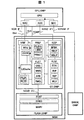
図33に示すように携帯電話には情報処理装置PRCとメモリモジュールMCMが使用されている。 As shown in FIG. 33, an information processing device PRC and a memory module MCM are used in a mobile phone.
情報処理装置PRCは中央演算装置CPUとSRAMコントローラから構成される。メモリモジュールMCMはNOR型フラッシュメモリNOR FLASHとSRAMから構成される。情報処理装置PRCはメモリモジュールMCMにアクセスを行い、データの読み出しおよび書き込みを行う。 The information processing apparatus PRC includes a central processing unit CPU and an SRAM controller. The memory module MCM includes a NOR flash memory NOR FLASH and SRAM. The information processing apparatus PRC accesses the memory module MCM, and reads and writes data.
電源投入後、情報処理装置PRCは、NOR型フラッシュメモリNOR FLASHに格納されているブートデータを読み出し、自らを立ち上げる。その後、情報処理装置PRCはNOR型フラッシュメモリNOR FLASHより必要に応じてアプリケーションプログラムを読みだし、中央演算装置CPUで実行する。SRAMはワークメモリとして機能し、中央演算装置CPUでの演算結果などが保存される。 After the power is turned on, the information processing apparatus PRC reads the boot data stored in the NOR flash memory NOR FLASH and starts up itself. Thereafter, the information processing apparatus PRC reads an application program from the NOR flash memory NOR FLASH as necessary, and executes it on the central processing unit CPU. The SRAM functions as a work memory, and stores the results of operations performed by the central processing unit CPU.
近年、携帯電話が取り扱うアプリケーション、データ、ワークエリアは携帯電話に付加される機能(音楽やゲーム等配信等)が増えるにつれて大きくなり、より大きな記憶容量のフラッシュメモリおよびランダムアクセスメモリが必要と予想される。さらに最近の携帯電話は高機能化が目覚しく、高速かつ大容量メモリのニーズが高まっている。 In recent years, applications, data, and work areas handled by mobile phones have become larger as functions added to mobile phones (distribution of music, games, etc.) increase, and it is expected that flash memory and random access memory with larger storage capacity will be required. The Furthermore, recent mobile phones are remarkably advanced in functionality, and the need for high-speed and large-capacity memory is increasing.
現在、携帯電話に用いられているNOR型フラッシュメモリは、NOR構成と呼ばれるメモリアレイ方式を用いたNOR型フラッシュメモリである。NOR型は、メモリセルアレイの寄生抵抗を小さく抑えたアレイ構成であり、並列接続したメモリセル2個につき1個の割合でメタルビット線コンタクトを設けることで低抵抗化を図っている。このため、読み出し時間は約80nsとNORの読み出し時間とほぼ同等にすることができる。しかし、その反面、セル2個につき1個のコンタクトを設ける必要があるため、コンタクト部のチップ面積に占める割合が高く、1ビットのメモリセル当たりの面積が大きくなり、大容量化には対応仕切れないという課題がある。 The NOR type flash memory currently used for mobile phones is a NOR type flash memory using a memory array system called a NOR configuration. The NOR type has an array configuration in which the parasitic resistance of the memory cell array is suppressed to a low level, and the resistance is reduced by providing one metal bit line contact for every two memory cells connected in parallel. For this reason, the read time can be approximately the same as the NOR read time of about 80 ns. However, since it is necessary to provide one contact for every two cells, the ratio of the contact area to the chip area is high, and the area per 1-bit memory cell is large. There is no problem.
また、代表的な大容量フラッシュメモリには、メモリアレイにAND構成を用いているAND型フラッシュメモリとNAND構成を用いているNAND型フラッシュメモリがある。これらのフラッシュメモリは、16〜128個のセルに対し1個のビット線コンタクトを設けるため、高密度のメモリアレイを実現できる。したがって、1ビットのメモリセル当たりの面積をNOR型フラッシュメモリより小さくでき、大容量化に対応できる。しかし、その反面、最初のデータを出力するまでの読み出し時間が、約25μsから100μsと遅く、NOR型フラッシュメモリとの整合性が取れないことが判明した。 Typical large-capacity flash memories include an AND flash memory using an AND configuration for a memory array and a NAND flash memory using a NAND configuration. Since these flash memories are provided with one bit line contact for 16 to 128 cells, a high-density memory array can be realized. Accordingly, the area per 1-bit memory cell can be made smaller than that of the NOR flash memory, and the capacity can be increased. However, on the other hand, it has been found that the read time until the first data is output is as slow as about 25 μs to 100 μs, and the consistency with the NOR type flash memory cannot be obtained.
フラッシュメモリは書き換えを繰り返すことによって、信頼性が低下し、書き込み時に書いたデータが、読み出し時には異なるデータとなったり、書き換え時にデータが書き込まれなかったりすることが稀にあることが判明した。 It has been found that by rewriting the flash memory, the reliability decreases, and the data written at the time of writing becomes different data at the time of reading or the data is rarely written at the time of rewriting.
また、半導体封止材中のウランなどの放射性物質から放出されるα線がランダムアクセスメモリRAMのメモリアレイに入射することによって、このメモリアレイに保持されている記憶データが破壊されることが稀にあり、ランダムアクセスメモリRAMの信頼性を劣化させる要因となっていることが判明した。 In addition, the α-rays emitted from radioactive substances such as uranium in the semiconductor encapsulant are incident on the memory array of the random access memory RAM, so that the stored data held in the memory array is rarely destroyed. It has been found that this is a factor that degrades the reliability of the random access memory RAM.
そこで本発明の目的の一つは、記憶容量が大きくかつ低コストで、使い勝手の良いROMとRAMを含むメモリシステムを提供することである。 Accordingly, one of the objects of the present invention is to provide a memory system including a ROM and a RAM that have a large storage capacity, are low in cost, and are easy to use.
本発明の代表的な手段を示せば以下の通りである。情報処理装置と、フラッシュメモリと、キャッシュメモリと、メモリコントローラを一つの封止体に実装し、封止体に半導体チップとの配線を行うための電極と、封止体と封止体外部との接続を行うための電極を設ける。 Representative means of the present invention are as follows. An information processing device, a flash memory, a cache memory, and a memory controller are mounted on one sealing body, an electrode for wiring the semiconductor chip to the sealing body, the sealing body and the sealing body outside, An electrode is provided for connection.
この際に、情報処理装置からのフラッシュメモリ内のデータの読み出し要求に対する読み出し時間を高速化するため、キャッシュメモリとフラッシュメモリへメモリコントローラを接続し、メモリコントローラによりフラッシュメモリからキャッシュメモリへデータ転送を行う。 At this time, in order to speed up the read time in response to the data read request from the information processing device, the memory controller is connected to the cache memory and the flash memory, and the memory controller transfers the data from the flash memory to the cache memory. Do.
電源投入後は、フラッシュメモリのデータの少なくとも一部をキャッシュメモリへ転送する制御を行うとよい。 After the power is turned on, control for transferring at least part of the data in the flash memory to the cache memory may be performed.
情報処理装置から入力したアドレスをキャッシュメモリのインデックスアドレスへ分散されるように制御すると良い。 Control may be performed so that addresses input from the information processing apparatus are distributed to the index addresses of the cache memory.
前記メモリコントローラは前もって、情報処置装置が利用するデータをキャッシュメモリへ転送するように制御すると良い。 The memory controller may be controlled in advance to transfer data used by the information processing apparatus to the cache memory.
また、フラッシュメモリ内のバッファをキャッシュメモリとして利用すると良い。 Further, it is preferable to use a buffer in the flash memory as a cache memory.
前記メモリコントローラはフラッシュメモリからデータを読み出し時は、エラー検出と訂正を行い、書きこみ時は、書きこみが正しく行われなかった不良アドレスに対して代替処理を行うと良い。また、フラッシュメモリ内のメモリセルへの書き込み回数を平均化する制御を行うと良い。さらに、キャッシュメモリからデータをも読み出した後エラー検出を行うと良い。 The memory controller may perform error detection and correction when reading data from the flash memory, and may perform substitution processing for defective addresses that were not correctly written during writing. Further, it is preferable to perform control for averaging the number of times of writing to the memory cells in the flash memory. Further, error detection may be performed after data is also read from the cache memory.
情報処理装置が要求したデータの到着を知ることができる信号線を設けると良い。 It is preferable to provide a signal line that can know the arrival of data requested by the information processing apparatus.
前記メモリコントローラは、キャッシュメモリからデータを読み出している間でも、前記情報処置装置よりフラッシュメモリへの読出し及び書きこみのアクセスを受付け、データの読出し及び書きこみが行われるように制御しても良い。 The memory controller may be configured to receive read and write access to the flash memory from the information processing apparatus and read and write data while reading data from the cache memory. .
高機能なメモリを実現できる。 A highly functional memory can be realized.
以下、本発明の実施の形態例につき添付図面を参照しながら詳細に説明する。実施の形態例において各ブロックを構成する回路素子は、特に制限されないが、公知のCMOS(相補型MOSトランジスタ)等の集積回路技術によって、単結晶シリコンのような1個の半導体基板上に形成される。 Embodiments of the present invention will be described in detail below with reference to the accompanying drawings. The circuit elements constituting each block in the embodiment are not particularly limited, but are formed on a single semiconductor substrate such as single crystal silicon by a known integrated circuit technology such as CMOS (complementary MOS transistor). The
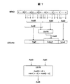
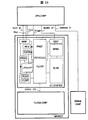
図1は本発明を適用した第1の実施の形態例である情報処理装置CPU_CHIPとメモリモジュールMSMとから構成されるメモリシステムを示したものである。以下におのおのについて説明する。 FIG. 1 shows a memory system composed of an information processing device CPU_CHIP and a memory module MSM, which is a first embodiment to which the present invention is applied. Each will be described below.
メモリモジュールMSMはFLASH_CHIPとCT_CHIPとから構成される。FLASH_CHIPは不揮発性メモリである。不揮発性メモリにはROM(リードオンリーメモリ)、EEPROM(エレクトリカリイレーサブルアンドプログラマブルROM)、フラッシュメモリ等を用いることができる。本実施の形態例ではフラッシュメモリを例に説明する。 The memory module MSM is composed of FLASH_CHIP and CT_CHIP. FLASH_CHIP is a nonvolatile memory. As the nonvolatile memory, ROM (read-only memory), EEPROM (electrically erasable and programmable ROM), flash memory, or the like can be used. In this embodiment, a flash memory will be described as an example.
代表的な大容量フラッシュメモリには、メモリアレイにAND構成を用いているAND型フラッシュメモリとNAND構成を用いているNAND型フラッシュメモリがあり、本発明には双方のフラッシュメモリを利用することができる。また、NANDインターフェースを装備している大容量フラッシュメモリと、ANDインターフェースを装備している大容量フラッシュメモリとがあり、本発明には双方のフラッシュメモリを利用することができる。本実施例ではNANDインターフェースを装備している大容量フラッシュメモリを例に説明する。 Typical large-capacity flash memories include an AND flash memory using an AND configuration and a NAND flash memory using a NAND configuration for the memory array. Both flash memories can be used in the present invention. it can. In addition, there are a large-capacity flash memory equipped with a NAND interface and a large-capacity flash memory equipped with an AND interface. Both flash memories can be used in the present invention. In this embodiment, a large-capacity flash memory equipped with a NAND interface will be described as an example.
特に限定しないが、FLASH_CHIPとして用いられる典型的なフラッシュメモリはNANDインターフェースを装備している大容量フラッシュメモリであり、約2Gbitの大きな記憶容量をもち、読み出し時間(読み出し要求からデータが出力されるまでの時間)は約25μsから100μsと比較的遅い。 Although not particularly limited, a typical flash memory used as FLASH_CHIP is a large-capacity flash memory equipped with a NAND interface, has a large storage capacity of about 2 Gbit, and has a read time (until data is output from a read request) Is relatively slow, about 25 μs to 100 μs.
DRAM_CHIPはダイナミックランダムアクセスメモリで内部構成やインターフェースの違いから、EDO(Extended Data Out)、SDRAM(Synchronous DRAM)、DDR(Double Data Rate)等様々な種類がある。メモリモジュールMSMにはいずれのDRAMでも用いることができる。本実施の形態例ではSDRAMを例に説明する。ダイナミックランダムアクセスメモリDRAM_CHIPは情報処理装置CPU_CHIPにてアプリケーションプログラムを実行するため一時的なワークメモリとして利用される。 DRAM_CHIP is a dynamic random access memory, and there are various types such as EDO (Extended Data Out), SDRAM (Synchronous DRAM), and DDR (Double Data Rate) due to differences in internal configuration and interface. Any DRAM can be used for the memory module MSM. In the present embodiment, an example of SDRAM will be described. The dynamic random access memory DRAM_CHIP is used as a temporary work memory for executing an application program in the information processing device CPU_CHIP.
特に限定しないが、DRAM_CHIPとして用いられる典型的なSDRAMは約256Mbitの大きな記憶容量を持っている。 Although not particularly limited, a typical SDRAM used as DRAM_CHIP has a large storage capacity of about 256 Mbit.
制御回路CT_CHIPは、FLASH_CHIPと情報処理装置CPU_CHIPとのデータ転送を制御する制御回路であり、特に限定しないが記憶容量が1MバイトであるキャッシュメモリL2Cacheを内蔵しており、読み出し時間は30nsから90ns程度で、従来のNOR型フラッシュより短時間あるいは同等である。 The control circuit CT_CHIP is a control circuit that controls data transfer between the FLASH_CHIP and the information processing device CPU_CHIP. Although not particularly limited, the control circuit CT_CHIP has a built-in cache memory L2Cache with a storage capacity of 1 Mbyte, and a read time of about 30 ns to 90 ns Therefore, it is shorter or equivalent to the conventional NOR type flash.
キャッシュメモリL2Cacheは、不揮発性メモリであるマグネティックランダムアクセスメモリMRAMおよび相変化メモリPRAMや、揮発性メモリであるスタティックランダムアクセスメモリSRAMにて実現でき、メモリモジュールMSMにはいずれのランダムアクセスメモリでも用いることができる。本実施の形態例では、キャッシュメモリL2Cacheに揮発性メモリであるスタティックランダムアクセスメモリSRAMを利用した例に説明する。 The cache memory L2Cache can be implemented with magnetic random access memory MRAM and phase change memory PRAM, which are non-volatile memories, and static random access memory SRAM, which is volatile memory, and any random access memory can be used for the memory module MSM. Can do. In the present embodiment, an example in which a static random access memory SRAM that is a volatile memory is used as the cache memory L2Cache will be described.
フラッシュメモリFLASH_CHIPと制御回路CT_CHIP間のデータ転送はNANDインターフェースNAND IF2で行われ、情報処理装置CPU_CHIPとイナミックランダムアクセスメモリDRAM_CHIPとのデータ転送はSDRAMインターフェースSDRAM IFで行われる。 Data transfer between the flash memory FLASH_CHIP and the control circuit CT_CHIP is performed by the NAND interface NAND IF2, and data transfer between the information processing device CPU_CHIP and the dynamic random access memory DRAM_CHIP is performed by the SDRAM interface SDRAM IF.
情報処理装置CPU_CHIPは中央演算装置CPUと、NORフラッシュコントローラNRCと、NANDフラッシュコントローラNDCと、DRAMコントローラSDCとから構成される。NORコントローラNRCはNORインターフェースでメモリモジュールMSM へアクセスを行い、データの読み書きを行う。DRAMコントローラSDCはSDRAMインターフェース(SDRAM IF)でDRAM_CHIPへアクセスを行いデータの読み書きを行う。 The information processing device CPU_CHIP includes a central processing unit CPU, a NOR flash controller NRC, a NAND flash controller NDC, and a DRAM controller SDC. The NOR controller NRC accesses the memory module MSM through the NOR interface, and reads and writes data. The DRAM controller SDC accesses the DRAM_CHIP through the SDRAM interface (SDRAM IF) to read / write data.
NANDフラッシュコントローラNDCは、NANDインターフェース(NAND IF1)でメモリモジュールMSM へアクセスを行い、データの読み書きを行う。 The NAND flash controller NDC accesses the memory module MSM through a NAND interface (NAND IF1), and reads and writes data.
フラッシュメモリFLASH_CHIPは、制御回路FCNTと、データバッファDREGと、メモリセルアレイMARYとから構成される。制御回路FCNTは、制御回路CT_CHIPのNANDインターフェースNAND IF2からの読み出し及び書き込み命令によって動作する回路である。 The flash memory FLASH_CHIP includes a control circuit FCNT, a data buffer DREG, and a memory cell array MARY. The control circuit FCNT is a circuit that operates according to read and write commands from the NAND interface NAND IF2 of the control circuit CT_CHIP.
読み出し要求が制御回路FCNTへ入力されると、メモリセルアレイMARYからデータバッファDREGへ、特に限定しないが、データサイズが2KB程度のデータが転送され、NANDインターフェースNAND IF2より制御回路CT_CHIPへ転送される。 When a read request is input to the control circuit FCNT, data having a data size of about 2 KB is transferred from the memory cell array MARY to the data buffer DREG, but is not limited thereto, and is transferred from the NAND interface NAND IF2 to the control circuit CT_CHIP.
また、データバッファDREGへ転送されたデータはそのまま保持される。 Further, the data transferred to the data buffer DREG is held as it is.
書き込み要求および書き込みデータが制御回路FCNTへ入力されると、特に限定しないが、データサイズが2KB程度のデータがデータバッファDREGへ入力され、最終的にメモリセルアレイMARYへ書き込まれる。また、データバッファDREGへ入力されたデータはそのまま保持される。 When a write request and write data are input to the control circuit FCNT, although not particularly limited, data having a data size of about 2 KB is input to the data buffer DREG and finally written to the memory cell array MARY. Further, the data input to the data buffer DREG is held as it is.
フラッシュメモリFLASH_CHIPは、特に制限はないが、メインデータ領域と代替領域REPAREAに分かれている。 The flash memory FLASH_CHIP is not particularly limited, but is divided into a main data area and an alternative area REPAREA.
メインデータ領域には初期プログラム領域が含まれており、初期プログラム領域内には、電源投入直後に、情報処理装置CPU_CHIPを立ち上げるためのブートプログラムと、フラッシュメモリFLASH_CHIPからキャッシュメモリL2Cacheへ自動転送するためのキャッシュ領域内のデータ範囲を示す自動転送領域指定データが格納されている。
<制御回路CT_CHIPの構成>
制御回路CT_CHIPは、NORインターフェース(NOR IF)からの読み出しおよび書き込み要求を受け取るNORインターフェース回路NRIF、NANDインターフェース(NAND IF)からの読み出しおよび書き込み要求を受け取るNANDインターフェース回路NDIF、レジスタブロックREG、アドレス変換回路DSTR、キャッシュメモリL2Cache、PL2A,PL2B、プリフェッチ制御回路PREF、フラッシュ制御回路FLCT、バッファ回路BFBK、フラッシュエラー制御回路FLSPから構成される。
The main data area includes an initial program area, and in the initial program area, immediately after power-on, a boot program for starting up the information processing device CPU_CHIP and automatic transfer from the flash memory FLASH_CHIP to the cache memory L2Cache The automatic transfer area designating data indicating the data range in the cache area is stored.
<Configuration of control circuit CT_CHIP>
The control circuit CT_CHIP includes a NOR interface circuit NRIF that receives read and write requests from the NOR interface (NOR IF), a NAND interface circuit NDIF that receives read and write requests from the NAND interface (NAND IF), a register block REG, and an address conversion circuit It comprises a DSTR, a cache memory L2Cache, PL2A, PL2B, a prefetch control circuit PREF, a flash control circuit FLCT, a buffer circuit BFBK, and a flash error control circuit FLSP.
キャッシュメモリL2Cacheは、特に限定しないが、1Mバイト程度の容量をもつ。また、キャッシュメモリPL2AおよびPL2Bは、特に限定しないが、それぞれ512バイトの容量を持つ。 The cache memory L2Cache is not particularly limited, but has a capacity of about 1 MB. Further, the cache memories PL2A and PL2B have a capacity of 512 bytes, although not particularly limited.
プリフェッチ制御回路PREFは、ヒット判定回路PL2Hit、L3Hit、先読み制御回路から構成される。バッファ回路BFBKは、リードバッファRBUF、書き込みバッファWBUFから構成される。 The prefetch control circuit PREF includes hit determination circuits PL2Hit and L3Hit and a prefetch control circuit. The buffer circuit BFBK includes a read buffer RBUF and a write buffer WBUF.
フラッシュ制御回路FLCTは、クロック制御回路OSC、メモリアドレス管理回路MMG、アクセス調停回路ARB、制御回路RWCLから構成される。 The flash control circuit FLCT includes a clock control circuit OSC, a memory address management circuit MMG, an access arbitration circuit ARB, and a control circuit RWCL.
フラッシュエラー制御回路FLSPは、エラー検出訂正回路ECC、バッファ回路BUF、代替処理回路REP、書き込み回数平均化回路WLVから構成される。 The flash error control circuit FLSP includes an error detection / correction circuit ECC, a buffer circuit BUF, an alternative processing circuit REP, and a write number averaging circuit WLV.
以下に本メモリシステムの動作を説明する。先ず、電源投入直後の動作について説明する。
<電源投入直後の動作説明>
情報処理装置CPU_CHIP、ダイナミックランダムアクセスメモリDRAM_CHIP、制御回路CT_CHIPおよびフラッシュメモリFLASH_CHIPへ電源投入を行うと、フラッシュ制御回路FLCTは、FLASH_CHIPの初期プログラム領域のデータをバッファ回路BUFへ読み出し、エラー検出訂正回路ECCにて、エラーがあるかどうかをチェックする。エラーがなければ、初期プログラム領域内のブートプログラムをキャッシュメモリPL2Aへ転送し、エラーがあれば訂正を行い、初期プログラム領域内のブートプログラムをキャッシュメモリPL2Aへ転送する。このように、電源投入直後にブートプログラムをFLASH_CHIPからキャッシュメモリPL2Aへ自動転送することにより、情報処理装置CPU_CHIPはこのブートプログラムを読み出し、すばやく自らを立ち上げ、さらにダイナミックランダムアクセスメモリDRAM_CHIPの初期設定を行うことができる。
The operation of this memory system will be described below. First, the operation immediately after the power is turned on will be described.
<Description of operation immediately after power-on>
When power is turned on to the information processing device CPU_CHIP, dynamic random access memory DRAM_CHIP, control circuit CT_CHIP, and flash memory FLASH_CHIP, the flash control circuit FLCT reads data in the initial program area of FLASH_CHIP to the buffer circuit BUF, and an error detection and correction circuit ECC Check if there is an error. If there is no error, the boot program in the initial program area is transferred to the cache memory PL2A. If there is an error, the boot program is corrected, and the boot program in the initial program area is transferred to the cache memory PL2A. In this way, by automatically transferring the boot program from FLASH_CHIP to the cache memory PL2A immediately after the power is turned on, the information processing device CPU_CHIP reads this boot program, quickly launches itself, and further initializes the dynamic random access memory DRAM_CHIP. It can be carried out.
情報処理装置CPU_CHIPが立ち上げを行っている間にフラッシュ制御回路FLCTは自動転送領域指定データをバッファ回路BUFより読み出し、このデータに示されている範囲のフラッシュメモリFLASH_CHIP内のデータをバッファ回路BUFへ順に読み出し、エラー検出訂正回路ECCにてエラーがあるかどうかをチェックする。エラーがなければ、キャッシュメモリPL2Bを経由しキャッシュメモリL2Cacheへ転送し、エラーがあれば訂正を行い、キャッシュメモリPL2Bを経由し、キャッシュメモリL2Cacheへ転送する。この自動データ転送が終了した時点で、メモリモジュールMSMは、一連の初期動作が終了したことを示す初期動作完了信号PCMPをHighにする。 While the information processing device CPU_CHIP is starting up, the flash control circuit FLCT reads the automatic transfer area designation data from the buffer circuit BUF, and the data in the flash memory FLASH_CHIP in the range indicated by this data is sent to the buffer circuit BUF. Read sequentially and check whether there is an error in the error detection and correction circuit ECC. If there is no error, it is transferred to the cache memory L2Cache via the cache memory PL2B, and if there is an error, it is corrected and transferred to the cache memory L2Cache via the cache memory PL2B. When this automatic data transfer is completed, the memory module MSM sets the initial operation completion signal PCMP indicating High to indicate that a series of initial operations has ended.
また、アクセス調停回路ARBは、レジスタブロックREGに対してデータ転送の完了を示す転送完了フラグを書き込む構成にしても良い。この場合、初期動作完了信号PCMPは必要ないため信号ピンを減らすことができる。 Further, the access arbitration circuit ARB may be configured to write a transfer completion flag indicating completion of data transfer to the register block REG. In this case, since the initial operation completion signal PCMP is not necessary, the number of signal pins can be reduced.
情報処理装置CPU_CHIPは、メモリモジュールMSMの初期動作完了信号PCMPをチェックすることによって電源投入直後のデータ転送が完了したことを知ることができるため、すぐにキャッシュメモリL2Cahceアクセスすることができる。 Since the information processing device CPU_CHIP can know that the data transfer immediately after power-on is completed by checking the initial operation completion signal PCMP of the memory module MSM, it can immediately access the cache memory L2Cahce.
このように、電源投入直後にブートプログラムをFLASH_CHIPからキャッシュメモリL2Cacheへ自動転送することにより、情報処理装置CPU_CHIPは、このブートデータを読み出し、すばやく自らを立ち上げることができる。さらに、情報処理装置CPU_CHIPが立ち上げを行っている間に、FLASH_CHIPのデータをキャッシュメモリL2Cacheへ自動転送することにより、情報処理装置CPU_CHIPが立ちあがった時点で、すぐにメモリモジュールMSMへアクセスすることができるため高性能化が図れる。
<レジスタブロックの説明>
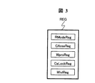
次に、レジスタブロックREGについて説明する。レジスタブロックREGには、特に限定しないが、読み出しモード設定レジスタRModeReg、キャッシュ領域設定レジスタCAreaReg、キャッシュロック領域設定レジスタCaLockReg、ライトプロテクト領域設定レジスタWproReg、書き込み回数平均化処理領域設定レジスタWlvlRegがある。
As described above, by automatically transferring the boot program from the FLASH_CHIP to the cache memory L2Cache immediately after the power is turned on, the information processing device CPU_CHIP can read this boot data and quickly start itself up. Furthermore, by automatically transferring the data of FLASH_CHIP to the cache memory L2Cache while the information processing device CPU_CHIP is starting up, the memory module MSM can be accessed immediately when the information processing device CPU_CHIP is started up. High performance can be achieved.
<Description of register block>
Next, the register block REG will be described. The register block REG includes, but is not limited to, a read mode setting register RModeReg, a cache area setting register CAreaReg, a cache lock area setting register CaLockReg, a write protect area setting register WproReg, and a write count averaging process area setting register WlvlReg.
キャッシュ領域および非キャッシュ領域を変更する場合は、特に限定しないが、NORインターフェースNOR IFからキャッシュ領域設定レジスタCAreaRegの値を書き換えることで、キャッシュ領域および非キャッシュ領域を変更することができる。特に限定しないが、電源投入直後には、フラッシュメモリFLASH_CHIPの全領域がキャッシュ領域となっている。 When changing the cache area and the non-cache area, the cache area and the non-cache area can be changed by rewriting the value of the cache area setting register CAreaReg from the NOR interface NOR IF. Although not particularly limited, immediately after the power is turned on, the entire area of the flash memory FLASH_CHIP is a cache area.
キャッシュ領域内データはキャッシュメモリL2Cache,PL2A,PL2Bへ転送され、非キャッシュ領域内データはキャッシュメモリL2Cache,PL2A,PL2Bへ転送されない。 Data in the cache area is transferred to the cache memories L2Cache, PL2A, and PL2B, and data in the non-cache area is not transferred to the cache memories L2Cache, PL2A, and PL2B.
キャッシュロック領域、非キャッシュロック領域を変更する場合は、特に限定しないが、NORインターフェースNOR IFからキャッシュ領域設定レジスタCAreaRegの値を書き換えることで、キャッシュロック領域、非キャッシュロック領域を変更することができる。特に限定しないが、電源投入直後には、フラッシュメモリFLASH_CHIPの全領域が非キャッシュロック領域となっている。 The cache lock area and the non-cache lock area are not particularly limited, but the cache lock area and the non-cache lock area can be changed by rewriting the value of the cache area setting register CAreaReg from the NOR interface NOR IF. . Although not particularly limited, immediately after the power is turned on, the entire area of the flash memory FLASH_CHIP is a non-cache lock area.
キャッシュロック領域内のデータは、一旦キャッシュメモリL2Cacheへ転送されると、キャッシュロック解除命令によってキャッシュ領域設定レジスタが書き換えられるまで、キャッシュメモリL2Cacheに存在することができる。また、非キャッシュロック領域内データは、キャッシュメモリL2Cacheから追い出される可能性がある。 Once the data in the cache lock area is transferred to the cache memory L2Cache, it can exist in the cache memory L2Cache until the cache area setting register is rewritten by a cache lock release instruction. Further, there is a possibility that data in the non-cache lock area is evicted from the cache memory L2Cache.
書き込み回数平均化処理領域、非書き込み回数平均化処理領域を変更する場合は、特に限定しないが、NORインターフェースNOR IFから書き込み回数平均化処理領域設定レジスタWlvlRegの値を書き換えることで、書き込み回数平均化処理領域、非書き込み回数平均化処理領域を変更することができる。特に限定しないが、電源投入直後には、フラッシュメモリFLASH_CHIPの半分の領域が書き込み回数平均化処理領域となっている。 When changing the write count averaging processing area and non-write count averaging process area, there is no particular limitation, but the number of writes is averaged by rewriting the value of the write count averaging process area setting register WLvlReg from the NOR interface NOR IF. The processing area and the non-write count averaging processing area can be changed. Although there is no particular limitation, immediately after the power is turned on, a half area of the flash memory FLASH_CHIP is a write frequency averaging process area.
書き込み回数平均化処理領域内データには、書き込み回数平均化回路WLVが、書き換えが集中していたと判断した場合は、書き込み回数平均化処理が行われる。 When the write number averaging circuit WLV determines that rewriting is concentrated on the data within the write number averaging process area, the write number average process is performed.
非書き込み回数平均化処理領域内データには書き込み回数平均化処理が行われない。 The write count averaging process is not performed on the data in the non-write count averaging process area.
ライトプロテクト領域、非ライトプロテクト領域を変更する場合は、特に限定しないが、NORインターフェースNOR IFからライトプロテクト領域設定レジスタWproRegの値を書き換えることで、ライトプロテクト領域、非ライトプロテクト領域を変更することができる。特に限定しないが、電源投入直後には、フラッシュメモリFLASH_CHIPの全領域が非ライトプロテクト領域となっている。 When changing the write protect area and non-write protect area, there is no particular limitation, but the write protect area and non-write protect area can be changed by rewriting the value of the write protect area setting register WproReg from the NOR interface NOR IF. it can. Although not particularly limited, immediately after the power is turned on, the entire area of the flash memory FLASH_CHIP is a non-write protected area.
ライトプロテクト領域には書き込みが行われず、非ライトプロテクト領域には、書込みが可能である。 Writing is not performed in the write protect area, and writing is possible in the non-write protect area.
メモリモジュールMSMが装備するNORインターフェースは、クロック信号CLKに同期して動作する同期型NORインターフェースと、クロック信号CLKには同期しない非同期型NORインターフェースであり、いずれかのNORインターフェースで動作する。特に限定しないが、メモリモジュールMSMは、電源投入直後には非同期NORインターフェースで動作する。 The NOR interface provided in the memory module MSM is a synchronous NOR interface that operates in synchronization with the clock signal CLK, and an asynchronous NOR interface that does not synchronize with the clock signal CLK, and operates with one of the NOR interfaces. Although not particularly limited, the memory module MSM operates with an asynchronous NOR interface immediately after power-on.
アドレス変換回路DSTRは、特に限定しないが、複数のアドレス変換方式(簡易インデックス変換方式、インデックスビットシフト変換方式、インデックス演算方式)を実現でき、いずれかのアドレス変換方式で動作する。特に限定しないが電源投入直後には、アドレス変換回路DSTRはインデックス演算方式にて動作する。 Although not particularly limited, the address conversion circuit DSTR can realize a plurality of address conversion methods (simple index conversion method, index bit shift conversion method, index calculation method), and operates in any one of the address conversion methods. Although there is no particular limitation, immediately after the power is turned on, the address conversion circuit DSTR operates by the index calculation method.
特に限定しないが、NORインターフェースNOR IFから読み出しモード設定レジスタRModeRegの値を書き換えることで、メモリモジュールMSMが装備するNORインターフェースやアドレス変換方式を変更することができる。 Although not particularly limited, the NOR interface and the address conversion method provided in the memory module MSM can be changed by rewriting the value of the read mode setting register RModeReg from the NOR interface NOR IF.
以上説明したように、同期型NORインターフェースや非同期型NORインターフェース、アドレス変換方式、キャッシュ領域および非キャッシュ領域、キャッシュロック領域および非キャッシュロック領域、書き込み回数平均化処理領域および非書き込み回数平均化処理領域、ライトプロテクト領域および非ライトプロテクト領域は、それぞれ独立に設定することができ、システムにあわせて利用者側で自由に選択できる。
<通常動作の説明>
電源投入時のパワーオンシーケンスが終了した後のフラッシュメモリFLASH_CHIPと情報処理装置CPU_CHIP間のデータ転送について説明する。
As described above, synchronous NOR interface and asynchronous NOR interface, address conversion method, cache area and non-cache area, cache lock area and non-cache lock area, write count averaging process area and non-write count averaging process area The write protect area and the non-write protect area can be set independently, and can be freely selected by the user according to the system.
<Description of normal operation>
Data transfer between the flash memory FLASH_CHIP and the information processing device CPU_CHIP after the power-on sequence at power-on is completed will be described.
先ず、情報処理装置CPU_CHIPがNORインターフェースNOR IFより読み出し要求を入力した場合の動作について説明する。 First, an operation when the information processing device CPU_CHIP inputs a read request from the NOR interface NOR IF will be described.
情報処理装置CPU_CHIPがNORインターフェース(NOR IF)より読み出し命令およびアドレスRADDを制御回路CT_CHIPへ入力すると、制御回路CT_CHIP 内のNORインターフェース回路NRIFは、これらの読み出し命令およびアドレスを保持する。NORインターフェース回路NRIFへ保持された読み出し命令及びアドレスRADDはメモリアドレス管理回路MMG、アクセス調停回路ARBおよびアドレス変換回路DSTRへ入力される。 When the information processing device CPU_CHIP inputs a read command and an address RADD from the NOR interface (NOR IF) to the control circuit CT_CHIP, the NOR interface circuit NRIF in the control circuit CT_CHIP holds these read commands and addresses. The read command and the address RADD held in the NOR interface circuit NRIF are input to the memory address management circuit MMG, the access arbitration circuit ARB, and the address conversion circuit DSTR.
メモリアドレス管理回路MMGはレジスタブロックREGに保持されているキャッシュ領域を示すアドレス情報とアドレスRADDとを比較する。 The memory address management circuit MMG compares the address information indicating the cache area held in the register block REG with the address RADD.
アドレスRADDがキャッシュ領域の範囲外であれば、キャッシュ領域範囲外情報がメモリアドレス管理回路MMGからNORインターフェース回路NRIFを通じてNORインターフェースNOR IFより情報処理装置CPU_CHIPへ通達される。 If the address RADD is out of the cache area, the out-of-cache area information is notified from the memory address management circuit MMG to the information processing device CPU_CHIP from the NOR interface NOR IF through the NOR interface circuit NRIF.
アクセス調停回路は、NORインターフェース回路NRIFから入力された読み出し要求と、NANDインターフェース回路NDIFからの読み出しや書き込み要求との調停を行う。 The access arbitration circuit arbitrates between a read request input from the NOR interface circuit NRIF and a read or write request from the NAND interface circuit NDIF.
まず、アクセス調停回路へNORインターフェース回路NRIFから読み出し要求が入力されると、アクセス調停回路は、NANDインターフェース回路NDIFからの読み出しや書き込み要求があるかないか、さらに、NANDインターフェース回路NDIFからの読み出しや書き込み要求に対する動作を行っているかどうかをチェックする。 First, when a read request is input from the NOR interface circuit NRIF to the access arbitration circuit, the access arbitration circuit checks whether there is a read or write request from the NAND interface circuit NDIF, and further reads or writes from the NAND interface circuit NDIF. Check if the request is being acted on.
NANDインターフェース回路NDIFからの読み出しや書き込み要求があり、この要求に対する動作がまだ行われていない場合は、NANDインターフェース回路NDIFからの読み出しや書き込み要求を後回しに、NORインターフェース回路NRIFから読み出し要求を優先的に許可する。 If there is a read or write request from the NAND interface circuit NDIF, and the operation for this request has not been performed yet, the read request from the NOR interface circuit NRIF is given priority to postpone the read or write request from the NAND interface circuit NDIF. To allow.
NANDインターフェース回路NDIFからの読み出しや書き込み要求に対する動作が実行中の場合は、この実行中の動作を一旦中断し、NORインターフェース回路NRIFから読み出し要求を優先的に許可する。 When an operation for a read or write request from the NAND interface circuit NDIF is being executed, the operation being executed is temporarily interrupted, and a read request is preferentially permitted from the NOR interface circuit NRIF.
アクセス調停回路へNANDインターフェース回路NDIFから読み出し及び書き込み要求が入力されると、アクセス調停回路は、NORインターフェース回路NRIFからの読み出しや書き込み要求があるかないか、さらに、NORインターフェース回路NRIFからの読み出しや書き込み要求に対する動作を行っているかどうかをチェックする。 When a read / write request is input from the NAND interface circuit NDIF to the access arbitration circuit, the access arbitration circuit checks whether there is a read / write request from the NOR interface circuit NRIF, and further reads / writes from the NOR interface circuit NRIF. Check if the request is being acted on.
NORインターフェース回路NRIFからの読み出しや書き込み要求に対する動作が実行中の場合は、この動作が完了して後に、NANDインターフェース回路NDIFから読み出し及び書き込み要求を許可する。 When an operation for a read or write request from the NOR interface circuit NRIF is being executed, the read / write request is permitted from the NAND interface circuit NDIF after the operation is completed.
NORインターフェース回路NRIFからの読み出しや書き込み要求がなく、この要求に対する動作が行われていない場合は、NANDインターフェース回路NDIFから読み出し及び書き込み要求を許可する。 When there is no read or write request from the NOR interface circuit NRIF and no operation is performed for this request, the read and write request is permitted from the NAND interface circuit NDIF.
アドレス変換回路は、キャッシュメモリL2Cache,PL2A,PL2Bの利用率やヒット率を高める目的で、アドレスRADDをアドレスMRADDへ変換する。 The address conversion circuit converts the address RADD into the address MRADD for the purpose of increasing the usage rate and hit rate of the cache memories L2Cache, PL2A, and PL2B.
アドレス変換回路によって変換されたアドレスMRADDは、キャッシュメモリL2Cache及びプリフェッチ制御回路PREFへ入力される。 The address MRADD converted by the address conversion circuit is input to the cache memory L2Cache and the prefetch control circuit PREF.
キャッシュメモリL2Cacheでは、先ず、アドレスMRADDで指定されたデータがキャッシュメモリL2Cache内に存在するかどうかのヒット判定を行う。アドレスMRADDで指定されたデータがキャッシュメモリL2Cache内に存在した場合はL2Cacheヒットとなり、存在しない場合はL2Cacheミスとなる。 In the cache memory L2Cache, first, a hit determination is made as to whether or not the data designated by the address MRADD exists in the cache memory L2Cache. If the data specified by the address MRADD exists in the cache memory L2Cache, an L2Cache hit occurs, and if it does not exist, an L2Cache miss occurs.
プリフェッチ制御回路PREF内のヒット判定回路PL2Hitでは、アドレスMRADDで指定されたデータがキャッシュメモリPLA2およびPL2Bのいずれかに存在するかどうかのヒット判定を行う。 The hit determination circuit PL2Hit in the prefetch control circuit PREF performs a hit determination as to whether or not the data specified by the address MRADD exists in either of the cache memories PLA2 and PL2B.
アドレスMRADDで指定されたデータがキャッシュメモリPL2A及びPL2Bのいずれかに存在した場合はPL2ヒットとなり、存在しない場合はPL2ミスとなる。 If the data specified by the address MRADD exists in either one of the cache memories PL2A and PL2B, a PL2 hit occurs. Otherwise, a PL2 miss occurs.
また、プリフェッチ制御回路PREF内のヒット判定回路L3Hitでは、アドレスMRADDで指定されたデータがフラッシュメモリFLASH_CHIP内のデータレジスタDREGに存在するかどうかのヒット判定を行う。 Further, the hit determination circuit L3Hit in the prefetch control circuit PREF performs a hit determination as to whether or not the data designated by the address MRADD exists in the data register DREG in the flash memory FLASH_CHIP.
アドレスMRADDで指定されたデータがフラッシュメモリFLASH_CHIP内のデータレジスタDREGに存在した場合はL3ヒットとなり、存在しない場合はL3ミスとなる。
<L2Cacheヒットの動作説明>
L2Cacheヒットの場合は、直接キャッシュメモリL2Cacheよりデータが出力され、NORインターフェース回路NRIFを通じてNORインターフェースNOR IFより情報処理装置CPU_CHIPへ出力される。
If the data specified by the address MRADD exists in the data register DREG in the flash memory FLASH_CHIP, an L3 hit occurs. Otherwise, an L3 miss occurs.
<Description of L2Cache hit operation>
In the case of an L2Cache hit, data is directly output from the cache memory L2Cache, and is output to the information processing device CPU_CHIP from the NOR interface NOR IF through the NOR interface circuit NRIF.
Wait信号がLowになると情報処理装置CPU_CHIPは、要求したデータが到着したことを知り、この要求データを取り込む。 When the Wait signal becomes Low, the information processing device CPU_CHIP knows that the requested data has arrived and takes in the requested data.
つまりL2Cacheヒット場合は、フラッシュメモリFLASH_CHIPからキャッシュメモリL2Cacheへのデータ転送を行う必要がなく、直接キャッシュメモリL2Cacheからデータを読み出すことができ、データ転送を高速に行うことができる。
<PL2ヒットの動作説明>
L2Cacheミスで、PL2ヒットの場合は、直接キャッシュメモリPL2AおよびPL2Bのいずれかよりデータが出力され、NORインターフェース回路NRIFを通じてNORインターフェースNOR IFより情報処理装置CPU_CHIPへ出力される。この際の読み出し時間はL2Cacheからの読み出し時間と同等となる。
That is, in the case of an L2Cache hit, there is no need to transfer data from the flash memory FLASH_CHIP to the cache memory L2Cache, data can be read directly from the cache memory L2Cache, and data transfer can be performed at high speed.
<Explanation of PL2 hit operation>
In the case of an L2Cache miss and a PL2 hit, data is directly output from either of the cache memories PL2A and PL2B, and is output from the NOR interface NOR IF to the information processing device CPU_CHIP through the NOR interface circuit NRIF. The read time at this time is equivalent to the read time from the L2Cache.
つまり、PL2ヒット場合は、フラッシュメモリFLASH_CHIPからキャッシュメモリPL2AおよびPL2Bへのデータ転送を行う必要がなく、直接キャッシュメモリPL2AあるいはPL2Bからデータを読み出すことができ、データ転送を高速に行うことができる。 That is, in the case of a PL2 hit, there is no need to transfer data from the flash memory FLASH_CHIP to the cache memories PL2A and PL2B, and data can be directly read from the cache memory PL2A or PL2B, and data transfer can be performed at high speed.
このように、キャッシュメモリL2Cache、PL2AおよびPL2Bへヒットした場合は、キャッシュメモリL2Cache、PL2A,PL2Bから直接データを出力でき、情報処理装置CPU_CHIPとメモリモジュールMSM間のデータ転送を高速に行うことができる。
<L2Cacheミス、PL2ミス、L3ヒットの動作説明>
次に、L2Cacheミスで、PL2ミス且つL3ヒットの場合のデータ転送について説明する。
In this way, when the cache memory L2Cache, PL2A, and PL2B are hit, data can be directly output from the cache memory L2Cache, PL2A, PL2B, and data transfer between the information processing device CPU_CHIP and the memory module MSM can be performed at high speed. .
<L2Cache miss, PL2 miss, L3 hit operation explanation>
Next, data transfer in the case of an L2Cache miss, a PL2 miss, and an L3 hit will be described.
L2Cacheミスで、PL2ミス且つL3ヒットの場合は先ず、アクセス調停回路にてNORインターフェース回路NRIFからの読み出し要求が許可されると、制御回路RWCLが制御回路FCNTへ、Nページ目データの読み出し要求を入力し、データレジスタDREG内のNページ目データをバッファ回路BUFへ転送する。 When an L2Cache miss, a PL2 miss, and an L3 hit, first, when the access arbitration circuit permits a read request from the NOR interface circuit NRIF, the control circuit RWCL issues a read request for the Nth page data to the control circuit FCNT. The Nth page data in the data register DREG is transferred to the buffer circuit BUF.
データレジスタDREG内のNページ目データをバッファ回路BUFへ転送している時間を利用し、現在、キャッシュメモリPL2A及びPL2Bへ保持されているデータをキャッシュメモリL2Cacheへ転送し、キャッシュメモリL2Cacheを更新する。 Using the time for transferring the Nth page data in the data register DREG to the buffer circuit BUF, the data currently stored in the cache memories PL2A and PL2B is transferred to the cache memory L2Cache, and the cache memory L2Cache is updated. .
バッファ回路BUFへ転送されたNページ目データはエラー検出訂正回路ECCにて、エラー検出を行われる。バッファ回路BUFへ転送されたNページ目データにエラーが無ければ、このNページ目データは制御回路RWCLによってキャッシュメモリPL2Aへ転送され、エラーがあればエラー検出訂正回路ECCにてエラー訂正を行った後、Nページ目データは制御回路RWCLによってキャッシュメモリPL2Aへ転送される。キャッシュメモリPL2Aへ転送されたNページ目データの中の情報処理装置CPU_CHIPに要求されたデータはNORインターフェース回路NRIFを通じてNORインターフェースNOR IFより情報処理装置CPU_CHIPへ出力される。 The Nth page data transferred to the buffer circuit BUF is subjected to error detection by an error detection / correction circuit ECC. If there is no error in the Nth page data transferred to the buffer circuit BUF, this Nth page data is transferred to the cache memory PL2A by the control circuit RWCL, and if there is an error, the error detection / correction circuit ECC corrects the error. Thereafter, the Nth page data is transferred to the cache memory PL2A by the control circuit RWCL. Data requested by the information processing device CPU_CHIP in the Nth page data transferred to the cache memory PL2A is output from the NOR interface NOR IF to the information processing device CPU_CHIP through the NOR interface circuit NRIF.
特に限定しないが、データが出力されるまではWait信号はHighとなり、情報処理装置CPU_CHIPはデータの到着を待つ。Wait信号がLowになると情報処理装置CPU_CHIPは、要求したデータが到着したことを知り、この要求データを取り込む。 Although not particularly limited, the Wait signal remains High until data is output, and the information processing device CPU_CHIP waits for the arrival of data. When the Wait signal becomes Low, the information processing device CPU_CHIP knows that the requested data has arrived and takes in the requested data.
さらに、先読み指示回路PRECTが制御回路RWCLへデータの先読みを指示し、制御回路RWCLが制御回路FCNTへ読み出し要求を入力し、データレジスタDREG内の次ページ目のデータ、つまりN+1目のデータをバッファ回路BUFへ転送する。 Further, the prefetch instruction circuit PRECT instructs the control circuit RWCL to prefetch data, the control circuit RWCL inputs a read request to the control circuit FCNT, and the next page data in the data register DREG, that is, the N + 1th data is buffered. Transfer to circuit BUF.
バッファ回路BUFへ転送されたN+1ページ目データはエラー検出訂正回路ECCにて、特に限定しないが512B毎にエラー検出を行う。バッファ回路BUFへ転送されたN+1ページ目データにエラーが無ければ、このN+1ページ目データは制御回路RWCLによってキャッシュメモリPL2Aへ転送され、エラーがあればエラー検出訂正回路ECCにてエラー訂正を行った後、N+1ページ目データは制御回路RWCLによってキャッシュメモリPL2Bへ転送される。フラッシュメモリFLASH_CHIPのデータレジスタDREGへヒットした場合は、メモリセルアレイMARYからデータレジスタDREGへのデータ転送を行う必要がなく、直接データレジスタDREGからデータを読み出すことができ、データを高速に転送することができる。 The N + 1-th page data transferred to the buffer circuit BUF is detected by the error detection / correction circuit ECC at every 512B although not particularly limited. If there is no error in the (N + 1) th page data transferred to the buffer circuit BUF, this N + 1 page data is transferred to the cache memory PL2A by the control circuit RWCL, and if there is an error, the error detection / correction circuit ECC performs error correction. Thereafter, the (N + 1) th page data is transferred to the cache memory PL2B by the control circuit RWCL. When the data register DREG of the flash memory FLASH_CHIP is hit, there is no need to transfer data from the memory cell array MARY to the data register DREG, and data can be read directly from the data register DREG, and data can be transferred at high speed. it can.
このように、フラッシュメモリFLASH_CHIPのデータレジスタDREGをキャッシュメモリとして利用することで、キャッシュメモリの容量を実効的に増やすことでヒット率を向上でき、情報処理装置CPU_CHIPとメモリモジュールMSM間のデータ転送を高速に行うことができる。 Thus, by using the data register DREG of the flash memory FLASH_CHIP as a cache memory, the hit rate can be improved by effectively increasing the capacity of the cache memory, and data transfer between the information processing device CPU_CHIP and the memory module MSM can be performed. It can be done at high speed.
さらに、データの先読み機能により、情報処理装置CPU_CHIPが要求したデータの、次ページ目のデータを前もってキャッシュメモリPL2Bへ転送することにより、ヒット率を向上させることができデータ転送を高速化できる。
<L2Cacheミス、PL2ミス、L3ミスの動作説明>
L2Cacheミスで、PL2ミス且つL3ミスが生じた場合のデータ転送動作を説明する。
Furthermore, by using the data prefetching function, the data of the next page of the data requested by the information processing device CPU_CHIP is transferred to the cache memory PL2B in advance, so that the hit rate can be improved and the data transfer speed can be increased.
<L2Cache miss, PL2 miss, L3 miss operation explanation>
A data transfer operation when an L2Cache miss causes a PL2 miss and an L3 miss will be described.
アクセス調停回路にてNORインターフェース回路NRIFからの読み出し要求が許可されると、まず、制御回路RWCLが制御回路FCNTへ、Nページ目データの読み出し要求を入力する。制御回路FCNTは、メモリセルアレイMARY内のNページ目データをデータレジスタDREGへ転送する。次にデータレジスタDREGNページ目データを制御回路RWCLへ出力する。制御回路RWCLは、このデータをバッファ回路BUFへ転送する。 When a read request from the NOR interface circuit NRIF is permitted by the access arbitration circuit, first, the control circuit RWCL inputs a read request for Nth page data to the control circuit FCNT. The control circuit FCNT transfers the Nth page data in the memory cell array MARY to the data register DREG. Next, the data register DREGN page data is output to the control circuit RWCL. The control circuit RWCL transfers this data to the buffer circuit BUF.
データレジスタDREGからバッファ回路BUFへのデータ転送中に、現在、キャッシュメモリPL2A及びPL2Bへ保持されているデータをキャッシュメモリL2Cacheへ転送し、キャッシュメモリL2Cacheを更新する。 During data transfer from the data register DREG to the buffer circuit BUF, the data currently held in the cache memories PL2A and PL2B is transferred to the cache memory L2Cache, and the cache memory L2Cache is updated.
バッファ回路BUFへ転送されたNページ目データはエラー検出訂正回路ECCにて、特に限定しないが512B毎にエラー検出を行う。バッファ回路BUFへ転送されたNページ目データにエラーが無ければ、このNページ目データは制御回路RWCLによってキャッシュメモリPL2Aへ転送され、エラーがあればエラー検出訂正回路ECCにてエラー訂正を行った後、Nページ目データは制御回路RWCLによってキャッシュメモリPL2Aへ転送される。キャッシュメモリPL2Aへ転送されたNページ目データの中の情報処理装置CPU_CHIPに要求されたデータはNORインターフェース回路NRIFを通じてNORインターフェースNOR IFより情報処理装置CPU_CHIPへ出力される。 The Nth page data transferred to the buffer circuit BUF is detected by the error detection / correction circuit ECC at every 512B although not particularly limited. If there is no error in the Nth page data transferred to the buffer circuit BUF, this Nth page data is transferred to the cache memory PL2A by the control circuit RWCL, and if there is an error, the error detection / correction circuit ECC corrects the error. Thereafter, the Nth page data is transferred to the cache memory PL2A by the control circuit RWCL. Data requested by the information processing device CPU_CHIP in the Nth page data transferred to the cache memory PL2A is output from the NOR interface NOR IF to the information processing device CPU_CHIP through the NOR interface circuit NRIF.
特に限定しないが、データが出力されるまでは、Wait信号はHighとなり、情報処理装置CPU_CHIPはデータの到着を待つ。 Although not particularly limited, the Wait signal remains High until data is output, and the information processing device CPU_CHIP waits for the arrival of data.
さらに、先読み指示回路PRECTが制御回路RWCLへデータの先読みを支持すると、制御回路RWCLが制御回路FCNTへ読み出し要求を入力し、データレジスタDREG内の次ページ目のデータ、つまりN+1目のデータをバッファ回路BUFへ転送する。 Further, when the prefetch instruction circuit PRECT supports prefetching of data to the control circuit RWCL, the control circuit RWCL inputs a read request to the control circuit FCNT and buffers the next page data in the data register DREG, that is, the N + 1th data. Transfer to circuit BUF.
バッファ回路BUFへ転送されたN+1ページ目データはエラー検出訂正回路ECCにて、特に限定しないが512B毎にエラー検出を行う。バッファ回路BUFへ転送されたN+1ページ目データにエラーが無ければ、このN+1ページ目データは制御回路RWCLによってキャッシュメモリPL2Aへ転送され、エラーがあればエラー検出訂正回路ECCにてエラー訂正を行った後、N+1ページ目データは制御回路RWCLによってキャッシュメモリPL2Bへ転送される。 The N + 1-th page data transferred to the buffer circuit BUF is detected by the error detection / correction circuit ECC at every 512B although not particularly limited. If there is no error in the (N + 1) th page data transferred to the buffer circuit BUF, this N + 1 page data is transferred to the cache memory PL2A by the control circuit RWCL, and if there is an error, the error detection / correction circuit ECC performs error correction. Thereafter, the (N + 1) th page data is transferred to the cache memory PL2B by the control circuit RWCL.
また、データレジスタDREGへ転送されたデータはそのまま保持され、データレジスタDREGはキャッシュメモリとして利用される。 Further, the data transferred to the data register DREG is held as it is, and the data register DREG is used as a cache memory.
さらに、先読み機能により、情報処理装置CPU_CHIPが要求したデータがNページ目データの、次のN+1ページ目のデータをキャッシュメモリPL2Bへ転送することにより、ヒット率を向上させることができ高速にデータ転送を行うことができる。 In addition, the prefetching function can improve the hit rate by transferring the data requested by the information processing device CPU_CHIP to the cache memory PL2B of the Nth page data and the next N + 1 page data at high speed. Data transfer can be performed.
このように、フラッシュメモリFLASH_CHIPのデータバッファDREGをキャッシュメモリとして扱い、このデータバッファDREGへヒットすることで、直接メモリセルアレイMARYからデータバッファDREGへのデータ転送を行う必要が無いため高速なデータ転送を実現できる。 In this way, the data buffer DREG of the flash memory FLASH_CHIP is treated as a cache memory, and hitting this data buffer DREG eliminates the need to transfer data directly from the memory cell array MARY to the data buffer DREG, so that high-speed data transfer is possible. realizable.
さらに、データの先読み機能により、情報処理装置CPU_CHIPが要求したデータの、次ページ目のデータを前もってキャッシュメモリPL2Bへ転送することにより、ヒット率を向上させることができデータ転送を高速化できる。 Furthermore, by using the data prefetching function, the data of the next page of the data requested by the information processing device CPU_CHIP is transferred to the cache memory PL2B in advance, so that the hit rate can be improved and the data transfer speed can be increased.
また、キャッシュメモリPL2A及びPL2BからキャッシュメモリL2Cacheへのデータ更新は、L2CacheミスかつPL2ミス時に行われるデータレジスタDREGからバッファ回路BUFへのデータ転送と同時に行うため、キャッシュメモリL2Cacheへのデータ更新時間を隠蔽し、無駄のないデータ転送を実現できる。
<NANDインターフェースNAND IF1からの読み出し動作の説明>
次に、情報処理装置CPU_CHIPがNANDインターフェースNAND IF1より読み出し要求を入力した場合の動作について説明する。
In addition, the data update from the cache memories PL2A and PL2B to the cache memory L2Cache is performed simultaneously with the data transfer from the data register DREG to the buffer circuit BUF performed at the time of L2Cache miss and PL2 miss, so the data update time to the cache memory L2Cache is reduced. It can be concealed and data transfer without waste can be realized.
<Description of read operation from NAND interface NAND IF1>
Next, an operation when the information processing device CPU_CHIP inputs a read request from the NAND interface NAND IF1 will be described.
アクセス調停回路ARB にてNANDインターフェース回路NDIFから読み出し要求が許可されると、まず、制御回路RWCLが制御回路FCNTへデータの読み出し要求を入力する。制御回路FCNTは、メモリセルアレイMARY内のデータをデータレジスタDREGへ転送する。次にデータレジスタDREGのデータを制御回路RWCLへ出力する。制御回路RWCLは、このデータをバッファ回路BUFへ転送する。 When the access arbitration circuit ARB permits a read request from the NAND interface circuit NDIF, first, the control circuit RWCL inputs a data read request to the control circuit FCNT. The control circuit FCNT transfers data in the memory cell array MARY to the data register DREG. Next, the data in the data register DREG is output to the control circuit RWCL. The control circuit RWCL transfers this data to the buffer circuit BUF.
バッファ回路BUFへ転送されたデータはエラー検出訂正回路ECCにてエラー検出を行う。バッファ回路BUFへ転送されたデータにエラーが無ければ、制御回路RWCLによってリードバッファRBUFへ転送され、エラーがあればエラー検出訂正回路ECCにてエラー訂正を行った後、制御回路RWCLによってリードバッファRBUFへ転送される。 The data transferred to the buffer circuit BUF is subjected to error detection by an error detection / correction circuit ECC. If there is no error in the data transferred to the buffer circuit BUF, it is transferred to the read buffer RBUF by the control circuit RWCL. If there is an error, the error detection and correction circuit ECC corrects the error, and then the control circuit RWCL performs the read buffer RBUF. Forwarded to
リードバッファRBUFへ転送されたデータの中で、情報処理装置CPU_CHIPに要求されたデータはNANDインターフェース回路NDIFを通じてNANDインターフェースNAND IF1より情報処理装置CPU_CHIPへ出力される。
<NANDインターフェースNAND IF1からの書込み動作の説明>
次に、情報処理装置CPU_CHIPがNANDインターフェースNAND IF1より書き込み要求を入力した場合の動作について説明する。
Of the data transferred to the read buffer RBUF, data requested by the information processing device CPU_CHIP is output from the NAND interface NAND IF1 to the information processing device CPU_CHIP through the NAND interface circuit NDIF.
<Description of write operation from NAND interface NAND IF1>
Next, an operation when the information processing device CPU_CHIP inputs a write request from the NAND interface NAND IF1 will be described.
NANDインターフェース回路NDIFへ書き込み要求、書き込みアドレスNWADDおよび書き込みデータNWDATAが入力されると、書き込みデータNWDATAはライトバッファWBUFへ転送され、書き込みアドレスNWADDはアドレス調停回路ARBへ転送される。 When a write request, write address NWADD, and write data NWDATA are input to the NAND interface circuit NDIF, the write data NWDATA is transferred to the write buffer WBUF, and the write address NWADD is transferred to the address arbitration circuit ARB.
アドレス調停回路ARBは、書き込みアドレスNWADDをアドレス変換回路DSTRへ転送する。アドレス変換回路DSTRはアドレスNWADDへ演算を施し、アドレスMNWADDへ変換しキャッシュメモリL2Cacheヒット判定回路PL2Hitへ入力する。 The address arbitration circuit ARB transfers the write address NWADD to the address conversion circuit DSTR. The address conversion circuit DSTR performs an operation on the address NWADD, converts it to the address MNWADD, and inputs it to the cache memory L2Cache hit determination circuit PL2Hit.
この後、キャッシュメモリL2Cacheはおよびヒット判定回路PL2Hitは、アドレスMNWADDを利用しキャッシュメモリL2Cache,PL2A,PL2Bとのデータの一貫性を保つための処理を行う。具体的には、キャッシュメモリL2Cacheは、アドレスMNWADDのデータが存在するかどうかをチェックし、存在すれば、そのデータを無効にする。また、ヒット判定回路PL2Hitは、キャッシュメモリPL2AおよびPL2BにアドレスMNWADDのデータが存在するかどうかをチェックし、存在すれば、そのデータを無効にする。キャッシュメモリL2Cache,PL2A,PL2B内データの無効化が終了すると、ヒット判定回路L3HitによってデータバッファDREGのデータを無効にする。 Thereafter, the cache memory L2Cache and the hit determination circuit PL2Hit use the address MNWADD to perform processing for maintaining data consistency with the cache memories L2Cache, PL2A, and PL2B. Specifically, the cache memory L2Cache checks whether the data of the address MNWADD exists, and if it exists, invalidates the data. The hit determination circuit PL2Hit checks whether or not the data of the address MNWADD exists in the cache memories PL2A and PL2B, and if it exists, invalidates the data. When the invalidation of the data in the cache memories L2Cache, PL2A, and PL2B is completed, the data in the data buffer DREG is invalidated by the hit determination circuit L3Hit.
すべてのキャッシュメモリの無効化が完了すると、アクセス調停回路ARBがNANDインターフェース回路NDIFからの書き込み要求を許可する。 When the invalidation of all the cache memories is completed, the access arbitration circuit ARB permits a write request from the NAND interface circuit NDIF.
アクセス調停回路ARB にてNANDインターフェース回路NDIFからの書き込み要求が許可されると、まず、制御回路RWCLが制御回路FCNTへデータの書き込み要求および書き込みデータWDataを入力する。制御回路FCNTは、書き込みデータWdataをデータレジスタDREGへ転送し、さらにデータレジスタDREGへ転送したデータをメモリセルアレイMARYへ書き込む。 When a write request from the NAND interface circuit NDIF is permitted in the access arbitration circuit ARB, first, the control circuit RWCL inputs a data write request and write data WData to the control circuit FCNT. The control circuit FCNT transfers the write data Wdata to the data register DREG, and further writes the data transferred to the data register DREG to the memory cell array MARY.
代替処理回路REPは、メモリセルアレイMARYへの書き込みが成功したかどうかをチェックし、成功すれば処理を終了する。書き込みが失敗した時には、フラッシュメモリFLASH_CHIPにあらかじめ用意されている代替用の新たなアドレスに対して書き込みを行う。代替え処理を行った際は、不良アドレスと、不良アドレスに対して、どのアドレスに代替え処理を行ったかというアドレス情報を保持し管理する。 The alternative processing circuit REP checks whether or not the writing to the memory cell array MARY has been successful, and if successful, ends the processing. When writing fails, writing is performed to a new alternative address prepared in advance in the flash memory FLASH_CHIP. When the replacement process is performed, the address information indicating the replacement address for the defective address and the defective address is held and managed.
また、メモリアドレス管理回路MMGは、書き込みアドレスNWADDが書き込み回数平均化処理領域内のアドレスかどうかをチェックする。 Further, the memory address management circuit MMG checks whether the write address NWADD is an address in the write number averaging processing area.
書き込みアドレスNWADDが書き込み回数平均化処理領域内のアドレスであった場合は、メモリセルアレイMARYへデータWDATAが書きこまれた後に、書き込み回数平均化回路WLVが管理している書き込み回数と消去回数の総和を一つ増やす。さらに、この書き込み回数と消去回数の総和が、書き込み回数平均化回路WLVが保持している書き込み回数と消去回数の総和閾値に到達した場合は、書き込み回数平均化回路WLVは、書き換えが集中していると判断し、特に限定しないが、64ページ単位のデータ毎に物理アドレスと論理アドレスの対応を変更し、この物理アドレスと論理アドレスの対応情報を保持する。このように書き込み回数平均化回路WLVによってメモリアレイの書き換え回数を平均化することができ、信頼性を向上させることができる。
<NANDインターフェースNAND IF1からの消去動作の説明>
次に、情報処理装置CPU_CHIPがNANDインターフェースNAND IF1より消去要求を入力した場合の動作について説明する。
If the write address NWADD is an address in the write count averaging processing area, the sum of the write count and erase count managed by the write count averaging circuit WLV after the data WDATA is written to the memory cell array MARY. Increase one. Furthermore, when the sum of the number of times of writing and the number of times of erasing reaches the sum threshold of the number of times of writing and the number of times of erasing held by the writing number averaging circuit WLV, the writing number averaging circuit WLV concentrates on rewriting. Although there is no particular limitation, the correspondence between the physical address and the logical address is changed for each 64-page data, and the correspondence information between the physical address and the logical address is held. As described above, the number of rewrites of the memory array can be averaged by the write number averaging circuit WLV, and the reliability can be improved.
<Description of erase operation from NAND interface NAND IF1>
Next, an operation when the information processing device CPU_CHIP inputs an erasure request from the NAND interface NAND IF1 will be described.
NANDインターフェース回路NDIFへ消去要求、消去アドレスNEADDが入力されると、消去要求及び消去アドレスNEADDアドレスが調停回路ARBへ転送される。 When the erase request and erase address NEADD are input to the NAND interface circuit NDIF, the erase request and erase address NEADD address are transferred to the arbitration circuit ARB.
アドレス調停回路ARBは、消去アドレスNEADDをアドレス変換回路DSTRへ転送する。アドレス変換回路DSTRはアドレスNEADDへ演算を施し、アドレスMNEADDへ変換し、キャッシュメモリL2Cacheヒット判定回路PL2Hitへ入力する。 The address arbitration circuit ARB transfers the erase address NEADD to the address conversion circuit DSTR. The address conversion circuit DSTR performs an operation on the address NEADD, converts it to the address MNEADD, and inputs it to the cache memory L2Cache hit determination circuit PL2Hit.
この後、キャッシュメモリL2Cacheはおよびヒット判定回路PL2Hitは、アドレスMNEADDを利用しキャッシュメモリL2Cache,PL2A,PL2Bとのデータの一貫性を保つための処理を行う。具体的には、キャッシュメモリL2Cacheは、アドレスMNEADDのデータが存在するかどうかをチェックし、存在すれば、そのデータを無効にする。また、ヒット判定回路PL2Hitは、キャッシュメモリPL2AおよびPL2BにアドレスMNEADDのデータが存在するかどうかをチェックし、存在すれば、そのデータを無効にする。キャッシュメモリL2Cache,PL2A,PL2B内データの無効化が終了すると、ヒット判定回路L3HitによってデータバッファDREGのデータを無効にする。 Thereafter, the cache memory L2Cache and the hit determination circuit PL2Hit use the address MNEADD to perform processing for maintaining data consistency with the cache memories L2Cache, PL2A, and PL2B. Specifically, the cache memory L2Cache checks whether the data of the address MNEADD exists, and if it exists, invalidates the data. The hit determination circuit PL2Hit checks whether or not the data of the address MNEADD exists in the cache memories PL2A and PL2B, and if it exists, invalidates the data. When the invalidation of the data in the cache memories L2Cache, PL2A, and PL2B is completed, the data in the data buffer DREG is invalidated by the hit determination circuit L3Hit.
すべてのキャッシュメモリの無効化が完了すると、アクセス調停回路ARBがNANDインターフェース回路NDIFからの消去要求を許可する。 When the invalidation of all the cache memories is completed, the access arbitration circuit ARB permits the erase request from the NAND interface circuit NDIF.
アクセス調停回路ARB にてNANDインターフェース回路NDIFからの消去要求が許可されると、まず、制御回路RWCLが制御回路FCNTへデータの消去要求および消去アドレスMNEADDを入力する。制御回路FCNTは、消去要求および消去アドレスMNEADDに従ってメモリセルアレイMARYのデータを消去する。 When the access arbitration circuit ARB permits the erase request from the NAND interface circuit NDIF, the control circuit RWCL first inputs the data erase request and the erase address MNEADD to the control circuit FCNT. The control circuit FCNT erases the data in the memory cell array MARY according to the erase request and the erase address MNEADD.
また、メモリアドレス管理回路MMGは、消去アドレスNEADDが書き込み回数平均化処理領域内のアドレスかどうかをチェックする。 Further, the memory address management circuit MMG checks whether or not the erase address NEADD is an address in the write number averaging processing area.
消去アドレスNEADDが書き込み回数平均化処理領域内のアドレスであった場合は、メモリセルアレイMARYのデータが消去された後に、書き込み回数平均化回路WLVが管理している書き込み回数と消去回数の総和を一つ増やす。さらに、この書き込み回数と消去回数の総和が、書き込み回数平均化回路WLVが保持している書き込み回数と消去回数の総和閾値に到達した場合は、書き込み回数平均化回路WLVは、書き換えが集中していると判断し、特に限定しないが64ページ単位のデータ毎に物理アドレスと論理アドレスの対応を変更し、この物理アドレスと論理アドレスの対応情報を保持する。このように書き込み回数平均化回路WLVによってメモリアレイの書き換え回数を平均化することができ、信頼性を向上させることができる。 If the erase address NEADD is an address in the write count averaging processing area, after the data in the memory cell array MARY is erased, the sum of the write count and erase count managed by the write count averaging circuit WLV is unified. Increase one more. Furthermore, when the sum of the number of times of writing and the number of times of erasing reaches the sum threshold of the number of times of writing and the number of times of erasing held by the writing number averaging circuit WLV, the writing number averaging circuit WLV concentrates on rewriting. Although there is no particular limitation, the correspondence between the physical address and the logical address is changed for each 64-page data, and the correspondence information between the physical address and the logical address is held. As described above, the number of rewrites of the memory array can be averaged by the write number averaging circuit WLV, and the reliability can be improved.
なお、図1ではエラー検出訂正回路ECCと代替処理回路REP及び書き込み回数平均化回路WLVは、制御回路CT_CHIPに設けたが、もちろんフラッシュメモリFLASH_CHIPに設けて、フラッシュメモリFLASH_CHIP側でエラー検出、エラー訂正、アドレス代替処理および書き込み回数平均化処理を構成としても良い。
<NORインターフェースNOR IFからの書込み動作の説明>
次に、情報処理装置CPU_CHIPがNORインターフェースNOR IFより書き込み要求を入力した場合の動作について説明する。
In FIG. 1, the error detection / correction circuit ECC, the alternative processing circuit REP, and the write count averaging circuit WLV are provided in the control circuit CT_CHIP, but of course, they are provided in the flash memory FLASH_CHIP, and error detection and error correction are performed on the flash memory FLASH_CHIP side. The address substitution process and the write count averaging process may be configured.
<Description of write operation from NOR interface NOR IF>
Next, an operation when the information processing device CPU_CHIP inputs a write request from the NOR interface NOR IF will be described.
特に限定しないが、NORインターフェース回路NRIFへ書き込み要求、書き込みアドレスNORWADDおよび書き込みデータNORWDATAが入力されると、書き込みデータNWDATAはフラッシュ制御回路FLCTを介してライトバッファWBUFへ転送され、書き込みアドレスNORWADDは、NANDインターフェース回路NDIFを介して 調停回路ARBへ転送される。この後メモリモジュールMSMは、NANDインターフェースNAND IF1へ書き込み要求が入力された場合と同じの動作を行う。 Although not particularly limited, when a write request, write address NORWADD, and write data NORWDATA are input to the NOR interface circuit NRIF, the write data NWDATA is transferred to the write buffer WBUF via the flash control circuit FLCT, and the write address NORWADD is NAND. The data is transferred to the arbitration circuit ARB via the interface circuit NDIF. Thereafter, the memory module MSM performs the same operation as when a write request is input to the NAND interface NAND IF1.
このように、NORインターフェースNOR IFからの書き込みアドレスNORWADDおよび書き込みデータNORWDATAを、NANDインターフェース回路NDIFへ引き渡すことで、NORインターフェースNOR IFからの書き込み動作を実現できる。
<NORインターフェースNOR IFからの消去動作の説明>
次に、情報処理装置CPU_CHIPがNORインターフェースNOR IFより消去要求を入力した場合の動作について説明する。
As described above, the write operation from the NOR interface NOR IF can be realized by passing the write address NORWADD and the write data NORWDATA from the NOR interface NOR IF to the NAND interface circuit NDIF.
<Description of erase operation from NOR interface NOR IF>
Next, an operation when the information processing device CPU_CHIP inputs a deletion request from the NOR interface NOR IF will be described.
特に限定しないが、NORインターフェース回路NRIFへ消去要求、消去アドレスNOREADDが入力されると、消去アドレスNOREADDは、NANDインターフェース回路NDIFを介して 調停回路ARBへ転送される。 Although not particularly limited, when an erase request and erase address NOREADD are input to the NOR interface circuit NRIF, the erase address NOREADD is transferred to the arbitration circuit ARB via the NAND interface circuit NDIF.
後のメモリモジュールMSMは、上述したNANDインターフェースNAND IF1へ消去要求が入力された場合と同じの動作を行う。 The subsequent memory module MSM performs the same operation as when an erasure request is input to the NAND interface NAND IF1 described above.
このように、NORインターフェースNOR IFからの消去アドレスNOREADDを、NANDインターフェース回路NDIFへ引き渡すことで、NORインターフェースNOR IFからの消去動作を実現できる。 As described above, by erasing the erase address NOREADD from the NOR interface NOR IF to the NAND interface circuit NDIF, the erase operation from the NOR interface NOR IF can be realized.
クロック制御回路OSCは、特に限定しないが、電源投入直後のメモリモジュールMSMでのデータ転送、NORインターフェースNOR IFおよびNANDインターフェースからメモリモジュールMSMへのアクセスが発生した際のデータ転送開始にクロック動作を開始し、データ転送が終了した時点でロック動作を止める。 Although not particularly limited, the clock control circuit OSC starts the clock operation to start data transfer when data transfer in the memory module MSM immediately after the power is turned on, and access to the memory module MSM from the NOR interface NOR IF and NAND interface occurs. When the data transfer is completed, the lock operation is stopped.
このように、クロック制御回路OSCは、データ転送に必要な場合のみ、動作し低電力化を図ることができる。
<実施例1の効果>
以上説明したように、NORインターフェースおよびNANDインターフェース方式を踏襲し、電源投入直後にフラッシュメモリFLASH_CHIP内のブートプログラムをキャッシュメモリL2Cacheへ自動転送することにより、情報処理装置CPU_CHIPはこのブートプログラムですばやく自らを立ち上げることができる。さらに、情報処理装置CPU_CHIPが立ち上げを行っている間に、フラッシュメモリFLASH_CHIPのデータをキャッシュメモリL2Cacheへ自動転送することにより、情報処理装置CPU_CHIPが立ちあがった時点で、すぐにメモリモジュールMSMへアクセスすることができるため高性能化が図れる。フラッシュメモリ内のアドレスマップを設定できる。また、同期型NORインターフェースや非同期型NORインターフェース、アドレス変換方式、キャッシュ領域および非キャッシュ領域、キャッシュロック領域および非キャッシュロック領域、書き込み回数平均化処理領域および非書き込み回数平均化処理領域、ライトプロテクト領域および非ライトプロテクト領域は、それぞれ独立に設定することができ、システムにあわせて利用者側で自由に選択できる。
<<キャッシュメモリ>>
情報処理装置CPU_CHIPはメモリモジュールMSMが内蔵しているキャッシュメモリLaCache、PL2A、PL2Bから直接データを出力することができるので、情報処理装置CPU_CHIPとメモリモジュールMSM間のデータ転送を高速に行うことができる。アドレス変換回路 および アドレス変換を選択できる。アドレス変換回路は、情報処理装置CPU_CHIPから入力した読み出しアドレスが、キャッシュメモリL2Cacheのインデックスアドレスへ分散されるように、アドレス変換を行うため、キャッシュメモリL2Cache、PL2A、PL2Bの利用率が向上し、ヒット率が向上し、データ転送を高速化できる。
<<先読み>>
さらに、データの先読み機能により、現在、情報処理装置CPU_CHIPが要求したデータの次ページ目のデータを前もってキャッシュメモリへ転送することで、キャッシュメモリへヒット率を上昇させ、転送を高速化できる。
<<L3キャッシュ>>
フラッシュメモリFLASH_CHIPのデータレジスタDREGをキャッシュメモリとして利用することで、キャッシュメモリの容量を実効的に増やすことでヒット率を向上でき、情報処理装置CPU_CHIPとメモリモジュールMSM間のデータ転送を高速に行うことができる。
<<キャッシュデータの更新>>
また、キャッシュメモリPL2A及びPL2BからキャッシュメモリL2Cacheへのデータ更新は、L2CacheミスかつPL2ミス時に行われるデータレジスタDREGからバッファ回路BUFへのデータ転送と同時に行うため、キャッシュメモリL2Cacheへのデータ更新時間を隠蔽でき、データ転送時間の無駄を省くことができる。
<<エラー検出訂正、アドレス代替処理>>
メモリモジュールMMの内部で、FALSHからの読み出し時は、エラー検出と訂正を行い、書きこみ時は、書きこみが正しく行われなかった不良アドレスに対して代替処理を行うため、処理が高速にでき、かつ信頼性を保つことができる。
<<書き込み回数の平均化>>
書き込み回数平均化回路WLVによってメモリアレイの書き換え回数を平均化することができ、さらに信頼性を向上させることができる。
<<Wait信号>>
Wait信号によって、情報処理装置CPU_CHIPは要求データの到着を知ることができ、キャッシュメモリL2Cacheのヒット判定、ヒット判定回路PL2HitおよびL3Hit でのヒット判定結果によってデータの読み出し時間が異なる場合でも、確実に要求データを取り込むことができる。
As described above, the clock control circuit OSC can operate and reduce power consumption only when it is necessary for data transfer.
<Effect of Example 1>
As described above, following the NOR interface and NAND interface methods, the boot program in the flash memory FLASH_CHIP is automatically transferred to the cache memory L2Cache immediately after the power is turned on. Can be launched. Further, while the information processing device CPU_CHIP is starting up, the data in the flash memory FLASH_CHIP is automatically transferred to the cache memory L2Cache, so that the memory module MSM is immediately accessed when the information processing device CPU_CHIP is started up. Therefore, high performance can be achieved. You can set the address map in the flash memory. Synchronous NOR interface and asynchronous NOR interface, address conversion method, cache area and non-cache area, cache lock area and non-cache lock area, write count averaging process area and non-write count averaging process area, write protect area The non-write protected area can be set independently, and can be freely selected by the user according to the system.
<< Cache memory >>
Since the information processing device CPU_CHIP can directly output data from the cache memories LaCache, PL2A, and PL2B built in the memory module MSM, data transfer between the information processing device CPU_CHIP and the memory module MSM can be performed at high speed. . Address conversion circuit and address conversion can be selected. Since the address conversion circuit performs address conversion so that the read address input from the information processing device CPU_CHIP is distributed to the index address of the cache memory L2Cache, the utilization rate of the cache memory L2Cache, PL2A, and PL2B is improved and hit The rate is improved and data transfer can be speeded up.
<< Read ahead >>
Furthermore, the data prefetching function transfers the data of the next page of the data currently requested by the information processing device CPU_CHIP to the cache memory in advance, thereby increasing the hit rate to the cache memory and speeding up the transfer.
<< L3 cache >>
By using the data register DREG of the flash memory FLASH_CHIP as a cache memory, the hit rate can be improved by effectively increasing the capacity of the cache memory, and the data transfer between the information processing device CPU_CHIP and the memory module MSM can be performed at high speed. Can do.
<< Cache data update >>
In addition, the data update from the cache memories PL2A and PL2B to the cache memory L2Cache is performed simultaneously with the data transfer from the data register DREG to the buffer circuit BUF performed at the time of L2Cache miss and PL2 miss, so the data update time to the cache memory L2Cache is reduced. It can be concealed and waste of data transfer time can be eliminated.
<< Error detection and correction, address substitution process >>
In the memory module MM, error detection and correction are performed when reading from the FALSH, and when writing, replacement processing is performed for defective addresses that were not written correctly, so processing can be performed at high speed. And can maintain reliability.
<< Average number of writes >>
The number of rewrites of the memory array can be averaged by the write number averaging circuit WLV, and the reliability can be further improved.
<< Wait signal >>
With the Wait signal, the information processing device CPU_CHIP can know the arrival of the requested data, and even if the data read time differs depending on the hit judgment results of the cache memory L2Cache hit judgment and hit judgment circuits PL2Hit and L3Hit Data can be imported.
また、本実施例では、メモリモジュールMSMには一つのフラッシュメモリが含まれているを例について説明しているが、メモリモジュールMSMに複数個のフラッシュメモリが含まれる場合であっても本発明を実現できるのは言うまでもない。
<メモリマップの説明>
図2は、レジスタブロックREG内の各レジスタ(モード設定レジスタRModeReg、キャッシュ領域設定レジスタCAreaReg、キャッシュロック領域設定レジスタCaLockReg、ライトプロテクト領域設定レジスタWproReg、書き込み回数平均化処理領域設定レジスタWlvlReg)に設定された値を基に、メモリアドレス管理回路MMGが管理するフラッシュメモリFLASH_CHIPに対するメモリマップの一例を示したものである。本実施の形態例では、特に限定されないが、フラッシュメモリFLASH_CHIPの記憶領域が1Gbit+32Mbit(32Mbitは代替領域)であるメモリモジュールを例に代表的なメモリマップを説明する。
In the present embodiment, an example in which the memory module MSM includes one flash memory has been described. However, the present invention is applicable even when the memory module MSM includes a plurality of flash memories. Needless to say, this is possible.
<Explanation of memory map>
2 is set in each register in the register block REG (mode setting register RModeReg, cache area setting register CAreaReg, cache lock area setting register CaLockReg, write protect area setting register WproReg, write number averaging processing area setting register WlvlReg). 3 shows an example of a memory map for the flash memory FLASH_CHIP managed by the memory address management circuit MMG based on the obtained values. In the present embodiment, although not particularly limited, a typical memory map will be described taking a memory module in which the storage area of the flash memory FLASH_CHIP is 1 Gbit + 32 Mbit (32 Mbit is an alternative area) as an example.
特に制限はないが、フラッシュメモリFLASH_CHIPはメイン領域MAINと代替領域REPAREAに分かれている。また、メイン領域MAINは領域AREA-A、領域AREA-B、、領域AREA-C、、領域AREA-D、初期プログラム領域InitProgに分かれている。 Although there is no particular limitation, the flash memory FLASH_CHIP is divided into a main area MAIN and an alternative area REPAREA. The main area MAIN is divided into an area AREA-A, an area AREA-B, an area AREA-C, an area AREA-D, and an initial program area InitProg.
領域AREA-Aは、非キャッシュ領域NONCAREA、且つ書き込み回数平均化処理領域WLV、且つ非ライトプロテクト領域NONWPROとして管理されている。 The area AREA-A is managed as a non-cache area NONCAREA, a write count averaging process area WLV, and a non-write protect area NONWPRO.
領域AREA-Bは、キャッシュ領域CAREA、且つキャッシュロック領域CALOCK、且つ書き込み回数平均化処理領域WLVL、且つ非ライトプロテクト領域NONWPROとして管理されている。 The area AREA-B is managed as a cache area CAREA, a cache lock area CALOCK, a write count averaging process area WLVL, and a non-write protect area NONWPRO.
領域AREA-Cは、キャッシュ領域CAREA、且つ非キャッシュロック領域UNCALOCK、且つ非書き込み回数平均化処理領域NONWLV、且つ非ライトプロテクト領域NONWRPROとして管理されている。 The area AREA-C is managed as a cache area CAREA, a non-cache lock area UNCALOCK, a non-write count averaging process area NONWLV, and a non-write protect area NONWRPRO.
領域AREA-Dは、キャッシュ領域CAREA、且つ非キャッシュロック領域UNCALOCK、且つ非書き込み回数平均化処理領域NONWLV、且つライトプロテクト領域WPROとして管理されている。 The area AREA-D is managed as a cache area CAREA, a non-cache lock area UNCALOCK, a non-write count averaging process area NONWLV, and a write protect area WPRO.
初期プログラム領域InitProgは、キャッシュ領域CAREA、且つ非キャッシュロック領域UNCALOCK、且つ非書き込み回数平均化処理領域NONWLV、且つライトプロテクト領域WPROとして管理されている。 The initial program area InitProg is managed as a cache area CAREA, a non-cache lock area UNCALOCK, a non-write count averaging process area NONWLV, and a write protect area WPRO.
初期プログラム領域InitProgには、特に限定しないが、ブートプログラムや、自動転送領域指定データが格納される。 Although not particularly limited, the initial program area InitProg stores a boot program and automatic transfer area designation data.
領域AREA-Dには、特に限定しないが、オペレイティングシステムなどが格納される。 Although not particularly limited, the area AREA-D stores an operating system and the like.
領域AREA-B及び領域AREA-Cには、特に限定しないが、アプリケーションプログラムが格納される。 Although not particularly limited, the area AREA-B and the area AREA-C store application programs.
領域AREA-Aには、特に限定しないが、音楽データ、音声データ、動画データ、静止画データなどのデータが格納される。 The area AREA-A stores data such as music data, audio data, moving image data, and still image data, although not limited thereto.
また、FLASHは書き換えを繰り返すことによって、信頼性が低下し、書き込み時に書いたデータが、読み出し時には異なるデータとなったり、書き換え時にデータが書き込まれなかったりすることが稀にある。代替領域REPAREAは、このように不良となったプログラムやデータを新たな領域へ置き換えるために設けられている。代替領域REPAREAの大きさは、特に限定しないが、フラッシュメモリFLASH_CHIPが保証する信頼性が確保できるように決めると良い。 In addition, the FLASH is rewritten and the reliability is lowered, so that data written at the time of writing rarely becomes different data at the time of reading or data is not written at the time of rewriting. The replacement area REPAREA is provided to replace the defective program and data with a new area. The size of the replacement area REPAREA is not particularly limited, but may be determined so as to ensure the reliability guaranteed by the flash memory FLASH_CHIP.
キャッシュ領域CAREA、非キャッシュ領域NONCAREA、ライトプロテクト領域WRPRO、非ライトプロテクト領域NONWRPRO、書き込み回数平均化処理領域WLVLおよび非書き込み回数平均化処理領域NONWLVLは、キャッシュロック領域CALOCK、非キャッシュロック領域UNCALOCK、NORインターフェースNOR IFよりレジスタブロックREG内の各レジスタへプログラムすることで、独それぞれ独立に設定することができ、システムにあわせて利用者側で自由に選択できる。
<電源投入直後の動作>
電源投入時のフラッシュメモリFLASH_CHIPからキャッシュメモリL2Cache、PL2AおよびPL2Bへのデータ転送について説明する。
Cache area CAREA, non-cache area NONCAREA, write protect area WRPRO, non-write protect area NONWRPRO, write number averaging process area WLVL and non-write number average process area NONWLVL are cache lock area CALOCK, non-cache lock area UNCALOCK, NOR By programming each register in the register block REG from the interface NOR IF, each can be set independently and can be freely selected by the user according to the system.
<Operation immediately after power-on>
Data transfer from the flash memory FLASH_CHIP to the cache memories L2Cache, PL2A, and PL2B when the power is turned on will be described.
電源投入後、フラッシュ制御回路FLCTは、フラッシュメモリFLASH_CHIPの初期プログラム領域InitProg内のデータを回路BUFへ読み出し、エラー検出訂正回路ECCにて、エラーがあるかどうかをチェックする。エラーがなければ、初期プログラム領域内のブートプログラムをキャッシュメモリPL2Aへ転送し、エラーがあれば訂正を行い、初期プログラム領域内のブートプログラムをキャッシュメモリPL2Aへ転送する。次に制御回路FLCTは自動転送領域指定データをバッファ回路BUFより読み出し、このデータに示されている範囲のフラッシュメモリFLASH_CHIP内のデータをバッファ回路BUFへ順に読み出し、エラー検出訂正回路ECCにてエラーがあるかどうかをチェックする。エラーがなければ、キャッシュメモリPL2Bを経由しキャッシュメモリL2Cacheへ転送し、エラーがあれば訂正を行い、キャッシュメモリPL2Bを経由し、キャッシュメモリL2Cacheへ転送する。 After the power is turned on, the flash control circuit FLCT reads data in the initial program area InitProg of the flash memory FLASH_CHIP to the circuit BUF, and checks whether there is an error in the error detection / correction circuit ECC. If there is no error, the boot program in the initial program area is transferred to the cache memory PL2A. If there is an error, the boot program is corrected, and the boot program in the initial program area is transferred to the cache memory PL2A. Next, the control circuit FLCT reads the automatic transfer area designation data from the buffer circuit BUF, sequentially reads the data in the flash memory FLASH_CHIP in the range indicated by this data to the buffer circuit BUF, and an error is detected by the error detection / correction circuit ECC. Check if it exists. If there is no error, it is transferred to the cache memory L2Cache via the cache memory PL2B, and if there is an error, it is corrected and transferred to the cache memory L2Cache via the cache memory PL2B.
このように、電源投入直後に、必要なデータを予めキャッシュメモリへ転送することによって、情報処理装置CPU_CHIPは自らが立ち上がった後、キャッシュメモリからこのブートプログラムを読み出し、すばやく自らを立ち上げ、さらにダイナミックランダムアクセスメモリDRAM_CHIPの初期設定を行うことができる。
<読み出し動作の説明>
キャッシュメモリ(L2Cache、PL2AおよびPL2B)には、キャッシュ領域CAREA内のデータが保持されており、キャッシュメモリ(L2Cache、PL2AおよびPL2B)へヒットした場合は、直接、キャッシュメモリ(L2Cache、PL2AおよびPL2B)よりデータが出力され、NORインターフェース回路NRIFを通じてNORインターフェースNOR IFより情報処理装置CPU_CHIPへ出力される。
In this way, by transferring necessary data to the cache memory immediately after the power is turned on, the information processing device CPU_CHIP reads this boot program from the cache memory after it starts up, quickly starts itself up, and further dynamically The random access memory DRAM_CHIP can be initialized.
<Description of read operation>
The cache memory (L2Cache, PL2A, and PL2B) holds the data in the cache area CAREA. If the cache memory (L2Cache, PL2A, and PL2B) is hit, the cache memory (L2Cache, PL2A, and PL2B) directly The data is output from the NOR interface NOR IF to the information processing device CPU_CHIP through the NOR interface circuit NRIF.
キャッシュメモリ(L2Cache、PL2AおよびPL2B)をミスした場合は、フラッシュメモリFLASH_CHIPからキャッシュメモリ(L2Cache、PL2AおよびPL2Bへデータが転送される。つぎに、フラッシュメモリFLASH_CHIPのデータをキャッシュメモリL2Cache、PL2A,PL2Bへ転送する動作を説明する。 If the cache memory (L2Cache, PL2A, and PL2B) misses, the data is transferred from the flash memory FLASH_CHIP to the cache memory (L2Cache, PL2A, and PL2B. Next, the data in the flash memory FLASH_CHIP is transferred to the cache memories L2Cache, PL2A, and PL2B. The operation to transfer to will be described.
NORインターフェースNOR IFからの読み出し要求が、L2Cacheミス且つPL2ミス且つL3ヒットの場合あるいは、L2Cacheミス且つPL2ミス且つL3ミスの場合に、フラッシュメモリFLASH_CHIPからキャッシュメモリL2Cache、PL2A,PL2Bへのデータ転送が生じる。 When the read request from NOR interface NOR IF is L2Cache miss, PL2 miss and L3 hit, or L2Cache miss, PL2 miss and L3 miss, data transfer from flash memory FLASH_CHIP to cache memory L2Cache, PL2A, PL2B Arise.
まず、NORインターフェースNOR IFからの読み出し要求が、L2Cacheミス且つPL2ミス且つL3ヒットとなった場合のデータ転送について説明する。 First, data transfer when a read request from the NOR interface NOR IF results in an L2Cache miss, a PL2 miss, and an L3 hit will be described.
要求データはキャッシュ領域内のデータであれば、フラッシュメモリFLASH_CHIPのデータレジスタDREG内のNページ目データをバッファ回路BUFへ転送する。 If the requested data is data in the cache area, the Nth page data in the data register DREG of the flash memory FLASH_CHIP is transferred to the buffer circuit BUF.
データレジスタDREG内の1ページ分のデータをバッファ回路BUFへ転送している間に、現在、キャッシュメモリPL2A及びPL2Bへ保持されているデータをキャッシュメモリL2Cacheへ転送し、キャッシュメモリL2Cacheを更新する。 While the data for one page in the data register DREG is being transferred to the buffer circuit BUF, the data currently held in the cache memories PL2A and PL2B is transferred to the cache memory L2Cache, and the cache memory L2Cache is updated.
バッファ回路BUFへ転送されたNページ目のデータはエラー検出訂正回路ECCにて、よってエラーがあるかどうかをチェックされ、エラーがなければ、直接、キャッシュメモリPL2Aへ転送される。エラーがあれば、エラー訂正されたデータが、キャッシュメモリPL2Aへ転送される。 The Nth page data transferred to the buffer circuit BUF is checked by the error detection / correction circuit ECC to check whether there is an error. If there is no error, it is directly transferred to the cache memory PL2A. If there is an error, the error-corrected data is transferred to the cache memory PL2A.
さらに、先読み機能によって、データレジスタDREG内の次ページ目のデータ、つまりN+1目のデータがバッファ回路BUFへ転送される。 Further, the next page data in the data register DREG, that is, the (N + 1) th data is transferred to the buffer circuit BUF by the prefetch function.
バッファ回路BUFへ転送されたN+1ページ目のデータはエラー検出訂正回路ECCにて、よってエラーがあるかどうかをチェックされ、エラーがなければ、直接、キャッシュメモリPL2Bへ転送される。エラーがあれば、エラー訂正されたデータが、キャッシュメモリPL2Bへ転送される。 The data of the (N + 1) th page transferred to the buffer circuit BUF is checked by the error detection / correction circuit ECC for whether there is an error. If there is no error, it is directly transferred to the cache memory PL2B. If there is an error, the error-corrected data is transferred to the cache memory PL2B.
次に、NORインターフェースNOR IFからの読み出し要求が、L2Cacheミス且つPL2ミス且つL3ミスとなった場合のデータ転送について説明する。 Next, data transfer when a read request from the NOR interface NOR IF becomes an L2Cache miss, a PL2 miss, and an L3 miss will be described.
読み出し要求のアドレスがキャッシュ領域内であれば、フラッシュメモリFLASH_CHIPのメモリセルアレイMARY内のNページ目データはデータレジスタDREGへ転送される。その後、データレジスタDREG内のNページ目データはバッファ回路BUFへ転送される。 If the address of the read request is in the cache area, the Nth page data in the memory cell array MARY of the flash memory FLASH_CHIP is transferred to the data register DREG. Thereafter, the Nth page data in the data register DREG is transferred to the buffer circuit BUF.
データレジスタDREG内のデータをバッファ回路BUFへ転送している間に、現在、キャッシュメモリPL2A及びPL2Bへ保持されているデータをキャッシュメモリL2Cacheへ転送し、キャッシュメモリL2Cacheを更新する。 While the data in the data register DREG is being transferred to the buffer circuit BUF, the data currently held in the cache memories PL2A and PL2B is transferred to the cache memory L2Cache, and the cache memory L2Cache is updated.
バッファ回路BUFへ転送されたNページ目のデータはエラー検出訂正回路ECCにて、よってエラーがあるかどうかをチェックされ、エラーがなければ、直接、キャッシュメモリPL2Aへ転送される。エラーがあれば、エラー訂正されたデータが、キャッシュメモリPL2Aへ転送される。 The Nth page data transferred to the buffer circuit BUF is checked by the error detection / correction circuit ECC to check whether there is an error. If there is no error, it is directly transferred to the cache memory PL2A. If there is an error, the error-corrected data is transferred to the cache memory PL2A.
さらに、先読み機能によって、データレジスタDREG内の次ページ目のデータ、つまりN+1目のデータがバッファ回路BUFへ転送される。 Further, the next page data in the data register DREG, that is, the (N + 1) th data is transferred to the buffer circuit BUF by the prefetch function.
バッファ回路BUFへ転送されたN+1ページ目のデータはエラー検出訂正回路ECCにて、よってエラーがあるかどうかをチェックされ、エラーがなければ、直接、キャッシュメモリPL2Bへ転送される。エラーがあれば、エラー訂正されたデータが、キャッシュメモリPL2Bへ転送される。 The data of the (N + 1) th page transferred to the buffer circuit BUF is checked by the error detection / correction circuit ECC for whether there is an error. If there is no error, it is directly transferred to the cache memory PL2B. If there is an error, the error-corrected data is transferred to the cache memory PL2B.
NORインターフェースNOR IFからの読み出し要求が、L2Cacheヒットとなった場合は、キャッシュメモリL2Cacheより直接データを読み出す。また、NORインターフェースNOR IFからの読み出し要求が、PL2ヒットとなった場合は、キャッシュメモリPL2あるいはPL2Bより、直接データを読み出す。
<効果の説明>
<<キャッシュメモリ>>
キャッシュ領域内のデータはキャッシュメモリ(L2Cache、PL2A、PL2B)へ転送され、情報処理装置CPU_CHIPから読み出し要求がキャッシュメモリ(L2Cache、PL2A、PL2B)へヒットした場合は、キャッシュメモリ(L2Cache、PL2A、PL2B)から直接データを出力することができるので、情報処理装置CPU_CHIPとメモリモジュールMSM間のデータ転送を高速に行うことができる。
<<先読み>>
データの先読み機能により、現在情報処理装置CPU_CHIPが要求したデータの次ページ目のデータを前もってキャッシュメモリへ転送することで、キャッシュメモリへヒット率を上昇させ、データ転送を高速化できる。
<<L3キャッシュ>>
フラッシュメモリFLASH_CHIPのデータレジスタDREGをキャッシュメモリとして利用することで、キャッシュメモリの容量を実効的に増やすことでヒット率を向上でき、情報処理装置CPU_CHIPとメモリモジュールMSM間のデータ転送を高速に行うことができる。
<<アドレス代替処理>>
フラッシュメモリFLASH_CHIPへのデータ書きこみ時は、書き込みが正しく行われなかった不良アドレスに対して代替処理領域REPAREAへ代替処理を行うことができ、信頼性を保つことができる。
<レジスタブロックの説明>
図3は、レジスタブロックREGを構成する複数のレジスタを示す一例である。
When a read request from the NOR interface NOR IF results in an L2Cache hit, data is read directly from the cache memory L2Cache. When the read request from the NOR interface NOR IF is a PL2 hit, the data is directly read from the cache memory PL2 or PL2B.
<Description of effects>
<< Cache memory >>
Data in the cache area is transferred to the cache memory (L2Cache, PL2A, PL2B), and if a read request from the information processing device CPU_CHIP hits the cache memory (L2Cache, PL2A, PL2B), the cache memory (L2Cache, PL2A, PL2B) Since data can be directly output from (), data transfer between the information processing device CPU_CHIP and the memory module MSM can be performed at high speed.
<< Read ahead >>
By using the data prefetching function, the data of the next page of the data currently requested by the information processing device CPU_CHIP is transferred to the cache memory in advance, thereby increasing the hit rate to the cache memory and speeding up the data transfer.
<< L3 cache >>
By using the data register DREG of the flash memory FLASH_CHIP as a cache memory, the hit rate can be improved by effectively increasing the capacity of the cache memory, and the data transfer between the information processing device CPU_CHIP and the memory module MSM can be performed at high speed. Can do.
<< Address substitution process >>
When writing data to the flash memory FLASH_CHIP, it is possible to perform substitution processing to the substitution processing area REPAREA for a defective address that has not been written correctly, and to maintain reliability.
<Description of register block>
FIG. 3 is an example showing a plurality of registers constituting the register block REG.
レジスタブロックREGは、特に限定しないが読み出しモード設定レジスタRModeReg、キャッシュ領域設定レジスタCAreaReg、キャッシュロック領域設定レジスタCaLockReg、ライトプロテクト領域設定レジスタWproReg、書き込み回数平均化処理領域設定レジスタWlvlRegから構成される。 Although not particularly limited, the register block REG includes a read mode setting register RModeReg, a cache area setting register CAreaReg, a cache lock area setting register CaLockReg, a write protect area setting register WproReg, and a write number averaging process area setting register WlvlReg.
キャッシュ領域および非キャッシュ領域を変更する場合は、特に限定しないが、NORインターフェースNOR IFからキャッシュ領域設定レジスタCAreaRegの値を書き換えることで、キャッシュ領域および非キャッシュ領域を変更することができる。特に限定しないが、電源投入直後には、フラッシュメモリFLASH_CHIPの全領域がキャッシュ領域となっている。 When changing the cache area and the non-cache area, the cache area and the non-cache area can be changed by rewriting the value of the cache area setting register CAreaReg from the NOR interface NOR IF. Although not particularly limited, immediately after the power is turned on, the entire area of the flash memory FLASH_CHIP is a cache area.
キャッシュ領域内データはキャッシュメモリL2Cache,PL2A,PL2Bへ転送され、非キャッシュ領域内データはキャッシュメモリL2Cache,PL2A,PL2Bへ転送されない。 Data in the cache area is transferred to the cache memories L2Cache, PL2A, and PL2B, and data in the non-cache area is not transferred to the cache memories L2Cache, PL2A, and PL2B.
キャッシュロック領域、非キャッシュロック領域を変更する場合は、特に限定しないが、NORインターフェースNOR IFからキャッシュ領域設定レジスタCAreaRegの値を書き換えることで、キャッシュロック領域、非キャッシュロック領域を変更することができる。特に限定しないが、電源投入直後には、フラッシュメモリFLASH_CHIPの全領域が非キャッシュロック領域となっている。 The cache lock area and the non-cache lock area are not particularly limited, but the cache lock area and the non-cache lock area can be changed by rewriting the value of the cache area setting register CAreaReg from the NOR interface NOR IF. . Although not particularly limited, immediately after the power is turned on, the entire area of the flash memory FLASH_CHIP is a non-cache lock area.
キャッシュロック領域内のデータは、一旦キャッシュメモリL2Cacheへ転送されると、キャッシュロック解除命令によってキャッシュ領域設定レジスタが書き換えられるまで、キャッシュメモリL2Cacheに存在することができる。また、非キャッシュロック領域内データは、キャッシュメモリL2Cacheから追い出される可能性がある。 Once the data in the cache lock area is transferred to the cache memory L2Cache, it can exist in the cache memory L2Cache until the cache area setting register is rewritten by a cache lock release instruction. Further, there is a possibility that data in the non-cache lock area is evicted from the cache memory L2Cache.
書き込み回数平均化処理領域、非書き込み回数平均化処理領域を変更する場合は、特に限定しないが、NORインターフェースNOR IFから書き込み回数平均化処理領域設定レジスタWlvlRegの値を書き換えることで、書き込み回数平均化処理領域、非書き込み回数平均化処理領域を変更することができる。特に限定しないが、電源投入直後には、フラッシュメモリFLASH_CHIPの半分の領域が書き込み回数平均化処理領域となっている。 When changing the write count averaging processing area and non-write count averaging process area, there is no particular limitation, but the number of writes is averaged by rewriting the value of the write count averaging process area setting register WLvlReg from the NOR interface NOR IF. The processing area and the non-write count averaging processing area can be changed. Although there is no particular limitation, immediately after the power is turned on, a half area of the flash memory FLASH_CHIP is a write frequency averaging process area.
書き込み回数平均化処理領域内データには、書き込み回数平均化回路WLVが、書き換えが集中していたと判断した場合は、書き込み回数平均化処理が行われる。 When the write number averaging circuit WLV determines that rewriting is concentrated on the data within the write number averaging process area, the write number average process is performed.
非書き込み回数平均化処理領域内データには書き込み回数平均化処理が行われない。 The write count averaging process is not performed on the data in the non-write count averaging process area.
ライトプロテクト領域、非ライトプロテクト領域を変更する場合は、特に限定しないが、NORインターフェースNOR IFからライトプロテクト領域設定レジスタWproRegの値を書き換えることで、ライトプロテクト領域、非ライトプロテクト領域を変更することができる。特に限定しないが、電源投入直後には、フラッシュメモリFLASH_CHIPの全領域が非ライトプロテクト領域となっている。 When changing the write protect area and non-write protect area, there is no particular limitation, but the write protect area and non-write protect area can be changed by rewriting the value of the write protect area setting register WproReg from the NOR interface NOR IF. it can. Although not particularly limited, immediately after the power is turned on, the entire area of the flash memory FLASH_CHIP is a non-write protected area.
ライトプロテクト領域には書き込みが行われず、非ライトプロテクト領域には、書き込みが可能である。 Writing is not performed in the write protect area, and writing is possible in the non-write protect area.
メモリモジュールMSMが装備するNORインターフェースは、クロック信号CLKに同期して動作する同期型NORインターフェースと、クロック信号CLKには同期しない非同期型NORインターフェースがあり、いずれかのNORインターフェースで動作する。特に限定しないが、メモリモジュールMSMは、電源投入直後には非同期NORインターフェースで動作する。また、メモリモジュールMSMが装備するNORインターフェースを変更する場合は特に限定しないが、NORインターフェースNOR IFから、読み出しモード設定レジスタRModeRegの値を書き換えることで、同期型NORインターフェースや非同期型NORインターフェースへ変更することができる。 The NOR interface provided in the memory module MSM includes a synchronous NOR interface that operates in synchronization with the clock signal CLK, and an asynchronous NOR interface that does not synchronize with the clock signal CLK, and operates with one of the NOR interfaces. Although not particularly limited, the memory module MSM operates with an asynchronous NOR interface immediately after power-on. In addition, there is no particular limitation when changing the NOR interface provided in the memory module MSM, but by changing the value of the read mode setting register RModeReg from the NOR interface NOR IF, it is changed to a synchronous NOR interface or an asynchronous NOR interface. be able to.
アドレス変換回路DSTRでは、特に限定しないが、複数のアドレス変換方式(簡易インデックス変換方式、インデックスビットシフト変換方式、インデックス演算方式)を実現でき、いずれかのアドレス変換方式で動作する。特に限定しないが電源投入直後には、アドレス変換回路DSTRはインデックス演算方式にて動作する。 In the address conversion circuit DSTR, although not particularly limited, a plurality of address conversion methods (simple index conversion method, index bit shift conversion method, index calculation method) can be realized, and the operation is performed by any one of the address conversion methods. Although there is no particular limitation, immediately after the power is turned on, the address conversion circuit DSTR operates by the index calculation method.
特に限定しないが、NORインターフェースNOR IFから読み出しモード設定レジスタRModeRegの値を書き換えることで、メモリモジュールMSMが装備するNORインターフェースやアドレス変換方式を変更することができる。 Although not particularly limited, the NOR interface and the address conversion method provided in the memory module MSM can be changed by rewriting the value of the read mode setting register RModeReg from the NOR interface NOR IF.
以上説明したように、同期型NORインターフェースや非同期型NORインターフェース、アドレス変換方式、キャッシュ領域および非キャッシュ領域、キャッシュロック領域および非キャッシュロック領域、書き込み回数平均化処理領域および非書き込み回数平均化処理領域、ライトプロテクト領域および非ライトプロテクト領域は、それぞれ独立に設定することができ、システムにあわせて利用者側で自由に選択できる。
<電源投入時の初期シーケンス>
図4は、メモリモジュールMSMの電源投入時の初期シーケンスを示す。
As described above, synchronous NOR interface and asynchronous NOR interface, address translation method, cache area and non-cache area, cache lock area and non-cache lock area, write count averaging process area and non-write count averaging process area The write protect area and the non-write protect area can be set independently, and can be freely selected by the user according to the system.
<Initial sequence at power-on>
FIG. 4 shows an initial sequence when the memory module MSM is powered on.
T1の期間(PWON)で制御回路CT_CHIP、フラッシュメモリFLASH_CHIPおよびダイナミックランダムアクセスメモリDRAM_CHIPへ電源投入を行い、T2の期間(RESET)でリセットを行う。リセットが解除された次のT3の期間(Initload)でFLASH_CHIPの初期プログラム領域InitProg内のデータは制御回路CT_CHIPへ転送される。T4の期間(AutoLoad)初期プログラム領域内の自動転送領域指定データに指定された範囲のデータが、フラッシュメモリFLASH_CHIPから制御回路CT_CHIPへ転送される。動転送領域指定データに指定された範囲のデータの転送が終了すると初期動作完了信号PCMPをHighにする。T5の期間(IDLE)以降、メモリモジュールMSMはアイドル状態となり、情報処理装置CPU_CHPからの要求を待つ状態となる。
<アドレス変換 ストレート>
図5から図7は、アドレス変換回路DSTRによって行われるNORインターフェースNOR IFからのアドレスとキャッシュメモリL2Cacheアドレスとのアドレス変換の一例を示している。
The control circuit CT_CHIP, the flash memory FLASH_CHIP, and the dynamic random access memory DRAM_CHIP are powered on during the T1 period (PWON), and reset during the T2 period (RESET). Data in the initial program area InitProg of FLASH_CHIP is transferred to the control circuit CT_CHIP in the next T3 period (Initload) after reset is released. During the period T4 (AutoLoad), data in the range specified by the automatic transfer area specification data in the initial program area is transferred from the flash memory FLASH_CHIP to the control circuit CT_CHIP. When the transfer of data in the range specified in the dynamic transfer area specification data is completed, the initial operation completion signal PCMP is set to High. After the period (IDLE) of T5, the memory module MSM enters an idle state and waits for a request from the information processing device CPU_CHP.
<Address translation straight>
5 to 7 show an example of address conversion between the address from the NOR interface NOR IF and the cache memory L2Cache address, which is performed by the address conversion circuit DSTR.
先ず、図5を説明する。図5(a)にはNORインターフェースNOR IFからのアドレスとキャッシュメモリL2Cacheアドレスとのアドレス変換方法の一例を示しており、図5(b)には、キャッシュメモリL2Cacheの構成の一例を示している。 First, FIG. 5 will be described. FIG. 5A shows an example of an address conversion method between the address from the NOR interface NOR IF and the cache memory L2Cache address, and FIG. 5B shows an example of the configuration of the cache memory L2Cache. .
キャッシュメモリL2Cacheの構成は、特に限定しないが、容量は1Mバイト、ラインサイズは512バイト、インデックスアドレスは0から511まであり、セットアソシアティブは4ウェイセットアソシアティブである。 The configuration of the cache memory L2Cache is not particularly limited, but the capacity is 1 Mbyte, the line size is 512 bytes, the index address is from 0 to 511, and the set associative is a 4-way set associative.
NORインターフェースNOR IFからのアドレスNRADは0から31の32ビットあり、最大4Gバイトのアドレス空間に対応可能である。 The address NRAD from the NOR interface NOR IF has 32 bits from 0 to 31, and can accommodate a maximum address space of 4 Gbytes.
本例では、フラッシュメモリFLASH_CHIPの容量が256Mバイトの場合について説明する。 In this example, a case where the capacity of the flash memory FLASH_CHIP is 256 Mbytes will be described.
アドレスNRADの0〜8ビット目のアドレスAdd0はキャッシュメモリL2Cacheのラインサイズに対応しており、9〜17ビット目のアドレスAdd1はキャッシュメモリL2CacheのインデックスアドレスIndex2に対応しており、18〜27ビット目のアドレスAdd2はキャッシュメモリL2CacheのタグアドレスTag2に対応している。 The address Add0 of the 0th to 8th bits of the address NRAD corresponds to the line size of the cache memory L2Cache, the address Add1 of the 9th to 17th bits corresponds to the index address Index2 of the cache memory L2Cache, and is 18 to 27 bits. The eye address Add2 corresponds to the tag address Tag2 of the cache memory L2Cache.
つぎに、アドレスAdd1の値が511で、アドレスADD2の値がAdd2-511である場合のキャッシュメモリL2Cacheの動作について説明する。 Next, the operation of the cache memory L2Cache when the value of the address Add1 is 511 and the value of the address ADD2 is Add2-511 will be described.
アドレスAdd1でキャッシュメモリL2CacheのインデックスアドレスIndex2が検索され、4ウェイセットアソシアティブなので、4種類のタグアドレスが選択される。 The index address Index2 of the cache memory L2Cache is searched with the address Add1, and since it is a 4-way set associative, four types of tag addresses are selected.
比較回路COMPはアドレスAdd2と選択されたタグアドレスを比較する。アドレスAdd2はAdd2-511でタグアドレスと一致、つまりヒットしたので、データアレイからデータData511が選択される。 The comparison circuit COMP compares the address Add2 with the selected tag address. Since the address Add2 matches with the tag address in Add2-511, that is, hits, the data Data511 is selected from the data array.
最後に、アドレスAdd0が選択回路SELへ入力し、512バイトのデータData1の中の1バイトを出力する。
<アドレス変換 ビットシフト>
つぎに、図6を説明する。図6(a)にはNORインターフェースNOR IFからのアドレスとキャッシュメモリL2Cacheアドレスとのアドレス変換方法の一例を示しており、図6(b)には、キャッシュメモリL2Cacheの構成の一例を示している。
Finally, the address Add0 is input to the selection circuit SEL, and one byte in the 512-byte data Data1 is output.
<Address conversion bit shift>
Next, FIG. 6 will be described. FIG. 6A shows an example of an address conversion method between the address from the NOR interface NOR IF and the cache memory L2Cache address, and FIG. 6B shows an example of the configuration of the cache memory L2Cache. .
キャッシュメモリL2Cacheの構成は、特に限定しないが図5と同様である。 The configuration of the cache memory L2Cache is not particularly limited, but is the same as that shown in FIG.
NORインターフェースNOR IFからのアドレスNRADは0から31の32ビットあり、最大4Gバイトのアドレス空間に対応可能である。 The address NRAD from the NOR interface NOR IF has 32 bits from 0 to 31, and can accommodate a maximum address space of 4 Gbytes.
本例では、フラッシュメモリFLASH_CHIPの容量が256Mバイトの場合について説明する。 In this example, a case where the capacity of the flash memory FLASH_CHIP is 256 Mbytes will be described.
アドレスNRADの0〜8ビット目のアドレスAdd0はキャッシュメモリL2CacheのラインサイズLine2に対応している。 The address Add0 of the 0th to 8th bits of the address NRAD corresponds to the line size Line2 of the cache memory L2Cache.
アドレスNRADの9〜11ビット目及び13〜18ビット目は、アドレスAdd3の0〜2ビット目及び3〜8ビット目に、それぞれ対応し、キャッシュメモリL2CacheのインデックスアドレスIndex2に対応している。 The 9th to 11th bits and the 13th to 18th bits of the address NRAD correspond to the 0th to 2nd bits and the 3rd to 8th bits of the address Add3, respectively, and correspond to the index address Index2 of the cache memory L2Cache.
アドレスNRADの12ビット目及び19〜27ビット目は、アドレスAdd4の0ビット目及び1〜8ビット目に、それぞれ対応し、キャッシュメモリL2CacheのタグアドレスTag2に対応している。 The 12th and 19th to 27th bits of the address NRAD correspond to the 0th and 1st to 8th bits of the address Add4, respectively, and correspond to the tag address Tag2 of the cache memory L2Cache.
つぎに、アドレスAdd3の値が1で、アドレスAdd4の値がAdd5-1である場合のキャッシュメモリL2Cacheの動作について説明する。 Next, the operation of the cache memory L2Cache when the value of the address Add3 is 1 and the value of the address Add4 is Add5-1 will be described.
アドレスAdd3でキャッシュメモリL2CacheのインデックスアドレスIndx2 の1が検索され、4ウェイセットアソシアティブなので、4種類のタグアドレスが選択される。 The address Add3 searches for the index address Indx2 of the cache memory L2Cache, and since it is a 4-way set associative, four types of tag addresses are selected.
比較回路COMPはアドレスAdd4と選択されたタグアドレスを比較する。アドレスAdd4はAdd5-1でタグアドレスと一致、つまりヒットしたので、データアレイからデータData0が選択される。 The comparison circuit COMP compares the address Add4 with the selected tag address. Since the address Add4 matches the tag address in Add5-1, that is, hits, the data Data0 is selected from the data array.
最後に、アドレスAdd0が選択回路SELへ入力し、512バイトのデータData0の中の1バイトを出力する。
<アドレス変換 拡散>
次に、図7を説明する。図7(a)にはNORインターフェースNOR IFからのアドレスとキャッシュメモリL2Cacheアドレスとのアドレス変換方法の一例を示しており、図7(b)には、キャッシュメモリL2Cacheの構成の一例を示している。
Finally, the address Add0 is input to the selection circuit SEL, and 1 byte is output from the 512-byte data Data0.
<Address translation diffusion>
Next, FIG. 7 will be described. FIG. 7A shows an example of an address conversion method between the address from the NOR interface NOR IF and the cache memory L2Cache address, and FIG. 7B shows an example of the configuration of the cache memory L2Cache. .
キャッシュメモリL2Cacheの構成は、特に限定しないが、図4と同様である。 The configuration of the cache memory L2Cache is not particularly limited, but is the same as that in FIG.
NORインターフェースNOR IFからのアドレスNRADは0から31の32ビットあり、最大4Gバイトのアドレス空間に対応可能である。 The address NRAD from the NOR interface NOR IF has 32 bits from 0 to 31, and can accommodate a maximum address space of 4 Gbytes.
本例では、フラッシュメモリFLASH_CHIPの容量が256Mバイトの場合について説明する。 In this example, a case where the capacity of the flash memory FLASH_CHIP is 256 Mbytes will be described.
アドレスNRADの0〜8ビット目のアドレスAdd0はキャッシュメモリL2CacheのラインサイズLine2に対応している。アドレスNRADの9〜17ビット目のアドレスAdd1と、18〜26ビット目のアドレスAdd5は、アドレス変換回路DSTRによってアドレスAdd6へ変換される。アドレスAdd6はキャッシュメモリL2CacheのインデックスアドレスIndex2に対応している。 The address Add0 of the 0th to 8th bits of the address NRAD corresponds to the line size Line2 of the cache memory L2Cache. The address Add1 of the 9th to 17th bits of the address NRAD and the address Add5 of the 18th to 26th bits are converted into an address Add6 by the address conversion circuit DSTR. The address Add6 corresponds to the index address Index2 of the cache memory L2Cache.
アドレスNRADの18〜27ビット目のアドレスAdd2はキャッシュメモリL2CacheのタグアドレスTag2に対応している。 The address Add2 of the 18th to 27th bits of the address NRAD corresponds to the tag address Tag2 of the cache memory L2Cache.
アドレスAdd1とアドレスAdd5のビット幅は、キャッシュメモリのインデックスアドレスと等しく、アドレス変換回路DSTRでは、アドレスAdd1[8:0]とアドレスAdd5[8:0]との和をもとめ、さらに、その和の8ビット目から0ビット目をアドレスAdd6[8:0]へ変換し、インデックスアドレスIndex2へ割り当てる。 The bit width of the address Add1 and the address Add5 is equal to the index address of the cache memory, and the address conversion circuit DSTR obtains the sum of the address Add1 [8: 0] and the address Add5 [8: 0], The 8th to 0th bits are converted to address Add6 [8: 0] and assigned to index address Index2.
キャッシュメモリの記憶容量や構成によってラインサイズ、インデックスアドレス、タグアドレスは変わるので、一般化して説明する。 Since the line size, index address, and tag address vary depending on the storage capacity and configuration of the cache memory, a general description will be given.
キャッシュメモリL2Cacheの記憶容量が、2Nバイトで、のラインサイズLine2がLビット、インデックスアドレスIndex2のサイズがIビット、タグアドレスTag2のサイズが(N-I-L)ビットである場合、
アドレスNRADは、下位ビットから、Add0[L-1:0]、Add1[I-1:0]、Add2[N-L-I-1:0]に分かれる。
When the storage capacity of the cache memory L2Cache is 2 N bytes, the line size Line2 is L bits, the index address Index2 size is I bits, and the tag address Tag2 size is (NIL) bits,
The address NRAD is divided into Add0 [L-1: 0], Add1 [I-1: 0], and Add2 [NLI-1: 0] from the lower bits.
アドレスAdd0[L-1:0]は、キャッシュメモリL2CacheのラインサイズLine2[L-1:0]に対応し、アドレスAdd2[N-L-I-1:0]はキャッシュメモリL2CacheのタグアドレスTag2[N-I-1:0]に対応する。また、Add1[I-1:0]は、インデックスアドレスIndex2と同じサイズとなる。 The address Add0 [L-1: 0] corresponds to the line size Line2 [L-1: 0] of the cache memory L2Cache, and the address Add2 [NLI-1: 0] is the tag address Tag2 [NI-1 of the cache memory L2Cache. 0]. Add1 [I-1: 0] has the same size as the index address Index2.
タグアドレスTag2サイズがインデックスアドレスIndex2のサイズ以上であれば、アドレスAdd2[N-L-I-1:0]の下位ビットから、インデックスアドレスIndex2と同じサイズにアドレスAdd5[I-1:0]が割り当てられる。 If the tag address Tag2 size is equal to or larger than the size of the index address Index2, the address Add5 [I-1: 0] is assigned to the same size as the index address Index2 from the lower bits of the address Add2 [N-L-I-1: 0].
タグアドレスTag2サイズがインデックスアドレスIndex2のサイズより小さければ、アドレスAdd2[N-L-I-1:0]はAdd5[N-L-I-1:0]となる。 If the tag address Tag2 size is smaller than the size of the index address Index2, the address Add2 [N-L-I-1: 0] becomes Add5 [N-L-I-1: 0].
タグアドレスTag2サイズがインデックスアドレスIndex2のサイズ以上であれば、
アドレス変換回路DSTRでは、アドレスAdd1[I-1:0]とアドレスAdd5[I-1:0]の和を求め、さらに、その和の(I-1)ビット目から0ビット目をアドレスAdd6[I-1:0]へ変換し、インデックスアドレスIndex2[I-1:0]へ割り当てる。
If the tag address Tag2 size is greater than or equal to the index address Index2 size,
In the address conversion circuit DSTR, the sum of the address Add1 [I-1: 0] and the address Add5 [I-1: 0] is obtained, and the 0th bit from the (I-1) th bit of the sum is added to the address Add6 [ I-1: 0] and assigned to index address Index2 [I-1: 0].
タグアドレスTag2サイズがインデックスアドレスIndex2のサイズより小さければ、アドレス変換回路DSTRでは、アドレスAdd1[I-1:0]とアドレスAdd5[N-L-I-1:0]の和を求め、さらに、その和の(I-1)ビット目から0ビット目をアドレスAdd6[I-1:0]へ変換し、インデックスアドレスIndex2[I-1:0]へ割り当てる。
If the tag address Tag2 size is smaller than the size of the index address Index2, the address conversion circuit DSTR calculates the sum of the address Add1 [I-1: 0] and the address Add5 [NLI-1: 0], I-1)
図8はアドレスAdd6の値が0で、アドレスADD2の値がAdd2-0である場合のキャッシュメモリL2Cacheの動作について説明する。 FIG. 8 illustrates the operation of the cache memory L2Cache when the value of the address Add6 is 0 and the value of the address ADD2 is Add2-0.
アドレスAdd6でキャッシュメモリL2CacheのインデックスアドレスIndx2が検索され、4ウェイセットアソシアティブなので、4種類のタグアドレスが選択される。 The index address Indx2 of the cache memory L2Cache is searched with the address Add6, and four types of tag addresses are selected because it is a 4-way set associative.
比較回路COMPはアドレスAdd2と選択されたタグアドレスを比較する。アドレスAdd2はAdd2-0でタグアドレスと一致、つまりヒットしたので、データアレイからデータData0が選択される。
最後に、アドレスAdd0が選択回路SELへ入力し、512バイトのデータData0の中の1バイトを出力する。
<アドレス変換 効果>
図9および図10は、図5および図7で説明したアドレス変換を行った際に、キャッシュメモリL2Cacheの更新が発生することを示す一例である。
The comparison circuit COMP compares the address Add2 with the selected tag address. Since the address Add2 matches the tag address in Add2-0, that is, hits, the data Data0 is selected from the data array.
Finally, the address Add0 is input to the selection circuit SEL, and 1 byte in the 512-byte data Data0 is output.
<Address translation effect>
FIGS. 9 and 10 are examples showing that the cache memory L2Cache is updated when the address conversion described in FIGS. 5 and 7 is performed.
情報処理装置CPU_CHIPでアプリケーションを実行している最中に、情報処理装置CPU_CHIPからメモリモジュールMSMへ入力する読み出し要求には特徴があること見出した。 It was found that a read request input from the information processing device CPU_CHIP to the memory module MSM during execution of an application on the information processing device CPU_CHIP has characteristics.
1つ目の特徴は、アドレスAdd1は分散して生じ、アドレスAdd2は、その中で、特定のアドレス範囲を繰り返すような読み出し要求が連続することである。 The first feature is that the address Add1 is generated in a distributed manner, and the address Add2 is a series of read requests that repeat a specific address range.
2つ目の特徴は、アドレスAdd2は分散して生じ、アドレスAdd1は、その中で特定のアドレス範囲を繰り返すような読み出し要求が連続することである。 The second feature is that the address Add2 is generated in a distributed manner, and the address Add1 has a series of read requests that repeat a specific address range.
図9(a)は、上記、1つ目の特徴を持つ読み出し要求がメモリモジュールへ入力した際に、図7で示したインデックス演算方式によるアドレス変換によって生じるキャッシュメモリL2Cacheのデータ更新replaceを示している。 FIG. 9A shows a data update replace of the cache memory L2Cache generated by address conversion by the index calculation method shown in FIG. 7 when a read request having the first feature is input to the memory module. Yes.
図9(b)は、上記、1つ目の特徴を持つ読み出し要求がメモリモジュールへ入力した際に、図5で示した簡易インデックス変換方式によるアドレス変換によって生じるキャッシュメモリL2Cacheのデータ更新replaceを示している。 FIG. 9B shows the data update replace of the cache memory L2Cache generated by the address conversion by the simple index conversion method shown in FIG. 5 when the read request having the first feature is input to the memory module. ing.
図10(a)は、上記、2つ目の特徴を持つ読み出し要求がメモリモジュールへ入力した際に、図7で示したインデックス演算方式によるアドレス変換によって生じるキャッシュメモリL2Cacheのデータ更新replaceを示している。 FIG. 10A shows a data update replace of the cache memory L2Cache generated by address conversion by the index calculation method shown in FIG. 7 when the read request having the second feature is input to the memory module. Yes.
図10(b)は、上記、2つ目の特徴を持つ読み出し要求がメモリモジュールへ入力した際に、図5で示した簡易インデックス変換方式によるアドレス変換によって生じるキャッシュメモリL2Cacheのデータ更新replaceを示している。 FIG. 10B shows a data update replace of the cache memory L2Cache caused by address conversion by the simple index conversion method shown in FIG. 5 when a read request having the second feature is input to the memory module. ing.
図9(b)に示すように、図5で説明した簡易インデックス変換方式によるアドレス変換方法ではアドレスAdd1をキャッシュメモリL2CacheのインデックスアドレスIndex2へ、アドレスAdd2をタグアドレスTag2へ対応させている。そのため、1つ目の特徴を持つ読み出し要求がメモリモジュールへ入力した際は、インデックスアドレスIndexは分散されるため、インデックスアドレスIndexが分散されるためキャッシュメモリL2Cacheのリプレースreplaceは生じない。 As shown in FIG. 9B, in the address conversion method based on the simple index conversion method described in FIG. 5, the address Add1 is associated with the index address Index2 of the cache memory L2Cache, and the address Add2 is associated with the tag address Tag2. For this reason, when a read request having the first feature is input to the memory module, the index address Index is distributed, and therefore the index address Index is distributed, so that replacement of the cache memory L2Cache does not occur.
図9(a)に示すように、図7のインデックス演算方式によるアドレス変換方法では、アドレスAdd1とアドレスAdd2を演算し、分散するようにアドレスAdd10を生成させ、このアドレスAdd10をキャッシュメモリL2CacheのインデックスアドレスIndex2へ対応させている。このため、1つ目の特徴を持つ読み出し要求がL2キャッシュへ入力した場合、インデックスアドレスIndexが分散されるためキャッシュメモリL2Cacheのリプレースreplaceは生じない。つまり、図7で説明したインデックス演算方式によるアドレス変換方法によってキャッシュメモリL2cacheを有効的に利用できヒット率が向上する。 As shown in FIG. 9A, in the address conversion method based on the index calculation method of FIG. 7, the address Add1 and the address Add2 are calculated, the address Add10 is generated so as to be distributed, and the address Add10 is indexed to the cache memory L2Cache. Corresponds to address Index2. For this reason, when a read request having the first feature is input to the L2 cache, the index address Index is distributed, so that the replacement of the cache memory L2Cache does not occur. That is, the cache memory L2cache can be effectively used by the address conversion method based on the index calculation method described in FIG. 7, and the hit rate is improved.
図10(b)に示すように、図5で説明した簡易インデックス変換方式によるアドレス変換方法ではアドレスAdd1をキャッシュメモリL2CacheのインデックスアドレスIndex2へ、アドレスAdd2をタグアドレスTag2へ対応させている。そのため、2つ目の特徴を持つ読み出し要求がL2キャッシュへ入力した場合は、特定のインデックスアドレスIndexへの検索が頻繁に発生し、尚且つ、タグアドレスTag2が分散しているためミスが発生しキャッシュメモリL2Cacheのリプレースreplaceが頻繁に生じてしまう。つまり、キャッシュメモリL2Cacheの一部分しか利用できずに、キャッシュメモリL2Cacheのリプレースreplaceが頻繁に生じてしまう。 As shown in FIG. 10B, in the address conversion method based on the simple index conversion method described in FIG. 5, the address Add1 is associated with the index address Index2 of the cache memory L2Cache, and the address Add2 is associated with the tag address Tag2. Therefore, when a read request with the second feature is input to the L2 cache, a search to a specific index address Index frequently occurs, and a mistake occurs because the tag address Tag2 is distributed. The replacement of the cache memory L2Cache frequently occurs. That is, only a part of the cache memory L2Cache can be used, and replacement of the cache memory L2Cache frequently occurs.
図10(a)に示すように、図7のインデックス演算方式によるアドレス変換方法では、アドレスAdd1とアドレスAdd2を演算し、分散するようにアドレスAdd10を生成させ、このアドレスAdd10をキャッシュメモリL2CacheのインデックスアドレスIndex2へ対応させている。このため、2つ目の特徴を持つ読み出し要求がL2キャッシュへ入力した場合においても、インデックスアドレスIndexが分散されるためキャッシュメモリL2Cacheのリプレースreplaceは生じない。つまり、図7で説明したインデックス演算方式によるアドレス変換方法によってキャッシュメモリL2cacheを有効的に利用できヒット率が上がる。 As shown in FIG. 10A, in the address conversion method based on the index calculation method of FIG. 7, the address Add1 and the address Add2 are calculated, the address Add10 is generated so as to be distributed, and the address Add10 is indexed to the cache memory L2Cache. Corresponds to address Index2. For this reason, even when a read request having the second feature is input to the L2 cache, the replacement of the cache memory L2Cache does not occur because the index address Index is distributed. That is, the cache memory L2cache can be effectively used by the address conversion method based on the index calculation method described in FIG. 7, and the hit rate is increased.
このように、図5の簡易インデックス変換方式によるアドレス変換方法では1つ目の特徴を持つ読み出し要求に対してはインデックスを分散させることができるが、2つ目の特徴を持つ読み出し要求に対してはインデックスを分散させることができず、キャッシュメモリL2Cacheのリプレースreplaceが頻繁に生じてしまう。 As described above, in the address conversion method based on the simple index conversion method of FIG. 5, the index can be distributed for the read request having the first feature, but for the read request having the second feature. The index cannot be distributed, and replacement of the cache memory L2Cache frequently occurs.
図7で示したインデックス演算方式では、上記、1つ目の特徴を持つ読み出し要求および2つ目の特徴を持つ読み出し要求の双方に対応し、インデックスを分散させることができ、キャッシュメモリL2cacheを有効的に利用できヒット率を向上させることができる。 In the index calculation method shown in FIG. 7, the index can be distributed and the cache memory L2cache is enabled corresponding to both the read request having the first feature and the read request having the second feature. The hit rate can be improved.
また、図5で示した簡易インデックス変換方式、図6で示したインデックスビットシフト変換方式および、図7で示したインデックス演算方式は、NORインターフェースNOR IFから読み出しモード設定レジスタRModeRegの値を書き換えることで、選択できる。このように、アドレス変換方式は、システムにあわせて利用者側で自由に選択できる。
<レジスタへの設定>
図11(a),(b)及び(c)は、同期型NORインターフェースおよび非同期型NORインターフェースの選択、バースト長の選択、アドレス変換回路DSTRで行うアドレス変換方法の選択を行うための一例を示すフローチャートである。
The simple index conversion method shown in FIG. 5, the index bit shift conversion method shown in FIG. 6, and the index calculation method shown in FIG. 7 are obtained by rewriting the value of the read mode setting register RModeReg from the NOR interface NOR IF. , You can choose. Thus, the address translation method can be freely selected on the user side according to the system.
<Register settings>
11A, 11B, and 11C show an example for selecting a synchronous NOR interface and an asynchronous NOR interface, selecting a burst length, and selecting an address conversion method performed by the address conversion circuit DSTR. It is a flowchart.
同期型NORインターフェースおよび非同期型NORインターフェースの選択、バースト長の選択、アドレス変換回路DSTRで行うアドレス変換方法の選択は、読み出しモード設定レジスタRmodeRegへ設定値を書き込むことで、同時に選択できる。 The selection of the synchronous NOR interface and the asynchronous NOR interface, the selection of the burst length, and the selection of the address conversion method performed by the address conversion circuit DSTR can be selected simultaneously by writing the setting value to the read mode setting register RmodeReg.
同期型NORインターフェースおよび非同期型NORインターフェースのいずれかの選択、バースト長の選択、アドレス変換回路DSTRで行うアドレス変換方法の選択を行う場合、特に限定しないが、NORインターフェースNOR IFから、読み出しモード設定レジスタRModeRegの値を設定する命令RModeSetを入力し(Step1)、次に読み出しモード設定レジスタRmodeRegへ設定値を書き込む(Step2)。 When selecting either the synchronous NOR interface or asynchronous NOR interface, the burst length, or the address conversion method performed by the address conversion circuit DSTR, the read mode setting register is selected from the NOR interface NOR IF. An instruction RModeSet for setting the value of RModeReg is input (Step 1), and then the set value is written to the read mode setting register RmodeReg (Step 2).
図11(a)は、NORインターフェースを同期型NORインターフェースへ、バースト長を4へ、アドレス変換方法をインデックス演算方式へ、選択する一例である。 FIG. 11 (a) is an example of selecting the NOR interface to the synchronous NOR interface, the burst length to 4, and the address translation method to the index calculation method.
図11(b)は、NORインターフェースを同期型NORインターフェースへ、バースト長を8へ、アドレス変換方法をインデックスビットシフト変換方式へ、選択する一例である。 FIG. 11B shows an example in which the NOR interface is selected as the synchronous NOR interface, the burst length is set as 8, and the address conversion method is selected as the index bit shift conversion method.
図11(b)は、NORインターフェースを非同期型NORインターフェースへ、バースト長を4へ、アドレス変換方法を簡易インデックス変換方式へ、選択する一例である。 FIG. 11B shows an example of selecting the NOR interface to the asynchronous NOR interface, the burst length to 4, and the address conversion method to the simple index conversion method.
図11(d)は、読み出しモード設定レジスタRmodeReg内の設定値を読み出すための一例を示すフローチャートである。 FIG. 11D is a flowchart showing an example for reading the set value in the read mode setting register RmodeReg.
読み出しモード設定レジスタRmodeReg内の設定値を読み出すためには、特に限定しないが、NORインターフェースNOR IFから、読み出しモード設定レジスタリード命令RmodeReadを入力すると(Step1)、NORインターフェースNOR IFを通じて、読み出しモード設定レジスタRmodeReg内の設定値がへ出力される(Step2)。 Reading the setting value in the read mode setting register RmodeReg is not particularly limited, but when the read mode setting register read command RmodeRead is input from the NOR interface NOR IF (Step 1), the read mode setting register is read through the NOR interface NOR IF. The set value in RmodeReg is output to (Step 2).
図12(a)はキャシュ領域および非キャッシュ領域の範囲を設定するための一例を示すフローチャートである。 FIG. 12A is a flowchart showing an example for setting the ranges of the cache area and the non-cache area.
キャシュ領域および非キャッシュ領域の設定を行う場合、特に限定しないが、NORインターフェースNOR IFから、キャッシュ領域を設定するための命令CAreaSetを入力し(Step1)、次にキャッシュ領域設定レジスタCAreaRegへ、キャシュ領域の開始アドレス値を書き込む(Step2)、次にキャッシュ領域設定レジスタCAreaRegへ、キャシュ領域の終了アドレス値を書き込む(Step3)。キャシュ領域の開始アドレス値と終了アドレス値の間がキャッシュ領域となり、それ以外は非キャッシュ領域となる。 When setting the cache area and the non-cache area, although not particularly limited, the instruction CAreaSet for setting the cache area is input from the NOR interface NOR IF (Step 1), and then the cache area is input to the cache area setting register CAreaReg. The start address value of the cache area is written (Step 2), and then the end address value of the cache area is written to the cache area setting register CAreaReg (Step 3). A cache area is between the start address value and end address value of the cache area, and the rest is a non-cache area.
図12(c)はキャッシュ領域設定レジスタCAreaReg内の設定値を読み出すための一例を示すフローチャートである。 FIG. 12C is a flowchart showing an example for reading the set value in the cache area setting register CAreaReg.
キャッシュ領域設定レジスタCAreaReg内の設定値を読み出すためには、特に限定しないが、NORインターフェースNOR IFから、キャッシュ領域設定レジスタCAreaRegリード命令CAreaReadを入力すると(Step1)、NORインターフェースNOR IFを通じて、キャッシュ領域設定レジスタCAreaReg内の設定値がへ出力される(Step2)。 The setting value in the cache area setting register CAreaReg is not particularly limited, but when the cache area setting register CAreaReg read instruction CAreaRead is input from the NOR interface NOR IF (Step 1), the cache area setting is performed through the NOR interface NOR IF. The set value in the register CAreaReg is output to (Step 2).
図12(b)はキャシュロック領域および非キャッシュロック領域の範囲を設定するための一例を示すフローチャートである。 FIG. 12B is a flowchart showing an example for setting the ranges of the cache lock area and the non-cache lock area.
キャシュロック領域および非キャッシュロック領域の設定を行う場合、特に限定しないが、NORインターフェースNOR IFから、キャッシュロック領域設定を設定するための命令CaLOckSetを入力し(Step1)、次にキャッシュロック領域設定レジスタCaLockRegへ、キャシュロック領域の開始アドレス値を書き込む(Step2)、次にキャッシュロック領域設定レジスタCaLockRegへ、キャシュロック領域の終了アドレス値を書き込む(Step3)。キャシュロック領域の開始アドレス値と終了アドレス値の間がキャッシュロック領域となり、それ以外は非キャッシュロック領域となる。また、キャッシュロック領域は、キャッシュ領域内に設定すると良い。 When setting the cache lock area and the non-cache lock area, the command CaLOckSet for setting the cache lock area setting is input from the NOR interface NOR IF (Step 1), but not particularly limited. Next, the cache lock area setting register The start address value of the cache lock area is written to CaLockReg (Step 2), and then the end address value of the cache lock area is written to the cache lock area setting register CaLockReg (Step 3). The cache lock area is between the start address value and the end address value of the cache lock area, and the rest is the non-cache lock area. The cache lock area is preferably set in the cache area.
図12(d)はキャッシュロック領域設定レジスタCaLockReg内の設定値を読み出すための一例を示すフローチャートである。 FIG. 12D is a flowchart showing an example for reading the set value in the cache lock area setting register CaLockReg.
キャッシュロック領域設定レジスタCaLockReg内の設定値を読み出すためには、特に限定しないが、NORインターフェースNOR IFから、キャッシュロック領域設定レジスタCaLockRegリード命令CaLockReadを入力すると(Step1)、NORインターフェースNOR IFを通じて、キャッシュロック領域設定レジスタCaLockReg内の設定値がへ出力される(Step2)。 The setting value in the cache lock area setting register CaLockReg is not particularly limited, but when the cache lock area setting register CaLockReg read instruction CaLockRead is input from the NOR interface NOR IF (Step 1), the cache is passed through the NOR interface NOR IF. The set value in the lock area setting register CaLockReg is output to (Step 2).
図13(a)は書き込み回数平均化処理領域および非書き込み回数平均化処理領域を設定するための一例を示すフローチャートである。 FIG. 13A is a flowchart showing an example for setting the write count averaging process area and the non-write count averaging process area.
書き込み回数平均化処理領域および非書き込み回数平均化処理領域の設定を行う場合、特に限定しないが、NORインターフェースNOR IFから、書き込み回数平均化処理領域を設定するための命令WlvlSetを入力し(Step1)、次に書き込み回数平均化処理領域設定レジスタWlvlRegへ、書き込み回数平均化処理領域の開始アドレス値を書き込む(Step2)、次に書き込み回数平均化処理領域設定レジスタWlvlRegへ、書き込み回数平均化処理領域の終了アドレス値を書き込む(Step3)。書き込み回数平均化処理領域の開始アドレス値と終了アドレス値の間が書き込み回数平均化処理領域となり、それ以外は非書き込み回数平均化処理領域となる。 When setting the write count averaging process area and the non-write count averaging process area, the command WlvlSet for setting the write count averaging process area is input from the NOR interface NOR IF (Step 1). Next, write the start address value of the write count averaging processing area to the write count averaging process area setting register WlvlReg (Step 2), and then write the write count averaging process area to the write count averaging process area setting register WlvlReg. Write the end address value (Step 3). The area between the start address value and the end address value of the write count averaging process area is the write count average process area, and the rest is the non-write count average process area.
図13(c)は書き込み回数平均化処理領域設定レジスタWlvlReg内の設定値を読み出すための一例を示すフローチャートである。 FIG. 13C is a flowchart showing an example for reading the set value in the write count averaging process area setting register WlvlReg.
書き込み回数平均化処理領域設定レジスタWlvlReg内の設定値を読み出すためには、特に限定しないが、NORインターフェースNOR IFから、書き込み回数平均化処理領域設定レジスタWlvlRegリード命令WlvlReadを入力すると(Step1)、NORインターフェースNOR IFを通じて、書き込み回数平均化処理領域設定レジスタWlvlReg内の設定値がへ出力される(Step2)。 To read the setting value in the write count averaging processing area setting register WlvlReg, there is no particular limitation. However, when the write count averaging process area setting register WlvlReg read instruction WlvlRead is input from the NOR interface NOR IF (NO in Step 1) Through the interface NOR IF, the set value in the write count averaging processing area setting register WlvlReg is output to (Step 2).
図13(b)はライトプロテクト領域および非ライトプロテクト領域を設定するための一例を示すフローチャートである。 FIG. 13B is a flowchart showing an example for setting the write protect area and the non-write protect area.
ライトプロテクト領域および非ライトプロテクト領域の設定を行う場合、特に限定しないが、NORインターフェースNOR IFから、ライトプロテクト領域を設定するための命令WproSetを入力し(Step1)、次にライトプロテクト領域設定レジスタWproRegへ、ライトプロテクト領域の開始アドレス値を書き込む(Step2)、次にライトプロテクト領域設定レジスタWproRegへ、ライトプロテクト領域の終了アドレス値を書き込む(Step3)。ライトプロテクト領域の開始アドレス値と終了アドレス値の間が書き込み回数平均化処理領域となり、それ以外は非ライトプロテクト領域となる。 When setting the write protect area and the non-write protect area, although not particularly limited, an instruction WproSet for setting the write protect area is input from the NOR interface NOR IF (Step 1), and then the write protect area setting register WproReg Write the start address value of the write protect area (Step 2), and then write the end address value of the write protect area to the write protect area setting register WproReg (Step 3). The area between the start address value and the end address value of the write protect area is the write number averaging process area, and the other areas are non-write protect areas.
図13(d)はライトプロテクト領域設定レジスタWproReg内の設定値を読み出すための一例を示すフローチャートである。 FIG. 13D is a flowchart showing an example for reading the set value in the write protect area setting register WproReg.
ライトプロテクト領域設定レジスタWproReg内の設定値を読み出すためには、特に限定しないが、NORインターフェースNOR IFから、ライトプロテクト領域設定レジスタリード命令WproReadを入力すると(Step1)、NORインターフェースNOR IFを通じて、ライトプロテクト領域設定レジスタWproReg内の設定値がへ出力される(Step2)。 To read the setting value in the write protection area setting register WproReg, there is no particular limitation. However, when the write protection area setting register read command WproRead is input from the NOR interface NOR IF (Step 1), the write protection is performed through the NOR interface NOR IF. The set value in the area setting register WproReg is output to (Step 2).
以上説明したように同期型NORインターフェースや非同期型NORインターフェース、キャッシュ領域および非キャッシュ領域、キャッシュロック領域および非キャッシュロック領域、書き込み回数平均化処理領域および非書き込み回数平均化処理領域、ライトプロテクト領域および非ライトプロテクト領域は、それぞれ独立に設定することができ、システムにあわせて利用者側で自由に選択できる。
<読み出しフロー>
図14は、NORインターフェースNOR IFより、読み出し要求が入力した場合の、メモリモジュールMSMの読み出し動作の一例を示すフローチャートである。
As described above, synchronous NOR interface and asynchronous NOR interface, cache area and non-cache area, cache lock area and non-cache lock area, write count averaging process area and non-write count averaging process area, write protect area and Non-write protected areas can be set independently, and can be freely selected by the user according to the system.
<Reading flow>
FIG. 14 is a flowchart illustrating an example of a read operation of the memory module MSM when a read request is input from the NOR interface NOR IF.
NORインターフェースNOR IFより、メモリモジュールMSMへ読み出し要求と読み出しアドレスRAddが入力すると(Step1)、NANDインターフェースNAND IF1からの書き込みあるいは消去要求が発生し、書き込みあるいは消去アドレスWorEAdが読み出しアドレスRaddと一致しているかをチェックし(Step2)、書込みあるいは消去アドレスWorEAddが読み出しアドレスRaddと一致していれば、メモリモジュールMSMはエラーをNORインターフェースNOR IFを通じて出力する(Step3)。 When a read request and read address RAdd are input from the NOR interface NOR IF to the memory module MSM (Step 1), a write or erase request from the NAND interface NAND IF1 is generated, and the write or erase address WorEAd matches the read address Radid. If the write or erase address WorEAdd matches the read address Radd, the memory module MSM outputs an error through the NOR interface NOR IF (Step 3).
書込みあるいは消去アドレスWorEAddが読み出しアドレスRaddと一致していなければ、メモリアドレス管理回路MMGがアドレスRaddがキャッシュアドレス範囲内であるかをチェックし(Step4)、アドレスRaddがキャッシュアドレス範囲外であれば、メモリモジュールMSMはエラーをNORインターフェースNOR IFを通じて出力する(Step3)。 If the write or erase address WorEAdd does not match the read address Radd, the memory address management circuit MMG checks whether the address Radd is within the cache address range (Step 4), and if the address Radd is outside the cache address range, The memory module MSM outputs an error through the NOR interface NOR IF (Step 3).
アドレスRaddがキャッシュアドレス範囲内であれば、アクセス調停回路ARBは、NANDインターフェース回路NDIFからの読み出しや書き込み要求があるかないか、さらに、NANDインターフェース回路NDIFからの読み出しや書き込み要求に対する動作を行っているかどうかをチェックする。 NANDインターフェース回路NDIFからの読み出しや書き込み要求があり、この要求に対する動作がまだ行われていない場合は、一旦NANDインターフェース回路NDIFからの読み出しや書き込み要求を後回しに、NORインターフェースNOR IFからの読み出し要求を優先的に許可する(Step4)。また、NANDインターフェース回路NDIFからの読み出しや書き込み要求に対する動作が実行中の場合は、この実行中の動作を一旦中断し、NORインターフェースNOR IFからの読み出し要求を優先的に許可する(Step5)。 If the address Radd is within the cache address range, the access arbitration circuit ARB has a read / write request from the NAND interface circuit NDIF, and also performs an operation in response to a read / write request from the NAND interface circuit NDIF. Check if. If there is a read or write request from the NAND interface circuit NDIF and the operation for this request has not yet been performed, the read request from the NAND interface circuit NDIF is temporarily postponed, and then a read request from the NOR interface NOR IF is issued. Allow it preferentially (Step 4). When an operation for a read or write request from the NAND interface circuit NDIF is being executed, the operation being executed is temporarily interrupted, and a read request from the NOR interface NOR IF is preferentially permitted (Step 5).
次に、アドレス変換回路DSTRがアドレスRaddをアドレスMRaddへ変換する(Step6)。次にアドレスMraddが、キャッシュメモリL2Cacheと、ヒット判定回路PL2HitおよびL3Hitへ入力され、キャッシュメモリL2Cacheにてヒット判定(Step7)、ヒット判定回路PL2Hitでのヒット判定(Step8)、ヒット判定回路L3Hitでのヒット判定(Step9)が行われる。キャッシュメモリL2Cacheがヒットした場合、キャッシュメモリL2Cacheからデータが出力され(Step10)、NORインターフェースNOR IFを通じて読み出される(Step11)。キャッシュメモリL2Cacheがミスし、ヒット判定回路PL2Hitがヒットした場合は、キャッシュメモリPL2AおよびPL2Bのいずれかよりデータが出力され(Step12)、NORインターフェースNOR IFを通じて読み出される(Step11)。 Next, the address conversion circuit DSTR converts the address Radd to the address MRadd (Step 6). Next, the address Mradd is input to the cache memory L2Cache and the hit determination circuits PL2Hit and L3Hit, hit determination is performed in the cache memory L2Cache (Step 7), hit determination in the hit determination circuit PL2Hit (Step 8), and hit determination circuit L3Hit Hit determination (Step 9) is performed. When the cache memory L2Cache hits, data is output from the cache memory L2Cache (Step 10) and read through the NOR interface NOR IF (Step 11). If the cache memory L2Cache misses and the hit determination circuit PL2Hit hits, data is output from either of the cache memories PL2A and PL2B (Step 12) and read through the NOR interface NOR IF (Step 11).
キャッシュメモリL2Cacheがミスし、ヒット判定回路PL2Hitがミスし、ヒット判定回路L3Hitがヒットした場合、フラッシュメモリFLASH_CHIP内のデータレジスタDREG内のNページ目データはバッファ回路BUFへ転送される(Step13)。 When the cache memory L2Cache misses, the hit judgment circuit PL2Hit misses, and the hit judgment circuit L3Hit hits, the Nth page data in the data register DREG in the flash memory FLASH_CHIP is transferred to the buffer circuit BUF (Step 13).
次に、Nページ目データはバッファ回路BUFへ転送されながらエラー検出訂正回路ECCにて、エラー検出が行われる(Step14)。次に、エラー検出訂正回路ECCエラーがあったかどうかをチェックし(Step15)、エラーが無ければ、バッファ回路BUFへ転送されたNページ目データは制御回路RWCLによってキャッシュメモリPL2Aへ転送される。エラーがあればエラー検出訂正回路ECCにてエラー訂正を行った(Step16)後、Nページ目データは制御回路RWCLによってキャッシュメモリPL2Aへ転送される(Step17)。 Next, error detection is performed by the error detection / correction circuit ECC while transferring the Nth page data to the buffer circuit BUF (Step 14). Next, it is checked whether there is an error detection / correction circuit ECC error (Step 15). If there is no error, the Nth page data transferred to the buffer circuit BUF is transferred to the cache memory PL2A by the control circuit RWCL. If there is an error, the error detection and correction circuit ECC corrects the error (Step 16), and then the Nth page data is transferred to the cache memory PL2A by the control circuit RWCL (Step 17).
キャッシュメモリPL2Aへ転送されたNページ目データの中の情報処理装置CPU_CHIPに要求されたデータはNORインターフェース回路NRIFを通じてNORインターフェースNOR IFから読み出される。 Data requested by the information processing device CPU_CHIP in the Nth page data transferred to the cache memory PL2A is read from the NOR interface NOR IF through the NOR interface circuit NRIF.
さらに、先読み指示回路PRECTが制御回路RWCLへデータの先読みを支持し、制御回路RWCLが制御回路FCNTへ読み出し要求を入力し、データレジスタDREG内の次ページ目のデータ、つまりN+1目のデータをバッファ回路BUFへ転送する。 Further, the prefetch instruction circuit PRECT supports prefetching of data to the control circuit RWCL, the control circuit RWCL inputs a read request to the control circuit FCNT, and buffers the next page data in the data register DREG, that is, the N + 1th data. Transfer to circuit BUF.
次に、N+1ページ目データはバッファ回路BUFへ転送されながらエラー検出訂正回路ECCにて、エラー検出が行われる(Step19)。次に、エラー検出訂正回路ECCエラーがあったかどうかをチェックし(Step20)、エラーが無ければ、バッファ回路BUFへ転送されたN+1ページ目データは制御回路RWCLによってキャッシュメモリPL2Bへ転送される。エラーがあればエラー検出訂正回路ECCにてエラー訂正を行った(Step12)後、Nページ目データは制御回路RWCLによってキャッシュメモリPL2Aへ転送される(Step22)。 Next, error detection is performed by the error detection / correction circuit ECC while transferring the (N + 1) th page data to the buffer circuit BUF (Step 19). Next, it is checked whether there is an error detection / correction circuit ECC error (Step 20). If there is no error, the (N + 1) th page data transferred to the buffer circuit BUF is transferred to the cache memory PL2B by the control circuit RWCL. If there is an error, the error detection and correction circuit ECC corrects the error (Step 12), and then the Nth page data is transferred to the cache memory PL2A by the control circuit RWCL (Step 22).
キャッシュメモリL2Cacheがミスし、ヒット判定回路PL2Hitがミスし、ヒット判定回路L3Hitがミスした場合、
まず、制御回路RWCLが制御回路FCNTへ、Nページ目データの読み出し要求を入力する。制御回路FCNTは、メモリセルアレイMARY内のNページ目データをデータレジスタDREGへ転送する(Step23)。次に、データレジスタDREG内のNページ目データはバッファ回路BUFへ転送される(Step13)。
If cache memory L2Cache misses, hit decision circuit PL2Hit misses, hit decision circuit L3Hit misses,
First, the control circuit RWCL inputs a read request for Nth page data to the control circuit FCNT. The control circuit FCNT transfers the Nth page data in the memory cell array MARY to the data register DREG (Step 23). Next, the Nth page data in the data register DREG is transferred to the buffer circuit BUF (Step 13).
次に、Nページ目データはバッファ回路BUFへ転送されながらエラー検出訂正回路ECCにて、エラー検出が行われる(Step14)。次に、エラー検出訂正回路ECCエラーがあったかどうかをチェックし(Step15)、エラーが無ければ、バッファ回路BUFへ転送されたNページ目データは制御回路RWCLによってキャッシュメモリPL2Aへ転送される。エラーがあればエラー検出訂正回路ECCにてエラー訂正を行った(Step16)後、Nページ目データは制御回路RWCLによってキャッシュメモリPL2Aへ転送される(Step17)。 Next, error detection is performed by the error detection / correction circuit ECC while transferring the Nth page data to the buffer circuit BUF (Step 14). Next, it is checked whether there is an error detection / correction circuit ECC error (Step 15). If there is no error, the Nth page data transferred to the buffer circuit BUF is transferred to the cache memory PL2A by the control circuit RWCL. If there is an error, the error detection and correction circuit ECC corrects the error (Step 16), and then the Nth page data is transferred to the cache memory PL2A by the control circuit RWCL (Step 17).
キャッシュメモリPL2Aへ転送されたNページ目データの中の情報処理装置CPU_CHIPに要求されたデータはNORインターフェース回路NRIFを通じてNORインターフェースNOR IFから読み出される。 Data requested by the information processing device CPU_CHIP in the Nth page data transferred to the cache memory PL2A is read from the NOR interface NOR IF through the NOR interface circuit NRIF.
さらに、先読み指示回路PRECTが制御回路RWCLへデータの先読みを支持し、制御回路RWCLが制御回路FCNTへ読み出し要求を入力し、データレジスタDREG内の次ページ目のデータ、つまりN+1目のデータをバッファ回路BUFへ転送する。 Further, the prefetch instruction circuit PRECT supports prefetching of data to the control circuit RWCL, the control circuit RWCL inputs a read request to the control circuit FCNT, and buffers the next page data in the data register DREG, that is, the N + 1th data. Transfer to circuit BUF.
次に、N+1ページ目データはバッファ回路BUFへ転送されながらエラー検出訂正回路ECCにて、エラー検出が行われる(Step19)。次に、エラー検出訂正回路ECCエラーがあったかどうかをチェックし(Step20)、エラーが無ければ、バッファ回路BUFへ転送されたN+1ページ目データは制御回路RWCLによってキャッシュメモリPL2Bへ転送される。エラーがあればエラー検出訂正回路ECCにてエラー訂正を行った(Step12)後、Nページ目データは制御回路RWCLによってキャッシュメモリPL2Aへ転送される(Step22)。
<書き込み動作>
図15は、NANDインターフェースNAND IF1より書き込み要求が発生し、NORインターフェースより読み出し要求が発生した場合の、メモリモジュールMSMのアクセス調停および書き込み動作の一例を示すフローチャートである。
Next, error detection is performed by the error detection / correction circuit ECC while transferring the (N + 1) th page data to the buffer circuit BUF (Step 19). Next, it is checked whether there is an error detection / correction circuit ECC error (Step 20). If there is no error, the (N + 1) th page data transferred to the buffer circuit BUF is transferred to the cache memory PL2B by the control circuit RWCL. If there is an error, the error detection and correction circuit ECC corrects the error (Step 12), and then the Nth page data is transferred to the cache memory PL2A by the control circuit RWCL (Step 22).
<Write operation>
FIG. 15 is a flowchart showing an example of access arbitration and write operation of the memory module MSM when a write request is generated from the NAND interface NAND IF1 and a read request is generated from the NOR interface.
NANDインターフェースNAND IF1より書き込みアドレスNWADDおよび書き込みデータNWDATAが入力される(Step1)と、書き込みアドレスNWADDはメモリアドレス管理回路MMGへ転送され、書き込みデータNWDATAはライトバッファWBUFへ転送される(Step2)。 When the write address NWADD and the write data NWDATA are input from the NAND interface NAND IF1 (Step 1), the write address NWADD is transferred to the memory address management circuit MMG, and the write data NWDATA is transferred to the write buffer WBUF (Step 2).
次に、アクセス調停回路ARB はNORインターフェースNOR IFから読み出し要求が入力したかをチェックし(Step3)、読み出し要求が入力した場合は、NANDインターフェースNAND IF1からの書き込み要求による動作を一時停止し、優先的に図20で示した読み出し動作を行う(Step4)。この読み出し動作が完了したら、NANDインターフェースNAND IF1からの書き込み要求による動作に戻り、書き込みアドレスNWADDがキャッシュアドレス領域内に存在するかをチェックし(Step5)、アドレス変換回路DSTRにてアドレスNWADDをアドレスMNWADDへ変換する(Step6)。 Next, the access arbitration circuit ARB checks whether or not a read request is input from the NOR interface NOR IF (Step 3). If a read request is input, the operation according to the write request from the NAND interface NAND IF1 is temporarily stopped and prioritized. Specifically, the read operation shown in FIG. 20 is performed (Step 4). When this read operation is completed, the operation returns to the operation according to the write request from the NAND interface NAND IF1, checks whether the write address NWADD exists in the cache address area (Step 5), and the address conversion circuit DSTR changes the address NWADD to the address MNWADD. (Step 6).
アドレスMNWADDとキャッシュメモリL2Cacheのタグアドレスを比較し(Step7)、一致したタグアドレスを無効にする(Step8)。 The address MNWADD is compared with the tag address of the cache memory L2Cache (Step 7), and the matched tag address is invalidated (Step 8).
次に、アクセス調停回路ARB はNORインターフェースNOR IFから読み出し要求が入力したかをチェックし(Step9)、読み出し要求が入力した場合は、NANDインターフェースNAND IF1からの書き込み要求による動作を一時停止し、優先的に図20で示した読み出し動作を行う(Step10)。この読み出し動作が完了したら、NANDインターフェースNAND IF1からの書き込み要求による動作に戻り、ライトバッファWBUFへ保持されている書き込みデータNWDATAをデータレジスタDREGへデータを転送する(Step11)。 Next, the access arbitration circuit ARB checks whether a read request is input from the NOR interface NOR IF (Step 9). If a read request is input, the operation according to the write request from the NAND interface NAND IF1 is temporarily stopped and prioritized. Specifically, the read operation shown in FIG. 20 is performed (Step 10). When this read operation is completed, the operation returns to the operation according to the write request from the NAND interface NAND IF1, and the write data NWDATA held in the write buffer WBUF is transferred to the data register DREG (Step 11).
次に、アクセス調停回路ARB はNORインターフェースNOR IFから読み出し要求が入力したかをチェックし(Step12)、読み出し要求が入力した場合は、NANDインターフェースNAND IF1からの書き込み要求による動作を一時停止し、優先的に図20で示した読み出し動作を行う(Step13)。この読み出し動作が完了したら、NANDインターフェースNAND IF1からの書き込み要求による動作に戻り、データレジスタDREGへ保持されている書き込みデータNWDATAをメモリセルアレイMARYへ書き込む(Step14)。 Next, the access arbitration circuit ARB checks whether a read request is input from the NOR interface NOR IF (Step 12). If a read request is input, the operation due to the write request from the NAND interface NAND IF1 is temporarily stopped and prioritized. Specifically, the read operation shown in FIG. 20 is performed (Step 13). When this read operation is completed, the operation returns to the operation according to the write request from the NAND interface NAND IF1, and the write data NWDATA held in the data register DREG is written to the memory cell array MARY (Step 14).
代替処理回路REPは、メモリセルアレイMARYへの書き込みが成功したかどうかをチェックし(Step15)、書き込みが失敗した時には、フラッシュメモリFLASH_CHIPにあらかじめ用意されている代替用の新たなアドレスを準備し(Step16)、このアドレスに対して書き込みを行う(Step14)。書き込みが成功した後、アクセス調停回路ARB はNORインターフェースNOR IFから読み出し要求が入力したかをチェックし(Step17)、読み出し要求が入力した場合は、NANDインターフェースNAND IF1からの書き込み要求による動作を一時停止し、優先的に図20で示した読み出し動作を行う(Step18)。この読み出し動作が完了したら、最後に、書き込みアドレスNWADDをクリアする。
<NAND IF1より消去動作>
図16は、NANDインターフェースNAND IF1より消去要求が発生し、NORインターフェースより読み出し要求が発生した場合の、メモリモジュールMSMのアクセス調停および消去動作の一例を示すフローチャートである。
The alternative processing circuit REP checks whether or not the writing to the memory cell array MARY has succeeded (Step 15), and when the writing fails, prepares a new alternative address prepared in advance in the flash memory FLASH_CHIP (Step 16). ), Writing to this address (Step 14). After the write is successful, the access arbitration circuit ARB checks whether a read request is input from the NOR interface NOR IF (Step 17). If a read request is input, the operation due to the write request from the NAND interface NAND IF1 is suspended. Then, the read operation shown in FIG. 20 is preferentially performed (Step 18). When this read operation is completed, the write address NWADD is finally cleared.
<Erase operation from NAND IF1>
FIG. 16 is a flowchart showing an example of access arbitration and erase operation of the memory module MSM when an erase request is generated from the NAND interface NAND IF1 and a read request is generated from the NOR interface.
NANDインターフェースNAND IF1よ消去命令と消去アドレスNEADDが入力され,消去アドレスNEADDはメモリアドレス管理回路MMGへ転送される(Step1)。 An erase command and an erase address NEADD are input from the NAND interface NAND IF1, and the erase address NEADD is transferred to the memory address management circuit MMG (Step 1).
次に、アクセス調停回路ARB はNORインターフェースNOR IFから読み出し要求が入力したかをチェックし(Step2)、読み出し要求が入力した場合は、NANDインターフェースNAND IF1からの消去要求による動作を一時停止し、優先的に図20で示した読み出し動作を行う(Step3)。この読み出し動作が完了したら、NANDインターフェースNAND IF1からの消去要求による動作に戻り、消去アドレスNWADDがキャッシュアドレス領域内に存在するかをチェックし(Step4)、アドレス変換回路DSTRにてアドレスNEADDをアドレスMNEADDへ変換する(Step5)。 Next, the access arbitration circuit ARB checks whether or not a read request is input from the NOR interface NOR IF (Step 2). If a read request is input, the operation due to the erase request from the NAND interface NAND IF1 is temporarily stopped and prioritized. Specifically, the read operation shown in FIG. 20 is performed (Step 3). When this read operation is completed, the operation returns to the operation by the erase request from the NAND interface NAND IF1, checks whether the erase address NWADD exists in the cache address area (Step 4), and the address NEADD is changed to the address MNEADD by the address conversion circuit DSTR. (Step 5).
アドレスMNEADDとキャッシュメモリL2Cacheのタグアドレスを比較し(Step6)、一致したタグアドレスを無効にする(Step7)。 The address MNEADD is compared with the tag address of the cache memory L2Cache (Step 6), and the matched tag address is invalidated (Step 7).
次に、アクセス調停回路ARB はNORインターフェースNOR IFから読み出し要求が入力したかをチェックし(Step8)、読み出し要求が入力した場合は、NANDインターフェースNAND IF1からの消去要求による動作を一時停止し、優先的に図20で示した読み出し動作を行う(Step9)。この読み出し動作が完了したら、NANDインターフェースNAND IF1からの消去要求による動作に戻り、メモリセルアレイMARYを消去する(Step11)。 Next, the access arbitration circuit ARB checks whether a read request has been input from the NOR interface NOR IF (Step 8). If a read request has been input, the operation due to the erase request from the NAND interface NAND IF1 is suspended and given priority. Specifically, the read operation shown in FIG. 20 is performed (Step 9). When this read operation is completed, the operation returns to the operation according to the erase request from the NAND interface NAND IF1, and the memory cell array MARY is erased (Step 11).
次に、アクセス調停回路ARB はNORインターフェースNOR IFから読み出し要求が入力したかをチェックし(Step11)、読み出し要求が入力した場合は、NANDインターフェースNAND IF1からの書き込み要求による動作を一時停止し、優先的に図20で示した読み出し動作を行う(Step12)。この読み出し動作が完了したら、NANDインターフェースNAND IF1からの消去要求による動作に戻り、アドレスNEADDが書き込み回数平均化領域内に存在しているかをチェックする(Step13)。アドレスNEADDが書き込み回数平均化領域内に存在している場合は、書き込み回数と消去回数の総和が、書き込み回数平均化回路WLVが保持している書き込み回数と消去回数の総和閾値に到達しているかをチェックし(Step14)、その総和閾値に到達すると書き込み回数平均化回路WLVは、書き換えが集中していると判断し、書き込み回数平均化処理を行う(Step15)。この書き込み回数平均化処理はブロック(64ページ)ごとに物理アドレスと論理アドレスの対応を変更し、この物理アドレスと論理アドレスの対応情報を保持することである。 Next, the access arbitration circuit ARB checks whether a read request is input from the NOR interface NOR IF (Step 11). If a read request is input, the operation according to the write request from the NAND interface NAND IF1 is temporarily stopped and prioritized. Specifically, the read operation shown in FIG. 20 is performed (Step 12). When this read operation is completed, the operation returns to the operation according to the erase request from the NAND interface NAND IF1, and it is checked whether the address NEADD exists in the write count averaging area (Step 13). If the address NEADD is in the write count averaging area, does the sum of the write count and erase count reach the total threshold of the write count and erase count held by the write count averaging circuit WLV? (Step 14), and when the sum threshold is reached, the write number averaging circuit WLV determines that rewriting is concentrated, and performs the write number averaging process (Step 15). This write count averaging process is to change the correspondence between the physical address and the logical address for each block (64 pages) and to retain the correspondence information between the physical address and the logical address.
アドレスNEADDが書き込み回数平均化領域内に存在しない場合もしくは、書き込み回数平均化処理が終了した後、アクセス調停回路ARB はNORインターフェースNOR IFから読み出し要求が入力したかをチェックし(Step16)、読み出し要求が入力した場合は、NANDインターフェースNAND IF1からの消去要求による動作を一時停止し、優先的に図20で示した読み出し動作を行う(Step17)。この読み出し動作が完了したら、最後に、消去アドレスNEADDをクリアする(Step18)。
<NAND IF1よりリード命令>
図17は、NANDインターフェースNAND IF1より読み出し要求が発生し、さらにNORインターフェースより読み出し要求が発生した場合の、メモリモジュールMSMのアクセス調停および読み出し動作の一例を示すフローチャートである。
If the address NEADD does not exist in the write count averaging area, or after the write count averaging process is completed, the access arbitration circuit ARB checks whether a read request is input from the NOR interface NOR IF (Step 16). Is input, the operation in response to the erase request from the NAND interface NAND IF1 is temporarily stopped, and the read operation shown in FIG. 20 is preferentially performed (Step 17). When this read operation is completed, the erase address NEADD is finally cleared (Step 18).
<Read instruction from NAND IF1>
FIG. 17 is a flowchart illustrating an example of access arbitration and read operation of the memory module MSM when a read request is generated from the NAND interface NAND IF1 and further a read request is generated from the NOR interface.
NANDインターフェースNAND IF1より読み出し命令と読み出しアドレスNRADDが入力されると(Step1)、
次に、アクセス調停回路ARB はNORインターフェースNOR IFから読み出し要求が入力したかをチェックし(Step2)、読み出し要求が入力した場合は、NANDインターフェースNAND IF1からの読み出し要求による動作を一時停止し、優先的に図20で示した読み出し動作を行う(Step3)。この読み出し動作が完了したら、NANDインターフェースNAND IF1からの読み出し要求による動作に戻り、メモリセルアレイMARYからデータ読み出しデータバッファDREG転送する(Step4)。
When a read command and read address NRADD are input from the NAND interface NAND IF1 (Step 1),
Next, the access arbitration circuit ARB checks whether a read request is input from the NOR interface NOR IF (Step 2). If a read request is input, the operation according to the read request from the NAND interface NAND IF1 is temporarily stopped and prioritized. Specifically, the read operation shown in FIG. 20 is performed (Step 3). When this read operation is completed, the operation returns to the operation in response to the read request from the NAND interface NAND IF1, and the data read data buffer DREG is transferred from the memory cell array MARY (Step 4).
次に、アクセス調停回路ARB はNORインターフェースNOR IFから読み出し要求が入力したかをチェックし(Step5)、読み出し要求が入力した場合は、NANDインターフェースNAND IF1からの読み出し要求による動作を一時停止し、優先的に図20で示した読み出し動作を行う(Step6)。この読み出し動作が完了したら、NANDインターフェースNAND IF1からの読み出し要求による動作に戻り、データバッファDREGに保持されているデータをバッファ回路BUFへ転送する(step7)。 Next, the access arbitration circuit ARB checks whether a read request is input from the NOR interface NOR IF (Step 5). If a read request is input, the operation according to the read request from the NAND interface NAND IF1 is temporarily stopped and prioritized. Specifically, the read operation shown in FIG. 20 is performed (Step 6). When this read operation is completed, the operation returns to the operation in response to the read request from the NAND interface NAND IF1, and the data held in the data buffer DREG is transferred to the buffer circuit BUF (step 7).
データはバッファ回路BUFへ転送されながらエラー検出訂正回路ECCにて、エラー検出が行われる(Step8)。次に、エラー検出訂正回路ECCエラーがあったかどうかをチェックし(Step9)、エラーが無ければ、バッファ回路BUFへ転送されたデータはリードバッファRBUFへ転送される(Step11)。エラーがあればエラー検出訂正回路ECCにてエラー訂正を行った(Step10)後、リードバッファRBUFへ転送される(Step11)。最後に、リードバッファRBUFに保持されているデータはNORインターフェースNOR IFへ読み出される(Step12)。
<キャッシュロック用 L2Cache構成>
図18は、キャッシュロック動作を行うために必要なキャッシュメモリL2Cacheの構成を示す一例である。
While the data is transferred to the buffer circuit BUF, error detection is performed by the error detection and correction circuit ECC (Step 8). Next, it is checked whether or not there is an error detection / correction circuit ECC error (Step 9). If there is no error, the data transferred to the buffer circuit BUF is transferred to the read buffer RBUF (Step 11). If there is an error, the error detection and correction circuit ECC corrects the error (Step 10) and then transfers it to the read buffer RBUF (Step 11). Finally, the data held in the read buffer RBUF is read to the NOR interface NOR IF (Step 12).
<L2Cache configuration for cache lock>
FIG. 18 shows an example of the configuration of the cache memory L2Cache necessary for performing the cache lock operation.
アドレスAdd6, アドレスAdd2およびアドレスAdd0は図8で説明したアドレスと同等である。 Address Add6, Address Add2, and Address Add0 are equivalent to the addresses described in FIG.
キャッシュメモリL2Cacheの構成は、特に限定しないが、アドレスアレイAddressArrayとデータアレイDataArrayから構成されており、データアレイDataArrayの容量は256Mバイト、ラインサイズは512バイト、インデックスアドレスIndex2は0から511まであり、セットアソシアティブは4ウェイセットアソシアティブである。また、アドレスアレイAddressArrayはタグアドレスTag2と有効ビットvld、ダーティビットdt、キャッシュロックフラグlckから構成され、データアレイDataArrayは一つのインデックスアドレスに対して512バイトのデータが保持される。 Although the configuration of the cache memory L2Cache is not particularly limited, it is composed of an address array AddressArray and a data array DataArray, the capacity of the data array DataArray is 256 Mbytes, the line size is 512 bytes, and the index address Index2 is from 0 to 511, The set associative is a 4-way set associative. The address array AddressArray is composed of a tag address Tag2, a valid bit vld, a dirty bit dt, and a cache lock flag lck, and the data array DataArray holds 512 bytes of data for one index address.
キャッシュロックアドレス範囲内に存在するタグアドレスのキャッシュロックフラグlckの値は1となり、キャッシュロックアドレス範囲外に存在するタグアドレスのキャッシュロックフラグlckの値は0となる。 The value of the cache lock flag lck of the tag address existing within the cache lock address range is 1, and the value of the cache lock flag lck of the tag address existing outside the cache lock address range is 0.
キャッシュロックフラグlckの値が1であるデータはデータ更新の対象外のデータであり、キャッシュロックフラグlckが0にならない限りキャッシュメモリL2Cacheから追い出されることはない。 Data whose cache lock flag lck is 1 is data that is not subject to data update, and will not be evicted from the cache memory L2Cache unless the cache lock flag lck becomes 0.
キャッシュロックフラグlckが0であるデータはデータ更新の対象となるデータであり、キャッシュメモリL2Cacheから追い出される可能性がある。
<キャッシュロックフラグ解除>
図21は、キャッシュロック解除の一例を示すフローチャートである。NORインターフェースNOR IFより、キャッシュロック領域設定レジスタCaLockRegへキャッシュロック解除命令を書き込む(Step1)と、キャッシュメモリL2Cacheは自らのすべてのキャッシュロックフラグlckを0(Low)にし(Step2)、キャッシュロック領域設定レジスタCaLockRegへ設定されたキャッシュロック範囲アドレスを無効にし(Step3)、最後にキャッシュメモリL2Cacheキャッシュロック解除が完了したことを示すキャッシュロック解除完了信号をHighにする(Step4)。以上の手続きにより、キャッシュロックを行うアドレス範囲が無効になったことが、メモリアドレス管理回路MMGへ入力される。
<キャッシュロック語の読み出し動作>
図20は、キャッシュロックが設定された場合の、キャッシュメモリL2Cache、PL2A、PL2Bの動作の一例について説明するフローチャートである。
Data whose cache lock flag lck is 0 is data to be updated, and may be evicted from the cache memory L2Cache.
<Release cache lock flag>
FIG. 21 is a flowchart illustrating an example of cache lock release. When a cache lock release command is written to the cache lock area setting register CaLockReg from the NOR interface NOR IF (Step 1), the cache memory L2Cache sets all its cache lock flags lck to 0 (Low) (Step 2) and sets the cache lock area The cache lock range address set in the register CaLockReg is invalidated (Step 3), and finally the cache lock release completion signal indicating that the cache memory L2Cache cache lock release is completed is set to High (Step 4). Through the above procedure, the fact that the address range for performing the cache lock has become invalid is input to the memory address management circuit MMG.
<Read operation of cache lock word>
FIG. 20 is a flowchart for explaining an example of the operation of the cache memories L2Cache, PL2A, and PL2B when the cache lock is set.
NORインターフェースNOR IFよりメモリモジュールMSMへリード要求とアドレスRADDが入力される(Step1)と、メモリアドレス管理回路MMGはアドレスRADDが、キャッシュロックを行うアドレス範囲内であるかをチェックする(Step2)。アドレスRADDが、キャッシュロックを行うアドレス範囲外であればStep26へ進む。Step26からの動作の詳細は、図21に示されている。 When a read request and an address RADD are input from the NOR interface NOR IF to the memory module MSM (Step 1), the memory address management circuit MMG checks whether the address RADD is within an address range for performing cache lock (Step 2). If the address RADD is out of the address range for performing the cache lock, the process proceeds to Step 26. Details of the operation from Step 26 are shown in FIG.
また、アドレスRADDが、キャッシュロックを行うアドレス範囲内であれば、キャッシュメモリL2Cacheにてヒット判定を行う(Step3)。 If the address RADD is within the address range where the cache lock is performed, hit determination is performed in the cache memory L2Cache (Step 3).
キャッシュメモリL2Cacheへヒットした場合は、ヒットしたタグアドレスに対応したキャッシュロックフラグがHighになっているかどうかをチェックし(Step4)、キャッシュロックフラグがHighの場合には、キャッシュメモリL2Cacheからデータを出力する(Step24)。キャッシュロックフラグがLowの場合には、このキャッシュロックフラグをHighにし(Step5)、キャッシュメモリL2Cacheからデータを出力する(Step24)。 If the cache memory L2Cache is hit, check whether the cache lock flag corresponding to the hit tag address is High (Step 4). If the cache lock flag is High, output data from the cache memory L2Cache. (Step 24). If the cache lock flag is low, the cache lock flag is set to high (Step 5), and data is output from the cache memory L2Cache (Step 24).
キャッシュメモリL2Cacheへミスした場合は、キャッシュメモリPL2AおよびPL2Bへのヒット判定を行い(Step6)、ヒットした場合、キャッシュメモリPL2AおよびPL2BのデータをキャッシュメモリL2Cacheへ転送し、更新する(Step12)。データを更新する際は、キャッシュロックフラグがLowであるデータに対して、LRU方式にて更新を行う。次に、キャッシュロックフラグをHighにし(Step13)、キャッシュメモリPL2AおよびPL2Bを無効化し(Step14)、キャッシュメモリPL2AおよびPL2Bからデータを出力する(Step24)。 If there is a miss in the cache memory L2Cache, a hit determination is performed on the cache memories PL2A and PL2B (Step 6). If a hit occurs, the data in the cache memories PL2A and PL2B is transferred to the cache memory L2Cache and updated (Step 12). When updating the data, the data for which the cache lock flag is Low is updated by the LRU method. Next, the cache lock flag is set to High (Step 13), the cache memories PL2A and PL2B are invalidated (Step 14), and data is output from the cache memories PL2A and PL2B (Step 24).
キャッシュメモリPL2AおよびPL2Bにてミスの場合、キャッシュメモリPL2AおよびPL2Bが有効であるかをチェックし(Step7)、有効であれば、現在、キャッシュメモリPL2AおよびPL2Bに存在するデータをキャッシュメモリL2Cacheへ転送し、更新する(Step8)。データを更新する際は、キャッシュロックフラグがLowであるデータに対して、LRU方式にて更新を行う。 If there is a miss in the cache memories PL2A and PL2B, check whether the cache memories PL2A and PL2B are valid (Step 7). If they are valid, transfer the data currently in the cache memories PL2A and PL2B to the cache memory L2Cache. And update (Step 8). When updating the data, the data for which the cache lock flag is Low is updated by the LRU method.
次に、キャッシュロックフラグをHighにし(Step9)、キャッシュメモリPL2AおよびPL2Bを無効化する(Step10)。つぎに、要求データをフラッシュメモリFLASH_CHIPからキャッシュメモリPL2Aへ転送し(Step11)、キャッシュメモリPL2AのデータをキャッシュメモリL2Cacheへ転送し、更新する(Step15)。 Next, the cache lock flag is set to High (Step 9), and the cache memories PL2A and PL2B are invalidated (Step 10). Next, the requested data is transferred from the flash memory FLASH_CHIP to the cache memory PL2A (Step 11), and the data in the cache memory PL2A is transferred to the cache memory L2Cache and updated (Step 15).
データを更新する際は、キャッシュロックフラグがLowであるデータに対して、LRU方式にて更新を行う。次に、キャッシュロックフラグをHighにし(Step16)、キャッシュメモリPL2Aを無効化し(Step17)、キャッシュメモリPL2Aからデータを出力する(Step24)。これと同時に、先読み機能により、次ページのデータをフラッシュメモリFLASH_CHIPからキャッシュメモリPL2Bへ転送し(Step18)、つぎにキャッシュロックを行うアドレス範囲内であるかをチェックする(Step19)。キャッシュロックを行うアドレス範囲内であれば、キャッシュメモリPL2BのデータをキャッシュメモリL2Cacheへ転送し、更新する(Step20)。データを更新する際は、キャッシュロックフラグがLowであるデータに対して、LRU方式にて更新を行う。次に、キャッシュロックフラグをHighにし(Step21)、キャッシュメモリPL2Bを無効化する(Step22)。キャッシュロックを行うアドレス範囲外であれば、キャッシュメモリPL2Bを有効にする(Step23)。
<キャッシュロックの読み出し動作>
図21は、キャッシュロックが設定され、NORインターフェースNOR IFよりメモリモジュールMSMへ入力されたリード要求とアドレスRADDがキャッシュロックを行うアドレス範囲外である場合のキャッシュメモリL2Cache、PL2A、PL2Bの動作の一例について説明するフローチャートである。
When updating the data, the data for which the cache lock flag is Low is updated by the LRU method. Next, the cache lock flag is set to High (Step 16), the cache memory PL2A is invalidated (Step 17), and data is output from the cache memory PL2A (Step 24). At the same time, the data of the next page is transferred from the flash memory FLASH_CHIP to the cache memory PL2B by the prefetch function (Step 18), and then it is checked whether it is within the address range for performing the cache lock (Step 19). If it is within the address range where the cache lock is performed, the data in the cache memory PL2B is transferred to the cache memory L2Cache and updated (Step 20). When updating the data, the data for which the cache lock flag is Low is updated by the LRU method. Next, the cache lock flag is set to High (Step 21), and the cache memory PL2B is invalidated (Step 22). If it is out of the address range for performing the cache lock, the cache memory PL2B is validated (Step 23).
<Cache lock read operation>
FIG. 21 shows an example of the operation of the cache memories L2Cache, PL2A, and PL2B when the cache lock is set and the read request input to the memory module MSM from the NOR interface NOR IF and the address RADD are outside the address range for performing the cache lock. It is a flowchart explaining about.
アドレスRADDが、キャッシュロックを行うアドレス範囲外(Step25)であれば、キャッシュメモリL2Cacheにてヒット判定を行う(Step26)。 If the address RADD is out of the address range where cache lock is performed (Step 25), hit determination is performed in the cache memory L2Cache (Step 26).
キャッシュメモリL2Cacheへヒットした場合は、ヒットしたタグアドレスに対応したキャッシュロックフラグがLowになっているかどうかをチェックし(Step27)、キャッシュロックフラグがLowの場合には、キャッシュメモリL2Cacheからデータを出力する(Step41)。キャッシュロックフラグがHighの場合には、エラーを出力する(Step28)。 When the cache memory L2Cache is hit, it is checked whether the cache lock flag corresponding to the hit tag address is Low (Step 27). If the cache lock flag is Low, data is output from the cache memory L2Cache. (Step 41). If the cache lock flag is high, an error is output (Step 28).
キャッシュメモリL2Cacheをミスした場合は、キャッシュメモリPL2AおよびPL2Bへのヒット判定を行い(Step29)、ヒットした場合、キャッシュメモリPL2AあるいはPL2Bからデータを出力する(Step41)。 If the cache memory L2Cache is missed, a hit determination is performed on the cache memories PL2A and PL2B (Step 29). If a hit occurs, data is output from the cache memory PL2A or PL2B (Step 41).
キャッシュメモリPL2AおよびPL2Bにてミスの場合、キャッシュメモリPL2AおよびPL2Bが有効であるかをチェックし(Step30)、有効であれば、現在、キャッシュメモリPL2AおよびPL2Bに存在するデータをキャッシュメモリL2Cacheへ転送し、更新する(Step31)。データを更新する際は、キャッシュロックフラグがLowであるデータに対して、LRU方式にて更新を行う。 If there is a miss in the cache memories PL2A and PL2B, check whether the cache memories PL2A and PL2B are valid (Step 30). If they are valid, the data currently in the cache memories PL2A and PL2B is transferred to the cache memory L2Cache. And update (Step 31). When updating the data, the data for which the cache lock flag is Low is updated by the LRU method.
次に、キャッシュメモリPL2AおよびPL2Bを無効化する(Step32)。つぎに、要求データをフラッシュメモリFLASH_CHIPからキャッシュメモリPL2Aへ転送し(Step33)、キャッシュメモリPL2Aのデータを有効にする(Step34)。つぎにキャッシュメモリPL2Aからデータを出力する(Step41)。 Next, the cache memories PL2A and PL2B are invalidated (Step 32). Next, the request data is transferred from the flash memory FLASH_CHIP to the cache memory PL2A (Step 33), and the data in the cache memory PL2A is validated (Step 34). Next, data is output from the cache memory PL2A (Step 41).
Step41と同時に、先読み機能により、次ページのデータをフラッシュメモリFLASH_CHIPからキャッシュメモリPL2Bへ転送し(Step35)、つぎにキャッシュロックを行うアドレス範囲内であるかをチェックする(Step36)。キャッシュロックを行うアドレス範囲内であれば、キャッシュメモリPL2BのデータをキャッシュメモリL2Cacheへ転送し、更新する(Step37)。データを更新する際は、キャッシュロックフラグがLowであるデータに対して、LRU方式にて更新を行う。次に、キャッシュロックフラグをHighにし(Step38)、キャッシュメモリPL2Bを無効化する(Step39)。また、キャッシュロックを行うアドレス範囲外であれば、キャッシュメモリPL2Bを有効にする(Step40)。 At the same time as Step 41, the data of the next page is transferred from the flash memory FLASH_CHIP to the cache memory PL2B by the prefetch function (Step 35), and then it is checked whether it is within the address range for performing the cache lock (Step 36). If it is within the address range for performing the cache lock, the data of the cache memory PL2B is transferred to the cache memory L2Cache and updated (Step 37). When updating the data, the data for which the cache lock flag is Low is updated by the LRU method. Next, the cache lock flag is set to High (Step 38), and the cache memory PL2B is invalidated (Step 39). If it is out of the address range for performing the cache lock, the cache memory PL2B is validated (Step 40).
<複数のメモリバンクをもつFLASH>
図22は、本発明に、複数のメモリバンクを持つフラッシュメモリFLASH_CHIP22を適用した第2の実施形態である。
<FLASH with multiple memory banks>
FIG. 22 shows a second embodiment in which a
情報処理装置CPU_CHIPと、メモリモジュールMSM22と、ダイナミックランダムアクセスメモリDRAM_CHIPから構成されるメモリシステムを示したものである。 2 shows a memory system including an information processing device CPU_CHIP, a memory module MSM22, and a dynamic random access memory DRAM_CHIP.
メモリモジュールMSM22はフラッシュメモリFLASH_CHIP22と制御回路CT_CHIPから構成される。 The memory module MSM22 includes a flash memory FLASH_CHIP22 and a control circuit CT_CHIP.
情報処理装置CPU_CHIPと、制御回路CT_CHIPと、ダイナミックランダムアクセスメモリDRAM_CHIPは、それぞれ図1で示したものと同等である。 The information processing device CPU_CHIP, the control circuit CT_CHIP, and the dynamic random access memory DRAM_CHIP are the same as those shown in FIG.
制御回路CT_CHIPは、NORインターフェース(NOR IF)からの読み出しおよび書き込み要求を受け取るNORインターフェース回路NRIF、 NANDインターフェース(NAND IF)からの読み出しおよび書き込み要求を受け取るNANDインターフェース回路NDIF、レジスタブロックREG、アドレス変換回路DSTR、キャッシュメモリL2Cache、PL2A、PL2B、プリフェッチ制御回路PREF、フラッシュ制御回路FLCT、バッファ回路BFBK、フラッシュエラー制御回路FLSPから構成される。 The control circuit CT_CHIP includes a NOR interface circuit NRIF that receives read and write requests from the NOR interface (NOR IF), a NAND interface circuit NDIF that receives read and write requests from the NAND interface (NAND IF), a register block REG, and an address conversion circuit It comprises DSTR, cache memory L2Cache, PL2A, PL2B, prefetch control circuit PREF, flash control circuit FLCT, buffer circuit BFBK, and flash error control circuit FLSP.
これらNORインターフェース(NOR IF)、NORインターフェース回路NRIF、 NANDインターフェース(NAND IF)、NANDインターフェース回路NDIF、SDRAMインターフェース(SDRAM _IF)、レジスタブロックREG、アドレス変換回路DSTR、キャッシュメモリL2Cache、PL2A、PL2B、プリフェッチ制御回路PREF、フラッシュ制御回路FLCTP、フラッシュ制御回路FLCT、バッファ回路BFBK、フラッシュエラー制御回路FLSPは、それぞれ図1で示したものと同等である。 NOR interface (NOR IF), NOR interface circuit NRIF, NAND interface (NAND IF), NAND interface circuit NDIF, SDRAM interface (SDRAM_IF), register block REG, address conversion circuit DSTR, cache memory L2Cache, PL2A, PL2B, prefetch The control circuit PREF, the flash control circuit FLCTP, the flash control circuit FLCT, the buffer circuit BFBK, and the flash error control circuit FLSP are the same as those shown in FIG.
フラッシュメモリFLASH_CHIP22は制御回路FCNT22と、データバッファDREG0からDREG3と、メモリバンクBANK0からBANK3とから構成される。
The
特に限定しないが、データバッファとメモリバンク間のデータ転送に関して、メモリバンクBANK0とデータバッファDREG0間のデータ転送と、モリバンクBANK1とデータバッファDREG1間のデータ転送と、メモリバンクBANK2とデータバッファDREG2間のデータ転送と、モリバンクBANK3とデータバッファDREG3間のデータ転送は、それぞれ独立に行うことができる。 Although not particularly limited, regarding data transfer between the data buffer and the memory bank, data transfer between the memory bank BANK0 and the data buffer DREG0, data transfer between the memory bank BANK1 and the data buffer DREG1, and between the memory bank BANK2 and the data buffer DREG2. Data transfer and data transfer between the memory bank BANK3 and the data buffer DREG3 can be performed independently.
特に限定しないが、1つのメモリバンクの記憶容量は64Mバイトあり、4つのメモリバンクの記憶容量の総和は256Mバイトとなる。 Although not particularly limited, the storage capacity of one memory bank is 64 Mbytes, and the total storage capacity of the four memory banks is 256 Mbytes.
また、特に限定しないが、1つのデータバッファのデータサイズは2kバイトあり、4つのデータバッファのデータサイズの総和は8kバイトとなる。 Although not particularly limited, the data size of one data buffer is 2 kbytes, and the total data size of the four data buffers is 8 kbytes.
制御回路FCNT22は、制御回路CT_CHIPからの読み出し及び書き込み命令によって、データバッファDREG0からDREG3とメモリバンクBANK0からBANK3間のデータ転送を制御する回路である。 The control circuit FCNT22 is a circuit that controls data transfer between the data buffers DREG0 to DREG3 and the memory banks BANK0 to BANK3 according to read and write commands from the control circuit CT_CHIP.
フラッシュメモリFLASH_CHIP22は、ANDインターフェースおよびNANDインターフェースのどちらでも動作可能であり、ここではNANDインターフェースの場合を例に、フラッシュメモリFLASH_CHIP22の動作を説明する。
The
制御回路FCNT22は、制御回路CT_CHIPのNANDインターフェースNAND IF3からの読み出し及び書き込み命令によって、データバッファDREG0からDREG3とメモリバンクBANK0からBANK3間のデータ転送を制御する回路である。 The control circuit FCNT22 is a circuit that controls data transfer between the data buffers DREG0 to DREG3 and the memory banks BANK0 to BANK3 according to read and write commands from the NAND interface NAND IF3 of the control circuit CT_CHIP.
制御回路CT_CHIPからのNANDインターフェースNAND IF22を通じて読み出し要求および読み出しアドレスが制御回路FCNT22へ入力されると、読み出しアドレスが指定したメモリバンクのデータは、このメモリバンクからのデータ転送に対応しているデータバッファへ転送される。つぎに、NANDインターフェースNAND IF3を通じて制御回路CT_CHIPへ転送される。 When a read request and a read address are input to the control circuit FCNT22 from the control circuit CT_CHIP through the NAND interface NAND IF22, the data in the memory bank designated by the read address is a data buffer corresponding to data transfer from this memory bank. Forwarded to Next, the data is transferred to the control circuit CT_CHIP through the NAND interface NAND IF3.
読み出しアドレスでは、メモリバンクの指定に関して、一度に全バンクを指定したり、2つのバンクを指定したり、ひとつずつ独立に指定したりできるので、たとえば、データバッファDREG0からデータを読み出している時に、バックグランドでメモリバンクBANK1からデータバッファDREG1へのデータ転送を行うことで、メモリバンクからデータバッファへのデータ転送時間を隠蔽し、データ転送の高速化が図れる。 With the read address, you can specify all banks at once, specify two banks, or specify each one independently, so for example when reading data from the data buffer DREG0, By performing data transfer from the memory bank BANK1 to the data buffer DREG1 in the background, the data transfer time from the memory bank to the data buffer is concealed, and the data transfer speed can be increased.
また、データバッファへ転送されたデータはそのまま保持されるため、8kバイトのL3キャッシュとして利用でき、さらにデータ転送の高速化が図れる。 Further, since the data transferred to the data buffer is held as it is, it can be used as an 8 Kbyte L3 cache, and the data transfer can be further speeded up.
このように、複数のメモリバンクを持つフラッシュメモリFLASH_CHIP22を適用した場合でも本発明は実現できる。
Thus, the present invention can be realized even when the
本願発明者等は、本願に先立って携帯電話及びそれに使用されるスタティックランダムアクセスメモリSRAMとフラッシュメモリとが1パッケージに実装されたメモリモジュールの信頼性について検討を行った。 Prior to the present application, the inventors of the present application examined the reliability of a mobile phone and a memory module in which a static random access memory SRAM and a flash memory used therein are mounted in one package.
ソフトエラーは半導体封止材中のウランなどの放射性物質から放出されるα線がスタティックランダムアクセスメモリSRAMのメモリアレイに入射することによって、このメモリアレイに保持されている記憶データが破壊される現象であり、スタティックランダムアクセスメモリSRAMの信頼性を劣化させる要因となっている。また、スタティックランダムアクセスメモリSRAMの記憶容量が大きいほど面積も大きくなるので、α線がスタティックランダムアクセスメモリSRAMへ入射する確立が増え、さらに信頼性を劣化させてしまう。 Soft error is a phenomenon in which the data stored in the memory array is destroyed when alpha rays emitted from radioactive materials such as uranium in the semiconductor encapsulant are incident on the memory array of the static random access memory SRAM. This is a factor that degrades the reliability of the static random access memory SRAM. In addition, since the area increases as the storage capacity of the static random access memory SRAM increases, the probability that α rays enter the static random access memory SRAM increases, and the reliability is further deteriorated.
ダイナミックランダムアクセスメモリDRAMやスタティックランダムアクセスメモリSRAMなどの揮発性メモリはα線によって信頼性を劣化させてしまうが、フラッシュメモリなどの不揮発性メモリでは、そのメモリアレイ構造からα線の影響を受けないとこが判明した。 Volatile memory such as dynamic random access memory DRAM and static random access memory SRAM degrades reliability due to alpha rays, but non-volatile memory such as flash memory is not affected by alpha rays due to its memory array structure. I found out.
そこで、本発明の目的の1つは、信頼性の高いROMとRAMを含むメモリシステムを提供することである。 Accordingly, one of the objects of the present invention is to provide a memory system including a highly reliable ROM and RAM.
図23は、本発明の第3の実施形態である。情報処理装置CPU_CHIP23とメモリモジュールMSM23と、ダイナミックランダムアクセスメモリDRAM_CHIPとから構成されるメモリシステムを示した実施例である。 FIG. 23 shows a third embodiment of the present invention. This is an embodiment showing a memory system including an information processing device CPU_CHIP23, a memory module MSM23, and a dynamic random access memory DRAM_CHIP.
メモリモジュールMSM23はフラッシュメモリFLASH_CHIPと制御回路CT_CHIP23とから構成される。 The memory module MSM23 includes a flash memory FLASH_CHIP and a control circuit CT_CHIP23.
情報処理装置CPU_CHIPと、フラッシュメモリFLASH_CHIPと、ダイナミックランダムアクセスメモリDRAM_CHIPは、それぞれ図1で示したものと同等である。 The information processing device CPU_CHIP, the flash memory FLASH_CHIP, and the dynamic random access memory DRAM_CHIP are respectively equivalent to those shown in FIG.
制御回路CT_CHIP23は、NORインターフェース(NOR IF)からの読み出しおよび書き込み要求を受け取るNORインターフェース回路NRIF、 NANDインターフェース(NAND IF)からの読み出しおよび書き込み要求を受け取るNANDインターフェース回路NDIF、レジスタブロックREG、アドレス変換回路DSTR、パリティチェック回路PRCH、キャッシュメモリL2CacheP、PL2AP、PL2BP、プリフェッチ制御回路PREF、フラッシュ制御回路FLCTP、バッファ回路BFBK、フラッシュエラー制御回路FLSPから構成される。 The control circuit CT_CHIP23 includes a NOR interface circuit NRIF that receives read and write requests from the NOR interface (NOR IF), a NAND interface circuit NDIF that receives read and write requests from the NAND interface (NAND IF), a register block REG, and an address conversion circuit It comprises a DSTR, a parity check circuit PRCH, a cache memory L2CacheP, PL2AP, PL2BP, a prefetch control circuit PREF, a flash control circuit FLCTP, a buffer circuit BFBK, and a flash error control circuit FLSP.
NORインターフェース(NOR IF)、NORインターフェース回路NRIF、 NANDインターフェース(NAND IF)、NANDインターフェース回路NDIF、SDRAMインターフェース(SDRAM _IF)、レジスタブロックREG、アドレス変換回路DSTR、プリフェッチ制御回路PREF、フラッシュ制御回路FLCTP、バッファ回路BFBK、フラッシュエラー制御回路FLSPは、それぞれ図1で示したものと同等である。 NOR interface (NOR IF), NOR interface circuit NRIF, NAND interface (NAND IF), NAND interface circuit NDIF, SDRAM interface (SDRAM_IF), register block REG, address conversion circuit DSTR, prefetch control circuit PREF, flash control circuit FLCTP, The buffer circuit BFBK and the flash error control circuit FLSP are the same as those shown in FIG.
パリティチェック回路PRCHは、キャッシュメモリL2CachePから読み出したデータとパリティデータを元にパリティチェックを行う回路である。 The parity check circuit PRCH is a circuit that performs a parity check based on the data read from the cache memory L2CacheP and the parity data.
パリティチェックは偶数パリティチェックと奇数パリティチェックがあり、パリティチェック回路PRCHはどちらのパリティチェックも行うことができるが、ここでは偶数パリティチェックを例に説明する。 The parity check includes an even parity check and an odd parity check, and the parity check circuit PRCH can perform both parity checks. Here, an even parity check will be described as an example.
キャッシュメモリL2CacheP、PL2APおよびPL2BPは、パリティデータを持つキャッシュメモリであり、それ以外の構成および動作は図1で説明したものと同等である。 The cache memories L2CacheP, PL2AP, and PL2BP are cache memories having parity data, and other configurations and operations are the same as those described in FIG.
フラッシュ制御回路FLCTPは、パリティデータ生成回路を持つ制御回路であり、これ以外の構成及び動作は図1で説明したものと同等である。
<L2CachePの動作説明>
キャッシュメモリL2Cahceからデータを読み出す場合の動作の一例について説明する。
The flash control circuit FLCTP is a control circuit having a parity data generation circuit, and other configurations and operations are the same as those described in FIG.
<Description of L2CacheP operation>
An example of the operation when reading data from the cache memory L2Cahce will be described.
キャッシュメモリL2Cacheへヒットした場合は、直接、キャッシュメモリL2CahcePからデータとパリティデータを読み出し、パリティチェック回路PRCHにてパリティチェックを行う。 When the cache memory L2Cache is hit, the data and parity data are directly read from the cache memory L2CahceP, and the parity check is performed by the parity check circuit PRCH.
特に限定しないが、偶数パリティチェックでは、8ビットのデータと、これに対応するパリティビットのHighの数が偶数個かどうかをチェックし、偶数個であった場合は、データは正しく読み出されたと判断し、奇数個の場合は読み出されたデータにエラーが生じたと判断される。 Although there is no particular limitation, in the even parity check, it is checked whether the number of 8-bit data and the corresponding parity bit High is an even number, and if it is an even number, the data is read correctly. In the case of an odd number, it is determined that an error has occurred in the read data.
パリティチェック回路PRCHにてデータが正しく読み出されたと判断されると、NORインターフェース回路NRIFを通じてNORインターフェースNOR IFより情報処理装置CPU_CHIPへ出力される。 If the parity check circuit PRCH determines that the data has been read correctly, the data is output from the NOR interface NOR IF to the information processing device CPU_CHIP through the NOR interface circuit NRIF.
ソフトエラーによってキャッシュメモリL2Cacheのデータが破壊され、読み出されたデータにエラーが生じたと判断された場合は、フラッシュ制御回路FLCTPが、エラーが生じたデータの基データをフラッシュメモリFLASH_CHIPから読み出し、フラッシュエラー制御回路FLSPへ転送する。 When it is determined that the data in the cache memory L2Cache is destroyed due to a soft error and the read data has an error, the flash control circuit FLCTP reads the base data of the data in which the error occurred from the flash memory FLASH_CHIP and flashes it. Transfer to error control circuit FLSP.
プリフェッチ制御回路PREFは、フラッシュメモリFLASH_CHIP内のデータバッファDREG内にフラッシュ制御回路FLSPへのデータ転送が生じている間に、キャッシュメモリPL2AP及びPL2PBへ保持されているデータをキャッシュメモリL2CachePへ転送し、キャッシュメモリL2Cacheを更新する。この更新では、データと同時にパリティデータの更新を行う。 The prefetch control circuit PREF transfers the data held in the cache memories PL2AP and PL2PB to the cache memory L2CacheP while the data transfer to the flash control circuit FLSP is occurring in the data buffer DREG in the flash memory FLASH_CHIP, Update the cache memory L2Cache. In this update, the parity data is updated simultaneously with the data.
フラッシュエラー制御回路FLSPは、フラッシュメモリFLASH_CHIPから転送されたデータに対してエラー検出訂正を行い、回路ECCにて、エラーが無ければ、このデータをキャッシュメモリPL2APへ転送し、エラーがあればエラー訂正を行った後、キャッシュメモリPL2APへ転送する。また、フラッシュエラー制御回路FLSPは、このキャッシュメモリPL2APへのデータ転送の際には、特に限定しないが、8ビットのデータに対して1ビットのパリティデータを生成し、パリティデータも同時に、キャッシュメモリPL2APへ転送する。特に限定しないが、偶数パリティでは、8ビットのデータのうち、Highのビットが奇数個存在した場合、パリティデータはHighとなり、Highのビットを偶数個にする。また、8ビットのデータのうち、Highのビットが偶数個存在した場合、パリティデータはLowとなり、Highのビットを偶数個にする。 The flash error control circuit FLSP performs error detection and correction on the data transferred from the flash memory FLASH_CHIP. If there is no error in the circuit ECC, this data is transferred to the cache memory PL2AP. If there is an error, the error is corrected. Then, transfer to the cache memory PL2AP. In addition, the flash error control circuit FLSP generates 1-bit parity data for 8-bit data, and transfers the parity data to the cache memory at the same time. Transfer to PL2AP. Although there is no particular limitation, in the case of even parity, if there are an odd number of high bits among 8-bit data, the parity data becomes high and the high bits are even. Also, if there is an even number of high bits among the 8-bit data, the parity data becomes low and the high bits are even.
キャッシュメモリPL2APへ転送されたデータは、パリティチェック回路PRCHにてパリティチェックを行われる。特に限定しないが、偶数パリティチェックでは、8ビットのデータと、これに対応するパリティビットのHighの数が偶数個かどうかをチェックし、偶数個であった場合は、データは正しく読み出されたと判断し、奇数個の場合は読み出されたデータにエラーが生じたと判断される。 The data transferred to the cache memory PL2AP is subjected to a parity check by the parity check circuit PRCH. Although there is no particular limitation, in the even parity check, it is checked whether the number of 8-bit data and the corresponding parity bit High is an even number, and if it is an even number, the data is read correctly. In the case of an odd number, it is determined that an error has occurred in the read data.
パリティチェック回路PRCHにてデータが正しく読み出されたと判断されると、NORインターフェース回路NRIFを通じてNORインターフェースNOR IFより情報処理装置CPU_CHIPへ出力される。 If the parity check circuit PRCH determines that the data has been read correctly, the data is output from the NOR interface NOR IF to the information processing device CPU_CHIP through the NOR interface circuit NRIF.
読み出されたデータにエラーが生じた判断された場合は、再度フラッシュメモリからデータ読み出す。 If it is determined that an error has occurred in the read data, the data is read from the flash memory again.
このように、ソフトエラーによってキャッシュメモリL2Cacheのデータが破壊され、パリティチェック回路PRCHによって読み出されたデータにエラーが生じたと判断された場合は、フラッシュメモリFLASH_CHIPからデータを読み出すことによって、ソフトエラーによる信頼性の劣化を防ぐことができる。 As described above, when it is determined that the data in the cache memory L2Cache is destroyed due to the soft error and the data read by the parity check circuit PRCH has an error, the data is read out from the flash memory FLASH_CHIP to Reliability deterioration can be prevented.
<DRAMがMCP内>
図24は本発明を適用した別の実施の形態例である。情報処理装置CPU_CHIPとメモリモジュールMSM24とから構成されるメモリシステムを示したものである。
<DRAM in MCP>
FIG. 24 shows another embodiment to which the present invention is applied. 2 shows a memory system composed of an information processing device CPU_CHIP and a memory module MSM24.
メモリモジュールMSM24は、フラッシュメモリFLASH_CHIPと制御回路CT_CHIPと、ダイナミックランダムアクセスメモリDRAM_CHIPとから構成される。 The memory module MSM24 includes a flash memory FLASH_CHIP, a control circuit CT_CHIP, and a dynamic random access memory DRAM_CHIP.
特に限定しないが、フラッシュメモリFLASH_CHIPとして用いられる典型的なフラッシュメモリはNANDインターフェースを装備している大容量フラッシュメモリであり、本実施の形態例ではANDインターフェースを装備している大容量フラッシュメモリを適用している例である。 Although not particularly limited, a typical flash memory used as the flash memory FLASH_CHIP is a large-capacity flash memory equipped with a NAND interface, and in this embodiment, a large-capacity flash memory equipped with an AND interface is applied. This is an example.
ダイナミックランダムアクセスメモリDRAM_CHIPは内部構成やインターフェースの違いから、EDO(Extended Data Out)、SDRAM(Synchronous DRAM)、DDR(Double Data Rate)等様々な種類がある。メモリモジュールMSM24には、いずれのDRAMでも用いることができる。本実施の形態例ではSDRAMを例に説明する。 There are various types of dynamic random access memory DRAM_CHIP, such as EDO (Extended Data Out), SDRAM (Synchronous DRAM), and DDR (Double Data Rate) due to differences in internal configuration and interface. Any DRAM can be used for the memory module MSM24. In the present embodiment, an example of SDRAM will be described.
制御回路CT_CHIPは、NORインターフェースNOR IFと、NANDインターフェースNAND IFを装備しており、フラッシュメモリFLASH_CHIPと情報処理CPU_CHIPとの間のデータ転送を制御する回路であり、それそれは、図1で示したものと同等である。 The control circuit CT_CHIP is equipped with a NOR interface NOR IF and a NAND interface NAND IF, and controls data transfer between the flash memory FLASH_CHIP and the information processing CPU_CHIP, which is shown in FIG. Is equivalent to
また、ダイナミックランダムアクセスメモリDRAM_CHIPは、メモリモジュールMSM24へ搭載されており、SDRAMインターフェースSDRAM IFにて情報処理装置CPU_CHIPと直接、データ転送を行う構成になっているため、NORインターフェース、NANDインターフェースおよびSDRAMインターフェースを装備したメモリモジュールMSM24は、図1に示した本発明を実現することができる。 The dynamic random access memory DRAM_CHIP is mounted on the memory module MSM24, and is configured to directly transfer data with the information processing device CPU_CHIP through the SDRAM interface SDRAM IF. Therefore, the NOR interface, the NAND interface, and the SDRAM interface The memory module MSM24 equipped with can implement the present invention shown in FIG.
このように、ダイナミックランダムアクセスメモリDRAM_CHIPをメモリモジュールに内蔵することによって、装置の小型化を可能とし、本発明を実現できる。 Thus, by incorporating the dynamic random access memory DRAM_CHIP in the memory module, the apparatus can be reduced in size and the present invention can be realized.
<ハードディスク>
図25は本発明を適用した第5の形態例である。
<Hard disk>
FIG. 25 shows a fifth embodiment to which the present invention is applied.
情報処理装置CPU_CHIPとメモリモジュールMSM25と、ダイナミックランダムアクセスメモリDRAM_CHIPから構成されるメモリシステムを示したものである。
メモリモジュールMSM25はハードディスクHDiskと制御回路CT_CHIP25から構成される。
2 shows a memory system including an information processing device CPU_CHIP, a memory module MSM25, and a dynamic random access memory DRAM_CHIP.
The memory module MSM25 includes a hard disk HDisk and a control circuit CT_CHIP25.
情報処理装置CPU_CHIPと、ダイナミックランダムアクセスメモリDRAM_CHIPは、それぞれ図1で示したものと同等である。 The information processing device CPU_CHIP and the dynamic random access memory DRAM_CHIP are equivalent to those shown in FIG.
本実施例は、フラッシュメモリの代わりにハードディスクHDiskを適用した一例である。 The present embodiment is an example in which a hard disk HDisk is applied instead of a flash memory.
ハードディスクHDiskは、フラッシュメモリFLASH_CHIPより大容量かつ低コストを実現できるメモリである。ハードディスクHDiskからデータを読み出すためのインターフェースには、IDE、ATAおよびUltraATAなどがあるが、本実施例ではUltraATAを一例にあげているがIDE、ATAなどを適用できることは言うまでもない。 The hard disk HDisk is a memory that can realize a larger capacity and lower cost than the flash memory FLASH_CHIP. Interfaces for reading data from the hard disk HDisk include IDE, ATA, and UltraATA. In this embodiment, UltraATA is taken as an example, but it goes without saying that IDE, ATA, etc. can be applied.
データの読み出し単位や、アドレス管理方法や、エラー検出訂正方法に関していえば、もともとハードディスクで実現していたデータの読み出し単位や、アドレス管理方法や、エラー検出訂正方法などをフラッシュメモリが引き継いでおり、フラッシュメモリの代わりにハードディスクHDiskを用いることができる。 When it comes to data read units, address management methods, and error detection and correction methods, the flash memory takes over the data read units, address management methods, and error detection and correction methods that were originally realized on hard disks. A hard disk HDisk can be used instead of the flash memory.
制御回路CT_CHIP25は、NORインターフェース(NOR IF)からの読み出しおよび書き込み要求を受け取るNORインターフェース回路NRIF、 NANDインターフェース(NAND IF)からの読み出しおよび書き込み要求を受け取るNANDインターフェース回路NDIF、レジスタブロックREG、アドレス変換回路DSTR、キャッシュメモリL2Cache、PL2A、PL2B、プリフェッチ制御回路PREF、ハードディスク制御回路FLCT25、バッファ回路BFBK、フラッシュエラー制御回路FLSPから構成される。 The control circuit CT_CHIP25 is a NOR interface circuit NRIF that receives read and write requests from the NOR interface (NOR IF), a NAND interface circuit NDIF that receives read and write requests from the NAND interface (NAND IF), a register block REG, and an address conversion circuit It comprises DSTR, cache memory L2Cache, PL2A, PL2B, prefetch control circuit PREF, hard disk control circuit FLCT25, buffer circuit BFBK, and flash error control circuit FLSP.
NORインターフェース(NOR IF)、NORインターフェース回路NRIF、 NANDインターフェース(NAND IF)、NANDインターフェース回路NDIF、SDRAMインターフェース(SDRAM _IF)、レジスタブロックREG、アドレス変換回路DSTR、キャッシュメモリL2Cache、PL2AおよびPL2B、プリフェッチ制御回路PREF、バッファ回路BFBK、フラッシュエラー制御回路FLSPは、それぞれ図1で示したものと構成および動作は同等である。 NOR interface (NOR IF), NOR interface circuit NRIF, NAND interface (NAND IF), NAND interface circuit NDIF, SDRAM interface (SDRAM_IF), register block REG, address conversion circuit DSTR, cache memory L2Cache, PL2A and PL2B, prefetch control The circuit PREF, the buffer circuit BFBK, and the flash error control circuit FLSP have the same configuration and operation as those shown in FIG.
ハードディスク制御回路FLCT25は、クロック制御回路OSC、メモリアドレス管理回路MMG、アクセス調停回路ARB、制御回路HRWCLから構成される。 The hard disk control circuit FLCT25 includes a clock control circuit OSC, a memory address management circuit MMG, an access arbitration circuit ARB, and a control circuit HRWCL.
クロック制御回路OSC、メモリアドレス管理回路MMG、アクセス調停回路ARBは、それぞれ図1で示したものと構成および動作は同等である。また、制御回路HRWCLは、図1で示した制御回路RWCLへ、UハードディスクHDiskからデータを読み出すため、UltraATAインターフェースを装備した制御回路であり、ハードディスクHDiskからデータを読み出した後の動作は図1で示した制御回路RWCLと同等である。したがって、ハードディスクHDiskを適用し、本発明が実現できることがわかる。 The configuration and operation of the clock control circuit OSC, the memory address management circuit MMG, and the access arbitration circuit ARB are the same as those shown in FIG. The control circuit HRWCL is a control circuit equipped with an UltraATA interface for reading data from the U hard disk HDisk to the control circuit RWCL shown in FIG. 1, and the operation after reading the data from the hard disk HDisk is shown in FIG. This is equivalent to the control circuit RWCL shown. Therefore, it can be seen that the present invention can be realized by applying the hard disk HDisk.
以上説明したように、ハードディスクHDiskを利用することによって、より大容量かつ低コストのメモリシステムを実現することができる。 As described above, a large capacity and low cost memory system can be realized by using the hard disk HDisk.
図26は本発明における第6の実施の形態例を示したものである。図26(a)は上面図であり、図26(b)は上面図に示したA−A’線に沿った部分の断面図である。 FIG. 26 shows a sixth embodiment of the present invention. FIG. 26A is a top view, and FIG. 26B is a cross-sectional view of a portion along the line A-A ′ shown in the top view.
本実施の形態のマルチチップ・モジュールは、ボールグリッドアレイ(BGA)に
よって装置に実装する基盤(例えばガラスエポキシ基板でできたプリント回路ボード)PCB上に、CHIPM1、CHIPM2が搭載されている。CHIPM1は不揮発性メモリで、CHIPM2はDRAMである。
In the multichip module according to the present embodiment, CHIPM1 and CHIPM2 are mounted on a substrate (for example, a printed circuit board made of a glass epoxy substrate) PCB mounted on a device by a ball grid array (BGA). CHIPM1 is a nonvolatile memory, and CHIPM2 is a DRAM.
本マルチチップ・モジュールにより、図1で示すメモリモジュールMSMおよび、図22で示すメモリモジュールMSM22を1つの封止体に集積できる。 With this multichip module, the memory module MSM shown in FIG. 1 and the memory module MSM22 shown in FIG. 22 can be integrated in one sealing body.
CHIPM1と基盤PCB上のボンディングパットはボンディングワイヤ(PATH2)で接続され、CHIPM2と基盤PCB上のボンディングパットはボンディングワイヤ(PATH1)で接続されている。CHIPM1とCHIPM2はボンディングワイヤ(PATH3)で接続される。 The bonding pads on CHIPM1 and the substrate PCB are connected by bonding wires (PATH2), and the bonding pads on CHIPM2 and the substrate PCB are connected by bonding wires (PATH1). CHIPM1 and CHIPM2 are connected by a bonding wire (PATH3).
チップの搭載された基盤PCBの上面は樹脂モールドが行われて各チップと接続配線を保護する。なお、さらにその上から金属、セラミック、あるいは樹脂のカバー(COVER)を使用しても良い。 The upper surface of the substrate PCB on which the chip is mounted is resin-molded to protect each chip and connection wiring. Further, a metal, ceramic, or resin cover (COVER) may be used from above.
本実施の形態例ではプリント回路ボードPCB上にベアチップを直接搭載するため、実装面積の小さなメモリモジュールを構成することができる。また、各チップを積層することができるため、チップと基盤PCB間の配線長を短くすることができ、実装面積を小さくすることができる。チップ間の配線及び各チップと基盤間の配線をボンディングワイヤ方式で統一することによって少ない工程数でメモリモジュールを製造することができる。 In this embodiment, since the bare chip is directly mounted on the printed circuit board PCB, a memory module with a small mounting area can be configured. Further, since each chip can be stacked, the wiring length between the chip and the substrate PCB can be shortened, and the mounting area can be reduced. By unifying the wiring between chips and the wiring between each chip and the substrate by a bonding wire method, a memory module can be manufactured with a small number of processes.
さらにチップ間をボンディングワイヤで直接配線することによって基盤上のボンディングパット数とボンディングワイヤの本数を削減して少ない工程数でメモリモジュールを製造することができる。樹脂のカバーを使用した場合には、より強靭なメモリモジュールを構成することができる。セラミックや金属のカバーを使用した場合には、強度のほか、放熱性やシールド効果に優れたメモリモジュールを構成することができる。 Furthermore, by directly connecting the chips with bonding wires, the number of bonding pads and bonding wires on the substrate can be reduced, and the memory module can be manufactured with a small number of processes. When a resin cover is used, a stronger memory module can be configured. When a ceramic or metal cover is used, a memory module excellent in heat dissipation and shielding effect in addition to strength can be configured.
図27は本発明における第6の実施の形態例を示したものである。図27(a)は上面図であり、図27(b)は上面図に示したA−A’線に沿った部分の断面図である。 FIG. 27 shows a sixth embodiment of the present invention. FIG. 27A is a top view, and FIG. 27B is a cross-sectional view of a portion along the line A-A ′ shown in the top view.
本実施の形態のマルチチップ・モジュールは、ボールグリッドアレイ(BGA)によって装置に実装する基盤(例えばガラスエポキシ基板でできたプリント回路ボード)PCB上に、CHIPM1、CHIPM2、CHIPM3が搭載されている。CHIPM1は不揮発性メモリ、CHIP2MはDRAMである。CHIP3Mは、中央演算装置CPUとNORコントローラNRCとDRAMコントローラSDCとから構成される情報処理装置、あるいはCHIP1MとCHIP2Mのデータ転送を制御する制御回路である。 In the multichip module of the present embodiment, CHIPM1, CHIPM2, and CHIPM3 are mounted on a board (for example, a printed circuit board made of a glass epoxy board) PCB that is mounted on a device by a ball grid array (BGA). CHIPM1 is a nonvolatile memory, and CHIP2M is a DRAM. The CHIP3M is an information processing apparatus including a central processing unit CPU, a NOR controller NRC, and a DRAM controller SDC, or a control circuit that controls data transfer of CHIP1M and CHIP2M.
本マルチチップ・モジュールにより、図24で示すメモリモジュールMSM24を1つの封止体に集積できる。 With this multichip module, the memory module MSM24 shown in FIG. 24 can be integrated in one sealing body.
CHIPM1と基盤PCB上のボンディングパットはボンディングワイヤ(PATH2)で接続され、CHIPM2と基盤PCB上のボンディングパットはボンディングワイヤ(PATH1)で接続されている。CHIPM1とCHIPM2はボンディングワイヤ(PATH3)で接続される。また、CHIP3Mの実装および配線にボールグリッドアレイが用いられている。 The bonding pads on CHIPM1 and the substrate PCB are connected by bonding wires (PATH2), and the bonding pads on CHIPM2 and the substrate PCB are connected by bonding wires (PATH1). CHIPM1 and CHIPM2 are connected by a bonding wire (PATH3). A ball grid array is used for mounting and wiring of CHIP3M.
本実装方法では3チップを積層することができるので実装面積を小さく保つことができる。さらに、CHIPM3と基盤間とのボンディングは不要となりボンディング配線の本数を削減することができるため組み立て工数を削減できる上、より信頼性の高いマルチチップモジュールが実現できる。 In this mounting method, since three chips can be stacked, the mounting area can be kept small. In addition, bonding between the CHIPM3 and the substrate is not required, and the number of bonding wires can be reduced, so that the number of assembly steps can be reduced and a more reliable multichip module can be realized.
図27は本発明に係るマルチチップ・モジュールの第8の実施の形態例を示したものである。図27(a)は上面図であり、図27(b)は上面図に示したA−A’線に沿った部分の断面図である。 FIG. 27 shows an eighth embodiment of a multichip module according to the present invention. FIG. 27A is a top view, and FIG. 27B is a cross-sectional view of a portion along the line A-A ′ shown in the top view.
図28は本発明に係るマルチチップ・モジュールの第7の実施の形態例を示したものである。図28(a)は上面図であり、図28(b)は上面図に示したA−A’線に沿った部分の断面図である。 FIG. 28 shows a seventh embodiment of a multichip module according to the present invention. FIG. 28A is a top view, and FIG. 28B is a cross-sectional view of a portion along the line A-A ′ shown in the top view.
本実施の形態のメモリモジュールは、ボールグリッドアレイ(BGA)によって装置に実装する基盤(例えばガラスエポキシ基板でできたプリント回路ボード)PCB上に、CHIPM1、CHIPM2、CHIPM3、CHIPM4が搭載されている。CHIPM1は不揮発性メモリ、CHIPM3はDRAMである。CHIPM2はCHIPM1とCHIPM2のデータ転送を制御する制御回路であり、CHIPM4は中央演算装置CPUとNORコントローラNRCとDRAMコントローラSDCとから構成される情報処理装置である。 In the memory module of the present embodiment, CHIPM1, CHIPM2, CHIPM3, and CHIPM4 are mounted on a board (for example, a printed circuit board made of a glass epoxy board) PCB that is mounted on a device by a ball grid array (BGA). CHIPM1 is a nonvolatile memory, and CHIPM3 is a DRAM. CHIPM2 is a control circuit that controls data transfer between CHIPM1 and CHIPM2, and CHIPM4 is an information processing device that includes a central processing unit CPU, a NOR controller NRC, and a DRAM controller SDC.
本実装方法では、 図1で示すメモリシステム、 図22で示すメモリシステムモジュール、 図23で示すメモリシステムおよび図24で示すメモリシステムを1つの封止体に集積できる。 In this mounting method, the memory system shown in FIG. 1, the memory system module shown in FIG. 22, the memory system shown in FIG. 23, and the memory system shown in FIG. 24 can be integrated into one sealing body.
CHIPM1と基盤PCB上のボンディングパットはボンディングワイヤ(PATH2)で接続され、CHIPM2と基盤PCB上のボンディングパットはボンディングワイヤ(PATH4)で接続され、CHIPM3と基盤PCB上のボンディングパットはボンディングワイヤ(PATH1)で接続されている。 The bonding pad on CHIPM1 and PCB is connected by bonding wire (PATH2), the bonding pad on CHIPM2 and PCB is connected by bonding wire (PATH4), and the bonding pad on CHIPM3 and PCB is bonding wire (PATH1). Connected with.
CHIPM1とCHIPM3はボンディングワイヤ(PATH3)で接続され、CHIPM2とCHIPM3はボンディングワイヤ(PATH5)で接続される。 CHIPM1 and CHIPM3 are connected by a bonding wire (PATH3), and CHIPM2 and CHIPM3 are connected by a bonding wire (PATH5).
CHIPM4の実装および配線にボールグリッドアレイ(BGA)が用いられている。 Ball grid array (BGA) is used for mounting and wiring of CHIPM4.
本実装方法ではプリント回路ボードPCB上にベアチップを直接搭載するため、実装面積の小さなメモリモジュールを構成することができる。また、各チップを近接して配置することができるため、チップ間配線長を短くすることができる。 In this mounting method, since the bare chip is directly mounted on the printed circuit board PCB, a memory module having a small mounting area can be configured. Further, since the chips can be arranged close to each other, the interchip wiring length can be shortened.
チップ間をボンディングワイヤで直接配線することによって基盤上のボンディングパット数とボンディングワイヤの本数を削減して少ない工程数でメモリモジュールを製造することができる。 By directly connecting the chips with bonding wires, the number of bonding pads and bonding wires on the substrate can be reduced, and the memory module can be manufactured with a small number of processes.
さらに、CHIPM4と基盤間とのボンディングは不要となりボンディング配線の本数を削減することができるため組み立て工数を削減できる上、より信頼性の高いマルチチップモジュールが実現できる。 Further, since bonding between the CHIPM 4 and the substrate is not required, and the number of bonding wires can be reduced, the number of assembling steps can be reduced, and a more reliable multichip module can be realized.
図29は本発明に係るメモリシステムの第9の実施の形態例を示したものである。図29(a)は上面図であり、図29(b)は上面図に示したA−A’線に沿った部分の断面図である。 FIG. 29 shows a ninth embodiment of the memory system according to the present invention. FIG. 29A is a top view, and FIG. 29B is a cross-sectional view of a portion along the line A-A ′ shown in the top view.
本実施の形態のメモリモジュールは、ボールグリッドアレイ(BGA)によって装置に実装する基盤(例えばガラスエポキシ基板でできたプリント回路ボード)PCB上に、CHIPM1、CHIPM2、CHIPM3が搭載されている。CHIPM1は不揮発性メモリ、CHIPM2およびCHIPM3はDRAMである。チップ間の配線及び各チップと基盤間の配線をボンディングワイヤ方式で統一することによって少ない工程数でメモリモジュールを製造することができる。本実装方法では、 図24で示すモジュールMSM24を1つの封止体に集積できる。 In the memory module of the present embodiment, CHIPM1, CHIPM2, and CHIPM3 are mounted on a board (for example, a printed circuit board made of a glass epoxy board) PCB that is mounted on a device by a ball grid array (BGA). CHIPM1 is a nonvolatile memory, and CHIPM2 and CHIPM3 are DRAMs. By unifying the wiring between chips and the wiring between each chip and the substrate by a bonding wire method, a memory module can be manufactured with a small number of processes. In this mounting method, the module MSM24 shown in FIG. 24 can be integrated in one sealing body.
CHIPM1と基盤PCB上のボンディングパットはボンディングワイヤ(PATH2)で接続され、CHIPM2と基盤PCB上のボンディングパットはボンディングワイヤ(PATH1)で接続され、CHIPM3と基盤PCB上のボンディングパットはボンディングワイヤ(PATH3)で接続されている。 Bonding pads on CHIPM1 and PCB are connected by bonding wires (PATH2), bonding pads on CHIPM2 and PCB are connected by bonding wires (PATH1), and bonding pads on CHIPM3 and PCB are bonding wires (PATH3). Connected with.
本実施の形態例ではプリント回路ボードPCB上にベアチップを直接搭載するため、実装面積の小さなメモリモジュールを構成することができる。また、各チップを近接して配置することができるため、チップ間配線長を短くすることができる。 In this embodiment, since the bare chip is directly mounted on the printed circuit board PCB, a memory module with a small mounting area can be configured. Further, since the chips can be arranged close to each other, the interchip wiring length can be shortened.
各チップと基盤間の配線をボンディングワイヤ方式で統一することによって少ない工程数でメモリモジュールを製造することができる。 By unifying the wiring between each chip and the substrate by the bonding wire method, the memory module can be manufactured with a small number of processes.
図30は本発明に係るメモリシステムの第9の実施の形態例を示したものである。図30(a)は上面図であり、図30(b)は上面図に示したA−A’線に沿った部分の断面図である。 FIG. 30 shows a ninth embodiment of the memory system according to the present invention. FIG. 30A is a top view, and FIG. 30B is a cross-sectional view of a portion along the line A-A ′ shown in the top view.
本実施の形態のメモリモジュールは、ボールグリッドアレイ(BGA)によって装置に実装する基盤(例えばガラスエポキシ基板でできたプリント回路ボード)PCB上に、CHIPM1、CHIPM2、CHIPM3、CHIPM4が搭載されている。CHIPM1は不揮発性メモリ、CHIPM2およびCHIPM3はDRAMである。CHIPM4は中央演算装置CPUとNORコントローラNRCとDRAMコントローラSDCとから構成される情報処理装置である。 In the memory module of the present embodiment, CHIPM1, CHIPM2, CHIPM3, and CHIPM4 are mounted on a board (for example, a printed circuit board made of a glass epoxy board) PCB that is mounted on a device by a ball grid array (BGA). CHIPM1 is a nonvolatile memory, and CHIPM2 and CHIPM3 are DRAMs. The CHIPM 4 is an information processing apparatus including a central processing unit CPU, a NOR controller NRC, and a DRAM controller SDC.
本実装方法では、図1で示すメモリシステム、図22で示すメモリシステム、図23で示すメモリシステムおよび図24で示すメモリシステムを図1で示すメモリシステム、を1つの封止体に集積できる。 In this mounting method, the memory system shown in FIG. 1, the memory system shown in FIG. 22, the memory system shown in FIG. 23, and the memory system shown in FIG. 24 can be integrated into one sealed body.
CHIPM1と基盤PCB上のボンディングパットはボンディングワイヤ(PATH2)で接続され、CHIPM2と基盤PCB上のボンディングパットはボンディングワイヤ(PATH1)で接続され、CHIPM3と基盤PCB上のボンディングパットはボンディングワイヤ(PATH3)で接続されている。CHIPM4の実装および配線にボールグリッドアレイ(BGA)が用いられている。 Bonding pads on CHIPM1 and PCB are connected by bonding wires (PATH2), bonding pads on CHIPM2 and PCB are connected by bonding wires (PATH1), and bonding pads on CHIPM3 and PCB are bonding wires (PATH3). Connected with. Ball grid array (BGA) is used for mounting and wiring of CHIPM4.
本実施の形態例ではプリント回路ボードPCB上にベアチップを直接搭載するため、実装面積の小さなメモリモジュールを構成することができる。また、各チップを近接して配置することができるため、チップ間配線長を短くすることができる。CHIPM4と基盤間とのボンディングは不要となりボンディング配線の本数を削減することができるため組み立て工数を削減できる上、より信頼性の高いマルチチップモジュールが実現できる。 In this embodiment, since the bare chip is directly mounted on the printed circuit board PCB, a memory module having a small mounting area can be configured. Further, since the chips can be arranged close to each other, the interchip wiring length can be shortened. Bonding between the CHIPM 4 and the substrate is not necessary, and the number of bonding wires can be reduced, so that the number of assembly steps can be reduced and a more reliable multichip module can be realized.
図31に、本発明に係るメモリモジュールを利用した携帯電話機の第10の実施の形態例を示す。携帯電話は、アンテナANT、無線ブロックRF、ベースバンドブロックBB、音声コーデックブロックSP、スピーカーSK、マイクロホンMK、プロセッサCPU、ダイナミックランダムアクセスメモリDRAM、液晶表示部LCD、キーボードKEYおよび本発明のメモリモジュールMSMで構成される。 FIG. 31 shows a tenth embodiment of a cellular phone using a memory module according to the present invention. Mobile phone includes antenna ANT, radio block RF, baseband block BB, audio codec block SP, speaker SK, microphone MK, processor CPU, dynamic random access memory DRAM, liquid crystal display LCD, keyboard KEY and memory module MSM of the present invention Consists of.
通話時の動作を説明する。 The operation during a call will be described.
アンテナANTを通って受信された音声は無線ブロックRFで増幅され、ベースバンドブロックBBへ入力される。ベースバンドブロックBBでは、音声のアナログ信号をデジタル信号に変換し、エラー訂正と復号処理おこない、音声コーデックブロックSPへ出力する。音声コーデックブロックがデジタル信号をアナログ信号に変換しスピーカーSKに出力すると、スピーカーから相手の声が聞こえる。 The sound received through the antenna ANT is amplified by the radio block RF and input to the baseband block BB. The baseband block BB converts an audio analog signal into a digital signal, performs error correction and decoding processing, and outputs it to the audio codec block SP. When the audio codec block converts the digital signal into an analog signal and outputs it to the speaker SK, the other party's voice can be heard from the speaker.
携帯電話機から、インターネットのホームページにアクセスし、音楽データをダウンロードし、再生して聞き、最後にダウンロードした音楽データを保存するという一連の作業を行うときの動作を説明する。 An operation when a series of operations of accessing a homepage on the Internet from a mobile phone, downloading music data, listening to it, and storing the music data downloaded last will be described.
メモリモジュールMSMには、基本プログラム、アプリケーションプログラム(メール、Webブラウザ、音楽再生プログラム、動作再生プログラム、ゲームプログラムなど)、音楽データ、静止画データ、動画データなどが格納されている。 The memory module MSM stores basic programs, application programs (email, Web browser, music playback program, operation playback program, game program, etc.), music data, still image data, video data, and the like.
キーボードより、Webブラウザの起動を指示すると、メモリモジュールMSM内のFLASHに格納されているWebブラウザのプログラムが、同じメモリモジュール内のキャッシュメモリへと転送される。キャッシュへの転送が終了するとプロセッサCPUはDRAM内のWebブラウザのプログラムを実行し、液晶表示LCDにWebブラウザが表示される。所望のホームページにアクセスし、気に入った音楽データのダウンロードをキーボードKEYより指示すると、音楽データは、アンテナANTを通って受信され、無線ブロックRFで増幅され、ベースバンドブロックBBへ入力される。ベースバンドブロックBBでは、アナログ信号である音楽データをデジタル信号に変換し、エラー訂正と復号処理おこなう。デジタル信号化された音楽データはDRAMへ一旦、保持され、最終的に、メモリモジュールMSMのFLASHへと転送され格納される。 When the activation of the Web browser is instructed from the keyboard, the Web browser program stored in the FLASH in the memory module MSM is transferred to the cache memory in the same memory module. When the transfer to the cache is completed, the processor CPU executes the Web browser program in the DRAM, and the Web browser is displayed on the liquid crystal display LCD. When the user accesses a desired homepage and instructs the keyboard KEY to download the favorite music data, the music data is received through the antenna ANT, amplified by the radio block RF, and input to the baseband block BB. The baseband block BB converts music data that is an analog signal into a digital signal, and performs error correction and decoding processing. The music data converted into a digital signal is once held in the DRAM, and finally transferred to and stored in the FLASH of the memory module MSM.
次に、キーボードKEYより、音楽再生プログラムの起動を指示するとメモリモジュールMSM内のFLASHに格納されている音楽再生プログラムが、同じメモリモジュール内のキャッシュメモリへと転送される。キャッシュメモリへの転送が終了するとプロセッサCPUはキャッシュメモリ内の音声再生プログラムを実行し、液晶表示LCDに音楽再生プログラムが表示される。 Next, when activation of the music playback program is instructed from the keyboard KEY, the music playback program stored in the FLASH in the memory module MSM is transferred to the cache memory in the same memory module. When the transfer to the cache memory is completed, the processor CPU executes the sound reproduction program in the cache memory, and the music reproduction program is displayed on the liquid crystal display LCD.
キーボードKEYより、FLASHへダウンロードした音楽データを聞くための指示を行うと、プロセッサCPUは音楽再生プログラムを実行し、FLASHに保持している音楽データを処理し、最終的にスピーカーSKから音楽が聞こてくる。 When the instruction to listen to the music data downloaded to the FLASH is given from the keyboard KEY, the processor CPU executes the music playback program, processes the music data stored in the FLASH, and finally listens to the music from the speaker SK. Come.
このとき、本発明のメモリモジュールは大容量のキャッシュメモリを用いているため、Webブラウザと音楽再生プログラムはキャッシュメモリに保持されており、どちらのプログラムもCPUによって同時に実行されている。さらに、電子メールプログラムを起動し、電子メールプログラム、メールの送受信も同時にできる。 At this time, since the memory module of the present invention uses a large-capacity cache memory, the Web browser and the music playback program are held in the cache memory, and both programs are simultaneously executed by the CPU. Furthermore, an e-mail program can be started, and the e-mail program and mail can be sent and received simultaneously.
Webのブラウザを停止した場合でも、メモリモジュール内のキャッシュメモリには保持しているため、再起動時はすぐに起動することができる。 Even if the Web browser is stopped, it is retained in the cache memory in the memory module, so it can be started immediately upon restart.
キーボードより電源遮断の指示が入力されると、メモリモジュールは、キャッシュメモリのみ動作させ、最低限のデータ時保持を行い、消費電力を極端に小さくできる。 When a power-off instruction is input from the keyboard, the memory module operates only the cache memory, holds a minimum amount of data, and extremely reduces power consumption.
このように、本発明に係るメモリモジュールを用いることにより、大量のメール、音楽再生、アプリケ-ションプログラムや音楽データ、静止画像データ、動画データなどを格納でき、さらに複数のプログラムを同時に実行できる。 As described above, by using the memory module according to the present invention, a large amount of mail, music playback, application programs, music data, still image data, moving image data, and the like can be stored, and a plurality of programs can be simultaneously executed.
図32に、本発明に係るメモリシステムを利用した携帯電話機の第12の実施の形態例を示す。携帯電話は、アンテナANT、無線ブロックRF、ベースバンドブロックBB、音声コーデックブロックSP、スピーカーSK、マイクロホンMK、プロセッサCPU、液晶表示部LCD、キーボードKEYおよび、プロセッサCPUと、ダイナミックランダムアクセスメモリDRAMと、メモリモジュールMSMを1つの封止体に集積した本発明のメモリシステムSLPで構成される。 FIG. 32 shows a twelfth embodiment of a cellular phone using a memory system according to the present invention. Cellular phone includes antenna ANT, radio block RF, baseband block BB, audio codec block SP, speaker SK, microphone MK, processor CPU, liquid crystal display LCD, keyboard KEY and processor CPU, dynamic random access memory DRAM, The memory system SLP of the present invention in which the memory module MSM is integrated in one sealing body is configured.
本発明のメモリシステムSLでを用いることによって、部品点数を削減できるため、低コスト化ができ、携帯電話の信頼性が向上する、携帯電話機を構成する部品の実装面積を小さくでき、携帯電話小型化ができる。 By using the memory system SL of the present invention, the number of parts can be reduced, so that the cost can be reduced, the reliability of the mobile phone is improved, the mounting area of the parts constituting the mobile phone can be reduced, and the mobile phone can be reduced in size. Can be made.
以上説明したように本明細書に開示される発明によって得られる主な効果は以下の通りである。 As described above, the main effects obtained by the invention disclosed in this specification are as follows.
第1に、電源投入時にブートプログラムをFLASHからキャッシュメモリへ自動転送することで、携帯機器は、キャッシュメモリのブートプログアムを読み出し、すばやくが立ちあがることができる。 First, by automatically transferring the boot program from the FLASH to the cache memory when the power is turned on, the portable device can read the boot program of the cache memory and quickly start up.
第2に、電源投入時に必要なプログラムをFLASHからキャッシュメモリへ自動転送することで、携帯機器が立ちあがった時点ですぐに本メモリモジュールへアクセスすることができるため携帯機器の高性能化が図れる。 Secondly, by automatically transferring a program required at the time of power-on from the FLASH to the cache memory, the portable device can be immediately accessed when the portable device is started up, so that the performance of the portable device can be improved.
第3に、本発明に係るメモリシステムを適用したメモリモジュールではFLASHのデータはキャッシュメモリ内に転送及び保持され、携帯機器は、直接キャッシュメモリへアクセスでき、高速データ転送を実現できる。 Thirdly, in the memory module to which the memory system according to the present invention is applied, the FLASH data is transferred and held in the cache memory, and the portable device can directly access the cache memory, thereby realizing high-speed data transfer.
第4に、本発明に係るメモリシステムを適用したメモリモジュールではデータの先読み機能を持ち、次に利用されるデータを、あらかじめ、前もってキャッシュメモリへ転送することで、キャッシュメモリへヒット率を向上させ、データ転送を高速化できる。 Fourth, the memory module to which the memory system according to the present invention is applied has a data pre-read function, and the data to be used next is transferred to the cache memory in advance to improve the hit rate to the cache memory. Data transfer can be speeded up.
第5に、本発明に係るメモリシステムを適用したメモリモジュールでは、フラッシュメモリ内のデータレジスタをキャッシュメモリとして利用することができ、キャッシュメモリの容量を実効的に増やすことでヒット率を向上させ、データ転送を高速に行うことができる。 Fifth, in the memory module to which the memory system according to the present invention is applied, the data register in the flash memory can be used as a cache memory, and the hit rate is improved by effectively increasing the capacity of the cache memory. Data transfer can be performed at high speed.
第6に、本発明に係るメモリシステムを適用したメモリモジュールでは、アドレス変換を行いキャッシュメモリのインデックスアドレスを分散させ、キャッシュメモリの利用率を高めることで、ヒット率が向上させ、データ転送を高速化できる。 Sixth, in the memory module to which the memory system according to the present invention is applied, the hit rate is improved and the data transfer is performed at high speed by performing address conversion, distributing the index address of the cache memory, and increasing the utilization rate of the cache memory. Can be
第7に、フラッシュメモリへの書き込みが行われている場合でも、キャッシュメモリからデータを読み出すことができるため携帯機器の高速化が図れる。 Seventh, since data can be read from the cache memory even when writing to the flash memory is being performed, the speed of the portable device can be increased.
第8に、同期型および非同期型インターフェースやアドレス変換方式、キャッシュ領域および非キャッシュ領域、キャッシュロック領域および非キャッシュロック領域、書き込み回数平均化処理領域および非書き込み回数平均化処理領域、ライトプロテクト領域および非ライトプロテクト領域は、それぞれ独立に設定することができ、システムにあわせて利用者側で自由に選択できる。 Eighth, synchronous and asynchronous interfaces, address conversion methods, cache areas and non-cache areas, cache lock areas and non-cache lock areas, write count averaging processing areas and non-write count averaging processing areas, write protect areas, and Non-write protected areas can be set independently, and can be freely selected by the user according to the system.
第9に、本メモリモジュールの内部で、FALSHからの読み出し時は、エラー検出と訂正を行い、書きこみ時は、書きこみが正しく行われなかった不良アドレスに対して代替処理を行うため、処理が高速にでき、かつ信頼性を保つことができる。 Ninth, in this memory module, when reading from FALSH, error detection and correction are performed, and when writing, replacement processing is performed for defective addresses that were not written correctly. Can be made fast and reliable.
第10に、本メモリモジュールの内部で、キャッシュメモリの読み出し時は、エラー検出を行い、エラーの場合は、フラッシュメモリからデータ読み出しを行うため、処理が高速にでき、かつ信頼性を保つことができる。 Tenth, when reading data from the cache memory inside this memory module, error detection is performed, and in the case of an error, data is read from the flash memory, so that processing can be performed at high speed and reliability can be maintained. it can.
第11に、本メモリモジュールの内部で、フラッシュメモリの書き込み平均化処理を行うため、処理が高速にでき、かつ信頼性を保つことができる。 Eleventh, since the write averaging of the flash memory is performed inside the present memory module, the processing can be performed at high speed and the reliability can be maintained.
第12に、一般的なインターフェースであるNORインターフェースや、NANDインターフェースおよびANDインターフェースを通じてブートプログラムや自動転送領域指定データをFLASHの初期プログラム領域へ書き込み、電源投入直後のブート方法やデータ転送領域を変えることができるため、携帯機器の要求に応じて柔軟に対応でき、高機能化が図れる。 12th: Write the boot program and automatic transfer area specification data to the FLASH initial program area through the NOR interface, NAND interface and AND interface, which are general interfaces, and change the boot method and data transfer area immediately after power-on. Therefore, it is possible to flexibly respond to the demands of portable devices and to achieve high functionality.
第13に、複数の半導体チップを一つの封止体に実装することによって実装面積の小さなシステムメモリ・モジュールを提供できる。 13thly, a system memory module with a small mounting area can be provided by mounting a plurality of semiconductor chips on one sealing body.
CPU_CHIP…情報処理装置、CPU…情報演算装置、MSM…メモリモジュール、NRC…NORフラッシュコントローラ、NDC…NANDフラッシュコントローラ、SDC…DRAMコントローラ、NOR IF…NORインターフェース、NAND IF1、NAND_IF2…NANDインターフェース、SDRAM IF…SDRAMインターフェース、NRIF…NORインターフェース回路、NDIF…NANDインターフェース回路、CT_CHIP…制御回路、REG…レジスタブロック
DSTR…アドレス変換回路、L2Cache…キャッシュメモリ、PL2A…キャッシュメモリ、PL2B…キャッシュメモリ、PREF…プリフェッチ制御回路、PL2Hit…ヒット判定回路、L3Hit…ヒット判定回路、PRECT…先読み指示回路、FLCT…フラッシュ制御回路、 OSC…クロック制御回路、MMG…メモリアドレス管理回路、ARB…アクセス調停回路、RWCL…制御回路、FLSP…フラッシュエラー制御回路、ECC…エラー検出訂正回路、BUF…バッファ回路、REF…代替処理回路、WLV…書き込み回数平均化回路、
FLASH_CHIP…フラッシュメモリ、FCNT…制御回路、DREG…データバッファ、MARY…メモリセルアレイ、DRAM_CHIP…ダイナミックランダムアクセスメモリ、CLK…クロック信号、Wait…ウエィト信号、PCMP…初期動作完了信号、MSM22…メモリモジュール、FLASH_CHIP22…フラッシュメモリ、FCNT22…制御回路、DREG0,1,2,3…データバッファ、BANK0,1,2,3…メモリバン、NAND IF22…NANDインターフェース、MSM23…メモリモジュール、CT_CHIP23…制御回路、
FLCTP…フラッシュ制御回路、L2CacheP、PL2AP、PL2BP…キャッシュメモリ、MSM24…メモリモジュール、MSM25…メモリモジュール、FLCT25…フラッシュ制御回路、CT_CHIP25…制御回路、HRWCL…制御回路、HDisk…ハードディスク、MAIN…メイン領域、REPAREA…代替領域、NONCAREA…非キャッシュ領域、CAREA…キャッシュ領域、WLVL…書き込み回数平均化処理領域、NONWLVL…非書き込み回数平均化処理領域、CALOCK…キャッシュロック領域、UNCALOCK…非キャッシュロック領域、WPRO…ライトプロテクト領域、NONWPRO…非ライトプロテクト領域、WPRO…ライトプロテクト領域、NONWPRO…非ライトプロテクト領域、InitProg…初期プログラム領域、AREA-A…メイン領域内領域、AREA-B…メイン領域内領域、AREA-C…メイン領域内領域、AREA-D…メイン領域内領域、RModeReg…読み出しモード設定レジスタ、CAreaReg…キャッシュ領域設定レジスタ、CaLockReg…キャッシュロック領域設定レジスタ、WproReg…ライトプロテクト領域設定レジスタ、WlvlReg…書き込み回数平均化処理領域設定レジスタ、PWON…電源投入期間、RESET…リセット期間、InitLoad…初期ロード期間、AutoLoad…初期プログラム転送期間、IDLE…アイドル期間、NRAD…NORインターフェースからのアドレス信号、Tag2…タグアドレス、Index2…インデックスアドレス、Line2…ラインサイズ、vld…データバリッドビット信号、dt…ダーティビット信号、lck…キャッシュロックビット信号、
LRU…キャッシュデータ更新順序指定信号、AddressArray…キャッシュ・タグアドレスアレイ、DataArray…キャッシュ・データアレイ、COMP…比較回路、SEL…選択回路、CHIPM1、CHIPM2、CHIP3M、CHIP4M…半導体チップ、PCB…プリント回路基板、COVER…モジュールの封止カバー、PATH1〜PATH5…ボンディング配線、ANT…アンテナ、RF…無線ブロック、BB…ベースバンドブロック、SP…音声コーデックブロック、SK…スピーカー、MK…マイクロホン、CPU…プロセッサ、DRAM…ダイナミックランダムアクセスメモリ、LCD…液晶表示部、KEY…キーボード、MSM…メモリモジュール、SLP…プロセッサCPUとメモリモジュールMSMと、ダイナミックランダムアクセスメモリDRAMを1つの封止体に集積したモジュール、PRC…情報処理装置、MCM…メモリモジュール、CPU…中央演算装置、SRC…メモリコントローラ、
NOR FLASH…NOR型フラッシュメモリ、SRAM…スタティックランダムアクセスメモリ。
CPU_CHIP… Information processing device, CPU… Information processing device, MSM… Memory module, NRC… NOR flash controller, NDC… NAND flash controller, SDC… DRAM controller, NOR IF… NOR interface, NAND IF1, NAND_IF2… NAND interface, SDRAM IF ... SDRAM interface, NRIF ... NOR interface circuit, NDIF ... NAND interface circuit, CT_CHIP ... control circuit, REG ... register block
DSTR ... Address conversion circuit, L2Cache ... Cache memory, PL2A ... Cache memory, PL2B ... Cache memory, PREF ... Prefetch control circuit, PL2Hit ... Hit decision circuit, L3Hit ... Hit decision circuit, PRECT ... Prefetch instruction circuit, FLCT ... Flash control circuit , OSC ... clock control circuit, MMG ... memory address management circuit, ARB ... access arbitration circuit, RWCL ... control circuit, FLSP ... flash error control circuit, ECC ... error detection and correction circuit, BUF ... buffer circuit, REF ... alternative processing circuit, WLV: Write number averaging circuit,
FLASH_CHIP ... Flash memory, FCNT ... Control circuit, DREG ... Data buffer, MARY ... Memory cell array, DRAM_CHIP ... Dynamic random access memory, CLK ... Clock signal, Wait ... Wait signal, PCMP ... Initial operation complete signal, MSM22 ... Memory module, FLASH_CHIP22 ... flash memory, FCNT22 ... control circuit, DREG0, 1, 2, 3 ... data buffer, BANK0, 1, 2, 3 ... memory van, NAND IF22 ... NAND interface, MSM23 ... memory module, CT_CHIP23 ... control circuit,
FLCTP ... Flash control circuit, L2CacheP, PL2AP, PL2BP ... Cache memory, MSM24 ... Memory module, MSM25 ... Memory module, FLCT25 ... Flash control circuit, CT_CHIP25 ... Control circuit, HRWCL ... Control circuit, HDisk ... Hard disk, MAIN ... Main area, REPAREA ... Alternative area, NONCAREA ... Non-cache area, CAREA ... Cache area, WLVL ... Writing times averaging process area, NONWLVL ... Non-writing times averaging process area, CALOCK ... Cache lock area, UNCALOCK ... Non-cache lock area, WPRO ... Write protect area, NONWPRO ... Non-write protect area, WPRO ... Write protect area, NONWPRO ... Non-write protect area, InitProg ... Initial program area, AREA-A ... Main area area, AREA-B ... Main area area, AREA- C: Main area area, AREA-D: Main area area, RModeReg: Read mode Setting register, CAreaReg ... Cache area setting register, CaLockReg ... Cache lock area setting register, WproReg ... Write protect area setting register, WlvlReg ... Write count averaging processing area setting register, PWON ... Power-on period, RESET ... Reset period, InitLoad ... Initial load period, AutoLoad ... Initial program transfer period, IDLE ... Idle period, NRAD ... Address signal from NOR interface, Tag2 ... Tag address, Index2 ... Index address, Line2 ... Line size, vld ... Data valid bit signal, dt ... Dirty Bit signal, lck ... cash lock bit signal,
LRU ... Cache data update order specification signal, AddressArray ... Cache tag address array, DataArray ... Cache data array, COMP ... Comparison circuit, SEL ... Selection circuit, CHIPM1, CHIPM2, CHIP3M, CHIP4M ... Semiconductor chip, PCB ... Printed circuit board , COVER ... Module sealing cover, PATH1 to PATH5 ... Bonding wiring, ANT ... Antenna, RF ... Wireless block, BB ... Baseband block, SP ... Audio codec block, SK ... Speaker, MK ... Microphone, CPU ... Processor, DRAM ... Dynamic random access memory, LCD ... liquid crystal display, KEY ... keyboard, MSM ... memory module, SLP ... module with CPU and memory module MSM and dynamic random access memory DRAM integrated in a single sealed body, PRC ... information Processing unit, MCM ... Memory module, CPU ... Central processing unit, SRC ... Memo Re-controller,
NOR FLASH… NOR flash memory, SRAM… static random access memory.
Claims (82)
前記メモリモジュールの外部からキャッシュメモリへアクセスするための第1の不揮発性メモリインターフェースと、前記不揮発性メモリへアクセスするための第2の不揮発性メモリインターフェースを有することを特徴とするメモリモジュール。 A memory module including a non-volatile memory, a cache memory, and a control circuit that performs access between the non-volatile memory and the cache memory,
A memory module comprising: a first nonvolatile memory interface for accessing a cache memory from outside the memory module; and a second nonvolatile memory interface for accessing the nonvolatile memory.
電源投入直後、前記不揮発性メモリの所定のアドレス領域のデータをキャッシュメモリへ転送することを特徴とするメモリモジュール。 In claim 1,
Immediately after the power is turned on, data in a predetermined address area of the nonvolatile memory is transferred to a cache memory.
前記第1の不揮発性メモリインターフェースから不揮発性メモリへの読み出しアクセスは、前記キャッシュメモリを経由して行い、前記第2の不揮発性メモリインターフェースからのアクセスは前記キャッシュメモリを経由せず、不揮発性メモリへアクセスすることを特徴とするメモリモジュール。 In claim 1,
Read access from the first non-volatile memory interface to the non-volatile memory is performed via the cache memory, and access from the second non-volatile memory interface is not performed via the cache memory. A memory module characterized by accessing the memory.
前記不揮発性メモリから前記キャッシュメモリへの間のデータ転送は、前記前記第1の不揮発性メモリインターフェースからのアクセスによって行われることを特徴とするメモリモジュール。 In claim 1,
A data transfer between the non-volatile memory and the cache memory is performed by an access from the first non-volatile memory interface.
前記不揮発性メモリから前記キャッシュメモリへのデータ転送および前記不揮発性メモリから前記第2の不揮発性メモリインターフェースへのデータ転送は、エラー訂正されたデータを転送することを特徴とするメモリモジュール。 In claim 1,
The data transfer from the non-volatile memory to the cache memory and the data transfer from the non-volatile memory to the second non-volatile memory interface transfer error-corrected data.
前記不揮発性メモリへのデータ転送は、アドレス代替処理が行われることを特徴とするメモリモジュール。 In claim 1,
An address replacement process is performed for data transfer to the non-volatile memory.
前記不揮発性メモリには、ブートプログラムを保持することを特徴とするメモリモジュール。 In claim 1,
A memory module, wherein the nonvolatile memory holds a boot program.
前記不揮発性メモリから前記キャッシュメモリへ動作電源が投入された初期に転送されるデータの範囲を示す転送範囲データが、前記不揮発性メモリに保持されていることを特徴とするメモリモジュール。 In claim 1,
A memory module, wherein transfer range data indicating a range of data transferred at an initial stage when operating power is turned on from the nonvolatile memory to the cache memory is held in the nonvolatile memory.
前記不揮発性メモリと前記キャッシュメモリは不揮発性メモリの1/100以下のメモリ容量であることを特徴とするメモリモジュール。 In claim 1,
The memory module, wherein the nonvolatile memory and the cache memory have a memory capacity of 1/100 or less of the nonvolatile memory.
前記不揮発性メモリの所定のアドレス領域の範囲を示す転送範囲データを前記不揮発性メモリが保持することを特徴とするメモリモジュール。 In claim 2,
The memory module, wherein the non-volatile memory holds transfer range data indicating a range of a predetermined address area of the non-volatile memory.
前記第1の不揮発性メモリインターフェースからのキャッシュメモリへの読み出しアクセスと、前記第2の不揮発性メモリインターフェースからの不揮発性メモリへアクセスと、前記ダイナミックランダムアクセスメモリインターフェースからのダイナミックランダムアクセスメモリへのアクセスは同時に行うことができることを特徴とするメモリシステム。 In claim 1,
Read access to the cache memory from the first non-volatile memory interface, access to the non-volatile memory from the second non-volatile memory interface, and access to the dynamic random access memory from the dynamic random access memory interface Is a memory system that can be performed simultaneously.
前記メモリモジュールの前記第1不揮発性インターフェースからの読み出しアクセスによる、前記フラッシュメモリから前記キャッシュメモリへのデータ転送を第1優先、前記第2不揮発性インターフェースからのアクセスによる前記フラッシュメモリと前記第2不揮発性インターフェース間のデータ転送を第2優先、前記第1不揮発性インターフェースからの書き込みアクセスによるデータ転送を第3優先とするメモリモジュール。 In claim 1,
First priority is given to data transfer from the flash memory to the cache memory by read access from the first nonvolatile interface of the memory module, and the flash memory and second nonvolatile by access from the second nonvolatile interface. A memory module in which data transfer between the two-way interfaces has a second priority and data transfer by a write access from the first nonvolatile interface has a third priority.
前記前記キャッシュメモリはスタティックランダムメモリから構成されることを特徴とするメモリモジュール。 In claim 1,
The memory module, wherein the cache memory is composed of a static random memory.
前記前記キャッシュメモリは不揮発性ランダムアクセスメモリから構成されることを特徴とするメモリモジュール。 In claim 1,
The memory module, wherein the cache memory comprises a nonvolatile random access memory.
前記不揮発性メモリはNAND型フラッシュメモリであることを特徴とするメモリモジュール。 In claim 1,
The memory module, wherein the nonvolatile memory is a NAND flash memory.
前記不揮発性メモリはAND型フラッシュメモリであることを特徴とするメモリモジュール。 In claim 1,
The memory module, wherein the nonvolatile memory is an AND flash memory.
前記不揮発性メモリはハードディスクであることを特徴とするメモリモジュール。 In claim 1,
The memory module, wherein the nonvolatile memory is a hard disk.
前記第1不揮発性メモリインターフェースはNOR型フラッシュメモリインターフェースであり、前記第2不揮発性メモリインターフェースはNAND型フラッシュメモリインターフェースであることを特徴とするメモリモジュール。 In claim 1,
The memory module, wherein the first nonvolatile memory interface is a NOR flash memory interface, and the second nonvolatile memory interface is a NAND flash memory interface.
前記第1不揮発性メモリインターフェースはNOR型フラッシュメモリインターフェースであり、前記第2不揮発性メモリインターフェースはAND型フラッシュメモリインターフェースであることを特徴とするメモリモジュール。 In claim 1,
The memory module, wherein the first nonvolatile memory interface is a NOR flash memory interface, and the second nonvolatile memory interface is an AND flash memory interface.
前記キャッシュメモリからのデータ転送は、エラーチェックを行うことを特徴とするメモリモジュール。 In claim 1,
An error check is performed for data transfer from the cache memory.
前記キャッシュメモリからのデータ転送は、エラーチェックを行うことを特徴とするメモリモジュール。 In claim 5,
An error check is performed for data transfer from the cache memory.
前記エラーチェックにてエラーを発見した場合は、前記不揮発性メモリから、前キャッシュメモリへデータを転送することを特徴とするメモリモジュール。 In claim 21,
A memory module, wherein when an error is found by the error check, data is transferred from the nonvolatile memory to a previous cache memory.
前記制御回路はアドレス変換回路を含み、前記アドレス変換回路は第1不揮発性メモリインターフェースから入力したアドレスを変換し、前記キャッシュメモリのデータ検索に利用することを特徴とするメモリモジュール。 In claim 1,
The memory module, wherein the control circuit includes an address conversion circuit, and the address conversion circuit converts an address input from the first nonvolatile memory interface and uses it for data retrieval of the cache memory.
前記アドレス変換回路によるアドレス変換方法をプログラムできることを特徴とするメモリモジュール。 In claim 23,
A memory module capable of programming an address conversion method by the address conversion circuit.
前記不揮発性メモリはエラー検出訂正回路とアドレス代替処理回路を装備していることを特徴とするメモリモジュール。 In claim 1,
The non-volatile memory includes an error detection / correction circuit and an address substitution processing circuit.
前記不揮発性メモリのメモリアレイの構成はNAND構成であることを特徴とするメモリモジュール。 In claim 1,
The memory module of the nonvolatile memory has a NAND configuration.
前記不揮発性メモリのメモリアレイの構成はAND構成であることを特徴とするメモリモジュール。 In claim 1,
2. A memory module according to claim 1, wherein a configuration of a memory array of the nonvolatile memory is an AND configuration.
前記メモリモジュールの外部からキャッシュメモリへアクセスするための第1の不揮発性メモリインターフェースと、前記不揮発性メモリへアクセスするための第2の不揮発性メモリインターフェースと、ダイナミックランダムアクセスメモリへアクセスするためのダイナミックランダムアクセスメモリインターフェースを有することを特徴とするメモリモジュール。 A memory module including a nonvolatile memory, a cache memory, a control circuit that performs access between the nonvolatile memory and the cache memory, and a dynamic random access memory,
A first nonvolatile memory interface for accessing the cache memory from the outside of the memory module; a second nonvolatile memory interface for accessing the nonvolatile memory; and a dynamic for accessing the dynamic random access memory. A memory module comprising a random access memory interface.
電源投入直後、前記不揮発性メモリの所定のアドレス領域のデータをキャッシュメモリへ転送することを特徴とするメモリモジュール。 In claim 28,
Immediately after the power is turned on, data in a predetermined address area of the nonvolatile memory is transferred to a cache memory.
前記第1の不揮発性メモリインターフェースから不揮発性メモリへの読み出しアクセスは、前記キャッシュメモリを経由して行い、前記第2の不揮発性メモリインターフェースからのアクセスは前記キャッシュメモリを経由せず、不揮発性メモリへアクセスし、前記ダイナミックランダムアクセスメモリインターフェースからのアクセスは前記キャッシュメモリを経由せず、ダイナミックランダムアクセスメモリへアクセスすることを特徴とするメモリモジュール。 In claim 28,
Read access from the first non-volatile memory interface to the non-volatile memory is performed via the cache memory, and access from the second non-volatile memory interface is not performed via the cache memory. A memory module, wherein access from the dynamic random access memory interface accesses the dynamic random access memory without going through the cache memory.
前記不揮発性メモリと前記キャッシュメモリとの間のデータ転送は、前記前記第1の不揮発性メモリインターフェースからの命令によって行われることを特徴とするメモリモジュール。 In claim 28,
Data transfer between the non-volatile memory and the cache memory is performed according to a command from the first non-volatile memory interface.
前記不揮発性メモリから前記キャッシュメモリへのデータ転送および前記不揮発性メモリから前記第2の不揮発性メモリインターフェースへのデータ転送は、エラー訂正されたデータを転送することを特徴とするメモリモジュール。 In claim 28,
The data transfer from the non-volatile memory to the cache memory and the data transfer from the non-volatile memory to the second non-volatile memory interface transfer error-corrected data.
前記第2の不揮発性メモリインターフェースから前記不揮発性メモリへのデータ転送は、アドレス代替処理が行われることを特徴とするメモリモジュール。 In claim 28,
An address substitution process is performed for data transfer from the second nonvolatile memory interface to the nonvolatile memory.
前記不揮発性メモリには、ブートプログラムを保持することを特徴とするメモリモジュール。 In claim 28,
A memory module, wherein the nonvolatile memory holds a boot program.
前記不揮発性メモリから前記キャッシュメモリへ動作電源が投入された初期に転送されるデータの範囲を示す転送範囲データが、前記不揮発性メモリに保持されていることを特徴とするメモリモジュール。 In claim 28,
A memory module, wherein transfer range data indicating a range of data transferred at an initial stage when operating power is turned on from the nonvolatile memory to the cache memory is held in the nonvolatile memory.
前記不揮発性メモリと前記キャッシュメモリは不揮発性メモリの1/100以下のメモリ容量であることを特徴とするメモリモジュール。 In claim 28,
The memory module, wherein the nonvolatile memory and the cache memory have a memory capacity of 1/100 or less of the nonvolatile memory.
前記不揮発性メモリの所定のアドレス領域の範囲を示す転送範囲データを前記不揮発性メモリが保持することを特徴とするメモリモジュール。 In claim 29,
The memory module, wherein the non-volatile memory holds transfer range data indicating a range of a predetermined address area of the non-volatile memory.
前記メモリモジュールの前記第1不揮発性インターフェースからの読み出しアクセスによるデータ転送を第1優先、前記第2不揮発性インターフェースからのアクセスによるデータ転送を第2優先、前記第1不揮発性インターフェースからの書き込みアクセスによるデータ転送を第3優先とするメモリモジュール。 In claim 28,
Data transfer by read access from the first non-volatile interface of the memory module has first priority, data transfer by access from the second non-volatile interface has second priority, and by write access from the first non-volatile interface A memory module that prioritizes data transfer.
前記前記キャッシュメモリはスタティックランダムアクセスメモリから構成されることを特徴とするメモリモジュール。 In claim 28,
The memory module, wherein the cache memory comprises a static random access memory.
前記キャッシュメモリは不揮発性ランダムアクセスメモリから構成されることを特徴とするメモリモジュール。 In claim 28,
The memory module, wherein the cache memory is composed of a nonvolatile random access memory.
前記不揮発性メモリはNAND型フラッシュメモリであることを特徴とするメモリモジュール。 In claim 28,
The memory module, wherein the nonvolatile memory is a NAND flash memory.
前記不揮発性メモリはAND型フラッシュメモリであることを特徴とするメモリモジュール。 In claim 28,
The memory module, wherein the nonvolatile memory is an AND flash memory.
前記不揮発性メモリはハードディスクであることを特徴とするメモリモジュール。 In claim 28,
The memory module, wherein the nonvolatile memory is a hard disk.
前記第1不揮発性メモリインターフェースはNOR型フラッシュメモリインターフェースであり、前記第2不揮発性メモリインターフェースはNAND型フラッシュメモリインターフェースであることを特徴とするメモリモジュール。 In claim 28,
The memory module, wherein the first nonvolatile memory interface is a NOR flash memory interface, and the second nonvolatile memory interface is a NAND flash memory interface.
前記第1不揮発性メモリインターフェースはNOR型フラッシュメモリインターフェースであり、前記第2不揮発性メモリインターフェースはAND型フラッシュメモリインターフェースであることを特徴とするメモリモジュール。 In claim 28,
The memory module, wherein the first nonvolatile memory interface is a NOR flash memory interface, and the second nonvolatile memory interface is an AND flash memory interface.
前記キャッシュメモリからのデータ転送は、エラーチェックを行うことを特徴とするメモリモジュール。 In claim 28,
An error check is performed for data transfer from the cache memory.
前記エラーチェックにてエラーを発見した場合は、前記不揮発性メモリから、前キャッシュメモリへデータを転送することを特徴とするメモリモジュール。 In claim 46,
A memory module, wherein when an error is found by the error check, data is transferred from the nonvolatile memory to a previous cache memory.
前記制御回路はアドレス変換回路を含み、前記アドレス変換回路は第1不揮発性メモリインターフェースから入力したアドレスを変換し、前記キャッシュメモリのデータ検索に利用することを特徴とするメモリモジュール。 In claim 28,
The memory module, wherein the control circuit includes an address conversion circuit, and the address conversion circuit converts an address input from the first nonvolatile memory interface and uses it for data retrieval of the cache memory.
前記アドレス変換回路によるアドレス変換方法をプログラムできることを特徴とするメモリモジュール。 In claim 28,
A memory module capable of programming an address conversion method by the address conversion circuit.
電源投入直後の初期化期間においては前記情報処理装置は第1の不揮発性メモリインターフェースを介して、前記メモリモジュール内のキャッシュメモリからブートプログラムを読み出すことを特徴とするメモリシステム。 In claim 50,
In the initialization period immediately after power-on, the information processing apparatus reads a boot program from a cache memory in the memory module via a first nonvolatile memory interface.
前記第1の不揮発性メモリインターフェースから不揮発性メモリへの読み出しアクセスは、前記キャッシュメモリを経由して行い、前記第2の不揮発性メモリインターフェースからのアクセスは前記キャッシュメモリを経由せず、不揮発性メモリへアクセスし、前記ダイナミックランダムアクセスメモリインターフェースからのアクセスは前記キャッシュメモリを経由せず、ダイナミックランダムアクセスメモリへアクセスすることを特徴とするメモリシステム。 In claim 50,
Read access from the first non-volatile memory interface to the non-volatile memory is performed via the cache memory, and access from the second non-volatile memory interface is not performed via the cache memory. A memory system, wherein access from the dynamic random access memory interface accesses the dynamic random access memory without going through the cache memory.
前記第1の不揮発性メモリインターフェースからのキャッシュメモリへの読み出しアクセスと、前記第2の不揮発性メモリインターフェースからの不揮発性メモリへアクセスは同時に行うことができることを特徴とするメモリシステム。 In claim 50,
A memory system, wherein read access to the cache memory from the first nonvolatile memory interface and access to the nonvolatile memory from the second nonvolatile memory interface can be performed simultaneously.
前記第1の不揮発性メモリインターフェースからのキャッシュメモリへの読み出しアクセスと、前記第2の不揮発性メモリインターフェースからの不揮発性メモリへアクセスと、前記ダイナミックランダムアクセスメモリインターフェースからのダイナミックランダムアクセスメモリへのアクセスは同時に行うことができることを特徴とするメモリシステム。 In claim 50,
Read access to the cache memory from the first nonvolatile memory interface, access to the nonvolatile memory from the second nonvolatile memory interface, and access to the dynamic random access memory from the dynamic random access memory interface Is a memory system that can be performed simultaneously.
前記不揮発性メモリはデータバッファを装備しており、前記データバッファをキャッシュメモリとして利用することを特徴とするキャッシュシステム。 A non-volatile memory and a cache system including a cache memory,
The non-volatile memory is provided with a data buffer, and the data buffer is used as a cache memory.
前記不揮発性メモリのデータバッファのサイズが前記キャッシュメモリのラインサイズより大きいことを特徴とするメモリモジュール。 In claim 55,
A memory module, wherein a size of a data buffer of the nonvolatile memory is larger than a line size of the cache memory.
前記キャッシュメモリと前記不揮発性メモリのデータバッファを同時に検索することを特徴とするキャッシュシステム。 In claim 55,
A cache system for simultaneously searching the cache memory and the data buffer of the nonvolatile memory.
前記不揮発性メモリから前記キャッシュメモリへ転送する複数ページデータは、Nページ目のデータとN+1ページ目のデータを転送することを特徴とするキャッシュシステム。 In claim 58,
The cache system, wherein the plurality of page data transferred from the non-volatile memory to the cache memory transfers Nth page data and N + 1th page data.
前記キャッシュメモリは、アドレス変換された後に、前記キャッシュメモリのデータ検索に利用することを特徴とするキャッシュシステム。 A non-volatile memory and a cache system including a cache memory,
The cache system is used for data retrieval of the cache memory after address conversion.
前記アドレス変換によるアドレス変換方法をプログラムできることを特徴とするメモリモジュール。 In claim 60,
A memory module capable of programming an address conversion method by the address conversion.
前記キャッシュメモリへ入力するアドレスをADD[N-1:0]とすると、ADD[L-1:0]をLine[L-1:0]へ対応させ、ADD[N-1:I+L]をTag[N-I-L-1:0]へ対応させ、ADD[I+L-1:L]をアドレスINDX0[I-1:0]へ対応させ、ADD[I+I+L-1:I+L]をアドレスINDX1[I-1:0]へ対応させ、INDX0[I-1:0]とINDX1[I-1:0]を加算した結果SUM[I-1:0]をIndex[I-1:0]に対応させることを特徴とするアドレス変換方式。 The storage capacity of the cache memory is 2 N bytes, the line size address is Line [L-1: 0], the index address is Index [I-1: 0], and the tag address is Tag [NIL-1: 0] When represented by
When the address input to the cache memory is ADD [N-1: 0], ADD [L-1: 0] is made to correspond to Line [L-1: 0], and ADD [N-1: I + L] To Tag [NIL-1: 0], ADD [I + L-1: L] to address INDX0 [I-1: 0], and ADD [I + I + L-1: I + L ] Corresponding to the address INDX1 [I-1: 0], and adding INDX0 [I-1: 0] and INDX1 [I-1: 0] results in SUM [I-1: 0] as Index [I-1 : 0].
前記アドレス変換によるアドレス変換方法は、請求の範囲第60項記載のアドレス変換方法であることを特徴とするメモリモジュール。 In claim 60,
61. A memory module according to claim 60, wherein said address conversion method by address conversion is the address conversion method according to claim 60.
前記不揮発性メモリのキャッシュ領域をプログラムできることを特徴とするキャッシュシステム。 In claim 67,
A cache system capable of programming a cache area of the nonvolatile memory.
前記不揮発性メモリのキャッシュロック領域をプログラムできることを特徴とするキャッシュシステム。 In claim 69,
A cache system capable of programming a cache lock area of the nonvolatile memory.
前記不揮発性メモリのキャッシュロック領域を解除できることを特徴とするキャッシュシステム。 In claim 69,
A cache system capable of releasing a cache lock area of the nonvolatile memory.
前記不揮発性メモリのライトプロテクト領域はプログラム可能であることを特徴とするメモリモジュール。 In claim 72,
A memory module, wherein the write protect area of the non-volatile memory is programmable.
前記不揮発性メモリの書き込み回数平均化処理領域はプログラム可能であることを特徴とするメモリモジュール。 In claim 74,
The memory module, wherein the write frequency averaging processing area of the nonvolatile memory is programmable.
前記不揮発性メモリは第1半導体チップに、前記制御回路はキャッシュメモリメモリを含み第2半導体チップに、それぞれ形成され、かつ前記第1〜第2の半導体チップは回路基板上に搭載されて封止されたマルチチップメモリモジュールであることを特徴とするメモリシステム。 In claim 1,
The nonvolatile memory is formed on a first semiconductor chip, the control circuit is formed on a second semiconductor chip including a cache memory memory, and the first and second semiconductor chips are mounted on a circuit board and sealed. A memory system, characterized by being a multi-chip memory module.
前記不揮発性メモリは第1半導体チップに、前記制御回路はキャッシュメモリメモリを含み第2半導体チップに、前記ダイナミックランダムアクセスメモリは第3半導体チップに、それぞれ形成され、かつ前記第1〜第3の半導体チップは回路基板上に搭載されて封止されたマルチチップメモリモジュールであることを特徴とするメモリシステム。 In claim 28,
The non-volatile memory is formed in a first semiconductor chip, the control circuit is formed in a second semiconductor chip including a cache memory memory, the dynamic random access memory is formed in a third semiconductor chip, and the first to third A memory system, wherein the semiconductor chip is a multi-chip memory module mounted on a circuit board and sealed.
前記不揮発性メモリは第1半導体チップに、前記制御回路はキャッシュメモリメモリを含み、第2半導体チップに、前記ダイナミックランダムアクセスメモリは第3半導体チップに、前記情報処理装置は第4半導体チップに、それぞれ形成され、かつ前記第1〜第4の半導体チップは回路基板上に搭載されて封止されたマルチチップメモリモジュールであることを特徴とするメモリシステム。 In claim 50,
The non-volatile memory includes a first semiconductor chip, the control circuit includes a cache memory memory, the second semiconductor chip, the dynamic random access memory to a third semiconductor chip, and the information processing apparatus to a fourth semiconductor chip. A memory system, characterized in that each of the first to fourth semiconductor chips is a multichip memory module mounted on a circuit board and sealed.
Priority Applications (8)
| Application Number | Priority Date | Filing Date | Title |
|---|---|---|---|
| JP2005147957A JP2006323739A (en) | 2005-05-20 | 2005-05-20 | Memory module, memory system and information apparatus |
| TW095115925A TWI418981B (en) | 2005-05-20 | 2006-05-04 | Memory modules, and information machines |
| US11/435,712 US8028119B2 (en) | 2005-05-20 | 2006-05-18 | Memory module, cache system and address conversion method |
| KR1020060045364A KR101269317B1 (en) | 2005-05-20 | 2006-05-19 | Memory module, memory system, and information device |
| CNA2006100826411A CN1866223A (en) | 2005-05-20 | 2006-05-19 | Memory module, cache system and information apparatus |
| US13/189,660 US20120030403A1 (en) | 2005-05-20 | 2011-07-25 | Memory Module, Cache System and Address Conversion Method |
| KR1020120110696A KR101310481B1 (en) | 2005-05-20 | 2012-10-05 | Memory module, memory system, and information device |
| US13/728,596 US20130124790A1 (en) | 2005-05-20 | 2012-12-27 | Memory module, cache system and address conversion method |
Applications Claiming Priority (1)
| Application Number | Priority Date | Filing Date | Title |
|---|---|---|---|
| JP2005147957A JP2006323739A (en) | 2005-05-20 | 2005-05-20 | Memory module, memory system and information apparatus |
Related Child Applications (1)
| Application Number | Title | Priority Date | Filing Date |
|---|---|---|---|
| JP2013083870A Division JP2013137841A (en) | 2013-04-12 | 2013-04-12 | Memory system |
Publications (2)
| Publication Number | Publication Date |
|---|---|
| JP2006323739A true JP2006323739A (en) | 2006-11-30 |
| JP2006323739A5 JP2006323739A5 (en) | 2008-07-03 |
Family
ID=37425248
Family Applications (1)
| Application Number | Title | Priority Date | Filing Date |
|---|---|---|---|
| JP2005147957A Pending JP2006323739A (en) | 2005-05-20 | 2005-05-20 | Memory module, memory system and information apparatus |
Country Status (5)
| Country | Link |
|---|---|
| US (3) | US8028119B2 (en) |
| JP (1) | JP2006323739A (en) |
| KR (2) | KR101269317B1 (en) |
| CN (1) | CN1866223A (en) |
| TW (1) | TWI418981B (en) |
Cited By (17)
| Publication number | Priority date | Publication date | Assignee | Title |
|---|---|---|---|---|
| JP2008181399A (en) * | 2007-01-25 | 2008-08-07 | Megachips Lsi Solutions Inc | Memory controller |
| JP2009510560A (en) * | 2005-09-26 | 2009-03-12 | サンディスク アイエル リミテッド | NAND flash memory controller exporting NAND interface |
| EP2056203A1 (en) | 2007-10-30 | 2009-05-06 | Hagiwara Sys-Com Co. Ltd. | Data writing method |
| JP2009123191A (en) * | 2007-11-15 | 2009-06-04 | Genesys Logic Inc | Nor-interface flash memory device and method of accessing the same |
| JP2009211217A (en) * | 2008-03-01 | 2009-09-17 | Toshiba Corp | Memory system |
| JP2011192053A (en) * | 2010-03-15 | 2011-09-29 | Nec Corp | Disk array device, disk array system and cache control method |
| JP2011258193A (en) * | 2010-06-09 | 2011-12-22 | Micron Technology Inc | Cache coherence protocol for persistent memory |
| JP2012022479A (en) * | 2010-07-13 | 2012-02-02 | Panasonic Corp | Microcontroller and its control method |
| US8209465B2 (en) | 2007-10-30 | 2012-06-26 | Hagiwara Sys-Com Co., Ltd. | Data writing method |
| JP2012133416A (en) * | 2010-12-17 | 2012-07-12 | Toshiba Corp | Memory system |
| US8291295B2 (en) | 2005-09-26 | 2012-10-16 | Sandisk Il Ltd. | NAND flash memory controller exporting a NAND interface |
| US8613074B2 (en) | 2010-09-30 | 2013-12-17 | Micron Technology, Inc. | Security protection for memory content of processor main memory |
| US8694737B2 (en) | 2010-06-09 | 2014-04-08 | Micron Technology, Inc. | Persistent memory for processor main memory |
| JP2015026379A (en) * | 2013-07-26 | 2015-02-05 | アバランチ テクノロジー, インコーポレイテッド | Controller management of memory array of storage device using magnetic random access memory (mram) |
| US8954948B2 (en) | 2011-06-17 | 2015-02-10 | Bae Systems Controls Inc. | Obsolescence tolerant flash memory architecture and physical building block (PBB) implementation |
| US10564871B2 (en) | 2016-08-25 | 2020-02-18 | Toshiba Memory Corporation | Memory system having multiple different type memories with various data granularities |
| WO2024043267A1 (en) * | 2022-08-25 | 2024-02-29 | 日東電工株式会社 | Data processing device and biological sensor |
Families Citing this family (94)
| Publication number | Priority date | Publication date | Assignee | Title |
|---|---|---|---|---|
| JP5065618B2 (en) * | 2006-05-16 | 2012-11-07 | 株式会社日立製作所 | Memory module |
| US8003972B2 (en) | 2006-08-30 | 2011-08-23 | Micron Technology, Inc. | Bottom electrode geometry for phase change memory |
| US8745315B2 (en) * | 2006-11-06 | 2014-06-03 | Rambus Inc. | Memory Systems and methods supporting volatile and wear-leveled nonvolatile physical memory |
| CN100474271C (en) * | 2006-12-15 | 2009-04-01 | 华为技术有限公司 | Multi-level buffering type memory system and method therefor |
| US7840748B2 (en) | 2007-08-31 | 2010-11-23 | International Business Machines Corporation | Buffered memory module with multiple memory device data interface ports supporting double the memory capacity |
| US7818497B2 (en) | 2007-08-31 | 2010-10-19 | International Business Machines Corporation | Buffered memory module supporting two independent memory channels |
| US8086936B2 (en) | 2007-08-31 | 2011-12-27 | International Business Machines Corporation | Performing error correction at a memory device level that is transparent to a memory channel |
| US7899983B2 (en) | 2007-08-31 | 2011-03-01 | International Business Machines Corporation | Buffered memory module supporting double the memory device data width in the same physical space as a conventional memory module |
| US8082482B2 (en) | 2007-08-31 | 2011-12-20 | International Business Machines Corporation | System for performing error correction operations in a memory hub device of a memory module |
| US7584308B2 (en) * | 2007-08-31 | 2009-09-01 | International Business Machines Corporation | System for supporting partial cache line write operations to a memory module to reduce write data traffic on a memory channel |
| US7865674B2 (en) | 2007-08-31 | 2011-01-04 | International Business Machines Corporation | System for enhancing the memory bandwidth available through a memory module |
| US7861014B2 (en) | 2007-08-31 | 2010-12-28 | International Business Machines Corporation | System for supporting partial cache line read operations to a memory module to reduce read data traffic on a memory channel |
| US8019919B2 (en) | 2007-09-05 | 2011-09-13 | International Business Machines Corporation | Method for enhancing the memory bandwidth available through a memory module |
| US7558887B2 (en) * | 2007-09-05 | 2009-07-07 | International Business Machines Corporation | Method for supporting partial cache line read and write operations to a memory module to reduce read and write data traffic on a memory channel |
| US8140936B2 (en) | 2008-01-24 | 2012-03-20 | International Business Machines Corporation | System for a combined error correction code and cyclic redundancy check code for a memory channel |
| US7925825B2 (en) | 2008-01-24 | 2011-04-12 | International Business Machines Corporation | System to support a full asynchronous interface within a memory hub device |
| US7925826B2 (en) | 2008-01-24 | 2011-04-12 | International Business Machines Corporation | System to increase the overall bandwidth of a memory channel by allowing the memory channel to operate at a frequency independent from a memory device frequency |
| US7925824B2 (en) | 2008-01-24 | 2011-04-12 | International Business Machines Corporation | System to reduce latency by running a memory channel frequency fully asynchronous from a memory device frequency |
| US7930469B2 (en) | 2008-01-24 | 2011-04-19 | International Business Machines Corporation | System to provide memory system power reduction without reducing overall memory system performance |
| US7930470B2 (en) | 2008-01-24 | 2011-04-19 | International Business Machines Corporation | System to enable a memory hub device to manage thermal conditions at a memory device level transparent to a memory controller |
| US7770077B2 (en) | 2008-01-24 | 2010-08-03 | International Business Machines Corporation | Using cache that is embedded in a memory hub to replace failed memory cells in a memory subsystem |
| US9594679B2 (en) * | 2008-05-01 | 2017-03-14 | Sandisk Il Ltd. | Flash cache flushing method and system |
| KR101056560B1 (en) | 2009-02-11 | 2011-08-11 | (주)인디링스 | Method and device for programming buffer cache in solid state disk system |
| JP5595514B2 (en) | 2009-11-20 | 2014-09-24 | ラムバス・インコーポレーテッド | Bit exchange technology for DRAM error correction |
| JP5598337B2 (en) * | 2011-01-12 | 2014-10-01 | ソニー株式会社 | Memory access control circuit, prefetch circuit, memory device, and information processing system |
| US9411678B1 (en) | 2012-08-01 | 2016-08-09 | Rambus Inc. | DRAM retention monitoring method for dynamic error correction |
| US9135172B2 (en) * | 2012-08-02 | 2015-09-15 | Qualcomm Incorporated | Cache data migration in a multicore processing system |
| US9734921B2 (en) | 2012-11-06 | 2017-08-15 | Rambus Inc. | Memory repair using external tags |
| US9378793B2 (en) * | 2012-12-20 | 2016-06-28 | Qualcomm Incorporated | Integrated MRAM module |
| US9252131B2 (en) * | 2013-10-10 | 2016-02-02 | Globalfoundries Inc. | Chip stack cache extension with coherency |
| KR102149768B1 (en) | 2014-04-29 | 2020-08-31 | 삼성전자주식회사 | Nonvolatile memory system |
| US9678864B2 (en) * | 2014-12-03 | 2017-06-13 | Seagate Technology Llc | Data reallocation upon detection of errors |
| JP2016167523A (en) | 2015-03-09 | 2016-09-15 | 株式会社東芝 | Semiconductor device and electronic equipment |
| JP2016184306A (en) * | 2015-03-26 | 2016-10-20 | ルネサスエレクトロニクス株式会社 | Protection support system, protection support server, and protection terminal |
| US10073786B2 (en) | 2015-05-28 | 2018-09-11 | Micron Technology, Inc. | Apparatuses and methods for compute enabled cache |
| US10078448B2 (en) | 2015-07-08 | 2018-09-18 | Samsung Electronics Co., Ltd. | Electronic devices and memory management methods thereof |
| US10163479B2 (en) | 2015-08-14 | 2018-12-25 | Spin Transfer Technologies, Inc. | Method and apparatus for bipolar memory write-verify |
| JP6424330B2 (en) * | 2015-10-13 | 2018-11-21 | 株式会社アクセル | INFORMATION PROCESSING APPARATUS AND INFORMATION PROCESSING METHOD |
| KR102407437B1 (en) | 2015-12-30 | 2022-06-10 | 삼성전자주식회사 | Memory system and electronic device including non-volatile memory module |
| US9746895B2 (en) * | 2016-01-22 | 2017-08-29 | Microsoft Technology Licensing, Llc | Use of volatile memory as non-volatile memory |
| US9760147B2 (en) | 2016-01-22 | 2017-09-12 | Microsoft Technology Licensing, Llc | Power control for use of volatile memory as non-volatile memory |
| US10628316B2 (en) | 2016-09-27 | 2020-04-21 | Spin Memory, Inc. | Memory device with a plurality of memory banks where each memory bank is associated with a corresponding memory instruction pipeline and a dynamic redundancy register |
| US10360964B2 (en) * | 2016-09-27 | 2019-07-23 | Spin Memory, Inc. | Method of writing contents in memory during a power up sequence using a dynamic redundancy register in a memory device |
| US10460781B2 (en) | 2016-09-27 | 2019-10-29 | Spin Memory, Inc. | Memory device with a dual Y-multiplexer structure for performing two simultaneous operations on the same row of a memory bank |
| US10437491B2 (en) * | 2016-09-27 | 2019-10-08 | Spin Memory, Inc. | Method of processing incomplete memory operations in a memory device during a power up sequence and a power down sequence using a dynamic redundancy register |
| US10366774B2 (en) | 2016-09-27 | 2019-07-30 | Spin Memory, Inc. | Device with dynamic redundancy registers |
| US10437723B2 (en) | 2016-09-27 | 2019-10-08 | Spin Memory, Inc. | Method of flushing the contents of a dynamic redundancy register to a secure storage area during a power down in a memory device |
| US10818331B2 (en) | 2016-09-27 | 2020-10-27 | Spin Memory, Inc. | Multi-chip module for MRAM devices with levels of dynamic redundancy registers |
| US10192601B2 (en) | 2016-09-27 | 2019-01-29 | Spin Transfer Technologies, Inc. | Memory instruction pipeline with an additional write stage in a memory device that uses dynamic redundancy registers |
| US10546625B2 (en) | 2016-09-27 | 2020-01-28 | Spin Memory, Inc. | Method of optimizing write voltage based on error buffer occupancy |
| US10446210B2 (en) | 2016-09-27 | 2019-10-15 | Spin Memory, Inc. | Memory instruction pipeline with a pre-read stage for a write operation for reducing power consumption in a memory device that uses dynamic redundancy registers |
| US10192602B2 (en) | 2016-09-27 | 2019-01-29 | Spin Transfer Technologies, Inc. | Smart cache design to prevent overflow for a memory device with a dynamic redundancy register |
| JP6709180B2 (en) * | 2017-02-28 | 2020-06-10 | キオクシア株式会社 | Memory system and control method |
| KR20190043043A (en) * | 2017-10-17 | 2019-04-25 | 에스케이하이닉스 주식회사 | Electronic device |
| US10489245B2 (en) | 2017-10-24 | 2019-11-26 | Spin Memory, Inc. | Forcing stuck bits, waterfall bits, shunt bits and low TMR bits to short during testing and using on-the-fly bit failure detection and bit redundancy remapping techniques to correct them |
| US10529439B2 (en) | 2017-10-24 | 2020-01-07 | Spin Memory, Inc. | On-the-fly bit failure detection and bit redundancy remapping techniques to correct for fixed bit defects |
| US10656994B2 (en) | 2017-10-24 | 2020-05-19 | Spin Memory, Inc. | Over-voltage write operation of tunnel magnet-resistance (“TMR”) memory device and correcting failure bits therefrom by using on-the-fly bit failure detection and bit redundancy remapping techniques |
| US10481976B2 (en) | 2017-10-24 | 2019-11-19 | Spin Memory, Inc. | Forcing bits as bad to widen the window between the distributions of acceptable high and low resistive bits thereby lowering the margin and increasing the speed of the sense amplifiers |
| CN107832016A (en) * | 2017-11-13 | 2018-03-23 | 郑州云海信息技术有限公司 | One kind reads interference optimization method and device |
| WO2019133213A1 (en) * | 2017-12-27 | 2019-07-04 | Spin Transfer Technologies, Inc. | A method of processing incompleted memory operations in a memory device during a power up sequence and a power down sequence using a dynamic redundancy register |
| US10360962B1 (en) | 2017-12-28 | 2019-07-23 | Spin Memory, Inc. | Memory array with individually trimmable sense amplifiers |
| US10811594B2 (en) | 2017-12-28 | 2020-10-20 | Spin Memory, Inc. | Process for hard mask development for MRAM pillar formation using photolithography |
| US10424726B2 (en) | 2017-12-28 | 2019-09-24 | Spin Memory, Inc. | Process for improving photoresist pillar adhesion during MRAM fabrication |
| US10891997B2 (en) | 2017-12-28 | 2021-01-12 | Spin Memory, Inc. | Memory array with horizontal source line and a virtual source line |
| US10395712B2 (en) | 2017-12-28 | 2019-08-27 | Spin Memory, Inc. | Memory array with horizontal source line and sacrificial bitline per virtual source |
| US10395711B2 (en) | 2017-12-28 | 2019-08-27 | Spin Memory, Inc. | Perpendicular source and bit lines for an MRAM array |
| US10367139B2 (en) | 2017-12-29 | 2019-07-30 | Spin Memory, Inc. | Methods of manufacturing magnetic tunnel junction devices |
| US10840436B2 (en) | 2017-12-29 | 2020-11-17 | Spin Memory, Inc. | Perpendicular magnetic anisotropy interface tunnel junction devices and methods of manufacture |
| US10424723B2 (en) | 2017-12-29 | 2019-09-24 | Spin Memory, Inc. | Magnetic tunnel junction devices including an optimization layer |
| US10546624B2 (en) | 2017-12-29 | 2020-01-28 | Spin Memory, Inc. | Multi-port random access memory |
| US10886330B2 (en) | 2017-12-29 | 2021-01-05 | Spin Memory, Inc. | Memory device having overlapping magnetic tunnel junctions in compliance with a reference pitch |
| US10784439B2 (en) | 2017-12-29 | 2020-09-22 | Spin Memory, Inc. | Precessional spin current magnetic tunnel junction devices and methods of manufacture |
| US10840439B2 (en) | 2017-12-29 | 2020-11-17 | Spin Memory, Inc. | Magnetic tunnel junction (MTJ) fabrication methods and systems |
| US10438995B2 (en) | 2018-01-08 | 2019-10-08 | Spin Memory, Inc. | Devices including magnetic tunnel junctions integrated with selectors |
| US10438996B2 (en) | 2018-01-08 | 2019-10-08 | Spin Memory, Inc. | Methods of fabricating magnetic tunnel junctions integrated with selectors |
| US10446744B2 (en) | 2018-03-08 | 2019-10-15 | Spin Memory, Inc. | Magnetic tunnel junction wafer adaptor used in magnetic annealing furnace and method of using the same |
| US10784437B2 (en) | 2018-03-23 | 2020-09-22 | Spin Memory, Inc. | Three-dimensional arrays with MTJ devices including a free magnetic trench layer and a planar reference magnetic layer |
| US11107978B2 (en) | 2018-03-23 | 2021-08-31 | Spin Memory, Inc. | Methods of manufacturing three-dimensional arrays with MTJ devices including a free magnetic trench layer and a planar reference magnetic layer |
| US20190296228A1 (en) | 2018-03-23 | 2019-09-26 | Spin Transfer Technologies, Inc. | Three-Dimensional Arrays with Magnetic Tunnel Junction Devices Including an Annular Free Magnetic Layer and a Planar Reference Magnetic Layer |
| US11107974B2 (en) | 2018-03-23 | 2021-08-31 | Spin Memory, Inc. | Magnetic tunnel junction devices including a free magnetic trench layer and a planar reference magnetic layer |
| US10411185B1 (en) | 2018-05-30 | 2019-09-10 | Spin Memory, Inc. | Process for creating a high density magnetic tunnel junction array test platform |
| US11151006B2 (en) * | 2018-07-02 | 2021-10-19 | Samsung Electronics Co., Ltd. | HBM RAS cache architecture |
| US10692569B2 (en) | 2018-07-06 | 2020-06-23 | Spin Memory, Inc. | Read-out techniques for multi-bit cells |
| US10559338B2 (en) | 2018-07-06 | 2020-02-11 | Spin Memory, Inc. | Multi-bit cell read-out techniques |
| US10600478B2 (en) | 2018-07-06 | 2020-03-24 | Spin Memory, Inc. | Multi-bit cell read-out techniques for MRAM cells with mixed pinned magnetization orientations |
| US10593396B2 (en) | 2018-07-06 | 2020-03-17 | Spin Memory, Inc. | Multi-bit cell read-out techniques for MRAM cells with mixed pinned magnetization orientations |
| US10650875B2 (en) | 2018-08-21 | 2020-05-12 | Spin Memory, Inc. | System for a wide temperature range nonvolatile memory |
| US10699761B2 (en) | 2018-09-18 | 2020-06-30 | Spin Memory, Inc. | Word line decoder memory architecture |
| US11621293B2 (en) | 2018-10-01 | 2023-04-04 | Integrated Silicon Solution, (Cayman) Inc. | Multi terminal device stack systems and methods |
| US10971680B2 (en) | 2018-10-01 | 2021-04-06 | Spin Memory, Inc. | Multi terminal device stack formation methods |
| US11107979B2 (en) | 2018-12-28 | 2021-08-31 | Spin Memory, Inc. | Patterned silicide structures and methods of manufacture |
| CN111045960B (en) * | 2019-11-21 | 2023-06-13 | 中国航空工业集团公司西安航空计算技术研究所 | Cache circuit for multi-pixel format storage |
| TWI765282B (en) * | 2020-06-19 | 2022-05-21 | 大陸商北京集創北方科技股份有限公司 | Touch display chip and information processing device |
| JP7096938B1 (en) | 2021-08-27 | 2022-07-06 | ウィンボンド エレクトロニクス コーポレーション | Semiconductor storage device |
Citations (2)
| Publication number | Priority date | Publication date | Assignee | Title |
|---|---|---|---|---|
| JPH07146820A (en) * | 1993-04-08 | 1995-06-06 | Hitachi Ltd | Control method for flash memory and information processor using the same |
| JP2003091463A (en) * | 2001-06-13 | 2003-03-28 | Hitachi Ltd | Memory device |
Family Cites Families (17)
| Publication number | Priority date | Publication date | Assignee | Title |
|---|---|---|---|---|
| JPH05299616A (en) | 1992-04-16 | 1993-11-12 | Hitachi Ltd | Semiconductor storage device |
| KR970008188B1 (en) * | 1993-04-08 | 1997-05-21 | 가부시끼가이샤 히다찌세이사꾸쇼 | Control method of flash memory and information processing apparatus using the same |
| US5617557A (en) * | 1994-11-14 | 1997-04-01 | Compaq Computer Corporation | Using an address pin as a snoop invalidate signal during snoop cycles |
| KR20000046167A (en) * | 1998-12-31 | 2000-07-25 | 구자홍 | Device for controlling memory and its method |
| CN100359601C (en) * | 1999-02-01 | 2008-01-02 | 株式会社日立制作所 | Semiconductor integrated circuit and nonvolatile memory element |
| JP3807582B2 (en) * | 1999-02-18 | 2006-08-09 | 株式会社ルネサステクノロジ | Information processing apparatus and semiconductor device |
| JP2001005723A (en) | 1999-06-21 | 2001-01-12 | Mitsubishi Electric Corp | Semiconductor storage device and memory system using the device |
| US6815329B2 (en) * | 2000-02-08 | 2004-11-09 | International Business Machines Corporation | Multilayer interconnect structure containing air gaps and method for making |
| JP4049297B2 (en) | 2001-06-11 | 2008-02-20 | 株式会社ルネサステクノロジ | Semiconductor memory device |
| US7234052B2 (en) * | 2002-03-08 | 2007-06-19 | Samsung Electronics Co., Ltd | System boot using NAND flash memory and method thereof |
| WO2003093980A2 (en) * | 2002-04-30 | 2003-11-13 | Koninklijke Philips Electronics N.V. | Apparatus and method for fetching data from memory |
| US20030206442A1 (en) * | 2002-05-02 | 2003-11-06 | Jerry Tang | Flash memory bridiging device, method and application system |
| JP2004348677A (en) * | 2003-05-26 | 2004-12-09 | Sony Corp | Program and information processing method |
| US7870342B2 (en) * | 2003-07-24 | 2011-01-11 | Marvell International Ltd. | Line cache controller with lookahead |
| KR100498508B1 (en) * | 2003-09-16 | 2005-07-01 | 삼성전자주식회사 | Dual buffering memory system for reducing data transmission time and control method thereof |
| US7660945B1 (en) * | 2004-03-09 | 2010-02-09 | Seagate Technology, Llc | Methods and structure for limiting storage device write caching |
| JP2008276646A (en) * | 2007-05-02 | 2008-11-13 | Hitachi Ltd | Storage device and data management method for storage device |
-
2005
- 2005-05-20 JP JP2005147957A patent/JP2006323739A/en active Pending
-
2006
- 2006-05-04 TW TW095115925A patent/TWI418981B/en not_active IP Right Cessation
- 2006-05-18 US US11/435,712 patent/US8028119B2/en not_active Expired - Fee Related
- 2006-05-19 CN CNA2006100826411A patent/CN1866223A/en active Pending
- 2006-05-19 KR KR1020060045364A patent/KR101269317B1/en not_active IP Right Cessation
-
2011
- 2011-07-25 US US13/189,660 patent/US20120030403A1/en not_active Abandoned
-
2012
- 2012-10-05 KR KR1020120110696A patent/KR101310481B1/en not_active IP Right Cessation
- 2012-12-27 US US13/728,596 patent/US20130124790A1/en not_active Abandoned
Patent Citations (2)
| Publication number | Priority date | Publication date | Assignee | Title |
|---|---|---|---|---|
| JPH07146820A (en) * | 1993-04-08 | 1995-06-06 | Hitachi Ltd | Control method for flash memory and information processor using the same |
| JP2003091463A (en) * | 2001-06-13 | 2003-03-28 | Hitachi Ltd | Memory device |
Cited By (27)
| Publication number | Priority date | Publication date | Assignee | Title |
|---|---|---|---|---|
| JP2009510560A (en) * | 2005-09-26 | 2009-03-12 | サンディスク アイエル リミテッド | NAND flash memory controller exporting NAND interface |
| US7886212B2 (en) | 2005-09-26 | 2011-02-08 | Sandisk Il Ltd. | NAND flash memory controller exporting a NAND interface |
| US8291295B2 (en) | 2005-09-26 | 2012-10-16 | Sandisk Il Ltd. | NAND flash memory controller exporting a NAND interface |
| US8725952B2 (en) | 2007-01-25 | 2014-05-13 | Megachips Corporation | Memory controller for suppressing read disturb when data is repeatedly read out |
| US8375169B2 (en) | 2007-01-25 | 2013-02-12 | Megachips Corporation | Memory controller |
| JP2008181399A (en) * | 2007-01-25 | 2008-08-07 | Megachips Lsi Solutions Inc | Memory controller |
| US8209465B2 (en) | 2007-10-30 | 2012-06-26 | Hagiwara Sys-Com Co., Ltd. | Data writing method |
| EP2056203A1 (en) | 2007-10-30 | 2009-05-06 | Hagiwara Sys-Com Co. Ltd. | Data writing method |
| JP2009123191A (en) * | 2007-11-15 | 2009-06-04 | Genesys Logic Inc | Nor-interface flash memory device and method of accessing the same |
| US8225047B2 (en) | 2008-03-01 | 2012-07-17 | Kabushiki Kaisha Toshiba | Memory system with pre-fetch operation |
| JP4643667B2 (en) * | 2008-03-01 | 2011-03-02 | 株式会社東芝 | Memory system |
| JP2009211217A (en) * | 2008-03-01 | 2009-09-17 | Toshiba Corp | Memory system |
| JP2011192053A (en) * | 2010-03-15 | 2011-09-29 | Nec Corp | Disk array device, disk array system and cache control method |
| US9075725B2 (en) | 2010-06-09 | 2015-07-07 | Micron Technology, Inc. | Persistent memory for processor main memory |
| US9448938B2 (en) | 2010-06-09 | 2016-09-20 | Micron Technology, Inc. | Cache coherence protocol for persistent memories |
| JP2011258193A (en) * | 2010-06-09 | 2011-12-22 | Micron Technology Inc | Cache coherence protocol for persistent memory |
| US9384134B2 (en) | 2010-06-09 | 2016-07-05 | Micron Technology, Inc. | Persistent memory for processor main memory |
| US8694737B2 (en) | 2010-06-09 | 2014-04-08 | Micron Technology, Inc. | Persistent memory for processor main memory |
| JP2012022479A (en) * | 2010-07-13 | 2012-02-02 | Panasonic Corp | Microcontroller and its control method |
| US9317450B2 (en) | 2010-09-30 | 2016-04-19 | Micron Technology, Inc. | Security protection for memory content of processor main memory |
| US8613074B2 (en) | 2010-09-30 | 2013-12-17 | Micron Technology, Inc. | Security protection for memory content of processor main memory |
| US8775739B2 (en) | 2010-12-17 | 2014-07-08 | Kabushiki Kaisha Toshiba | Memory system including first and second caches and controlling readout of data therefrom |
| JP2012133416A (en) * | 2010-12-17 | 2012-07-12 | Toshiba Corp | Memory system |
| US8954948B2 (en) | 2011-06-17 | 2015-02-10 | Bae Systems Controls Inc. | Obsolescence tolerant flash memory architecture and physical building block (PBB) implementation |
| JP2015026379A (en) * | 2013-07-26 | 2015-02-05 | アバランチ テクノロジー, インコーポレイテッド | Controller management of memory array of storage device using magnetic random access memory (mram) |
| US10564871B2 (en) | 2016-08-25 | 2020-02-18 | Toshiba Memory Corporation | Memory system having multiple different type memories with various data granularities |
| WO2024043267A1 (en) * | 2022-08-25 | 2024-02-29 | 日東電工株式会社 | Data processing device and biological sensor |
Also Published As
| Publication number | Publication date |
|---|---|
| US20060271755A1 (en) | 2006-11-30 |
| KR101269317B1 (en) | 2013-05-29 |
| TW200710655A (en) | 2007-03-16 |
| CN1866223A (en) | 2006-11-22 |
| US20120030403A1 (en) | 2012-02-02 |
| KR20060120501A (en) | 2006-11-27 |
| US8028119B2 (en) | 2011-09-27 |
| KR20120127368A (en) | 2012-11-21 |
| TWI418981B (en) | 2013-12-11 |
| KR101310481B1 (en) | 2013-09-24 |
| US20130124790A1 (en) | 2013-05-16 |
Similar Documents
| Publication | Publication Date | Title |
|---|---|---|
| JP2006323739A (en) | Memory module, memory system and information apparatus | |
| KR101151085B1 (en) | Semiconductor memory device | |
| JP5138869B2 (en) | Memory module and memory system | |
| JP4499982B2 (en) | Memory system | |
| US9852061B2 (en) | Memory device and operating method of memory device | |
| JP2006323739A5 (en) | ||
| JP4922860B2 (en) | Semiconductor device | |
| JP2013137841A (en) | Memory system | |
| JP5391370B2 (en) | Memory module and controller | |
| KR100958767B1 (en) | Memory module | |
| JP4766526B2 (en) | Memory module | |
| JP2010225161A (en) | Semiconductor storage device | |
| JP5532059B2 (en) | Semiconductor device |
Legal Events
| Date | Code | Title | Description |
|---|---|---|---|
| A521 | Request for written amendment filed |
Free format text: JAPANESE INTERMEDIATE CODE: A523 Effective date: 20080519 |
|
| A621 | Written request for application examination |
Free format text: JAPANESE INTERMEDIATE CODE: A621 Effective date: 20080519 |
|
| A711 | Notification of change in applicant |
Free format text: JAPANESE INTERMEDIATE CODE: A712 Effective date: 20100528 |
|
| A131 | Notification of reasons for refusal |
Free format text: JAPANESE INTERMEDIATE CODE: A131 Effective date: 20110426 |
|
| A02 | Decision of refusal |
Free format text: JAPANESE INTERMEDIATE CODE: A02 Effective date: 20110809 |
|
| A521 | Request for written amendment filed |
Free format text: JAPANESE INTERMEDIATE CODE: A523 Effective date: 20111102 |
|
| A911 | Transfer to examiner for re-examination before appeal (zenchi) |
Free format text: JAPANESE INTERMEDIATE CODE: A911 Effective date: 20111109 |
|
| A912 | Re-examination (zenchi) completed and case transferred to appeal board |
Free format text: JAPANESE INTERMEDIATE CODE: A912 Effective date: 20111209 |