JP2006278407A - Manufacturing method of semiconductor device - Google Patents
Manufacturing method of semiconductor device Download PDFInfo
- Publication number
- JP2006278407A JP2006278407A JP2005091023A JP2005091023A JP2006278407A JP 2006278407 A JP2006278407 A JP 2006278407A JP 2005091023 A JP2005091023 A JP 2005091023A JP 2005091023 A JP2005091023 A JP 2005091023A JP 2006278407 A JP2006278407 A JP 2006278407A
- Authority
- JP
- Japan
- Prior art keywords
- wire
- capillary
- pads
- forming
- bump electrode
- Prior art date
- Legal status (The legal status is an assumption and is not a legal conclusion. Google has not performed a legal analysis and makes no representation as to the accuracy of the status listed.)
- Pending
Links
Images


Classifications
-
- H—ELECTRICITY
- H01—ELECTRIC ELEMENTS
- H01L—SEMICONDUCTOR DEVICES NOT COVERED BY CLASS H10
- H01L24/00—Arrangements for connecting or disconnecting semiconductor or solid-state bodies; Methods or apparatus related thereto
- H01L24/80—Methods for connecting semiconductor or other solid state bodies using means for bonding being attached to, or being formed on, the surface to be connected
- H01L24/85—Methods for connecting semiconductor or other solid state bodies using means for bonding being attached to, or being formed on, the surface to be connected using a wire connector
-
- B—PERFORMING OPERATIONS; TRANSPORTING
- B23—MACHINE TOOLS; METAL-WORKING NOT OTHERWISE PROVIDED FOR
- B23K—SOLDERING OR UNSOLDERING; WELDING; CLADDING OR PLATING BY SOLDERING OR WELDING; CUTTING BY APPLYING HEAT LOCALLY, e.g. FLAME CUTTING; WORKING BY LASER BEAM
- B23K20/00—Non-electric welding by applying impact or other pressure, with or without the application of heat, e.g. cladding or plating
- B23K20/002—Non-electric welding by applying impact or other pressure, with or without the application of heat, e.g. cladding or plating specially adapted for particular articles or work
- B23K20/004—Wire welding
- B23K20/005—Capillary welding
- B23K20/007—Ball bonding
-
- H—ELECTRICITY
- H01—ELECTRIC ELEMENTS
- H01L—SEMICONDUCTOR DEVICES NOT COVERED BY CLASS H10
- H01L24/00—Arrangements for connecting or disconnecting semiconductor or solid-state bodies; Methods or apparatus related thereto
- H01L24/01—Means for bonding being attached to, or being formed on, the surface to be connected, e.g. chip-to-package, die-attach, "first-level" interconnects; Manufacturing methods related thereto
- H01L24/02—Bonding areas ; Manufacturing methods related thereto
- H01L24/04—Structure, shape, material or disposition of the bonding areas prior to the connecting process
- H01L24/05—Structure, shape, material or disposition of the bonding areas prior to the connecting process of an individual bonding area
-
- H—ELECTRICITY
- H01—ELECTRIC ELEMENTS
- H01L—SEMICONDUCTOR DEVICES NOT COVERED BY CLASS H10
- H01L24/00—Arrangements for connecting or disconnecting semiconductor or solid-state bodies; Methods or apparatus related thereto
- H01L24/01—Means for bonding being attached to, or being formed on, the surface to be connected, e.g. chip-to-package, die-attach, "first-level" interconnects; Manufacturing methods related thereto
- H01L24/02—Bonding areas ; Manufacturing methods related thereto
- H01L24/04—Structure, shape, material or disposition of the bonding areas prior to the connecting process
- H01L24/06—Structure, shape, material or disposition of the bonding areas prior to the connecting process of a plurality of bonding areas
-
- H—ELECTRICITY
- H01—ELECTRIC ELEMENTS
- H01L—SEMICONDUCTOR DEVICES NOT COVERED BY CLASS H10
- H01L24/00—Arrangements for connecting or disconnecting semiconductor or solid-state bodies; Methods or apparatus related thereto
- H01L24/01—Means for bonding being attached to, or being formed on, the surface to be connected, e.g. chip-to-package, die-attach, "first-level" interconnects; Manufacturing methods related thereto
- H01L24/42—Wire connectors; Manufacturing methods related thereto
- H01L24/47—Structure, shape, material or disposition of the wire connectors after the connecting process
- H01L24/48—Structure, shape, material or disposition of the wire connectors after the connecting process of an individual wire connector
-
- H—ELECTRICITY
- H01—ELECTRIC ELEMENTS
- H01L—SEMICONDUCTOR DEVICES NOT COVERED BY CLASS H10
- H01L25/00—Assemblies consisting of a plurality of individual semiconductor or other solid state devices ; Multistep manufacturing processes thereof
- H01L25/03—Assemblies consisting of a plurality of individual semiconductor or other solid state devices ; Multistep manufacturing processes thereof all the devices being of a type provided for in the same subgroup of groups H01L27/00 - H01L33/00, or in a single subclass of H10K, H10N, e.g. assemblies of rectifier diodes
- H01L25/04—Assemblies consisting of a plurality of individual semiconductor or other solid state devices ; Multistep manufacturing processes thereof all the devices being of a type provided for in the same subgroup of groups H01L27/00 - H01L33/00, or in a single subclass of H10K, H10N, e.g. assemblies of rectifier diodes the devices not having separate containers
- H01L25/065—Assemblies consisting of a plurality of individual semiconductor or other solid state devices ; Multistep manufacturing processes thereof all the devices being of a type provided for in the same subgroup of groups H01L27/00 - H01L33/00, or in a single subclass of H10K, H10N, e.g. assemblies of rectifier diodes the devices not having separate containers the devices being of a type provided for in group H01L27/00
- H01L25/0657—Stacked arrangements of devices
-
- H—ELECTRICITY
- H01—ELECTRIC ELEMENTS
- H01L—SEMICONDUCTOR DEVICES NOT COVERED BY CLASS H10
- H01L2224/00—Indexing scheme for arrangements for connecting or disconnecting semiconductor or solid-state bodies and methods related thereto as covered by H01L24/00
- H01L2224/01—Means for bonding being attached to, or being formed on, the surface to be connected, e.g. chip-to-package, die-attach, "first-level" interconnects; Manufacturing methods related thereto
- H01L2224/02—Bonding areas; Manufacturing methods related thereto
- H01L2224/04—Structure, shape, material or disposition of the bonding areas prior to the connecting process
- H01L2224/04042—Bonding areas specifically adapted for wire connectors, e.g. wirebond pads
-
- H—ELECTRICITY
- H01—ELECTRIC ELEMENTS
- H01L—SEMICONDUCTOR DEVICES NOT COVERED BY CLASS H10
- H01L2224/00—Indexing scheme for arrangements for connecting or disconnecting semiconductor or solid-state bodies and methods related thereto as covered by H01L24/00
- H01L2224/01—Means for bonding being attached to, or being formed on, the surface to be connected, e.g. chip-to-package, die-attach, "first-level" interconnects; Manufacturing methods related thereto
- H01L2224/02—Bonding areas; Manufacturing methods related thereto
- H01L2224/04—Structure, shape, material or disposition of the bonding areas prior to the connecting process
- H01L2224/05—Structure, shape, material or disposition of the bonding areas prior to the connecting process of an individual bonding area
- H01L2224/0554—External layer
- H01L2224/0555—Shape
- H01L2224/05552—Shape in top view
- H01L2224/05554—Shape in top view being square
-
- H—ELECTRICITY
- H01—ELECTRIC ELEMENTS
- H01L—SEMICONDUCTOR DEVICES NOT COVERED BY CLASS H10
- H01L2224/00—Indexing scheme for arrangements for connecting or disconnecting semiconductor or solid-state bodies and methods related thereto as covered by H01L24/00
- H01L2224/01—Means for bonding being attached to, or being formed on, the surface to be connected, e.g. chip-to-package, die-attach, "first-level" interconnects; Manufacturing methods related thereto
- H01L2224/02—Bonding areas; Manufacturing methods related thereto
- H01L2224/04—Structure, shape, material or disposition of the bonding areas prior to the connecting process
- H01L2224/05—Structure, shape, material or disposition of the bonding areas prior to the connecting process of an individual bonding area
- H01L2224/0554—External layer
- H01L2224/05599—Material
- H01L2224/056—Material with a principal constituent of the material being a metal or a metalloid, e.g. boron [B], silicon [Si], germanium [Ge], arsenic [As], antimony [Sb], tellurium [Te] and polonium [Po], and alloys thereof
- H01L2224/05617—Material with a principal constituent of the material being a metal or a metalloid, e.g. boron [B], silicon [Si], germanium [Ge], arsenic [As], antimony [Sb], tellurium [Te] and polonium [Po], and alloys thereof the principal constituent melting at a temperature of greater than or equal to 400°C and less than 950°C
- H01L2224/05624—Aluminium [Al] as principal constituent
-
- H—ELECTRICITY
- H01—ELECTRIC ELEMENTS
- H01L—SEMICONDUCTOR DEVICES NOT COVERED BY CLASS H10
- H01L2224/00—Indexing scheme for arrangements for connecting or disconnecting semiconductor or solid-state bodies and methods related thereto as covered by H01L24/00
- H01L2224/01—Means for bonding being attached to, or being formed on, the surface to be connected, e.g. chip-to-package, die-attach, "first-level" interconnects; Manufacturing methods related thereto
- H01L2224/26—Layer connectors, e.g. plate connectors, solder or adhesive layers; Manufacturing methods related thereto
- H01L2224/31—Structure, shape, material or disposition of the layer connectors after the connecting process
- H01L2224/32—Structure, shape, material or disposition of the layer connectors after the connecting process of an individual layer connector
- H01L2224/321—Disposition
- H01L2224/32135—Disposition the layer connector connecting between different semiconductor or solid-state bodies, i.e. chip-to-chip
- H01L2224/32145—Disposition the layer connector connecting between different semiconductor or solid-state bodies, i.e. chip-to-chip the bodies being stacked
-
- H—ELECTRICITY
- H01—ELECTRIC ELEMENTS
- H01L—SEMICONDUCTOR DEVICES NOT COVERED BY CLASS H10
- H01L2224/00—Indexing scheme for arrangements for connecting or disconnecting semiconductor or solid-state bodies and methods related thereto as covered by H01L24/00
- H01L2224/01—Means for bonding being attached to, or being formed on, the surface to be connected, e.g. chip-to-package, die-attach, "first-level" interconnects; Manufacturing methods related thereto
- H01L2224/42—Wire connectors; Manufacturing methods related thereto
- H01L2224/44—Structure, shape, material or disposition of the wire connectors prior to the connecting process
- H01L2224/45—Structure, shape, material or disposition of the wire connectors prior to the connecting process of an individual wire connector
- H01L2224/45001—Core members of the connector
- H01L2224/4501—Shape
- H01L2224/45012—Cross-sectional shape
- H01L2224/45015—Cross-sectional shape being circular
-
- H—ELECTRICITY
- H01—ELECTRIC ELEMENTS
- H01L—SEMICONDUCTOR DEVICES NOT COVERED BY CLASS H10
- H01L2224/00—Indexing scheme for arrangements for connecting or disconnecting semiconductor or solid-state bodies and methods related thereto as covered by H01L24/00
- H01L2224/01—Means for bonding being attached to, or being formed on, the surface to be connected, e.g. chip-to-package, die-attach, "first-level" interconnects; Manufacturing methods related thereto
- H01L2224/42—Wire connectors; Manufacturing methods related thereto
- H01L2224/44—Structure, shape, material or disposition of the wire connectors prior to the connecting process
- H01L2224/45—Structure, shape, material or disposition of the wire connectors prior to the connecting process of an individual wire connector
- H01L2224/45001—Core members of the connector
- H01L2224/45099—Material
- H01L2224/451—Material with a principal constituent of the material being a metal or a metalloid, e.g. boron (B), silicon (Si), germanium (Ge), arsenic (As), antimony (Sb), tellurium (Te) and polonium (Po), and alloys thereof
- H01L2224/45138—Material with a principal constituent of the material being a metal or a metalloid, e.g. boron (B), silicon (Si), germanium (Ge), arsenic (As), antimony (Sb), tellurium (Te) and polonium (Po), and alloys thereof the principal constituent melting at a temperature of greater than or equal to 950°C and less than 1550°C
- H01L2224/45144—Gold (Au) as principal constituent
-
- H—ELECTRICITY
- H01—ELECTRIC ELEMENTS
- H01L—SEMICONDUCTOR DEVICES NOT COVERED BY CLASS H10
- H01L2224/00—Indexing scheme for arrangements for connecting or disconnecting semiconductor or solid-state bodies and methods related thereto as covered by H01L24/00
- H01L2224/01—Means for bonding being attached to, or being formed on, the surface to be connected, e.g. chip-to-package, die-attach, "first-level" interconnects; Manufacturing methods related thereto
- H01L2224/42—Wire connectors; Manufacturing methods related thereto
- H01L2224/47—Structure, shape, material or disposition of the wire connectors after the connecting process
- H01L2224/48—Structure, shape, material or disposition of the wire connectors after the connecting process of an individual wire connector
- H01L2224/4805—Shape
- H01L2224/4809—Loop shape
- H01L2224/48091—Arched
-
- H—ELECTRICITY
- H01—ELECTRIC ELEMENTS
- H01L—SEMICONDUCTOR DEVICES NOT COVERED BY CLASS H10
- H01L2224/00—Indexing scheme for arrangements for connecting or disconnecting semiconductor or solid-state bodies and methods related thereto as covered by H01L24/00
- H01L2224/01—Means for bonding being attached to, or being formed on, the surface to be connected, e.g. chip-to-package, die-attach, "first-level" interconnects; Manufacturing methods related thereto
- H01L2224/42—Wire connectors; Manufacturing methods related thereto
- H01L2224/47—Structure, shape, material or disposition of the wire connectors after the connecting process
- H01L2224/48—Structure, shape, material or disposition of the wire connectors after the connecting process of an individual wire connector
- H01L2224/481—Disposition
- H01L2224/48135—Connecting between different semiconductor or solid-state bodies, i.e. chip-to-chip
- H01L2224/48137—Connecting between different semiconductor or solid-state bodies, i.e. chip-to-chip the bodies being arranged next to each other, e.g. on a common substrate
-
- H—ELECTRICITY
- H01—ELECTRIC ELEMENTS
- H01L—SEMICONDUCTOR DEVICES NOT COVERED BY CLASS H10
- H01L2224/00—Indexing scheme for arrangements for connecting or disconnecting semiconductor or solid-state bodies and methods related thereto as covered by H01L24/00
- H01L2224/01—Means for bonding being attached to, or being formed on, the surface to be connected, e.g. chip-to-package, die-attach, "first-level" interconnects; Manufacturing methods related thereto
- H01L2224/42—Wire connectors; Manufacturing methods related thereto
- H01L2224/47—Structure, shape, material or disposition of the wire connectors after the connecting process
- H01L2224/48—Structure, shape, material or disposition of the wire connectors after the connecting process of an individual wire connector
- H01L2224/481—Disposition
- H01L2224/48135—Connecting between different semiconductor or solid-state bodies, i.e. chip-to-chip
- H01L2224/48145—Connecting between different semiconductor or solid-state bodies, i.e. chip-to-chip the bodies being stacked
-
- H—ELECTRICITY
- H01—ELECTRIC ELEMENTS
- H01L—SEMICONDUCTOR DEVICES NOT COVERED BY CLASS H10
- H01L2224/00—Indexing scheme for arrangements for connecting or disconnecting semiconductor or solid-state bodies and methods related thereto as covered by H01L24/00
- H01L2224/01—Means for bonding being attached to, or being formed on, the surface to be connected, e.g. chip-to-package, die-attach, "first-level" interconnects; Manufacturing methods related thereto
- H01L2224/42—Wire connectors; Manufacturing methods related thereto
- H01L2224/47—Structure, shape, material or disposition of the wire connectors after the connecting process
- H01L2224/48—Structure, shape, material or disposition of the wire connectors after the connecting process of an individual wire connector
- H01L2224/481—Disposition
- H01L2224/48151—Connecting between a semiconductor or solid-state body and an item not being a semiconductor or solid-state body, e.g. chip-to-substrate, chip-to-passive
- H01L2224/48221—Connecting between a semiconductor or solid-state body and an item not being a semiconductor or solid-state body, e.g. chip-to-substrate, chip-to-passive the body and the item being stacked
- H01L2224/48245—Connecting between a semiconductor or solid-state body and an item not being a semiconductor or solid-state body, e.g. chip-to-substrate, chip-to-passive the body and the item being stacked the item being metallic
- H01L2224/48247—Connecting between a semiconductor or solid-state body and an item not being a semiconductor or solid-state body, e.g. chip-to-substrate, chip-to-passive the body and the item being stacked the item being metallic connecting the wire to a bond pad of the item
-
- H—ELECTRICITY
- H01—ELECTRIC ELEMENTS
- H01L—SEMICONDUCTOR DEVICES NOT COVERED BY CLASS H10
- H01L2224/00—Indexing scheme for arrangements for connecting or disconnecting semiconductor or solid-state bodies and methods related thereto as covered by H01L24/00
- H01L2224/01—Means for bonding being attached to, or being formed on, the surface to be connected, e.g. chip-to-package, die-attach, "first-level" interconnects; Manufacturing methods related thereto
- H01L2224/42—Wire connectors; Manufacturing methods related thereto
- H01L2224/47—Structure, shape, material or disposition of the wire connectors after the connecting process
- H01L2224/48—Structure, shape, material or disposition of the wire connectors after the connecting process of an individual wire connector
- H01L2224/484—Connecting portions
- H01L2224/48463—Connecting portions the connecting portion on the bonding area of the semiconductor or solid-state body being a ball bond
- H01L2224/48465—Connecting portions the connecting portion on the bonding area of the semiconductor or solid-state body being a ball bond the other connecting portion not on the bonding area being a wedge bond, i.e. ball-to-wedge, regular stitch
-
- H—ELECTRICITY
- H01—ELECTRIC ELEMENTS
- H01L—SEMICONDUCTOR DEVICES NOT COVERED BY CLASS H10
- H01L2224/00—Indexing scheme for arrangements for connecting or disconnecting semiconductor or solid-state bodies and methods related thereto as covered by H01L24/00
- H01L2224/01—Means for bonding being attached to, or being formed on, the surface to be connected, e.g. chip-to-package, die-attach, "first-level" interconnects; Manufacturing methods related thereto
- H01L2224/42—Wire connectors; Manufacturing methods related thereto
- H01L2224/47—Structure, shape, material or disposition of the wire connectors after the connecting process
- H01L2224/48—Structure, shape, material or disposition of the wire connectors after the connecting process of an individual wire connector
- H01L2224/484—Connecting portions
- H01L2224/4847—Connecting portions the connecting portion on the bonding area of the semiconductor or solid-state body being a wedge bond
- H01L2224/48471—Connecting portions the connecting portion on the bonding area of the semiconductor or solid-state body being a wedge bond the other connecting portion not on the bonding area being a ball bond, i.e. wedge-to-ball, reverse stitch
-
- H—ELECTRICITY
- H01—ELECTRIC ELEMENTS
- H01L—SEMICONDUCTOR DEVICES NOT COVERED BY CLASS H10
- H01L2224/00—Indexing scheme for arrangements for connecting or disconnecting semiconductor or solid-state bodies and methods related thereto as covered by H01L24/00
- H01L2224/01—Means for bonding being attached to, or being formed on, the surface to be connected, e.g. chip-to-package, die-attach, "first-level" interconnects; Manufacturing methods related thereto
- H01L2224/42—Wire connectors; Manufacturing methods related thereto
- H01L2224/47—Structure, shape, material or disposition of the wire connectors after the connecting process
- H01L2224/48—Structure, shape, material or disposition of the wire connectors after the connecting process of an individual wire connector
- H01L2224/484—Connecting portions
- H01L2224/48475—Connecting portions connected to auxiliary connecting means on the bonding areas, e.g. pre-ball, wedge-on-ball, ball-on-ball
- H01L2224/48476—Connecting portions connected to auxiliary connecting means on the bonding areas, e.g. pre-ball, wedge-on-ball, ball-on-ball between the wire connector and the bonding area
- H01L2224/48477—Connecting portions connected to auxiliary connecting means on the bonding areas, e.g. pre-ball, wedge-on-ball, ball-on-ball between the wire connector and the bonding area being a pre-ball (i.e. a ball formed by capillary bonding)
- H01L2224/48478—Connecting portions connected to auxiliary connecting means on the bonding areas, e.g. pre-ball, wedge-on-ball, ball-on-ball between the wire connector and the bonding area being a pre-ball (i.e. a ball formed by capillary bonding) the connecting portion being a wedge bond, i.e. wedge on pre-ball
- H01L2224/48479—Connecting portions connected to auxiliary connecting means on the bonding areas, e.g. pre-ball, wedge-on-ball, ball-on-ball between the wire connector and the bonding area being a pre-ball (i.e. a ball formed by capillary bonding) the connecting portion being a wedge bond, i.e. wedge on pre-ball on the semiconductor or solid-state body
-
- H—ELECTRICITY
- H01—ELECTRIC ELEMENTS
- H01L—SEMICONDUCTOR DEVICES NOT COVERED BY CLASS H10
- H01L2224/00—Indexing scheme for arrangements for connecting or disconnecting semiconductor or solid-state bodies and methods related thereto as covered by H01L24/00
- H01L2224/01—Means for bonding being attached to, or being formed on, the surface to be connected, e.g. chip-to-package, die-attach, "first-level" interconnects; Manufacturing methods related thereto
- H01L2224/42—Wire connectors; Manufacturing methods related thereto
- H01L2224/47—Structure, shape, material or disposition of the wire connectors after the connecting process
- H01L2224/48—Structure, shape, material or disposition of the wire connectors after the connecting process of an individual wire connector
- H01L2224/485—Material
- H01L2224/48505—Material at the bonding interface
- H01L2224/48599—Principal constituent of the connecting portion of the wire connector being Gold (Au)
- H01L2224/486—Principal constituent of the connecting portion of the wire connector being Gold (Au) with a principal constituent of the bonding area being a metal or a metalloid, e.g. boron (B), silicon (Si), germanium (Ge), arsenic (As), antimony (Sb), tellurium (Te) and polonium (Po), and alloys thereof
- H01L2224/48617—Principal constituent of the connecting portion of the wire connector being Gold (Au) with a principal constituent of the bonding area being a metal or a metalloid, e.g. boron (B), silicon (Si), germanium (Ge), arsenic (As), antimony (Sb), tellurium (Te) and polonium (Po), and alloys thereof the principal constituent melting at a temperature of greater than or equal to 400°C and less than 950 °C
- H01L2224/48624—Aluminium (Al) as principal constituent
-
- H—ELECTRICITY
- H01—ELECTRIC ELEMENTS
- H01L—SEMICONDUCTOR DEVICES NOT COVERED BY CLASS H10
- H01L2224/00—Indexing scheme for arrangements for connecting or disconnecting semiconductor or solid-state bodies and methods related thereto as covered by H01L24/00
- H01L2224/01—Means for bonding being attached to, or being formed on, the surface to be connected, e.g. chip-to-package, die-attach, "first-level" interconnects; Manufacturing methods related thereto
- H01L2224/42—Wire connectors; Manufacturing methods related thereto
- H01L2224/47—Structure, shape, material or disposition of the wire connectors after the connecting process
- H01L2224/49—Structure, shape, material or disposition of the wire connectors after the connecting process of a plurality of wire connectors
- H01L2224/491—Disposition
- H01L2224/4912—Layout
- H01L2224/4917—Crossed wires
-
- H—ELECTRICITY
- H01—ELECTRIC ELEMENTS
- H01L—SEMICONDUCTOR DEVICES NOT COVERED BY CLASS H10
- H01L2224/00—Indexing scheme for arrangements for connecting or disconnecting semiconductor or solid-state bodies and methods related thereto as covered by H01L24/00
- H01L2224/01—Means for bonding being attached to, or being formed on, the surface to be connected, e.g. chip-to-package, die-attach, "first-level" interconnects; Manufacturing methods related thereto
- H01L2224/42—Wire connectors; Manufacturing methods related thereto
- H01L2224/47—Structure, shape, material or disposition of the wire connectors after the connecting process
- H01L2224/49—Structure, shape, material or disposition of the wire connectors after the connecting process of a plurality of wire connectors
- H01L2224/491—Disposition
- H01L2224/4912—Layout
- H01L2224/49171—Fan-out arrangements
-
- H—ELECTRICITY
- H01—ELECTRIC ELEMENTS
- H01L—SEMICONDUCTOR DEVICES NOT COVERED BY CLASS H10
- H01L2224/00—Indexing scheme for arrangements for connecting or disconnecting semiconductor or solid-state bodies and methods related thereto as covered by H01L24/00
- H01L2224/01—Means for bonding being attached to, or being formed on, the surface to be connected, e.g. chip-to-package, die-attach, "first-level" interconnects; Manufacturing methods related thereto
- H01L2224/42—Wire connectors; Manufacturing methods related thereto
- H01L2224/47—Structure, shape, material or disposition of the wire connectors after the connecting process
- H01L2224/49—Structure, shape, material or disposition of the wire connectors after the connecting process of a plurality of wire connectors
- H01L2224/491—Disposition
- H01L2224/4912—Layout
- H01L2224/49175—Parallel arrangements
-
- H—ELECTRICITY
- H01—ELECTRIC ELEMENTS
- H01L—SEMICONDUCTOR DEVICES NOT COVERED BY CLASS H10
- H01L2224/00—Indexing scheme for arrangements for connecting or disconnecting semiconductor or solid-state bodies and methods related thereto as covered by H01L24/00
- H01L2224/01—Means for bonding being attached to, or being formed on, the surface to be connected, e.g. chip-to-package, die-attach, "first-level" interconnects; Manufacturing methods related thereto
- H01L2224/42—Wire connectors; Manufacturing methods related thereto
- H01L2224/47—Structure, shape, material or disposition of the wire connectors after the connecting process
- H01L2224/49—Structure, shape, material or disposition of the wire connectors after the connecting process of a plurality of wire connectors
- H01L2224/494—Connecting portions
- H01L2224/4943—Connecting portions the connecting portions being staggered
- H01L2224/49433—Connecting portions the connecting portions being staggered outside the semiconductor or solid-state body
-
- H—ELECTRICITY
- H01—ELECTRIC ELEMENTS
- H01L—SEMICONDUCTOR DEVICES NOT COVERED BY CLASS H10
- H01L2224/00—Indexing scheme for arrangements for connecting or disconnecting semiconductor or solid-state bodies and methods related thereto as covered by H01L24/00
- H01L2224/01—Means for bonding being attached to, or being formed on, the surface to be connected, e.g. chip-to-package, die-attach, "first-level" interconnects; Manufacturing methods related thereto
- H01L2224/42—Wire connectors; Manufacturing methods related thereto
- H01L2224/47—Structure, shape, material or disposition of the wire connectors after the connecting process
- H01L2224/49—Structure, shape, material or disposition of the wire connectors after the connecting process of a plurality of wire connectors
- H01L2224/494—Connecting portions
- H01L2224/4945—Wire connectors having connecting portions of different types on the semiconductor or solid-state body, e.g. regular and reverse stitches
-
- H—ELECTRICITY
- H01—ELECTRIC ELEMENTS
- H01L—SEMICONDUCTOR DEVICES NOT COVERED BY CLASS H10
- H01L2224/00—Indexing scheme for arrangements for connecting or disconnecting semiconductor or solid-state bodies and methods related thereto as covered by H01L24/00
- H01L2224/74—Apparatus for manufacturing arrangements for connecting or disconnecting semiconductor or solid-state bodies and for methods related thereto
- H01L2224/78—Apparatus for connecting with wire connectors
- H01L2224/7825—Means for applying energy, e.g. heating means
- H01L2224/783—Means for applying energy, e.g. heating means by means of pressure
- H01L2224/78301—Capillary
-
- H—ELECTRICITY
- H01—ELECTRIC ELEMENTS
- H01L—SEMICONDUCTOR DEVICES NOT COVERED BY CLASS H10
- H01L2224/00—Indexing scheme for arrangements for connecting or disconnecting semiconductor or solid-state bodies and methods related thereto as covered by H01L24/00
- H01L2224/80—Methods for connecting semiconductor or other solid state bodies using means for bonding being attached to, or being formed on, the surface to be connected
- H01L2224/85—Methods for connecting semiconductor or other solid state bodies using means for bonding being attached to, or being formed on, the surface to be connected using a wire connector
- H01L2224/85009—Pre-treatment of the connector or the bonding area
- H01L2224/85051—Forming additional members, e.g. for "wedge-on-ball", "ball-on-wedge", "ball-on-ball" connections
-
- H—ELECTRICITY
- H01—ELECTRIC ELEMENTS
- H01L—SEMICONDUCTOR DEVICES NOT COVERED BY CLASS H10
- H01L2224/00—Indexing scheme for arrangements for connecting or disconnecting semiconductor or solid-state bodies and methods related thereto as covered by H01L24/00
- H01L2224/80—Methods for connecting semiconductor or other solid state bodies using means for bonding being attached to, or being formed on, the surface to be connected
- H01L2224/85—Methods for connecting semiconductor or other solid state bodies using means for bonding being attached to, or being formed on, the surface to be connected using a wire connector
- H01L2224/8512—Aligning
- H01L2224/85148—Aligning involving movement of a part of the bonding apparatus
- H01L2224/85169—Aligning involving movement of a part of the bonding apparatus being the upper part of the bonding apparatus, i.e. bonding head, e.g. capillary or wedge
- H01L2224/8518—Translational movements
- H01L2224/85181—Translational movements connecting first on the semiconductor or solid-state body, i.e. on-chip, regular stitch
-
- H—ELECTRICITY
- H01—ELECTRIC ELEMENTS
- H01L—SEMICONDUCTOR DEVICES NOT COVERED BY CLASS H10
- H01L2224/00—Indexing scheme for arrangements for connecting or disconnecting semiconductor or solid-state bodies and methods related thereto as covered by H01L24/00
- H01L2224/80—Methods for connecting semiconductor or other solid state bodies using means for bonding being attached to, or being formed on, the surface to be connected
- H01L2224/85—Methods for connecting semiconductor or other solid state bodies using means for bonding being attached to, or being formed on, the surface to be connected using a wire connector
- H01L2224/8512—Aligning
- H01L2224/85148—Aligning involving movement of a part of the bonding apparatus
- H01L2224/85169—Aligning involving movement of a part of the bonding apparatus being the upper part of the bonding apparatus, i.e. bonding head, e.g. capillary or wedge
- H01L2224/8518—Translational movements
- H01L2224/85191—Translational movements connecting first both on and outside the semiconductor or solid-state body, i.e. regular and reverse stitches
-
- H—ELECTRICITY
- H01—ELECTRIC ELEMENTS
- H01L—SEMICONDUCTOR DEVICES NOT COVERED BY CLASS H10
- H01L2224/00—Indexing scheme for arrangements for connecting or disconnecting semiconductor or solid-state bodies and methods related thereto as covered by H01L24/00
- H01L2224/80—Methods for connecting semiconductor or other solid state bodies using means for bonding being attached to, or being formed on, the surface to be connected
- H01L2224/85—Methods for connecting semiconductor or other solid state bodies using means for bonding being attached to, or being formed on, the surface to be connected using a wire connector
- H01L2224/852—Applying energy for connecting
- H01L2224/85201—Compression bonding
- H01L2224/85205—Ultrasonic bonding
-
- H—ELECTRICITY
- H01—ELECTRIC ELEMENTS
- H01L—SEMICONDUCTOR DEVICES NOT COVERED BY CLASS H10
- H01L2224/00—Indexing scheme for arrangements for connecting or disconnecting semiconductor or solid-state bodies and methods related thereto as covered by H01L24/00
- H01L2224/80—Methods for connecting semiconductor or other solid state bodies using means for bonding being attached to, or being formed on, the surface to be connected
- H01L2224/85—Methods for connecting semiconductor or other solid state bodies using means for bonding being attached to, or being formed on, the surface to be connected using a wire connector
- H01L2224/85909—Post-treatment of the connector or wire bonding area
- H01L2224/85951—Forming additional members, e.g. for reinforcing
-
- H—ELECTRICITY
- H01—ELECTRIC ELEMENTS
- H01L—SEMICONDUCTOR DEVICES NOT COVERED BY CLASS H10
- H01L2224/00—Indexing scheme for arrangements for connecting or disconnecting semiconductor or solid-state bodies and methods related thereto as covered by H01L24/00
- H01L2224/80—Methods for connecting semiconductor or other solid state bodies using means for bonding being attached to, or being formed on, the surface to be connected
- H01L2224/85—Methods for connecting semiconductor or other solid state bodies using means for bonding being attached to, or being formed on, the surface to be connected using a wire connector
- H01L2224/85986—Specific sequence of steps, e.g. repetition of manufacturing steps, time sequence
-
- H—ELECTRICITY
- H01—ELECTRIC ELEMENTS
- H01L—SEMICONDUCTOR DEVICES NOT COVERED BY CLASS H10
- H01L2225/00—Details relating to assemblies covered by the group H01L25/00 but not provided for in its subgroups
- H01L2225/03—All the devices being of a type provided for in the same subgroup of groups H01L27/00 - H01L33/648 and H10K99/00
- H01L2225/04—All the devices being of a type provided for in the same subgroup of groups H01L27/00 - H01L33/648 and H10K99/00 the devices not having separate containers
- H01L2225/065—All the devices being of a type provided for in the same subgroup of groups H01L27/00 - H01L33/648 and H10K99/00 the devices not having separate containers the devices being of a type provided for in group H01L27/00
- H01L2225/06503—Stacked arrangements of devices
- H01L2225/0651—Wire or wire-like electrical connections from device to substrate
-
- H—ELECTRICITY
- H01—ELECTRIC ELEMENTS
- H01L—SEMICONDUCTOR DEVICES NOT COVERED BY CLASS H10
- H01L2225/00—Details relating to assemblies covered by the group H01L25/00 but not provided for in its subgroups
- H01L2225/03—All the devices being of a type provided for in the same subgroup of groups H01L27/00 - H01L33/648 and H10K99/00
- H01L2225/04—All the devices being of a type provided for in the same subgroup of groups H01L27/00 - H01L33/648 and H10K99/00 the devices not having separate containers
- H01L2225/065—All the devices being of a type provided for in the same subgroup of groups H01L27/00 - H01L33/648 and H10K99/00 the devices not having separate containers the devices being of a type provided for in group H01L27/00
- H01L2225/06503—Stacked arrangements of devices
- H01L2225/06575—Auxiliary carrier between devices, the carrier having no electrical connection structure
-
- H—ELECTRICITY
- H01—ELECTRIC ELEMENTS
- H01L—SEMICONDUCTOR DEVICES NOT COVERED BY CLASS H10
- H01L23/00—Details of semiconductor or other solid state devices
- H01L23/48—Arrangements for conducting electric current to or from the solid state body in operation, e.g. leads, terminal arrangements ; Selection of materials therefor
- H01L23/488—Arrangements for conducting electric current to or from the solid state body in operation, e.g. leads, terminal arrangements ; Selection of materials therefor consisting of soldered or bonded constructions
- H01L23/495—Lead-frames or other flat leads
- H01L23/49575—Assemblies of semiconductor devices on lead frames
-
- H—ELECTRICITY
- H01—ELECTRIC ELEMENTS
- H01L—SEMICONDUCTOR DEVICES NOT COVERED BY CLASS H10
- H01L24/00—Arrangements for connecting or disconnecting semiconductor or solid-state bodies; Methods or apparatus related thereto
- H01L24/01—Means for bonding being attached to, or being formed on, the surface to be connected, e.g. chip-to-package, die-attach, "first-level" interconnects; Manufacturing methods related thereto
- H01L24/42—Wire connectors; Manufacturing methods related thereto
- H01L24/44—Structure, shape, material or disposition of the wire connectors prior to the connecting process
- H01L24/45—Structure, shape, material or disposition of the wire connectors prior to the connecting process of an individual wire connector
-
- H—ELECTRICITY
- H01—ELECTRIC ELEMENTS
- H01L—SEMICONDUCTOR DEVICES NOT COVERED BY CLASS H10
- H01L24/00—Arrangements for connecting or disconnecting semiconductor or solid-state bodies; Methods or apparatus related thereto
- H01L24/01—Means for bonding being attached to, or being formed on, the surface to be connected, e.g. chip-to-package, die-attach, "first-level" interconnects; Manufacturing methods related thereto
- H01L24/42—Wire connectors; Manufacturing methods related thereto
- H01L24/47—Structure, shape, material or disposition of the wire connectors after the connecting process
- H01L24/49—Structure, shape, material or disposition of the wire connectors after the connecting process of a plurality of wire connectors
-
- H—ELECTRICITY
- H01—ELECTRIC ELEMENTS
- H01L—SEMICONDUCTOR DEVICES NOT COVERED BY CLASS H10
- H01L24/00—Arrangements for connecting or disconnecting semiconductor or solid-state bodies; Methods or apparatus related thereto
- H01L24/74—Apparatus for manufacturing arrangements for connecting or disconnecting semiconductor or solid-state bodies
- H01L24/78—Apparatus for connecting with wire connectors
-
- H—ELECTRICITY
- H01—ELECTRIC ELEMENTS
- H01L—SEMICONDUCTOR DEVICES NOT COVERED BY CLASS H10
- H01L2924/00—Indexing scheme for arrangements or methods for connecting or disconnecting semiconductor or solid-state bodies as covered by H01L24/00
- H01L2924/0001—Technical content checked by a classifier
- H01L2924/00014—Technical content checked by a classifier the subject-matter covered by the group, the symbol of which is combined with the symbol of this group, being disclosed without further technical details
-
- H—ELECTRICITY
- H01—ELECTRIC ELEMENTS
- H01L—SEMICONDUCTOR DEVICES NOT COVERED BY CLASS H10
- H01L2924/00—Indexing scheme for arrangements or methods for connecting or disconnecting semiconductor or solid-state bodies as covered by H01L24/00
- H01L2924/01—Chemical elements
- H01L2924/01005—Boron [B]
-
- H—ELECTRICITY
- H01—ELECTRIC ELEMENTS
- H01L—SEMICONDUCTOR DEVICES NOT COVERED BY CLASS H10
- H01L2924/00—Indexing scheme for arrangements or methods for connecting or disconnecting semiconductor or solid-state bodies as covered by H01L24/00
- H01L2924/01—Chemical elements
- H01L2924/01006—Carbon [C]
-
- H—ELECTRICITY
- H01—ELECTRIC ELEMENTS
- H01L—SEMICONDUCTOR DEVICES NOT COVERED BY CLASS H10
- H01L2924/00—Indexing scheme for arrangements or methods for connecting or disconnecting semiconductor or solid-state bodies as covered by H01L24/00
- H01L2924/01—Chemical elements
- H01L2924/01013—Aluminum [Al]
-
- H—ELECTRICITY
- H01—ELECTRIC ELEMENTS
- H01L—SEMICONDUCTOR DEVICES NOT COVERED BY CLASS H10
- H01L2924/00—Indexing scheme for arrangements or methods for connecting or disconnecting semiconductor or solid-state bodies as covered by H01L24/00
- H01L2924/01—Chemical elements
- H01L2924/01033—Arsenic [As]
-
- H—ELECTRICITY
- H01—ELECTRIC ELEMENTS
- H01L—SEMICONDUCTOR DEVICES NOT COVERED BY CLASS H10
- H01L2924/00—Indexing scheme for arrangements or methods for connecting or disconnecting semiconductor or solid-state bodies as covered by H01L24/00
- H01L2924/01—Chemical elements
- H01L2924/01079—Gold [Au]
-
- H—ELECTRICITY
- H01—ELECTRIC ELEMENTS
- H01L—SEMICONDUCTOR DEVICES NOT COVERED BY CLASS H10
- H01L2924/00—Indexing scheme for arrangements or methods for connecting or disconnecting semiconductor or solid-state bodies as covered by H01L24/00
- H01L2924/01—Chemical elements
- H01L2924/01082—Lead [Pb]
-
- H—ELECTRICITY
- H01—ELECTRIC ELEMENTS
- H01L—SEMICONDUCTOR DEVICES NOT COVERED BY CLASS H10
- H01L2924/00—Indexing scheme for arrangements or methods for connecting or disconnecting semiconductor or solid-state bodies as covered by H01L24/00
- H01L2924/013—Alloys
- H01L2924/014—Solder alloys
-
- H—ELECTRICITY
- H01—ELECTRIC ELEMENTS
- H01L—SEMICONDUCTOR DEVICES NOT COVERED BY CLASS H10
- H01L2924/00—Indexing scheme for arrangements or methods for connecting or disconnecting semiconductor or solid-state bodies as covered by H01L24/00
- H01L2924/15—Details of package parts other than the semiconductor or other solid state devices to be connected
- H01L2924/181—Encapsulation
Landscapes
- Engineering & Computer Science (AREA)
- Microelectronics & Electronic Packaging (AREA)
- Power Engineering (AREA)
- Computer Hardware Design (AREA)
- Physics & Mathematics (AREA)
- Condensed Matter Physics & Semiconductors (AREA)
- General Physics & Mathematics (AREA)
- Mechanical Engineering (AREA)
- Wire Bonding (AREA)
Abstract
Description
本発明は、キャピラリに通した金属ワイヤによりバンプ電極を形成し、そのバンプ電極上に金属ワイヤをステッチボンディングする半導体装置の製造方法に関するものである。 The present invention relates to a method of manufacturing a semiconductor device in which a bump electrode is formed from a metal wire passed through a capillary and the metal wire is stitch bonded onto the bump electrode.
図9(a)及び(b)は、リード上にステッチボンディングする様子を示す断面図である。図9(a)に示すように、キャピラリ11により金の合金からなるワイヤである金ワイヤ12をリード13に押圧し、超音波振動をかけて金ワイヤ12をリード13にステッチボンディングする。この際、リード13は堅いため、キャピラリ11とリード13に挟まれた金ワイヤ12は肉薄化される。これにより金ワイヤ12の強度が低くなるため、図9(b)に示すように、クランパ14で金ワイヤ12を挟んで上方向に引っ張ることで金ワイヤ12を容易にカット(テールカット)することができる。金属ワイヤとしては、金ワイヤ以外の金属製のワイヤを用いる事もある。
FIGS. 9A and 9B are cross-sectional views showing how stitch bonding is performed on the leads. As shown in FIG. 9A, the
チップ上のAlパッドに直接に金ワイヤをボンディングする場合、キャピラリの荷重が集中してAlパッド下のSiO2層間絶縁膜にクラックが入る。このため、チップツーチップ(chip-to-chip)のワイヤボンディングにはバンプ電極が用いられる(例えば、特許文献1参照)。また、薄型パッケージでは、金ワイヤの高さを低くするためにバンプ電極を用いた逆ボンディングが行われる。 When a gold wire is bonded directly to the Al pad on the chip, the load on the capillary is concentrated and a crack is generated in the SiO 2 interlayer insulating film under the Al pad. Therefore, bump electrodes are used for chip-to-chip wire bonding (see, for example, Patent Document 1). In a thin package, reverse bonding using bump electrodes is performed to reduce the height of the gold wire.
図10(a)及び(b)は、従来のバンプ電極形成の様子を示す断面図である。まず、図10(a)に示すように、チップのAlパッド16上に、キャピラリ11から排出した金ワイヤ12によりバンプ電極17を形成する。その後、図10(b)に示すように、クランパ14で金ワイヤ12を挟んで上方向に引っ張ることで金ワイヤ12をカットする。
10A and 10B are cross-sectional views showing a state of conventional bump electrode formation. First, as shown in FIG. 10A, a
また、図11(a)及び(b)は、従来のバンプ電極上への金ワイヤのステッチボンディングの様子を示す断面図である。まず、図11(a)に示すように、キャピラリ11により金ワイヤ12をバンプ電極17に押圧し、超音波振動をかけて金ワイヤ12を潰してバンプ電極17に接合する。その後、図11(b)に示すように、クランパ14で金ワイヤ12を挟んで上方向に引っ張ることで金ワイヤ12をカットする。
FIGS. 11A and 11B are cross-sectional views showing a state of stitch bonding of a gold wire onto a conventional bump electrode. First, as shown in FIG. 11A, the
また、図12(a)及び(b)は、従来のチップ間ワイヤの方法を示す上面図である。図12(a)に示すように複数のバンプ電極17を全部作った後に、図12(b)に示すように各バンプ電極17上に金ワイヤ12をステッチボンディングする。
12A and 12B are top views showing a conventional interchip wire method. After forming a plurality of
しかし、従来のバンプ電極上への金ワイヤのステッチボンディングにおいて、バンプ電極17は柔らかいため、キャピラリ11とバンプ電極17で挟まれた金ワイヤ12の押し潰しが不十分となり、金ワイヤ12を十分に肉薄化することができない。これにより、金ワイヤ12の強度が高くなるため、金ワイヤ12をカットした際の反動による金ワイヤ12のヨレや、バンプ電極17のAlパッド16からの引き剥がしが発生する。また、従来のバンプ電極形成でも同様の現象が発生する。その結果、ヨレに起因する金ワイヤ12のS字曲がりにより金ワイヤ同士が電気的にショートし、またバンプ電極17の引き剥がしにより電気的にオープンするため、高集積化された半導体装置を安定して製造することができないという問題があった。
However, in the conventional stitch bonding of the gold wire on the bump electrode, since the
特に、従来のチップ間ワイヤの方法(図12(a)及び(b))を用いると、バンプ電極17の形成において消費される金ワイヤ12の長さは短いため、バンプ電極17を連続して形成する工程において、キャピラリ内に特定のワイヤが消費されずに残り続ける。従って、バンプ電極17の連続形成によりキャピラリ内の特定の金ワイヤ12にヨレが繰り返し蓄積され、キャピラリの長さとほぼ同じ10mm程度までよれが大きくなる。これにより、金ワイヤ12のS字曲がりが大きくなり、金ワイヤ12同士のショートが発生し易くなる。
In particular, when the conventional interchip wire method (FIGS. 12A and 12B) is used, the length of the
本発明は、上述のような課題を解決するためになされたもので、その目的は、高集積化された半導体装置を安定して製造することができる半導体装置の製造方法を得るものである。 The present invention has been made to solve the above-described problems, and an object of the present invention is to obtain a semiconductor device manufacturing method capable of stably manufacturing a highly integrated semiconductor device.
第1の発明は、第1の複数のパッドを有する第1のチップと、第2の複数のパッドを有する第2のチップを準備する工程と、
キャピラリから排出したワイヤによって、前記第1の複数のパッドの何れかに、第1のバンプ電極を形成する工程と、
前記第1のバンプ電極を形成する工程の後に、前記キャピラリから排出したワイヤによって、前記第1のバンプ電極と、前記第2の複数のパッドの何れかとを電気的に接続する第1のワイヤを形成する工程と、
前記第1のワイヤを形成する工程の後に、前記キャピラリから排出したワイヤによって、前記第1の複数のパッドの別の何れかに、第2のバンプ電極を形成する工程とを有する半導体装置の製造方法である。
The first invention provides a first chip having a first plurality of pads and a second chip having a second plurality of pads;
Forming a first bump electrode on any of the first plurality of pads with a wire discharged from the capillary;
After the step of forming the first bump electrode, a first wire that electrically connects the first bump electrode and any of the second plurality of pads with a wire discharged from the capillary Forming, and
After the step of forming the first wire, a step of forming a second bump electrode on any one of the first plurality of pads with the wire discharged from the capillary Is the method.
第2の発明は、第1の複数のパッドと、前記第1の複数のパッドよりも間隔が狭い第2の複数のパッドとを有する第1のチップと、第3の複数のパッドを有する第2のチップを準備する工程と、
キャピラリから排出したワイヤによって、前記第1の複数のパッド上に、第1の複数のバンプ電極を形成し、前記第2の複数のパッド上に、第2の複数のバンプ電極を形成する工程と、
前記第1及び第2の複数のバンプ電極を形成する工程の後に、前記キャピラリから排出したワイヤによって、前記第1の複数のバンプ電極と、前記第3の複数のパッドの何れかとを電気的に接続する第1の複数のワイヤを形成する工程と、
前記第1の複数のワイヤを形成する工程の後に、前記キャピラリから排出したワイヤによって、前記第2の複数のバンプ電極と、前記第3の複数のパッドの別の何れかとを電気的に接続する第2の複数のワイヤを形成する工程とを有する半導体装置の製造方法である。
According to a second aspect of the present invention, there is provided a first chip having a first plurality of pads, a second plurality of pads having a smaller interval than the first plurality of pads, and a third plurality of pads. Preparing two chips,
Forming a first plurality of bump electrodes on the first plurality of pads and forming a second plurality of bump electrodes on the second plurality of pads by wires discharged from the capillaries; ,
After the step of forming the first and second plurality of bump electrodes, the first plurality of bump electrodes and any of the third plurality of pads are electrically connected by a wire discharged from the capillary. Forming a first plurality of wires to be connected;
After the step of forming the first plurality of wires, the second plurality of bump electrodes and another one of the third plurality of pads are electrically connected by the wire discharged from the capillary. Forming a second plurality of wires.
第3の発明は、キャピラリに通したワイヤによりパッド上にバンプ電極を形成する工程と、前記バンプ電極を形成する工程の後に、少なくともワイヤとキャピラリの内壁との隙間以上の振幅でキャピラリを横方向に動作させる工程と、前記キャピラリを横方向に動作させる工程の後に、クランパでワイヤを挟んで上方向に引っ張ることでワイヤをカットする工程とを有する半導体装置の製造方法である。 According to a third aspect of the present invention, after the step of forming the bump electrode on the pad by the wire passed through the capillary and the step of forming the bump electrode, the capillary is laterally moved with an amplitude at least greater than the gap between the wire and the inner wall of the capillary. And a step of cutting the wire by clamping the wire with a clamper and pulling it upward after the step of operating the capillary in the lateral direction.
第4の発明は、キャピラリを用いてバンプ電極上にワイヤをステッチボンディングする工程と、前記ステッチボンディングする工程の後に、少なくともワイヤとキャピラリの内壁との隙間以上の振幅でキャピラリを横方向に動作させる工程と、前記キャピラリを横方向に動作させる工程の後に、クランパでワイヤを挟んで上方向に引っ張ることでワイヤをカットする工程とを有する半導体装置の製造方法である。 According to a fourth aspect of the present invention, after the step of stitch-bonding a wire on a bump electrode using a capillary and the step of stitch-bonding, the capillary is moved in the lateral direction with an amplitude at least greater than the gap between the wire and the inner wall of the capillary. A method of manufacturing a semiconductor device comprising: a step; and a step of cutting the wire by pulling upward by sandwiching the wire with a clamper after the step of operating the capillary in the lateral direction.
第1の発明により、1回のテールカットの反動によるワイヤのヨレを分散することができるため、ワイヤのS字曲がりを防ぐことができる。第2の発明により、ワイヤのS字曲がりによるワイヤ同士の電気的ショートを防ぐことができる。第3の発明又は第4の発明により、金ワイヤのS字曲がり及びバンプ電極の剥がれを抑制することができる。よって、本発明によれば、高集積化された半導体装置を安定して製造することができる。 According to the first invention, the twisting of the wire due to one tail cut reaction can be dispersed, so that the S-curve of the wire can be prevented. According to the second invention, it is possible to prevent electrical shorting between the wires due to S-bending of the wires. According to the third or fourth invention, it is possible to suppress the S-curve of the gold wire and the peeling of the bump electrode. Therefore, according to the present invention, a highly integrated semiconductor device can be stably manufactured.
実施の形態1.
図1(a)〜(f)は、本発明の実施の形態1に係る半導体装置の製造方法を示す上面図であり、図2(a)〜(d)はその断面図である。
Embodiment 1 FIG.
1A to 1F are top views showing a method for manufacturing a semiconductor device according to the first embodiment of the present invention, and FIGS. 2A to 2D are cross-sectional views thereof.
まず、図1(a)に示すように、Alパッド16a〜16c(第1の複数のパッド)を有するチップ21(第1のチップ)と、Alパッド23a〜23c(第2の複数のパッド)を有するチップ22(第2のチップ)を準備する。次に、図2(a)に示すように、キャピラリ11から排出した金ワイヤ12の先端をトーチ31からの放電により溶融することによって、金ワイヤ12よりも直径が大きい金ボール32を形成する。その後、図2(b)に示すように、キャピラリ11によって、金ボール32をステージ33上に配置されたチップ21のAlパッド16a上に押圧し、加重、熱、超音波などを印可する事によって、金ボール32とAlパッド16aの界面を接合する。その後、図1(a)及び図2(c)に示すように、キャピラリ11より上の金ワイヤ12をクランパ14で挟んで引っ張り、金ボール32の上で金ワイヤ12を切断する。このようにして、キャピラリ11から排出した金ワイヤ12によって、Alパッド16aにバンプ電極17a(第1のバンプ電極)を形成する。
First, as shown in FIG. 1A, a chip 21 (first chip) having
その後に、図2(a)と同様にキャピラリ11から排出した金ワイヤ12の先端に金ボール32を形成し、図1(b)及び図2(d)に示すように、キャピラリ11を用いて金ワイヤ12の先端の金ボール32をチップ22のAlパッド23aにボールボンディング(ファーストボンディング)する。その後、金ボール32から延びる金ワイヤ12をキャピラリ11から排出して、バンプ電極17a上まで伸ばし、キャピラリ11により金ワイヤ12をバンプ電極17aに10ms間押圧し、超音波振動をかけて、金ボール32から延びる金ワイヤ12の一部をバンプ電極17a上にステッチボンディング(セカンドボンディング)する。そして、クランパ14で金ワイヤ12を挟んで上方向に引っ張ることで金ワイヤ12をカット(テールカット)する。このようにして、キャピラリ11から排出した金ワイヤ12によって、バンプ電極17aとAlパッド23aを電気的に接続する金ワイヤ12a(第1のワイヤ)を形成する。
Thereafter, a
その後に、図1(c)に示すように、図1(a)及び図2(c)と同様に、チップ21のAlパッド16bにバンプ電極17b(第2のバンプ電極)を形成する。その後に、図1(d)に示すように、チップ22のAlパッド23bに金ワイヤ12の先端の金ボールをボールボンディングした後、金ワイヤ12をバンプ電極17b上にステッチボンディングする。このようにして、キャピラリ11から排出した金ワイヤ12によって、バンプ電極17bとAlパッド23bを電気的に接続する金ワイヤ12b(第2のワイヤ)を形成する。
After that, as shown in FIG. 1C, a
その後に、図1(e)に示すように、チップ21のAlパッド16cにバンプ電極17cを形成する。その後に、図1(f)に示すように、チップ22のAlパッド23cに金ワイヤ12の先端の金ボールをボールボンディングした後、金ワイヤ12をバンプ電極17c上にステッチボンディングすることで、バンプ電極17cとAlパッド23cを電気的に接続する金ワイヤ12cを形成する。
Thereafter, as shown in FIG. 1 (e),
このように、実施の形態1では、まず、複数のAlパッドの1つにバンプ電極を形成し、その直後にバンプ電極上に金ワイヤをステッチボンディングする。そして、他のAlパッドについても同様の工程を繰り返し行う。これにより、連続的に複数のバンプ電極をまとめて形成した後に、複数の金ワイヤをボンディングする従来の方法(図12(a)及び(b))に比べて、1回のテールカットの反動による金ワイヤのヨレを分散することができるため、バンプ電極形成のたびに発生する金ワイヤのS字曲がりの大幅な蓄積を抑制することができる。本発明においては、バンプ電極の形成1回ごとに、チップ間を接続するワイヤを形成する事で、金ワイヤのS字曲がりの蓄積を最小限に抑える事ができる。しかし、これに限る物ではなく、複数のバンプ電極をまとめて形成した後に、チップ間を接続するワイヤを形成するようにしても良い。しかしこの場合でも、大量のバンプ電極をまとめて形成すると、キャピラリ内の特定のワイヤに対するS字曲がりの蓄積が大きくなるため、まとめて形成するバンプ電極の個数はなるべく少ない方が好ましい。例えば、複数のバンプをまとめて形成する場合でも、バンプ形成工程と、ワイヤ形成工程を複数回繰り返すようにする事により、全てのバンプをまとめて形成した後に、ワイヤを形成する場合に比較して、キャピラリ内の特定のワイヤに対するS字曲がりの蓄積を多少なりとも抑制する事ができ好ましい。 Thus, in the first embodiment, first, a bump electrode is formed on one of a plurality of Al pads, and immediately after that, a gold wire is stitch-bonded onto the bump electrode. The same process is repeated for the other Al pads. As a result, after a plurality of bump electrodes are continuously formed together, compared to the conventional method (FIGS. 12A and 12B) in which a plurality of gold wires are bonded, the tail cut reaction is performed once. Since the twist of the gold wire can be dispersed, it is possible to suppress a significant accumulation of the S-curve of the gold wire that occurs each time the bump electrode is formed. In the present invention, the accumulation of S-bends of the gold wire can be minimized by forming a wire for connecting the chips each time the bump electrode is formed. However, the present invention is not limited to this, and a wire for connecting chips may be formed after a plurality of bump electrodes are formed together. However, even in this case, if a large number of bump electrodes are formed together, the accumulation of S-curves for a specific wire in the capillary increases, so it is preferable that the number of bump electrodes formed together be as small as possible. For example, even when a plurality of bumps are formed together, the bump formation process and the wire formation process are repeated multiple times, so that all the bumps are formed together and then a wire is formed. It is preferable because accumulation of S-curvature for a specific wire in the capillary can be suppressed to some extent.
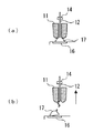
図3(a)は、本発明を適用することができる半導体装置の一例を示す断面図であり、図3(b)はその上面図である。ガラスエポキシ配線基板31上に、チップ32、スペーサチップ33、チップ34、チップ35が積載されている。また、チップ34,35上にはバンプ電極17が形成されている。そして、金ワイヤ12が、リード36にボールボンディングされ、バンプ電極17上にステッチボンディングされている。このように、チップ上に複数のバンプ電極を形成し、前記チップ上のバンプ電極にステッチボンディングによって接続する複数のワイヤを形成する半導体装置の製造方法に本発明を適用することができる。このような場合でも、やはり、何れかのチップ上に形成する全てのバンプ電極をまとめて形成した後で、そのチップに接続するワイヤを形成するのは好ましくなく、例えば、バンプ電極を1個形成するごとに、接続するワイヤを形成するか、もしくは、複数のバンプを形成する工程と、複数のワイヤを形成する工程を繰り返すようにするのが好ましい。図3の半導体装置においては、さらに、全体が樹脂37により封止され、ガラスエポキシ配線基板31の底面に半田ボール38が形成されている。
FIG. 3A is a cross-sectional view showing an example of a semiconductor device to which the present invention can be applied, and FIG. 3B is a top view thereof. A
図4(a)は、本発明を適用することができる半導体装置の他の例を示す断面図であり、図4(b)はその上面図である。ダイパッド41上にチップ42とチップ43が並べて搭載されている。このチップ42,43とリード44は金ワイヤ12により接続されている。また、チップ43のAlパッド上にはバンプ電極17が形成されている。そして、金ワイヤ12が、チップ42のAlパッドにボールボンディングされ、バンプ電極17上にステッチボンディングされている。このチップ間ボンディングに本発明を適用することができる。さらに、全体が樹脂45により封止されている。
4A is a cross-sectional view showing another example of a semiconductor device to which the present invention can be applied, and FIG. 4B is a top view thereof. A
実施の形態2.
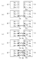
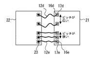
図5は、本発明の実施の形態2に係る半導体装置の製造方法を示す上面図である。まず、図5に示すように、複数のAlパッド16d(第1の複数のパッド)と、この複数のAlパッド16dよりも間隔が広い複数のAlパッド16e(第2の複数のパッド)とを有するチップ21(第1のチップ)と、複数のAlパッド23(第3の複数のパッド)を有するチップ22(第2のチップ)を準備する。
Embodiment 2. FIG.
FIG. 5 is a top view showing a method for manufacturing a semiconductor device according to the second embodiment of the present invention. First, as shown in FIG. 5, a plurality of
次に、キャピラリ11から排出した金ワイヤによって、チップ21の複数のAlパッド16dにそれぞれバンプ電極17d(第1の複数のバンプ電極)を形成し、複数のAlパッド16eにそれぞれバンプ電極17e(第2の複数のバンプ電極)を形成する。
Next,
その後、キャピラリから排出したワイヤによって、複数のバンプ電極17dと、複数のAlパッド23の何れかとを電気的に接続する金ワイヤ12d(第1の複数のワイヤ)を形成する。具体的には、キャピラリを用いてチップ22の複数のAlパッド23の一つに金ワイヤ12dの先端の金ボールをボールボンディングした後、対応するAlパッド16dのバンプ電極17d上に金ワイヤ12をステッチボンディングする。
Thereafter, a
その後、同様に、キャピラリから排出したワイヤによって、複数のバンプ電極17eと、複数のAlパッド23の別の何れかとを電気的に接続する金ワイヤ12e(第2の複数のワイヤ)を形成する。
Thereafter, similarly, the
このように、チップ21の複数のAlパッド16d,16eのうち、隣接するパッド間のピッチが広いパッド16dに接続するワイヤ12dの形成を、ピッチが狭いパッド16eへ接続するワイヤ12eの形成よりも先に行う。
As described above, among the plurality of
ここで、チップ21の複数のAlパッド16d,16eに、ステッチボンディングによりワイヤを接続する場合には、ステッチボンディング工程におけるチップへの局所的な応力集中を軽減するために、あらかじめ柔軟な金ボールからなるバンプ電極17d,17eをAlパッド16d,16e上に形成しておく。このとき、複数のバンプ電極1717d,17eを連続して形成すると、金ワイヤの消費量が少ないために、バンプ電極形成によって発生する金ワイヤのS字曲がりが、キャピラリ11内の特定のワイヤに繰り返し蓄積され、大きなS字曲がりが生じたワイヤdがキャピラリ11内に形成される。このように、大きなS字曲がりが生じたワイヤ12dを、ピッチが狭いパッド16eに接続するワイヤとして使用すると、ワイヤ同士の短絡の可能性が高まる。
Here, when wires are connected to the plurality of
そこで、本発明においては、連続するバンプ電極17d,17eの形成によって、大きなS字曲がりが蓄積されたワイヤ12dを、ピッチが広いパッド16dに接続するワイヤとして消費することで、ピッチが狭いパッド16eを接続するワイヤ12e同士の短絡の発生を防ぐことができる。
Therefore, in the present invention, by forming the
具体的には、ヨレが蓄積された金ワイヤを接続する対象である、ピッチが広いAlパッド16eについて、金ワイヤのループ長さに応じて最小ピッチを以下のようにするのが好ましい。

なお、本実施の形態2を実施の形態1と組み合わせることで、金ワイヤのS字曲がりを抑制することができ、金ワイヤ同士が電気的にショートするのを更に確実に防ぐことができる。 In addition, by combining the second embodiment with the first embodiment, it is possible to suppress the S-curve of the gold wire and further reliably prevent the gold wires from being electrically short-circuited.
実施の形態3.
図6(a)〜(d)は、本発明の実施の形態3に係る半導体装置の製造方法を示す断面図である。また、図7(a)〜(c)は、キャピラリの先端部を示す拡大断面図である。
Embodiment 3 FIG.
6A to 6D are cross-sectional views illustrating a method for manufacturing a semiconductor device according to the third embodiment of the present invention. FIGS. 7A to 7C are enlarged sectional views showing the tip of the capillary.
まず、図6(a)に示すように、キャピラリ11から排出した金ワイヤ12の先端の金ボールをチップ21のAlパッド16上に接合させてバンプ電極17を形成する。そして、図6(b)に示すように、キャピラリ11を15μm上昇させる。ここで、バンプ電極17の高さは15μmであるため、キャピラリ11はバンプ電極17よりも上に退避される。本実施の形態において使用するキャピラリ11及び金ワイヤ12の寸法は、図7(a)に示すように、キャピラリ11の内径が30μm、金ワイヤ12の直径が23μmである。
First, as shown in FIG. 6A, the gold ball at the tip of the
その後に、図6(c)に示すように、キャピラリ11を横方向に往復運動させる。ただし、キャピラリ11の動作振幅を少なくとも金ワイヤ12とキャピラリ11の内壁との隙間以上とする。具体的には、金ワイヤ12の直径が23μm、キャピラリ11の内径が30μmであるため、両者の隙間は平均すると片側で3.5μm、両側合わせると7μmである。動作振幅としては、最低限、キャピラリ11内壁と金ワイヤ12の片側の隙間である3.5μm以上である必要がある。金ワイヤ12のテールカット部分に十分なストレスを付与し、カット強度を低下させるためには、動作振幅としては、キャピラリ11内壁と金ワイヤ12の両側の隙間の和である7μm以上にするのがより好ましい。そこで、例えば図面7(b)に示すように、キャピラリ11を一方向へ30μm水平移動させた後、図面7(c)に示すように、反対方向に65μm水平移動させる。これにより、金ワイヤ12のテールカット部分にストレスを付与し、カット強度を低減させることができる。また、水平移動の大きさによっては、水平移動によって、金ワイヤ12をバンプ電極17から切断する事も可能である。
Thereafter, as shown in FIG. 6C, the capillary 11 is reciprocated in the lateral direction. However, the operation amplitude of the capillary 11 is set to be at least the gap between the
その後に、図6(d)に示すように、クランパ14で金ワイヤ12を挟んで上方向に引っ張ることで金ワイヤ12をカットする。この際、キャピラリ11の往復運動により金ワイヤ12の強度を低減しているため、金ワイヤ12のカットの反動を低減することができ、金ワイヤ12のS字曲がり及びバンプ電極17の剥がれを抑制することができる。
After that, as shown in FIG. 6D, the
また、キャピラリ11の往復運動の前にキャピラリ11をバンプ電極17よりも上に退避することで、往復運動の際にキャピラリ11とバンプ電極17が接触してバンプ電極17がダメージを受けるのを防ぐことができる。
Further, by retracting the capillary 11 above the
なお、キャピラリ11を横方向へ往復運動させる代わりに横方向へ円運動させてもよく、その他、ベクトルで分解した場合に横方向への移動を含む動作であればよい。また、振動の周波数や動作手段については、特に限定する物ではないが、超音波振動の振幅は一般的に1μm以下であるため、金ワイヤ12の強度を低減させるためのキャピラリ11の動作として十分な振幅を得るのは難しい。本実施の形態においては、モーターを動力源として、機械的に位置制御しながら動作させることによって、上記キャピラリ11の水平移動動作を発生させた。また、本実施の形態3も図2又は図3の半導体装置に適用することができる。
Instead of reciprocating the capillary 11 in the horizontal direction, the capillary 11 may be circularly moved in the horizontal direction, or any other operation that includes movement in the horizontal direction when decomposed by a vector may be used. Further, the vibration frequency and operation means are not particularly limited. However, since the amplitude of ultrasonic vibration is generally 1 μm or less, the operation of the capillary 11 for reducing the strength of the
実施の形態4.
図8(a)〜(d)は、本発明の実施の形態4に係る半導体装置の製造方法を示す断面図である。
Embodiment 4 FIG.
8A to 8D are cross-sectional views illustrating a method for manufacturing a semiconductor device according to the fourth embodiment of the present invention.
まず、図8(a)に示すように、キャピラリ11を用いて、チップ22のAlパッド23に金ワイヤ12先端の金ボールをボールボンディングした後、チップ21のAlパッド16上に形成されたバンプ電極17上に金ワイヤ12をステッチボンディングする。具体的には、キャピラリ11により金ワイヤ12をバンプ電極17に10ms間押圧し、超音波振動をかけて金ワイヤ12を潰してバンプ電極17に接合する。
First, as shown in FIG. 8A, a bump formed on the
その後に、図8(b)に示すように、キャピラリ11を金ワイヤ12のループ進入方向に、後工程のキャピラリ11の横方向動作の振幅の半分以上退避させる。例えば、キャピラリ11を30μm水平移動させる。
After that, as shown in FIG. 8B, the capillary 11 is retracted in the loop approach direction of the
その後に、図8(c)に示すように、実施の形態3と同様に、キャピラリ11を横方向に往復運動させる。ただし、キャピラリ11の動作振幅を少なくとも金ワイヤ12とキャピラリ11の内壁との隙間以上とする。すなわち、動作振幅としては、最低限、キャピラリ11内壁と金ワイヤ12の片側の隙間である3.5μm以上である必要がある。また、金ワイヤ12のテールカット部分に十分なストレスを付与し、カット強度を低下させるためには、動作振幅としては、キャピラリ11内壁と金ワイヤ12の両側の隙間の和である7μm以上にするのがより好ましい。本実施の形態における動作振幅は40μmである。
Thereafter, as shown in FIG. 8C, the capillary 11 is reciprocated in the lateral direction as in the third embodiment. However, the operation amplitude of the capillary 11 is set to be at least the gap between the
その後に、図8(d)に示すように、クランパ14で金ワイヤ12を挟んで上方向に引っ張ることで金ワイヤ12をカットする。この際、キャピラリ11の往復運動により金ワイヤ12のカット強度を低減しているため、金ワイヤ12のカットの反動を低減することができ、金ワイヤ12のS字曲がり及びバンプ電極17の剥がれを抑制することができる。往復運動の動作振幅によっては、往復運動によって金ワイヤ12を切断する事も可能である。この場合には、金ワイヤ12のカットの反動によるワイヤのS字曲がりは最小限に抑える事ができる。
Thereafter, as shown in FIG. 8D, the
また、キャピラリ11の往復運動の前に、ステッチボンディングを開始した位置、すなわち、金ワイヤ12がバンプ電極17に接触した位置からキャピラリ11を往復動作の振幅の半分以上離しているため、キャピラリ11の往復運動において、金ワイヤ12とバンプ電極17との接合部分や、金ワイヤ12の根本の部分へのストレスの付与を軽減する事ができ、ワイヤの大幅な強度の低下や、断線を防ぐことができる。
Further, since the capillary 11 is separated from the position where the stitch bonding is started, that is, the position where the
11 キャピラリ
12、12a〜12e 金ワイヤ(ワイヤ)
16、16a〜16e、23、23a〜23c Alパッド(パッド)
17、17a〜17e バンプ電極
21、22 チップ
11
16, 16a-16e, 23, 23a-23c Al pad (pad)
17, 17a-
Claims (9)
キャピラリから排出したワイヤによって、前記第1の複数のパッドの何れかに、第1のバンプ電極を形成する工程と、
前記第1のバンプ電極を形成する工程の後に、前記キャピラリから排出したワイヤによって、前記第1のバンプ電極と、前記第2の複数のパッドの何れかとを電気的に接続する第1のワイヤを形成する工程と、
前記第1のワイヤを形成する工程の後に、前記キャピラリから排出したワイヤによって、前記第1の複数のパッドの別の何れかに、第2のバンプ電極を形成する工程とを有する半導体装置の製造方法。 Providing a first chip having a first plurality of pads and a second chip having a second plurality of pads;
Forming a first bump electrode on any of the first plurality of pads with a wire discharged from the capillary;
After the step of forming the first bump electrode, a first wire that electrically connects the first bump electrode and any of the second plurality of pads with a wire discharged from the capillary Forming, and
After the step of forming the first wire, a step of forming a second bump electrode on any one of the first plurality of pads with the wire discharged from the capillary Method.
キャピラリから排出したワイヤによって、前記第1の複数のパッド上に、第1の複数のバンプ電極を形成し、前記第2の複数のパッド上に、第2の複数のバンプ電極を形成する工程と、
前記第1及び第2の複数のバンプ電極を形成する工程の後に、前記キャピラリから排出したワイヤによって、前記第1の複数のバンプ電極と、前記第3の複数のパッドの何れかとを電気的に接続する第1の複数のワイヤを形成する工程と、
前記第1の複数のワイヤを形成する工程の後に、前記キャピラリから排出したワイヤによって、前記第2の複数のバンプ電極と、前記第3の複数のパッドの別の何れかとを電気的に接続する第2の複数のワイヤを形成する工程とを有する半導体装置の製造方法。 A first chip having a first plurality of pads, a second plurality of pads having a smaller interval than the first plurality of pads, and a second chip having a third plurality of pads are prepared. Process,
Forming a first plurality of bump electrodes on the first plurality of pads and forming a second plurality of bump electrodes on the second plurality of pads by wires discharged from the capillaries; ,
After the step of forming the first and second plurality of bump electrodes, the first plurality of bump electrodes and any of the third plurality of pads are electrically connected by a wire discharged from the capillary. Forming a first plurality of wires to be connected;
After the step of forming the first plurality of wires, the second plurality of bump electrodes and another one of the third plurality of pads are electrically connected by the wire discharged from the capillary. Forming a second plurality of wires.
前記バンプ電極を形成する工程の後に、少なくとも前記ワイヤと前記キャピラリの内壁との隙間以上の振幅で前記キャピラリを横方向に動作させる工程と、
前記キャピラリを横方向に動作させる工程の後に、クランパで前記ワイヤを挟んで上方向に引っ張ることで前記ワイヤをカットする工程とを有することを特徴とする半導体装置の製造方法。 Forming a bump electrode on the pad with a wire passed through the capillary;
After the step of forming the bump electrode, the step of operating the capillary in the lateral direction with an amplitude of at least the gap between the wire and the inner wall of the capillary;
And a step of cutting the wire by pulling the wire upward by sandwiching the wire with a clamper after the step of operating the capillary laterally.
前記ステッチボンディングする工程の後に、少なくとも前記ワイヤと前記キャピラリの内壁との隙間以上の振幅で前記キャピラリを横方向に動作させる工程と、
前記キャピラリを横方向に動作させる工程の後に、クランパで前記ワイヤを挟んで上方向に引っ張ることで前記ワイヤをカットする工程とを有することを特徴とする半導体装置の製造方法。 A step of stitch bonding a wire on the bump electrode using a capillary;
After the step of stitch bonding, the step of operating the capillary laterally with an amplitude that is at least greater than the gap between the wire and the inner wall of the capillary;
And a step of cutting the wire by pulling the wire upward by sandwiching the wire with a clamper after the step of operating the capillary laterally.
Priority Applications (2)
| Application Number | Priority Date | Filing Date | Title |
|---|---|---|---|
| JP2005091023A JP2006278407A (en) | 2005-03-28 | 2005-03-28 | Manufacturing method of semiconductor device |
| US11/347,231 US20060216863A1 (en) | 2005-03-28 | 2006-02-06 | Method of manufacturing semiconductor device |
Applications Claiming Priority (1)
| Application Number | Priority Date | Filing Date | Title |
|---|---|---|---|
| JP2005091023A JP2006278407A (en) | 2005-03-28 | 2005-03-28 | Manufacturing method of semiconductor device |
Publications (2)
| Publication Number | Publication Date |
|---|---|
| JP2006278407A true JP2006278407A (en) | 2006-10-12 |
| JP2006278407A5 JP2006278407A5 (en) | 2008-05-15 |
Family
ID=37035733
Family Applications (1)
| Application Number | Title | Priority Date | Filing Date |
|---|---|---|---|
| JP2005091023A Pending JP2006278407A (en) | 2005-03-28 | 2005-03-28 | Manufacturing method of semiconductor device |
Country Status (2)
| Country | Link |
|---|---|
| US (1) | US20060216863A1 (en) |
| JP (1) | JP2006278407A (en) |
Cited By (3)
| Publication number | Priority date | Publication date | Assignee | Title |
|---|---|---|---|---|
| JP2007294581A (en) * | 2006-04-24 | 2007-11-08 | Shinkawa Ltd | Tail wire cutting method and program of bonding apparatus |
| US10804238B2 (en) | 2017-02-22 | 2020-10-13 | Murata Manufacturing Co., Ltd. | Semiconductor device having an electrical connection between semiconductor chips established by wire bonding, and method for manufacturing the same |
| WO2022013955A1 (en) * | 2020-07-15 | 2022-01-20 | 株式会社新川 | Wire bonding device, and semiconductor device manufacturing method |
Families Citing this family (10)
| Publication number | Priority date | Publication date | Assignee | Title |
|---|---|---|---|---|
| US20100320592A1 (en) * | 2006-12-29 | 2010-12-23 | Sanyo Electric Co., Ltd. | Semiconductor device and method for manufacturing the same |
| JP2009158750A (en) * | 2007-12-27 | 2009-07-16 | Fujifilm Corp | Wire bonding method and semiconductor device |
| EP2133915A1 (en) * | 2008-06-09 | 2009-12-16 | Micronas GmbH | Semiconductor assembly with specially formed bonds and method for manufacturing the same |
| MY152355A (en) * | 2011-04-11 | 2014-09-15 | Carsem M Sdn Bhd | Short and low loop wire bonding |
| MY181180A (en) * | 2011-09-09 | 2020-12-21 | Carsem M Sdn Bhd | Low loop wire bonding |
| US9093515B2 (en) * | 2013-07-17 | 2015-07-28 | Freescale Semiconductor, Inc. | Wire bonding capillary with working tip protrusion |
| US9087815B2 (en) * | 2013-11-12 | 2015-07-21 | Invensas Corporation | Off substrate kinking of bond wire |
| US9082753B2 (en) * | 2013-11-12 | 2015-07-14 | Invensas Corporation | Severing bond wire by kinking and twisting |
| JP5686912B1 (en) * | 2014-02-20 | 2015-03-18 | 株式会社新川 | Bump forming method, bump forming apparatus, and semiconductor device manufacturing method |
| WO2018152647A1 (en) * | 2017-02-24 | 2018-08-30 | Reflex Photonics Inc. | Wirebonding for side-packaged optical engine |
Citations (5)
| Publication number | Priority date | Publication date | Assignee | Title |
|---|---|---|---|---|
| JPH10303201A (en) * | 1997-02-28 | 1998-11-13 | Sony Corp | Capillary, its use method and bump formation device |
| JP2001118877A (en) * | 1999-10-19 | 2001-04-27 | Fujitsu Ltd | Semiconductor device and manufacturing method therefor |
| JP2003059961A (en) * | 2001-08-16 | 2003-02-28 | Mitsubishi Electric Corp | Wire-bonding method and semiconductor device |
| JP2004056021A (en) * | 2002-07-23 | 2004-02-19 | Sharp Takaya Denshi Kogyo Kk | Wire bonding method |
| JP2004356382A (en) * | 2003-05-29 | 2004-12-16 | Renesas Technology Corp | Semiconductor integrated circuit device |
Family Cites Families (3)
| Publication number | Priority date | Publication date | Assignee | Title |
|---|---|---|---|---|
| JPH09312375A (en) * | 1996-03-18 | 1997-12-02 | Hitachi Ltd | Lead frame, semiconductor device and manufacture thereof |
| JP3913134B2 (en) * | 2002-08-08 | 2007-05-09 | 株式会社カイジョー | Bump forming method and bump |
| US7229906B2 (en) * | 2002-09-19 | 2007-06-12 | Kulicke And Soffa Industries, Inc. | Method and apparatus for forming bumps for semiconductor interconnections using a wire bonding machine |
-
2005
- 2005-03-28 JP JP2005091023A patent/JP2006278407A/en active Pending
-
2006
- 2006-02-06 US US11/347,231 patent/US20060216863A1/en not_active Abandoned
Patent Citations (5)
| Publication number | Priority date | Publication date | Assignee | Title |
|---|---|---|---|---|
| JPH10303201A (en) * | 1997-02-28 | 1998-11-13 | Sony Corp | Capillary, its use method and bump formation device |
| JP2001118877A (en) * | 1999-10-19 | 2001-04-27 | Fujitsu Ltd | Semiconductor device and manufacturing method therefor |
| JP2003059961A (en) * | 2001-08-16 | 2003-02-28 | Mitsubishi Electric Corp | Wire-bonding method and semiconductor device |
| JP2004056021A (en) * | 2002-07-23 | 2004-02-19 | Sharp Takaya Denshi Kogyo Kk | Wire bonding method |
| JP2004356382A (en) * | 2003-05-29 | 2004-12-16 | Renesas Technology Corp | Semiconductor integrated circuit device |
Cited By (9)
| Publication number | Priority date | Publication date | Assignee | Title |
|---|---|---|---|---|
| JP2007294581A (en) * | 2006-04-24 | 2007-11-08 | Shinkawa Ltd | Tail wire cutting method and program of bonding apparatus |
| JP4679427B2 (en) * | 2006-04-24 | 2011-04-27 | 株式会社新川 | Tail wire cutting method and program for bonding apparatus |
| US10804238B2 (en) | 2017-02-22 | 2020-10-13 | Murata Manufacturing Co., Ltd. | Semiconductor device having an electrical connection between semiconductor chips established by wire bonding, and method for manufacturing the same |
| US11417625B2 (en) | 2017-02-22 | 2022-08-16 | Murata Manufacturing Co., Ltd. | Semiconductor device having an electrical connection between semiconductor chips established by wire bonding, and method for manufacturing the same |
| WO2022013955A1 (en) * | 2020-07-15 | 2022-01-20 | 株式会社新川 | Wire bonding device, and semiconductor device manufacturing method |
| JPWO2022013955A1 (en) * | 2020-07-15 | 2022-01-20 | ||
| KR20220009937A (en) * | 2020-07-15 | 2022-01-25 | 가부시키가이샤 신가와 | Wire bonding device and semiconductor device manufacturing method |
| JP7152079B2 (en) | 2020-07-15 | 2022-10-12 | 株式会社新川 | Wire bonding apparatus and method for manufacturing semiconductor device |
| KR102488240B1 (en) | 2020-07-15 | 2023-01-13 | 가부시키가이샤 신가와 | Wire bonding device and semiconductor device manufacturing method |
Also Published As
| Publication number | Publication date |
|---|---|
| US20060216863A1 (en) | 2006-09-28 |
Similar Documents
| Publication | Publication Date | Title |
|---|---|---|
| JP2006278407A (en) | Manufacturing method of semiconductor device | |
| US7176570B2 (en) | Method for forming bump, semiconductor element having bumps and method of manufacturing the same, semiconductor device and method of manufacturing the same, circuit board, and electronic equipment | |
| JP4860128B2 (en) | Wire bonding method | |
| US7314818B2 (en) | Semiconductor device and method of manufacturing the same, circuit board, and electronic equipment | |
| JP2006324553A (en) | Semiconductor device and method of manufacturing same | |
| US7044357B2 (en) | Bump formation method and wire bonding method | |
| US6921016B2 (en) | Semiconductor device and method of manufacturing the same, circuit board, and electronic equipment | |
| JP5714195B2 (en) | Manufacturing method of semiconductor device | |
| JP2008034567A (en) | Semiconductor device and manufacturing method therefor | |
| JP2008277751A (en) | Method of manufacturing semiconductor device, and semiconductor device | |
| JP2009259981A (en) | Semiconductor device, and method of manufacturing the same | |
| JP2008066331A (en) | Manufacturing method of semiconductor device | |
| US7629688B2 (en) | Bonded structure and bonding method | |
| JP2010123817A (en) | Wire bonding method, electronic apparatus, and method of manufacturing the same | |
| JP4385878B2 (en) | Implementation method | |
| JP4041045B2 (en) | Ultrasonic flip chip bonding method | |
| JP2007266062A (en) | Process for manufacturing semiconductor device | |
| JP2010073747A (en) | Wire bonding method and semiconductor device | |
| JP5048990B2 (en) | Semiconductor device and manufacturing method thereof | |
| JP2008085094A (en) | Manufacturing method of semiconductor device | |
| JP2004207291A (en) | Semiconductor device and its manufacturing method, circuit board, and electronic equipment | |
| JP2000068316A (en) | Integrated circuit device | |
| JP2006108408A (en) | Semiconductor device and manufacturing method therefor | |
| JP2020178000A (en) | Optical module and manufacturing method thereof | |
| KR20070062084A (en) | Bump reverse stitch bonding method, chip stack structure and method using the same |
Legal Events
| Date | Code | Title | Description |
|---|---|---|---|
| A521 | Written amendment |
Free format text: JAPANESE INTERMEDIATE CODE: A523 Effective date: 20080326 |
|
| A621 | Written request for application examination |
Free format text: JAPANESE INTERMEDIATE CODE: A621 Effective date: 20080326 |
|
| A711 | Notification of change in applicant |
Free format text: JAPANESE INTERMEDIATE CODE: A712 Effective date: 20100521 |
|
| A977 | Report on retrieval |
Free format text: JAPANESE INTERMEDIATE CODE: A971007 Effective date: 20100827 |
|
| A131 | Notification of reasons for refusal |
Free format text: JAPANESE INTERMEDIATE CODE: A131 Effective date: 20100831 |
|
| A02 | Decision of refusal |
Free format text: JAPANESE INTERMEDIATE CODE: A02 Effective date: 20110104 |