JP2006269497A - Substrate-treating device and substrate storage method - Google Patents
Substrate-treating device and substrate storage method Download PDFInfo
- Publication number
- JP2006269497A JP2006269497A JP2005081607A JP2005081607A JP2006269497A JP 2006269497 A JP2006269497 A JP 2006269497A JP 2005081607 A JP2005081607 A JP 2005081607A JP 2005081607 A JP2005081607 A JP 2005081607A JP 2006269497 A JP2006269497 A JP 2006269497A
- Authority
- JP
- Japan
- Prior art keywords
- substrate
- wafer
- semiconductor wafer
- unit
- processing apparatus
- Prior art date
- Legal status (The legal status is an assumption and is not a legal conclusion. Google has not performed a legal analysis and makes no representation as to the accuracy of the status listed.)
- Withdrawn
Links
Images


Classifications
-
- H—ELECTRICITY
- H01—ELECTRIC ELEMENTS
- H01L—SEMICONDUCTOR DEVICES NOT COVERED BY CLASS H10
- H01L21/00—Processes or apparatus adapted for the manufacture or treatment of semiconductor or solid state devices or of parts thereof
- H01L21/67—Apparatus specially adapted for handling semiconductor or electric solid state devices during manufacture or treatment thereof; Apparatus specially adapted for handling wafers during manufacture or treatment of semiconductor or electric solid state devices or components ; Apparatus not specifically provided for elsewhere
- H01L21/68—Apparatus specially adapted for handling semiconductor or electric solid state devices during manufacture or treatment thereof; Apparatus specially adapted for handling wafers during manufacture or treatment of semiconductor or electric solid state devices or components ; Apparatus not specifically provided for elsewhere for positioning, orientation or alignment
- H01L21/681—Apparatus specially adapted for handling semiconductor or electric solid state devices during manufacture or treatment thereof; Apparatus specially adapted for handling wafers during manufacture or treatment of semiconductor or electric solid state devices or components ; Apparatus not specifically provided for elsewhere for positioning, orientation or alignment using optical controlling means
-
- Y—GENERAL TAGGING OF NEW TECHNOLOGICAL DEVELOPMENTS; GENERAL TAGGING OF CROSS-SECTIONAL TECHNOLOGIES SPANNING OVER SEVERAL SECTIONS OF THE IPC; TECHNICAL SUBJECTS COVERED BY FORMER USPC CROSS-REFERENCE ART COLLECTIONS [XRACs] AND DIGESTS
- Y10—TECHNICAL SUBJECTS COVERED BY FORMER USPC
- Y10S—TECHNICAL SUBJECTS COVERED BY FORMER USPC CROSS-REFERENCE ART COLLECTIONS [XRACs] AND DIGESTS
- Y10S414/00—Material or article handling
- Y10S414/135—Associated with semiconductor wafer handling
Landscapes
- Engineering & Computer Science (AREA)
- Physics & Mathematics (AREA)
- Condensed Matter Physics & Semiconductors (AREA)
- General Physics & Mathematics (AREA)
- Manufacturing & Machinery (AREA)
- Computer Hardware Design (AREA)
- Microelectronics & Electronic Packaging (AREA)
- Power Engineering (AREA)
- Container, Conveyance, Adherence, Positioning, Of Wafer (AREA)
- Testing Or Measuring Of Semiconductors Or The Like (AREA)
- Exposure Of Semiconductors, Excluding Electron Or Ion Beam Exposure (AREA)
Abstract
Description
この発明は、例えば基板検査装置や基板製造装置等の基板処理装置及び基板収納方法に関する。 The present invention relates to a substrate processing apparatus such as a substrate inspection apparatus and a substrate manufacturing apparatus, and a substrate storage method.
一般に、半導体ウエハ(基板)の外観を検査する場合には、カセットに収納された半導体ウエハを搬送ロボットにより取り出して、ミクロ検査部に搬送する前にミクロ検査部でアライメントが可能な程度にプリアライメントする。プリアライメントされた半導体ウエハは、ミクロ検査部でプリアライメントよりも精度の高いアライメント補正をおこなうことで正確な位置に配され、その後にミクロ検査がおこなわれる。このミクロ検査終了後には、半導体ウエハが搬送ロボットにより再びカセットに収納される(例えば、特許文献1参照。)。 In general, when inspecting the appearance of a semiconductor wafer (substrate), the semiconductor wafer stored in the cassette is taken out by a transfer robot and pre-aligned to the extent that alignment can be performed by the micro inspection unit before being transferred to the micro inspection unit. To do. The pre-aligned semiconductor wafer is arranged at an accurate position by performing alignment correction with higher accuracy than the pre-alignment in the micro-inspection unit, and then micro-inspection is performed. After the micro inspection is completed, the semiconductor wafer is again stored in the cassette by the transfer robot (see, for example, Patent Document 1).
すなわち、カセットから取り出された半導体ウエハを検査装置に搬入した際に、半導体ウエハの中心が1〜2mmずれてしまうと、ミクロ検査部でのアライメントが不能となる場合があるため、このミクロ検査部でのアライメントを確実に行うことができるように、前述のプリアライメント補正がなされる。
また、この半導体ウエハは、ミクロ検査部の受け渡し位置にて待機している回転ステージに受け渡され、ミクロ検査部において、プリアライメントよりも精度の高いアライメント補正及びミクロ検査が行われる。ミクロ検査が終了すると、回転ステージは待機位置に復帰し、搬送ロボットにより半導体ウエハがカセットに収納される。
The semiconductor wafer is transferred to a rotating stage waiting at a transfer position of the micro inspection unit, and alignment correction and micro inspection with higher accuracy than pre-alignment are performed in the micro inspection unit. When the micro inspection is completed, the rotary stage returns to the standby position, and the semiconductor wafer is stored in the cassette by the transfer robot.
以上のように、ミクロ検査に先立って精度の高いアライメントが行われているが、ミクロ検査が終了した後には、半導体ウエハを載置した回転ステージが、アライメント前の待機位置に自動的に復帰するため、半導体ウエハの中心がずれた状態で搬送ロボットに受け渡される。さらに、半導体ウエハが搬送ロボットに受け渡される際に、搬送ロボットに対する半導体ウエハの位置にずれが生じることで、カセット内の適正な位置に半導体ウエハを戻せない虞がある。特に、半導体ウエハをカセットに収納する際に、半導体ウエハがカセットの内壁面に衝突すると半導体ウエハが傷ついたり、ゴミが発生したりするという問題がある。 As described above, high-precision alignment is performed prior to the micro inspection, but after the micro inspection is completed, the rotary stage on which the semiconductor wafer is placed automatically returns to the standby position before alignment. Therefore, the semiconductor wafer is transferred to the transfer robot with the center being shifted. Further, when the semiconductor wafer is transferred to the transfer robot, the position of the semiconductor wafer with respect to the transfer robot may be shifted, and the semiconductor wafer may not be returned to an appropriate position in the cassette. In particular, when the semiconductor wafer is stored in the cassette, there is a problem that the semiconductor wafer is damaged or dust is generated if the semiconductor wafer collides with the inner wall surface of the cassette.
この発明は上述した事情に鑑みてなされたものであって、基板をカセット内に正確に戻し、基板の損傷やゴミの発生を防止できる基板処理装置及び基板収納方法を提供することを目的としている。 The present invention has been made in view of the above-described circumstances, and an object thereof is to provide a substrate processing apparatus and a substrate storage method capable of accurately returning a substrate into a cassette and preventing damage to the substrate and generation of dust. .
上記目的を達成するために、この発明は、以下の手段を提供する。
本発明は、収納体から取り出された基板を搬送手段により処理装置本体に搬送する工程と、該処理装置本体において前記基板の適宜処理を行う工程と、適宜処理を行った前記基板を前記搬送手段により前記収納体に戻す工程とを備える基板処理装置の基板収納方法において、前記基板を前記搬送手段から前記処理装置本体に受け渡す工程から、前記基板を前記収納体に戻す工程の前までに、前記搬送手段における前記基板の正規位置に対する前記基板のずれ量を算出する工程と、前記処理装置本体において前記基板の適宜処理を行う工程の後から、前記基板を前記収納体に戻す工程までの間に、算出された前記ずれ量に基づいて前記収納体への前記基板の戻し位置を補正する工程とを備えることを特徴とする基板処理装置の基板収納方法を提供する。
なお、処理装置本体における基板の処理とは、例えば、基板の製造や検査処理のことを示している。
In order to achieve the above object, the present invention provides the following means.
The present invention includes a step of transporting a substrate taken out from a storage body to a processing apparatus main body by a transporting means, a step of appropriately processing the substrate in the processing apparatus main body, and the substrate subjected to appropriate processing to the transporting means. In the substrate storage method of the substrate processing apparatus comprising the step of returning the substrate to the storage body, from the step of transferring the substrate from the transport means to the processing apparatus body, and before the step of returning the substrate to the storage body, After the step of calculating the amount of deviation of the substrate with respect to the normal position of the substrate in the transport means and the step of appropriately processing the substrate in the processing apparatus main body, and the step of returning the substrate to the container And a step of correcting the return position of the substrate to the storage body based on the calculated shift amount. To.
In addition, the process of the board | substrate in a processing apparatus main body has shown the manufacture and test | inspection process of a board | substrate, for example.
また、本発明は、収納体から取り出した基板に適宜処理を施す処理装置本体と、前記処理装置本体から前記基板を収納する収納体に前記基板を搬送する搬送手段と、前記搬送手段における前記基板の正規位置に対する前記基板のずれ量を算出するずれ量算出手段と、前記ずれ量算出手段において算出された前記ずれ量に基づいて、前記収納体への前記基板の戻し位置を補正するずれ量補正手段とを備えることを特徴とする基板処理装置を提供する。 In addition, the present invention provides a processing apparatus main body for appropriately processing a substrate taken out from a storage body, a transfer means for transferring the substrate from the processing apparatus main body to a storage body for storing the substrate, and the substrate in the transfer means. A deviation amount calculating means for calculating a deviation amount of the substrate with respect to the normal position, and a deviation amount correction for correcting a return position of the substrate to the storage body based on the deviation amount calculated by the deviation amount calculating means. And a substrate processing apparatus.
本発明の基板処理装置の基板収納方法によれば、基板を収納体に戻すまでの間に、基板のずれ量に基づいて収納体への基板の戻し位置を補正するため、基板を収納体に戻す際には、基板を収納体の規定位置に配することができる。したがって、基板が収納体の壁部に衝突することを防止して、基板の損傷やゴミの発生を防ぐことができる。
特に、処理装置本体から搬送手段に基板を受け渡す工程において、算出したずれ量に基づいて基板を搬送手段の正規位置に配する場合には、搬送手段の正規位置及び収納体の規定位置の相対的な位置関係を基準として、基板を確実に収納体の規定位置に配することができる。
According to the substrate storage method of the substrate processing apparatus of the present invention, the substrate is stored in the storage body in order to correct the return position of the substrate to the storage body based on the displacement amount of the substrate until the substrate is returned to the storage body. When returning, the substrate can be placed at a specified position of the housing. Therefore, it is possible to prevent the substrate from colliding with the wall portion of the storage body, thereby preventing the substrate from being damaged or generating dust.
In particular, in the step of transferring the substrate from the processing apparatus main body to the transport unit, when the substrate is arranged at the normal position of the transport unit based on the calculated deviation amount, the relative position between the normal position of the transport unit and the specified position of the storage body The substrate can be surely arranged at the specified position of the storage body with reference to the specific positional relationship.
また、本発明の基板処理装置によれば、基板を処理装置本体から収納体に搬送する際には、基板が搬送手段の正規位置に対してずれていても、ずれ量算出手段において求められたずれ量に基づいてずれ量補正手段により収納体への基板の戻し位置を補正する。このため、基板を収納体に戻す際には、基板を収納体における基板の規定位置に配することができる。 Further, according to the substrate processing apparatus of the present invention, when the substrate is transported from the processing apparatus main body to the storage body, even if the substrate is deviated from the normal position of the transport means, it is obtained by the displacement amount calculating means. Based on the shift amount, the shift amount correcting means corrects the return position of the substrate to the storage body. For this reason, when returning a board | substrate to a storage body, a board | substrate can be distribute | arranged to the regulation position of the board | substrate in a storage body.
以下、図面を参照して本発明による第1の実施形態について図1,2を参照して詳細に説明する。
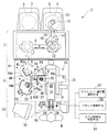
図1に示すように、本発明の基板収納方法に係る基板検査装置(基板処理装置)1は、デバイスパターンを形成した半導体ウエハ(基板)Sの表裏面の欠陥検査処理を行うものである。この基板検査装置1にはウエハカセット(収納体)3が配されており、このウエハカセット3内には複数の半導体ウエハSが上下方向に所定ピッチで収納されている。この基板検査装置1は、半導体ウエハSの検査を行う検査部5と、ウエハカセット3と検査部5との間で半導体ウエハSを搬送するローダ部(第2の搬送部)7とを備えている。
Hereinafter, a first embodiment of the present invention will be described in detail with reference to FIGS.
As shown in FIG. 1, a substrate inspection apparatus (substrate processing apparatus) 1 according to a substrate storage method of the present invention performs a defect inspection process on the front and back surfaces of a semiconductor wafer (substrate) S on which a device pattern is formed. The
ローダ部7は、複数(図示例では2つ)のウエハカセット3を着脱可能に取り付けられるように構成されており、これらのウエハカセット3の間をシフト機構9により往復移動するウエハ搬送ロボット11を備えている。シフト機構9は、各ウエハカセット3との間で半導体ウエハSの受け渡しを行う位置と、検査部5との間で半導体ウエハSの受け渡しを行う位置との間で、ウエハ搬送ロボット11を一方向(C方向)に往復移動させるものである。
ウエハ搬送ロボット11は、所謂多関節型のロボットであり、回転軸13と、半導体ウエハSを載置する板状の載置板15と、これら回転軸13及び載置板15を相互に連結する3つの連結アーム17〜19とを備えている。
The
The
すなわち、第1の連結アーム17の一端は、回転軸13に対して回転自在に連結されており、第1の連結アーム17の他端は、第2の連結アーム18の一端との間で互いに回転自在に連結されている。第2の連結アーム18の他端は、第3の連結アーム19の一端との間で互いに回転自在に連結されており、第3の連結アーム19の他端に載置板15が固定されている。したがって、これら3つの連結アーム17〜19を適宜回転させることにより、回転軸13から載置板15までの距離が変化することになる、すなわち、ウエハ搬送ロボット11の伸縮動作が行われることになる。
That is, one end of the first connecting
載置板15の表面には、複数の吸着孔21が形成されており、これら吸着孔21は、図示しない吸引ポンプ(図示せず)に連通されている。すなわち、載置板15の表面に半導体ウエハSを載置した状態において吸引ポンプを動作させた際には、半導体ウエハSが吸引ポンプの吸引力により載置板15に吸着することになる。
ローダ部7は、以上のように構成されているため、載置板15を各ウエハカセット3内と検査部5内のウエハ搬入位置P1との間で移動させることができる。なお、ウエハ搬入位置P1は、ウエハ搬送ロボット11と検査部5との間で半導体ウエハSの受け渡しを行う位置を示している。
A plurality of
Since the
検査部5は、周知のマクロ検査部23及びミクロ検査部(処理装置本体)25と、検査部5のウエハ搬入位置P1、マクロ検査部23及びミクロ検査部25の間で半導体ウエハSを搬送する回転搬送部(第1の搬送部)27とを備えている。
ミクロ検査部25は、回転搬送部27とのウエハ受け渡し位置P3に設けられたアライメント用の位置検出センサ29と、半導体ウエハSの像を拡大する顕微鏡31と、半導体ウエハSを載置すると共に回転機構を有するウエハ保持部33と、ウエハ受け渡し位置P3と顕微鏡31の所定の観察位置との間でウエハ保持部33を移動させるXYステージ35とを備えている。
The
The
位置検出センサ29は、例えば、CCDカメラから構成されており、回転搬送部27とのウエハ受け渡し位置P3において、半導体ウエハSが回転搬送部27からウエハ保持部33に受け渡された後に、ウエハ保持部33を回転させて半導体ウエハSのエッジ位置を画像から検出するものである。この検出結果は、ウエハ保持部33における半導体ウエハSの正規位置に対する半導体ウエハSの中心ずれを及び角度ずれの補正に使用するものである。
このミクロ検査部25においては、顕微鏡31で拡大された半導体ウエハSの像をCCDカメラ等の撮像装置37により撮像したり、接眼レンズ39を通して観察できるようになっている。
The
In the
回転搬送部27は、回転軸41を中心(図示例では、左回り)に回転するものであり、回転軸41からその直交方向に延出する3つの回転アーム43a〜43cを備えている。これら3つの回転アーム43a〜43cは、回転軸41回りに等角度(例えば、120度毎)に配されている。また、これら3つの回転アーム43a〜43cは、ウエハ搬送ロボット11との受け渡しを行うウエハ搬入位置P1、マクロ検査部23によりマクロ検査を行うマクロ検査位置P2、及び、ミクロ検査部25とのウエハ受け渡し位置P3の間を回転循環する。
The
各回転アーム43a〜43cの先端には、半導体ウエハSを載置する略L字状のハンド44a〜44cが設けられている。ハンド44a〜44cの表面には、複数の吸着孔が形成されており、これら吸着孔は、図示しない吸引ポンプ(図示せず)に連通されている。すなわち、ハンド44a〜44cの表面に半導体ウエハSを載置した状態において吸引ポンプを動作させた際には、半導体ウエハSが吸引ポンプの吸引力によりハンド44a〜44cに吸着することになる。
この回転搬送部27とローダ部7のシフト機構9及びウエハ搬送ロボット11とにより半導体ウエハSを搬送する搬送手段が構成されている。
At the tips of the rotating arms 43a to 43c, substantially L-
The
ウエハ搬入位置P1には、半導体ウエハSのプリアライメント用の位置検出センサ45〜48が複数(図示例では4つ)設けられている。これら位置検出センサ45〜48は、例えば、ラインセンサ又は二次元CCDカメラから構成されており、各位置検出センサ45〜48の中心が半導体ウエハSと同じ大きさの同心円上に配されている。また、各位置検出センサ45〜48は、半導体ウエハSのオリエンテーションフラットの長さよりも大きい間隔を介して配されている。これら位置検出センサ45〜48は、半導体ウエハSをウエハ搬送ロボット11から回転アーム43a〜43cに受け渡す際に、半導体ウエハSの4点のエッジ位置(座標データ)を検出するものである。
A plurality (four in the illustrated example) of
この4点のエッジ位置情報は、回転搬送部27のウエハ搬入位置P1における半導体ウエハSの正規位置に対する半導体ウエハSの中心ずれ量を求め、半導体ウエハSの中心ずれを補正するときに使用される。
なお、ウエハ搬入位置P1における中心ずれの補正は、ミクロ検査部25におけるアライメントが可能な精度であればよい。このため、ウエハ搬入位置P1のプリアライメント装置としては、例えば、半導体ウエハSのエッジを少なくとも3ヶ所でピンにより狭持することにより、半導体ウエハSの中心ずれを補正するとしても構わない。
The edge position information of the four points is used when the center deviation amount of the semiconductor wafer S with respect to the normal position of the semiconductor wafer S at the wafer carry-in position P1 of the
Note that the correction of the center shift at the wafer carry-in position P <b> 1 may be performed as long as the
この検査部5には、ウエハ搬送ロボット11及び回転搬送部27の動作、検査部5におけるマクロ検査やミクロ検査等における各種動作を制御する制御ユニット51が設けられている。
この制御ユニット51は、ローダ部7の動作、検査部5におけるマクロ検査やミクロ検査等における各種動作を検査者Mが操作するための操作部53と、前述した撮像装置37において撮像された半導体ウエハSの拡大画像等を表示するモニタ55と、アライメント補正量演算手段57と、ロボット制御手段59と、ミクロ検査部制御手段61とを備えている。
The
The
アライメント補正量演算手段57は、検査部5のウエハ搬入位置P1に配された位置検出センサ45〜48や、ウエハ保持部33とのウエハ受け渡し位置P3に配された位置検出センサ29の検出結果に基づいて、正規位置に対する半導体ウエハSの中心ずれや角度ずれのずれ量を適宜算出するものである。
なお、この補正量演算手段57は、ミクロ検査部5の位置検出センサ29で検出された半導体ウエハSのエッジ位置情報に基づいて、ミクロ検査部25のウエハ保持部33の正規位置に対する半導体ウエハSのずれ量を算出するずれ量算出手段を構成している。このとき、ウエハ受け渡し位置P3に搬送された半導体ウエハSは、待機位置に配されたウエハ保持部33に受け渡され、この待機位置でウエハ保持部33が半導体ウエハSを回転させる。そして、位置検出センサ29により半導体ウエハSの2点又は3点のエッジ位置(座標データ)が高い精度で検出される。
ロボット制御手段59は、位置検出センサ45〜48の検出結果に基づいてアライメント補正量演算手段57において算出されたずれ量に応じて、半導体ウエハSを載置したウエハ搬送ロボット11をXY方向に移動させて、半導体ウエハSをウエハ搬入位置P1の正規位置に配するものである。
The alignment correction amount calculation means 57 uses the detection results of the
The correction amount calculation means 57 is based on the edge position information of the semiconductor wafer S detected by the
The robot control means 59 moves the
ミクロ検査部制御手段61は、位置検出センサ29の検出結果に基づいてアライメント補正量演算手段57において算出されたずれ量に応じて、ミクロ検査を開始する前にXYステージ35によりウエハ保持部33を移動させて、顕微鏡31に対する半導体ウエハSの位置決めを高精度に補正するものである。
また、このミクロ検査部制御手段61は、ミクロ検査終了後に、位置検出センサ29の検出結果に基づいてアライメント補正量演算手段57により算出されたずれ量に応じて、XYステージ35によりウエハ保持部33の中心が、ウエハ受け渡し位置P3の正規位置に合うようにウエハ保持部33を移動させて、回転搬送部27のハンド44a〜44cに対して半導体ウエハSをハンド44a〜44cの正規位置に配するものである。
さらに、ミクロ検査部制御手段61は、ミクロ検査が終了した半導体ウエハSを回転搬送部27に受け渡した後に、ウエハ保持部33をウエハ受け渡し位置P3の待機位置に移動させる。
なお、このミクロ検査部制御手段61とミクロ検査部5のウエハ保持部33及びXYステージ35とにより、ウエハカセット3内への半導体ウエハSの戻し位置を補正するずれ量補正手段が構成されている。
The micro inspection
Further, after the micro inspection is completed, the micro inspection
Further, the micro inspection
The micro inspection
次に、上記のように構成された基板検査装置1の動作について説明する。
はじめに、未検査の半導体ウエハSが収納されたウエハカセット3をローダ部7に装着する。次いで、ウエハ搬送ロボット11により半導体ウエハSをウエハカセット3内から取り出して、回転搬送部27のハンド44a〜44cとの間で半導体ウエハSの受け渡しを行うウエハ搬入位置P1に搬送する。
そして、ウエハ搬入位置P1に半導体ウエハSが配された際には、位置検出センサ45〜48により検出された半導体ウエハSのエッジ位置の検出結果に基づいて、アライメント補正量演算手段57がハンド44a〜44cに対する半導体ウエハSの中心ずれのずれ量を算出する。次いで、このずれ量に基づいてロボット制御手段59がウエハ搬送ロボット11をXY方向に移動させて、ハンド44a〜44cに対する半導体ウエハSの中心ずれを概略補正する。
Next, the operation of the
First, the
Then, when the semiconductor wafer S is placed at the wafer carry-in position P1, the alignment correction amount calculation means 57 uses the
この補正終了後は、半導体ウエハSはウエハ搬送ロボット11から回転搬送部27のハンド44a〜44cに受け渡され、回転搬送部27の回転によりウエハ搬入位置P1からマクロ検査位置P2まで移動する。そして、半導体ウエハSはハンド44a〜44cからマクロ検査部23に受け渡され、マクロ検査部23において半導体ウエハSのマクロ検査が行われる。このマクロ検査終了後、半導体ウエハSはマクロ検査部23からハンド44a〜44cに受け渡され、回転搬送部27の回転によりマクロ検査位置P2からミクロ検査部25とのウエハ受け渡し位置P3まで移動する。
After completion of the correction, the semiconductor wafer S is transferred from the
そして、図2に示すように、半導体ウエハSは、回転アーム43a〜43cのハンド44a〜44cから、ウエハ受け渡し位置P3の中心位置に待機しているミクロ検査部25のウエハ保持部33に受け渡される(ステップS1)。
次いで、ウエハ保持部33を回転させて、半導体ウエハSのエッジ位置をミクロ検査部25の位置検出センサ29により検出する。そして、この半導体ウエハSのエッジ位置の検出結果に基づいて、アライメント補正量演算手段57がウエハ受け渡し位置P3におけるハンド44a〜44cの正規位置に対する半導体ウエハSの中心ずれ及び角度ずれのずれ量を算出及び保存する。その後、このずれ量に基づいてミクロ検査部制御手段61がXYステージ35によりウエハ保持部33を移動させて、顕微鏡31に対する半導体ウエハSの中心ずれ及び角度ずれを補正するアライメント処理を行う(ステップS2)。このステップS2は、ハンド44a〜44cにおける半導体ウエハSの正規位置に対する半導体ウエハSのずれ量を算出する工程を含んでいる。
As shown in FIG. 2, the semiconductor wafer S is transferred from the
Next, the
その後、XYステージ35を半導体ウエハSの表面に沿う方向に走査させて顕微鏡31により半導体ウエハSの拡大し、その拡大画像をモニタ55に表示したり、接眼レンズ39を通して観察するミクロ検査を行う(ステップS3)。
そして、ミクロ検査が終了すると、ミクロ検査部制御手段61がXYステージ35を制御し、半導体ウエハSを載置したウエハ保持部33をハンド44a〜44cとのウエハ受け渡し位置P3に移動させる。この際には、ミクロ検査部制御手段61によりステップS2において保存されたずれ量に基づいて、XYステージ35によりウエハ保持部33の中心がウエハ受け渡し位置P3の正規位置に合うようにウエハ保持部33を移動させる(ステップS4)。なお、このステップS4は、アライメント補正量演算手段57において算出されたずれ量に基づいて半導体ウエハSをハンド44a〜44cにおける正規位置に配する工程を示している。
Thereafter, the
When the micro inspection is completed, the micro inspection unit control means 61 controls the
次いで、半導体ウエハSは、ミクロ検査部25のウエハ保持部33から回転アーム43a〜43cに受け渡され(ステップS5)、回転搬送部27の回転によりミクロ検査部25とのウエハ受け渡し位置P3からウエハ搬入位置P1まで移動する。そして、半導体ウエハSは、ハンド44a〜44cからウエハ搬送ロボット11の載置板15に受け渡される(ステップS6)。最後に、載置板15をウエハカセット3内の受け渡し位置に配して、半導体ウエハSをウエハカセット3内に収納する(ステップS7)。
以上の動作は、ウエハカセット3に収納された他の未検査の半導体ウエハSに対して順次同様に行われる。
Next, the semiconductor wafer S is transferred from the
The above operation is sequentially performed on other uninspected semiconductor wafers S stored in the
上記のように、この基板検査装置1及びその基板収納方法によれば、ミクロ検査部25から回転搬送部27に半導体ウエハSを受け渡す際に、アライメント補正量演算手段57において算出したずれ量(中心ずれ量及び角度ずれ量)に基づいて、ミクロ検査された半導体ウエハSをハンド44a〜44cの正規位置に配することができる。これにより、ウエハカセット3に戻される検査済みの半導体ウエハSは、ミクロ検査部25のウエハ受け渡し位置P3で半導体ウエハSを高精度に位置決めした条件と同じ高精度の位置決め条件で、回転搬送部27に受け渡すことができる。したがって、半導体ウエハSが、ミクロ検査部25で高い精度に位置決めされた同一条件でウエハ搬送ロボット11に受け渡されるため、ウエハ搬送ロボット11により半導体ウエハSをウエハカセット3内に戻す際に、半導体ウエハSがウエハカセット3の壁部に衝突することを確実に防止して、半導体ウエハSの損傷やゴミの発生を防ぐことができる。
As described above, according to the
なお、第1の実施形態においては、半導体検査装置1がローダ部7を備えるとしたが、これに限ることはなく、例えば、ローダ部7を無くして、検査部5のウエハ受け渡し位置P1に隣接する位置にウエハカセット3を直接着脱可能に取り付ける構成としても構わない。ただし、この構成の場合、半導体ウエハSをウエハ搬入位置P1、マクロ検査位置P2及びウエハ受け渡し位置P3に搬送するものとしては、回転搬送部27ではなく、ウエハ搬送ロボット11であることが好ましい。さらに、ウエハ搬送ロボット11の載置板15は、ウエハ搬入位置P1、マクロ検査位置P2、ウエハ受け渡し位置P3及びウエハカセット3内に届くように構成することが好ましい。
また、ミクロ検査部25の位置検出センサ29は、ウエハ受け渡し位置P3に設けられるとしたが、これに限ることはなく、少なくともXYステージ35によるウエハ保持部33の移動範囲内に設けられていればよい。
In the first embodiment, the
In addition, the
次に、本発明による第2の実施形態について図3を参照して説明する。なお、基板検査装置1の構成は前述の第1の実施形態と同様であり、制御ユニット51の機能及び検査部5からウエハカセット3内に半導体ウエハSを収納する工程のみが異なる。ここでは、制御ユニット51の機能及び半導体ウエハSの収納工程のみについて説明し、同一部分に関する説明は省略する。
アライメント補正量演算手段57は、第1の実施形態における機能に加えて、検査部5のウエハ搬入位置P1に配された位置検出センサ45〜48による半導体ウエハSのエッジ位置の検出結果に基づいて演算された中心ずれのずれ量と、予め設定されている閾値との大小を比較し、この比較結果を出力する機能を有している。
Next, a second embodiment according to the present invention will be described with reference to FIG. The configuration of the
In addition to the functions in the first embodiment, the alignment correction amount calculation means 57 is based on the detection result of the edge position of the semiconductor wafer S by the
ここで、予め設定されている閾値とは、ウエハ搬送ロボット11の載置板15や回転搬送部27のハンド44a〜44cに対する半導体ウエハSのずれ量の閾値を示している。この閾値は、メモリ部(図示せず)に記憶されており、半導体ウエハSの中心がウエハ搬入位置P1において載置板15の正規位置からずれた位置に配されていても、載置板15をウエハカセット3内の受け渡し位置に配した状態において、半導体ウエハSがウエハカセット3内の壁部に接触しない大きさとなっている。
このアライメント補正量演算手段57とウエハ搬入位置P1に配された位置検出センサ45〜48とにより、ウエハ搬送ロボット11の載置板15における半導体ウエハSの正規位置に対するずれ量を算出するずれ量算出手段が構成されている。
Here, the preset threshold value indicates a threshold value of the deviation amount of the semiconductor wafer S with respect to the mounting
A deviation amount calculation for calculating a deviation amount of the semiconductor wafer S relative to the normal position of the mounting
ロボット制御手段59は、第1の実施形態における機能に加えて、半導体ウエハSをウエハ搬入位置P1からウエハカセット3に搬送する際に、アライメント補正量演算手段57から出力された比較結果に応じて、算出したずれ量に基づいてウエハ搬送ロボット11を移動させるか否かを判断する機能を有している。すなわち、このロボット制御手段59は、位置検出センサ45〜48からの検出結果(半導体ウエハSの中心ずれ量)がメモリ部に記憶された閾値よりも大きい場合に、ウエハカセット3の受け渡し位置において半導体ウエハSのずれ量が閾値内に入る位置に載置板15を配するようにウエハ搬送ロボット11を移動させるものである。
なお、このロボット制御手段59とウエハ搬送ロボット11とにより、ウエハカセット3内への半導体ウエハSの戻し位置を補正するずれ量補正手段が構成されている。
In addition to the functions in the first embodiment, the robot control means 59 responds to the comparison result output from the alignment correction amount calculation means 57 when the semiconductor wafer S is transferred from the wafer carry-in position P1 to the
The robot control means 59 and the
次に、上記のように構成された基板検査装置1の動作について説明する。
はじめに、第1の実施形態の場合と同様に、ウエハ搬送ロボット11により未検査の半導体ウエハSをウエハカセット3から取り出て検査部5に搬入する。次いで、位置検出センサ45〜48、アライメント補正量演算手段57及びロボット制御手段59により、ハンド44a〜44cに対する半導体ウエハSの中心ずれの概略補正を行い、半導体ウエハSをハンド44a〜44cに受け渡す。そして、マクロ検査部23においてマクロ検査を行った後に、回転搬送部27により半導体ウエハSをミクロ検査部25とのウエハ受け渡し位置P3まで移動させる。
Next, the operation of the
First, as in the case of the first embodiment, an uninspected semiconductor wafer S is taken out from the
その後、図3に示すように、第1の実施形態のステップS1〜S6と同様にして、ハンド44a〜44cからミクロ検査部25への半導体ウエハSの受け渡し(ステップS11)、アライメント処理(ステップS12)、ミクロ検査(ステップS13)、ミクロ検査部25からハンド44a〜44cへの受け渡し位置の補正(ステップS14)、ミクロ検査部25からハンド44a〜44cへの受け渡し(ステップS15)、ハンド44a〜44cからウエハ搬送ロボット11への受け渡し(ステップS16)が順次行われる。
Thereafter, as shown in FIG. 3, in the same manner as in steps S1 to S6 of the first embodiment, the semiconductor wafer S is transferred from the
そして、このステップS16の受け渡しを行った後に、アライメント補正量演算手段57によりハンド44a〜44c及びウエハ搬送ロボット11の載置板15の正規位置に対する半導体ウエハSの中心ずれのずれ量を算出する(ステップS17)。このステップ17においては、ウエハ搬入位置P1において載置板15を位置検出センサ45〜48に対して微少に移動させることで、中心ずれの検出が行われる。
その後、このずれ量と予めメモリ部に記憶されたずれ量の閾値とを比較する(ステップS18)。そして、このステップS18において、算出されたずれ量が閾値以下であると判断された際には、載置板15をウエハカセット3内の受け渡し位置まで移動させて、半導体ウエハSをウエハカセット3内に収納する(ステップS19)。
After the delivery in step S16, the alignment correction amount calculation means 57 calculates the shift amount of the center shift of the semiconductor wafer S with respect to the normal positions of the
Thereafter, the deviation amount is compared with a threshold value of the deviation amount stored in the memory unit in advance (step S18). In step S18, when it is determined that the calculated deviation amount is equal to or less than the threshold value, the mounting
また、このステップS18において、算出されたずれ量が閾値よりも大きいと判断された際には、この算出されたずれ量に基づいて、ロボット制御手段59が、ウエハカセット3の受け渡し位置において半導体ウエハSのずれ量が閾値内に入る位置に載置板15を配するように、ウエハ搬送ロボット11を移動させ、半導体ウエハSをウエハカセット3内に収納する(ステップS20)。なお、このステップS20は、アライメント補正量演算手段57において算出されたずれ量に基づいてウエハカセット3に対する載置板15の位置を補正する工程を示している。
If it is determined in step S18 that the calculated deviation amount is larger than the threshold value, the
上記のように、この基板検査装置1及びその基板収納方法によれば、ウエハ搬送ロボット11の載置板15からウエハカセット3に半導体ウエハSを受け渡す際に、ずれ量に基づいてウエハカセット3に対する載置板15の位置を補正する。これにより、載置板15における半導体ウエハSの正規位置及びウエハカセット3における半導体ウエハSの規定位置との相対的な位置関係を基準として、半導体ウエハSをより確実にウエハカセット3の正規位置に配することができる。
As described above, according to this
特に、ウエハ搬送ロボット11に検査済みの半導体ウエハSが設置された状態で、ウエハ搬入位置P1において半導体ウエハSの中心ずれのずれ量を検出し、このずれ量が予め設定された閾値よりも大きい場合に、半導体ウエハSのウエハカセット3への戻し位置の補正を行っている。このため、ウエハ搬入位置P1からウエハ受け渡し位置P3までの搬送において生じるずれに基づくウエハ受け渡し位置P3におけるアライメント不良や、停電等の異常停止によって正確な補正ができない場合でも、半導体ウエハSをウエハカセット3に戻す際に、ウエハ搬入位置P1においてずれ量を求め、このずれ量に基づいて半導体ウエハSのウエハカセット3への戻し位置を補正することで、半導体ウエハSとウエハカセット3との衝突による半導体ウエハSの破損やゴミの発生を防止することができる。
In particular, in a state where the inspected semiconductor wafer S is installed in the
なお、上記第2の実施形態においては、半導体ウエハSの戻し位置の補正がウエハ搬送ロボット11の載置板15をウエハカセット3内に配する際に行われるとしたが、これに限ることはなく、例えば、半導体ウエハSを回転搬送部27からウエハ搬送ロボット11に載置する際に行われるとしても構わない。
この場合には、ステップS18において、算出されたずれ量が閾値よりも大きいと判断された際に、半導体ウエハSをウエハ搬送ロボット11の載置板15から回転搬送部27のハンド44a〜44cに再度受け渡す。次いで、算出したずれ量に基づいてウエハ搬送ロボット11の載置板15を移動させる。その後、半導体ウエハSをハンド44a〜44cからウエハ搬送ロボット11に受け渡すことにより、半導体ウエハSがウエハ搬送ロボット11における半導体ウエハSの正規位置に配される。したがって、この場合にも第2の実施形態と同様の効果を奏する。
また、算出されたずれ量が閾値よりも大きい場合のみに半導体ウエハSの戻し位置を補正するとしたが、例えば、閾値にかかわらず半導体ウエハSの戻し位置を補正するとしても構わない。
In the second embodiment, the correction of the return position of the semiconductor wafer S is performed when the mounting
In this case, when it is determined in step S18 that the calculated deviation amount is larger than the threshold value, the semiconductor wafer S is transferred from the mounting
Further, the return position of the semiconductor wafer S is corrected only when the calculated deviation amount is larger than the threshold value. However, for example, the return position of the semiconductor wafer S may be corrected regardless of the threshold value.
なお、上記の第1及び第2の実施形態においては、ウエハカセット3の正規位置に対する半導体ウエハSのずれ量の算出及び補正が基板検査装置1において行われるとしたが、これに限ることはなく、例えば、図4に示すように、搬送部7に隣接して固定されたアライナー71を備える基板検査装置2において行うとしても構わない。なお、このアライナー71は、ウエハカセット3から取り出した半導体ウエハSをウエハ搬送ロボット11から回転搬送部27に受け渡す前に、位置検出センサ73a〜73dにより半導体ウエハSのエッジ位置を検出するものである。
In the first and second embodiments described above, the
この構成においては、未検査の半導体ウエハSをウエハ搬送ロボット11から回転搬送部27に載置する前に、アライメント補正量演算手段57が、アライナー71の位置検出センサ73a〜73dの検出結果に基づいてウエハ搬送ロボット11及び回転搬送部27の正規位置に対する半導体ウエハSのずれ量を算出する。そして、半導体ウエハSをウエハ搬送ロボット11から回転搬送部27に載置する際に、ロボット制御手段59によりウエハ搬送ロボット11を制御し、前述のずれ量に基づいて中心ずれの概略補正を行う。
In this configuration, before the uninspected semiconductor wafer S is placed on the
また、この構成においては、検査済みの半導体ウエハSを回転搬送部27からウエハ搬送ロボット11に載置した後に、ウエハ搬送ロボット11の載置板15をアライナー71内に配する。そして、アライナー71の位置検出センサ73a〜73dにより半導体ウエハSのエッジ位置を検出する。その後、この検出結果に基づいてアライメント補正量演算手段57が載置板15の正規位置に対する半導体ウエハSのずれ量を算出する。最後に、ずれ量に基づいてロボット制御手段59がウエハカセット3内の受け渡し位置から載置板15を所定量移動した位置に配するように、ウエハ搬送ロボット11を移動させることにより、半導体ウエハSがウエハカセット3内の規定位置に収納されることになる。
なお、この構成においてウエハ搬入位置P1の位置検出センサ45〜48は、アライナー71の位置検出センサ73a〜73dと同様の役割を果たすため不要となる。
Further, in this configuration, after placing the inspected semiconductor wafer S on the
In this configuration, the
なお、アライナー71がウエハ搬送ロボット11との間で半導体ウエハSの受け渡しを行うウエハ保持部(図示せず)を備えている場合には、半導体ウエハSの戻し位置の補正がウエハ搬送ロボット11の載置板15をウエハカセット3内に配する際に行われることに限らず、アライナー71に半導体ウエハSが配されている状態で行われるとしても構わない。
すなわち、位置検出センサ73a〜73dの検出結果に基づいて載置板15に対する半導体ウエハSのずれ量を算出した後に、半導体ウエハSをウエハ搬送ロボット11の載置板15からアライナー71のウエハ保持部に受け渡す。次いで、ロボット制御手段59が算出したずれ量に基づいてウエハ搬送ロボット11の載置板15を移動させる。その後、半導体ウエハSをウエハ保持部からウエハ搬送ロボット11に受け渡すことにより、半導体ウエハSがウエハ搬送ロボット11の正規位置に配されることになる。
When the
That is, after calculating the amount of deviation of the semiconductor wafer S with respect to the mounting
また、ウエハ搬送ロボット11や回転搬送部27の正規位置に対する半導体ウエハSのずれ量の算出に用いる位置検出センサ45〜48,73は、ウエハ搬入位置P1やアライナー71に設けられるとしたが、これに限ることはなく、例えば、ウエハカセット3とウエハ搬入位置P1との間の経路途中に設けられるとしてもよい。また、前記経路途中に配される位置検出センサは、少なくとも1つだけあればよい。
また、半導体ウエハSのミクロ検査を行う基板検査装置1について述べたが、これに限ることはなく、少なくともミクロ検査部や製造装置等の処理装置本体において半導体ウエハSの適宜処理を行う基板処理装置であればよい。
Further, the
Further, the
以上、本発明の実施形態について図面を参照して詳述したが、具体的な構成はこの実施形態に限られるものではなく、本発明の要旨を逸脱しない範囲の設計変更等も含まれる。 As mentioned above, although embodiment of this invention was explained in full detail with reference to drawings, the concrete structure is not restricted to this embodiment, The design change etc. of the range which does not deviate from the summary of this invention are included.
1 基板検査装置(基板処理装置)
3 ウエハカセット(収納体)
11 ウエハ搬送ロボット(第2の搬送部)
25 ミクロ検査部(処理装置本体)
27 回転搬送部(第1の搬送部)
S 半導体ウエハ(基板)
1 Substrate inspection equipment (substrate processing equipment)
3 Wafer cassette (container)
11 Wafer transfer robot (second transfer unit)
25 Micro-inspection unit (Processing device body)
27 Rotating transfer unit (first transfer unit)
S Semiconductor wafer (substrate)
Claims (5)
前記基板を前記搬送手段から前記処理装置本体に受け渡す工程から、前記基板を前記収納体に戻す工程の前までに、前記搬送手段における前記基板の正規位置に対する前記基板のずれ量を算出する工程と、
前記処理装置本体において前記基板の適宜処理を行う工程の後から、前記基板を前記収納体に戻す工程までの間に、算出された前記ずれ量に基づいて前記収納体への前記基板の戻し位置を補正する工程とを備えることを特徴とする基板処理装置の基板収納方法。 A step of transporting the substrate taken out from the storage body to the processing apparatus main body by the transporting means; a step of appropriately processing the substrate in the processing apparatus main body; and the substrate subjected to the appropriate processing by the transporting means. In the substrate storage method of the substrate processing apparatus comprising the step of returning to
The step of calculating the amount of deviation of the substrate with respect to the normal position of the substrate in the transfer means from the step of transferring the substrate from the transfer means to the processing apparatus main body and before the step of returning the substrate to the storage body. When,
After the step of appropriately processing the substrate in the processing apparatus main body, the step of returning the substrate to the storage body based on the calculated shift amount from the step of returning the substrate to the storage body And a substrate storing method for a substrate processing apparatus.
前記ずれ量に基づく前記基板の戻し位置を補正する工程が、前記処理装置本体から前記搬送手段に前記基板を受け渡す工程において、前記ずれ量に基づいて前記基板を前記搬送手段における正規位置に配する工程であることを特徴とする請求項1に記載の基板処理装置の基板収納方法。 The step of calculating the amount of deviation of the substrate is performed before the step of delivering the substrate from the processing apparatus main body to the transfer means,
In the step of correcting the return position of the substrate based on the amount of deviation, the step of delivering the substrate from the processing apparatus main body to the conveyance unit, the substrate is arranged at a normal position in the conveyance unit based on the amount of deviation. The method of storing a substrate in a substrate processing apparatus according to claim 1, wherein
前記基板のずれ量を算出する工程が、前記第1の搬送部から前記第2の搬送部に前記基板を受け渡す工程の前に、前記第2の搬送部における前記基板の正規位置に対するずれ量を算出する工程であり、
前記ずれ量に基づく前記基板の戻し位置を補正する工程が、前記第1の搬送部から前記第2の搬送部に前記基板を受け渡す工程において、前記ずれ量に基づいて前記基板を前記第2の搬送部における正規位置に配する工程であることを特徴とする請求項1に記載の基板処理装置の基板収納方法。 A first transport unit that transports the substrate in the processing apparatus body; and a second transport unit that transports the substrate between the first transport unit and the storage body. With
The step of calculating the shift amount of the substrate is a shift amount with respect to the normal position of the substrate in the second transport unit before the step of transferring the substrate from the first transport unit to the second transport unit. Is the process of calculating
In the step of correcting the return position of the substrate based on the shift amount, the step of transferring the substrate from the first transfer unit to the second transfer unit, the second substrate is moved based on the shift amount. The substrate storage method for a substrate processing apparatus according to claim 1, wherein the substrate storage apparatus is a step of arranging at a regular position in the transfer unit.
前記基板のずれ量を算出する工程が、前記第1の搬送部から前記第2の搬送部に前記基板を受け渡す工程の前に、前記第2の搬送部における前記基板の正規位置に対するずれ量を算出する工程であり、
前記ずれ量に基づく前記基板の戻し位置を補正する工程が、前記第2の搬送部から前記収納体に受け渡す工程において、前記ずれ量に基づいて前記収納体に対する前記第2の搬送部の位置を補正する工程であることを特徴とする請求項1に記載の基板処理装置の基板収納方法。 A first transport unit that transports the substrate in the processing apparatus body; and a second transport unit that transports the substrate between the first transport unit and the storage body. With
The step of calculating the shift amount of the substrate is a shift amount with respect to the normal position of the substrate in the second transport unit before the step of transferring the substrate from the first transport unit to the second transport unit. Is the process of calculating
The step of correcting the return position of the substrate based on the shift amount is a position of the second transfer unit with respect to the storage body based on the shift amount in the step of transferring from the second transfer unit to the storage body. The method for storing a substrate in a substrate processing apparatus according to claim 1, wherein the method is a step of correcting the above.
前記処理装置本体から前記基板を収納する収納体に前記基板を搬送する搬送手段と、
前記搬送手段における前記基板の正規位置に対する前記基板のずれ量を算出するずれ量算出手段と、
前記ずれ量算出手段において算出された前記ずれ量に基づいて、前記収納体への前記基板の戻し位置を補正するずれ量補正手段とを備えることを特徴とする基板処理装置。
A processing apparatus main body for appropriately processing the substrate taken out of the storage body;
Transport means for transporting the substrate from the processing apparatus main body to a housing for housing the substrate;
A deviation amount calculating means for calculating a deviation amount of the substrate with respect to a normal position of the substrate in the conveying means;
A substrate processing apparatus comprising: a deviation amount correcting unit that corrects a return position of the substrate to the storage body based on the deviation amount calculated by the deviation amount calculating unit.
Priority Applications (4)
| Application Number | Priority Date | Filing Date | Title |
|---|---|---|---|
| JP2005081607A JP2006269497A (en) | 2005-03-22 | 2005-03-22 | Substrate-treating device and substrate storage method |
| US11/377,509 US7747343B2 (en) | 2005-03-22 | 2006-03-16 | Substrate processing apparatus and substrate housing method |
| TW095109170A TWI417977B (en) | 2005-03-22 | 2006-03-17 | Substrate processing apparatus and substrate housing method |
| CNB2006100570585A CN100533704C (en) | 2005-03-22 | 2006-03-17 | Substrate processing apparatus and substrate housing method |
Applications Claiming Priority (1)
| Application Number | Priority Date | Filing Date | Title |
|---|---|---|---|
| JP2005081607A JP2006269497A (en) | 2005-03-22 | 2005-03-22 | Substrate-treating device and substrate storage method |
Publications (2)
| Publication Number | Publication Date |
|---|---|
| JP2006269497A true JP2006269497A (en) | 2006-10-05 |
| JP2006269497A5 JP2006269497A5 (en) | 2008-05-01 |
Family
ID=37015718
Family Applications (1)
| Application Number | Title | Priority Date | Filing Date |
|---|---|---|---|
| JP2005081607A Withdrawn JP2006269497A (en) | 2005-03-22 | 2005-03-22 | Substrate-treating device and substrate storage method |
Country Status (4)
| Country | Link |
|---|---|
| US (1) | US7747343B2 (en) |
| JP (1) | JP2006269497A (en) |
| CN (1) | CN100533704C (en) |
| TW (1) | TWI417977B (en) |
Cited By (1)
| Publication number | Priority date | Publication date | Assignee | Title |
|---|---|---|---|---|
| JP2018190870A (en) * | 2017-05-09 | 2018-11-29 | キヤノン株式会社 | Conveyer, system, and manufacturing method for article |
Families Citing this family (6)
| Publication number | Priority date | Publication date | Assignee | Title |
|---|---|---|---|---|
| US8600150B2 (en) * | 2006-02-13 | 2013-12-03 | Samsung Electronics Co., Ltd. | Wafer aligning apparatus and related method |
| JP4914761B2 (en) * | 2007-05-16 | 2012-04-11 | オリンパス株式会社 | Appearance inspection device |
| JP5303254B2 (en) * | 2008-12-15 | 2013-10-02 | 東京エレクトロン株式会社 | Foreign matter removal method and storage medium |
| KR102238649B1 (en) * | 2014-09-16 | 2021-04-09 | 삼성전자주식회사 | Bonding apparatus of semiconductor chip |
| KR102624577B1 (en) * | 2020-10-28 | 2024-01-15 | 세메스 주식회사 | substrate treating apparatus and substrate treating method |
| TW202238803A (en) * | 2021-02-26 | 2022-10-01 | 日商東京威力科創股份有限公司 | Transfer system, transfer device, and transfer method |
Family Cites Families (13)
| Publication number | Priority date | Publication date | Assignee | Title |
|---|---|---|---|---|
| JPH07263518A (en) | 1994-03-18 | 1995-10-13 | Fujitsu Ltd | Method and apparatus for transferring semiconductor wafer, and wafer treatment method |
| JPH09102257A (en) | 1995-07-28 | 1997-04-15 | Matsushita Electric Works Ltd | Sealed contact device |
| US5822213A (en) * | 1996-03-29 | 1998-10-13 | Lam Research Corporation | Method and apparatus for determining the center and orientation of a wafer-like object |
| US5980194A (en) * | 1996-07-15 | 1999-11-09 | Applied Materials, Inc. | Wafer position error detection and correction system |
| TW350115B (en) * | 1996-12-02 | 1999-01-11 | Toyota Automatic Loom Co Ltd | Misregistration detection device and method thereof |
| WO2001084606A1 (en) * | 2000-04-27 | 2001-11-08 | Shin-Etsu Handotai Co., Ltd. | Semiconductor wafer and device for semiconductor device manufacturing process |
| US6327517B1 (en) * | 2000-07-27 | 2001-12-04 | Applied Materials, Inc. | Apparatus for on-the-fly center finding and notch aligning for wafer handling robots |
| TW559855B (en) | 2000-09-06 | 2003-11-01 | Olympus Optical Co | Wafer transfer apparatus |
| US6678055B2 (en) * | 2001-11-26 | 2004-01-13 | Tevet Process Control Technologies Ltd. | Method and apparatus for measuring stress in semiconductor wafers |
| US6900877B2 (en) * | 2002-06-12 | 2005-05-31 | Asm American, Inc. | Semiconductor wafer position shift measurement and correction |
| US20050151947A1 (en) * | 2002-07-31 | 2005-07-14 | Nikon Corporation | Position measuring method, position control method, exposure method and exposure apparatus, and device manufacturing method |
| KR100974141B1 (en) * | 2002-11-28 | 2010-08-04 | 도쿄엘렉트론가부시키가이샤 | Wafer processing apparatus |
| JP3880589B2 (en) * | 2004-03-31 | 2007-02-14 | キヤノン株式会社 | Position measuring apparatus, exposure apparatus, and device manufacturing method |
-
2005
- 2005-03-22 JP JP2005081607A patent/JP2006269497A/en not_active Withdrawn
-
2006
- 2006-03-16 US US11/377,509 patent/US7747343B2/en not_active Expired - Fee Related
- 2006-03-17 CN CNB2006100570585A patent/CN100533704C/en not_active Expired - Fee Related
- 2006-03-17 TW TW095109170A patent/TWI417977B/en not_active IP Right Cessation
Cited By (1)
| Publication number | Priority date | Publication date | Assignee | Title |
|---|---|---|---|---|
| JP2018190870A (en) * | 2017-05-09 | 2018-11-29 | キヤノン株式会社 | Conveyer, system, and manufacturing method for article |
Also Published As
| Publication number | Publication date |
|---|---|
| US20060215152A1 (en) | 2006-09-28 |
| CN100533704C (en) | 2009-08-26 |
| US7747343B2 (en) | 2010-06-29 |
| TWI417977B (en) | 2013-12-01 |
| TW200703537A (en) | 2007-01-16 |
| CN1838398A (en) | 2006-09-27 |
Similar Documents
| Publication | Publication Date | Title |
|---|---|---|
| JP5835188B2 (en) | Method for removing coating film on peripheral edge of substrate, substrate processing apparatus, and storage medium | |
| TWI402927B (en) | Method and inspection system for inspection conditions of semiconductor wafer appearance inspection device | |
| JPWO2002023623A1 (en) | Alignment device | |
| JP3975164B2 (en) | Substrate transport device and visual inspection device | |
| JP2019102728A (en) | Teaching method | |
| JP2006269497A (en) | Substrate-treating device and substrate storage method | |
| JP7018784B2 (en) | Contact accuracy assurance method and inspection equipment | |
| TW201304919A (en) | Robot arm type transfer apparatus and arm type transfer apparatus | |
| US7369237B2 (en) | Substrate processing apparatus and substrate processing system | |
| TW201341291A (en) | Substrate processing apparatus and substrate processing method | |
| JP2007059640A (en) | Visual inspection equipment | |
| KR20160103927A (en) | Peripheral exposure apparatus, peripheral exposure method, program, computer storage medium | |
| JP2002270672A (en) | Method of alignment and substrate-inspecting apparatus | |
| JP5089765B2 (en) | Control apparatus and control method | |
| US20070222976A1 (en) | Visual inspection apparatus | |
| JP2007088110A (en) | Method of teaching reference position of substrate transfer robot | |
| JP4357619B2 (en) | Multi-chamber system | |
| JPWO2005004227A1 (en) | Displacement amount detection method and displacement amount correction method for thin plate-like object | |
| JP4468159B2 (en) | Substrate processing apparatus and transfer position alignment method thereof | |
| JP2007005617A (en) | Method, program, device for displaying progress, and device manufacturing method | |
| JP6322840B2 (en) | Resist film removal method, resist film removal apparatus, and storage medium | |
| JP2006261501A (en) | Wafer id reader and wafer id reading method | |
| JP4334917B2 (en) | Alignment device | |
| WO2023210560A1 (en) | Semiconductor manufacturing device system | |
| JP6959500B2 (en) | Prober and pre-alignment method |
Legal Events
| Date | Code | Title | Description |
|---|---|---|---|
| A521 | Written amendment |
Free format text: JAPANESE INTERMEDIATE CODE: A523 Effective date: 20080314 |
|
| A621 | Written request for application examination |
Free format text: JAPANESE INTERMEDIATE CODE: A621 Effective date: 20080314 |
|
| A761 | Written withdrawal of application |
Free format text: JAPANESE INTERMEDIATE CODE: A761 Effective date: 20100316 |