JP2006261156A - Apparatus for holding original plate and exposure apparatus using the same - Google Patents
Apparatus for holding original plate and exposure apparatus using the same Download PDFInfo
- Publication number
- JP2006261156A JP2006261156A JP2005072291A JP2005072291A JP2006261156A JP 2006261156 A JP2006261156 A JP 2006261156A JP 2005072291 A JP2005072291 A JP 2005072291A JP 2005072291 A JP2005072291 A JP 2005072291A JP 2006261156 A JP2006261156 A JP 2006261156A
- Authority
- JP
- Japan
- Prior art keywords
- holding
- reticle
- original
- exposure apparatus
- wafer
- Prior art date
- Legal status (The legal status is an assumption and is not a legal conclusion. Google has not performed a legal analysis and makes no representation as to the accuracy of the status listed.)
- Withdrawn
Links
Images


Classifications
-
- G—PHYSICS
- G03—PHOTOGRAPHY; CINEMATOGRAPHY; ANALOGOUS TECHNIQUES USING WAVES OTHER THAN OPTICAL WAVES; ELECTROGRAPHY; HOLOGRAPHY
- G03F—PHOTOMECHANICAL PRODUCTION OF TEXTURED OR PATTERNED SURFACES, e.g. FOR PRINTING, FOR PROCESSING OF SEMICONDUCTOR DEVICES; MATERIALS THEREFOR; ORIGINALS THEREFOR; APPARATUS SPECIALLY ADAPTED THEREFOR
- G03F7/00—Photomechanical, e.g. photolithographic, production of textured or patterned surfaces, e.g. printing surfaces; Materials therefor, e.g. comprising photoresists; Apparatus specially adapted therefor
- G03F7/70—Microphotolithographic exposure; Apparatus therefor
- G03F7/70691—Handling of masks or workpieces
- G03F7/707—Chucks, e.g. chucking or un-chucking operations or structural details
Landscapes
- Physics & Mathematics (AREA)
- General Physics & Mathematics (AREA)
- Exposure And Positioning Against Photoresist Photosensitive Materials (AREA)
- Exposure Of Semiconductors, Excluding Electron Or Ion Beam Exposure (AREA)
- Preparing Plates And Mask In Photomechanical Process (AREA)
Abstract
Description
本発明は、露光装置において基板に転写すべきパターンを有する原版を保持するための原版保持装置、およびそれを用いた露光装置に関するものである。 The present invention relates to an original holding apparatus for holding an original having a pattern to be transferred onto a substrate in an exposure apparatus, and an exposure apparatus using the original holding apparatus.
露光装置におけるレチクル(原版)保持装置の例を図9および図10に示す。図9はレチクルステージを露光光軸方向(Z方向)から見た図であり、分かりやすくするためにレチクルを透過して示してある。レチクルステージ102は、レチクル101を搭載し、図中の矢印(一点鎖線)のようにY方向にスキャン駆動される。 An example of a reticle (original) holding device in the exposure apparatus is shown in FIGS. FIG. 9 is a view of the reticle stage as viewed from the exposure optical axis direction (Z direction), and is shown through the reticle for easy understanding. Reticle stage 102 has reticle 101 mounted thereon, and is scan-driven in the Y direction as indicated by an arrow (dashed line) in the drawing.
レチクル101は、レチクルクランプ103を介してレチクルステージ102に保持(クランプ)される。
Reticle 101 is held (clamped) on reticle stage 102 via
図10(1)は図9におけるB−B断面図である。レチクルクランプ103は、真空パッド103Aを備え、図中矢印方向(二点鎖線)に真空吸引することでレチクルを保持する。
スキャン駆動時には図10(1)に示すように、レチクルステージ102には加速にともなう加速時の力103Bが作用し、レチクル101にも加速にともなう慣性力(G)103Cが作用する。このような力が作用することによって数μm〜数nmのレチクル位置ずれが発生するという問題があった。レチクル101とレチクルステージ102は、ナノメートルオーダで位置決めされており、位置ずれが発生することで、ウエハ(基板)上へのパターン焼付け精度の悪化が問題となる。 During scanning drive, as shown in FIG. 10A, an acceleration force 103B associated with acceleration acts on the reticle stage 102, and an inertial force (G) 103C associated with acceleration acts on the reticle 101 as well. There is a problem in that reticle position shift of several μm to several nm occurs due to the action of such force. The reticle 101 and the reticle stage 102 are positioned on the order of nanometers, and the occurrence of misalignment causes a problem of deterioration in pattern printing accuracy on the wafer (substrate).
図10(2)は図9におけるC−C断面図である。レチクルを搭載した際には、レチクル101の自重によって図のように露光領域側が支点103Dとなる。この状態でレチクル101を保持すると、吸着力がレチクル101の端部にかかり、テコの原理でレチクル101を歪ませることがあった。 FIG. 10B is a cross-sectional view taken along the line CC in FIG. When the reticle is mounted, the exposure area side becomes the fulcrum 103D as shown in the figure due to the weight of the reticle 101. When the reticle 101 is held in this state, an attracting force is applied to the end of the reticle 101, and the reticle 101 may be distorted by the lever principle.
本発明は上述の課題に鑑みなされたものであり、露光装置で用いる原版保持装置において、ステージ加減速時の原版の位置ずれと、保持力に起因する歪みの影響を低減することを目的とする。また、このような原版保持装置を用いることによって、高精度な露光装置を提供することを目的とする。 SUMMARY OF THE INVENTION The present invention has been made in view of the above-described problems, and an object of the present invention is to reduce the influence of distortion caused by holding force and displacement of the original plate during stage acceleration / deceleration in the original holding device used in the exposure apparatus. . It is another object of the present invention to provide a highly accurate exposure apparatus by using such an original holding apparatus.
上記目的を達成するために、露光装置において基板に転写すべきパターンを有する原版を保持する原版保持装置は、前記原版を保持するための保持面を備える保持部を複数有し、該保持部は前記原版を支持する複数の凸状支持部を備えることを特徴としている。 In order to achieve the above object, an original plate holding apparatus for holding an original plate having a pattern to be transferred to a substrate in an exposure apparatus has a plurality of holding portions each having a holding surface for holding the original plate. A plurality of convex support portions for supporting the original plate are provided.
本発明は、前記複数の凸状支持部間の気体を吸引するための吸引手段を有することを特徴とすることができ、前記吸引時には、前記原版は前記凸状支持部の上面と前記保持面の両方によって保持されることを特徴としてもよく、前記凸状支持部と、前記保持部の保持面は同一の材質からなることを特徴としてもよい。 The present invention may be characterized by having suction means for sucking gas between the plurality of convex support portions, and at the time of suction, the original plate has an upper surface of the convex support portion and the holding surface. The convex support part and the holding surface of the holding part may be made of the same material.
また、本発明は、上記いずれかの特徴を有する原版保持装置を用いて原版を保持することを特徴とする露光装置にも適用され、この露光装置を用いて基板を露光する工程と、前記基板を現像する工程とを備えることを特徴とするデバイス製造方法にも適用可能である。 The present invention is also applied to an exposure apparatus that holds an original using an original holding apparatus having any of the above characteristics, and a step of exposing a substrate using the exposure apparatus; It is applicable also to the device manufacturing method characterized by including the process of developing this.
本発明によれば、ステージ加減速時の原版の位置ずれと、保持力に起因する歪みの影響を低減することができる。また、このような原版保持装置を用いることによって、高精度な露光装置を提供することを目的とする。 According to the present invention, it is possible to reduce the influence of distortion caused by the positional deviation of the original and the holding force during stage acceleration / deceleration. It is another object of the present invention to provide a highly accurate exposure apparatus by using such an original holding apparatus.
発明を実施するための最良の形態について説明する。なお、以下に説明する実施の形態は、本発明の実現手段としての一例であり、本発明が適用される装置の構成や各種条件によって適宜修正又は変更されるべきものである。 The best mode for carrying out the invention will be described. The embodiment described below is an example as means for realizing the present invention, and should be appropriately modified or changed according to the configuration of the apparatus to which the present invention is applied and various conditions.
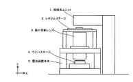
以下、本発明の実施例1について説明する。図1は本発明の実施例1にかかる露光装置の概略図である。照明系ユニット1は、光源と、光源からの光を成形して均一な露光光とする光学素子を有する。照明系ユニット1から照射された露光光は、レチクルステージ2上のレチクル(原版)を透過し、レチクルのパターンは縮小投影レンズ3を介してウエハステージ4上のウエハに縮小投影される。レチクルステージ2、投影レンズ3、およびウエハステージ4は露光装置本体5によって支持される。なお、露光装置の全体構成については例示的に示したものであり、他の構成であってもよい。
図2(1)はレチクルステージ2を露光光軸方向(Z方向)から見た図であり、図2(2)はスキャン方向(Y方向)から見た断面図である。スリット露光光8は、図のように、スリット状に成形され、レチクルステージ2とウエハステージ4を同期してスキャン駆動して露光を行う。レチクルステージ2はリニアモータによって駆動され、リニアモータは固定子10と可動子11を有する。レチクル6は、レチクルステージ2上にレチクルクランプ7を介して保持されている。
2A is a view of the
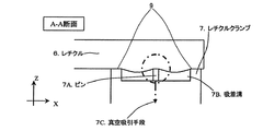
図3を用いてレチクルクランプ7によるレチクル6の保持方法について説明する。図3(1)は、レチクルクランプ7の上面に、レチクル6が保持されている状態を示す平面図であり、図3(2)は、図3(1)におけるクランプ状態を示すスキャン方向断面図(A−A断面図)であり、図3(3)はクランプ状態を示す非スキャン方向断面図(B−B断面図)である。 A method of holding the reticle 6 by the reticle clamp 7 will be described with reference to FIG. FIG. 3A is a plan view showing a state in which the reticle 6 is held on the upper surface of the reticle clamp 7, and FIG. 3B is a cross-sectional view in the scanning direction showing the clamped state in FIG. FIG. 3 (3) is a non-scan direction sectional view (BB sectional view) showing a clamped state.
ここで、レチクルクランプ7は、保持面9と、複数のピン7Aと、複数のピンの周囲に設けられた吸着溝7Bと、吸着溝7Bが形成する空間(気体)を真空吸引する真空吸引手段7Cを備える。真空吸引手段7Cは、例えば配管と配管に接続された真空ポンプ(不図示)により構成される。ピン7Aは先端面でレチクル6を支持可能である。溝7Bが形成する空間を真空吸引することによって、レチクル6はXYZ方向で位置決めした状態でピンの先端面(上面)および保持面に吸着保持される。
Here, the reticle clamp 7 includes a holding surface 9, a plurality of
図4はレチクルの吸着時と非吸着時の様子を表す図である。図4は図3(1)のB−B断面図である。 FIG. 4 is a diagram illustrating a state when the reticle is attracted and not attracted. 4 is a cross-sectional view taken along the line BB in FIG.
図4(a)はレチクルの非吸着時を表す図である。このとき、レチクル6は、レチクルクランプ7に対して、XYZ方向で位置決めされた後に搭載される。初期状態であるレチクル6の非吸着時には、レチクル6は自重によるたわみを生じるため、レチクル6は露光領域(露光光軸)側がレチクルクランプ7に接触し、端部は非接触となる。 FIG. 4A is a diagram illustrating the time when the reticle is not attracted. At this time, the reticle 6 is mounted after being positioned in the XYZ directions with respect to the reticle clamp 7. At the time of non-adsorption of the reticle 6 in the initial state, the reticle 6 is deflected by its own weight, so that the reticle 6 comes into contact with the reticle clamp 7 on the exposure area (exposure optical axis) side, and the end is not in contact.
真空吸引手段7Cにより真空吸引されると(図4(b))、レチクル6はピン7Aに接触するようになるため、レチクル6がレチクルクランプ7と接触する支点7Dが増加する。
When vacuum suction is performed by the vacuum suction means 7C (FIG. 4B), the reticle 6 comes into contact with the
支点7Dが増加すると、テコの原理の支点と、吸着力の作用点との距離が短くなるため、レチクル6を吸着保持した際の歪の発生を抑えることができる。 When the fulcrum 7D is increased, the distance between the fulcrum of the lever principle and the point of action of the suction force is shortened, so that the occurrence of distortion when holding the reticle 6 by suction can be suppressed.
また、図5および図6に示すように、レチクル6を吸着保持すると、レチクル6はピン7Aにめり込むような変形をする。このような変形が形成する凹凸形状がレチクル6側にピン7Aとの接触面に数箇所発生し、スパイク効果が生じる。
As shown in FIGS. 5 and 6, when the reticle 6 is sucked and held, the reticle 6 is deformed so as to sink into the
一般的に、摩擦力の微視的機構として凹凸説と凝着説が知られており、前者は接触面で凹凸が多いほど摩擦は大きくなるとする説であり、後者は接触面での原子と原子の結合が強いと摩擦は大きくなるとする説である。上述のスパイク効果は凹凸説を利用したものであり、吸着保持時に凹凸形状が増えることにより、摩擦力が大きくなり、数μm〜数nmのレチクル位置ずれを低減する効果を奏する。このようなスパイク効果はXY方向で位置ずれを低減する。 In general, the unevenness theory and the adhesion theory are known as microscopic mechanisms of frictional force. The former is a theory that friction increases as the unevenness increases on the contact surface. It is the theory that the friction increases when the bond of atoms is strong. The spike effect described above utilizes the unevenness theory, and increases the unevenness shape when holding the suction, thereby increasing the frictional force and reducing the reticle positional deviation of several μm to several nm. Such a spike effect reduces misalignment in the XY directions.
なお、本実施例において真空吸着によってレチクルを保持したが、静電吸着によってレチクルを保持するようにしても同様の効果を奏する。 In this embodiment, the reticle is held by vacuum suction. However, the same effect can be obtained even if the reticle is held by electrostatic suction.
次に、本発明の実施例2として、上記実施例1の露光装置を利用した半導体デバイスの製造プロセスを説明する。図7は半導体デバイスの全体的な製造プロセスのフローを示す図である。ステップ1(回路設計)では半導体デバイスの回路設計を行う。ステップ2(マスク製作)では設計した回路パターンに基づいてマスクを作製する。 Next, as a second embodiment of the present invention, a semiconductor device manufacturing process using the exposure apparatus of the first embodiment will be described. FIG. 7 is a diagram showing a flow of an entire manufacturing process of a semiconductor device. In step 1 (circuit design), a semiconductor device circuit is designed. In step 2 (mask production), a mask is produced based on the designed circuit pattern.
一方、ステップ3(ウエハ製造)ではシリコン等の材料を用いてウエハを製造する。ステップ4(ウエハプロセス)は前工程と呼ばれ、上記のマスクとウエハを用いて、上記の露光装置によりリソグラフィ技術を利用してウエハ上に実際の回路を形成する。次のステップ5(組み立て)は後工程と呼ばれ、ステップ4によって作製されたウエハを用いて半導体チップ化する工程であり、アッセンブリ工程(ダイシング、ボンディング)、パッケージング工程(チップ封入)等の組み立て工程を含む。ステップ6(検査)ではステップ5で作製された半導体デバイスの動作確認テスト、耐久性テスト等の検査を行う。こうした工程を経て半導体デバイスが完成し、ステップ7でこれを出荷する。 On the other hand, in step 3 (wafer manufacture), a wafer is manufactured using a material such as silicon. Step 4 (wafer process) is called a pre-process, and an actual circuit is formed on the wafer by using the above-described exposure apparatus and lithography technology using the above-described mask and wafer. The next step 5 (assembly) is called a post-process, and is a process for forming a semiconductor chip using the wafer produced in step 4, and is an assembly process (dicing, bonding), packaging process (chip encapsulation), etc. Process. In step 6 (inspection), the semiconductor device manufactured in step 5 undergoes inspections such as an operation confirmation test and a durability test. A semiconductor device is completed through these processes, and is shipped in Step 7.
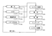
上記ステップ4のウエハプロセスは以下のステップを有する(図8)。ウエハの表面を酸化させる酸化ステップ(ステップ11)、ウエハ表面に絶縁膜を成膜するCVDステップ(ステップ12)、ウエハ上に電極を蒸着によって形成する電極形成ステップ(ステップ13)、ウエハにイオンを打ち込むイオン打ち込みステップ(ステップ14)、ウエハに感光剤を塗布するレジスト処理ステップ(ステップ15)、上記の露光装置によって回路パターンをレジスト処理ステップ後のウエハに転写する露光ステップ(ステップ16)、露光ステップで露光したウエハを現像する現像ステップ(ステップ17)、現像ステップで現像したレジスト像以外の部分を削り取るエッチングステップ(ステップ18)、エッチングが済んで不要となったレジストを取り除くレジスト剥離ステップ(ステップ19)。これらのステップを繰り返し行うことによって、ウエハ上に多重に回路パターンを形成する。 The wafer process in Step 4 has the following steps (FIG. 8). An oxidation step for oxidizing the surface of the wafer (step 11), a CVD step for forming an insulating film on the wafer surface (step 12), an electrode forming step for forming electrodes on the wafer by vapor deposition (step 13), and ions on the wafer Ion implantation step for implanting (step 14), resist processing step for applying a photosensitive agent to the wafer (step 15), exposure step for transferring a circuit pattern to the wafer after the resist processing step by the exposure apparatus (step 16), exposure step A developing step (step 17) for developing the wafer exposed in step (1), an etching step (step 18) for removing portions other than the resist image developed in the developing step, and a resist stripping step (step 19) for removing the resist that has become unnecessary after the etching. ). By repeating these steps, multiple circuit patterns are formed on the wafer.
このように実施例1における露光装置を用いてデバイスを製造することによって微細な回路パターンを形成することができる。 Thus, a fine circuit pattern can be formed by manufacturing a device using the exposure apparatus according to the first embodiment.
1:照明系ユニット、2:レチクルステージ、3:縮小投影レンズ、4:ウエハステージ、4A:ウエハ、5:露光装置本体、6:レチクル、7:レチクルクランプ、7A:ピン、7B:吸着溝、7C:真空吸引手段、7D:支点、7E:スパイク効果、8:スリット露光光、9:保持面、10:リニアモータ固定子、11:リニアモータ可動子。
(従来例) 101:レチクル、102:レチクルステージ、103:レチクルクランプ、103A:レチクルクランプパッド、103B:加速時の力、103C:加速時にかかる慣性力(G)、103D:支点、104:縮小投影レンズ、105:ウエハ、106:ウエハステージ。
1: illumination system unit, 2: reticle stage, 3: reduction projection lens, 4: wafer stage, 4A: wafer, 5: exposure apparatus body, 6: reticle, 7: reticle clamp, 7A: pin, 7B: suction groove, 7C: vacuum suction means, 7D: fulcrum, 7E: spike effect, 8: slit exposure light, 9: holding surface, 10: linear motor stator, 11: linear motor movable element.
(Conventional example) 101: reticle, 102: reticle stage, 103: reticle clamp, 103A: reticle clamp pad, 103B: force during acceleration, 103C: inertial force (G) applied during acceleration, 103D: fulcrum, 104: reduced projection Lens, 105: wafer, 106: wafer stage.
Claims (6)
前記原版を保持するための保持面を備える保持部を複数有し、
該保持部は前記原版を支持する複数の凸状支持部を備えることを特徴とする原版保持装置。 An original holding apparatus for holding an original having a pattern to be transferred to a substrate in an exposure apparatus,
Having a plurality of holding portions each having a holding surface for holding the original plate;
The original holding apparatus, wherein the holding part includes a plurality of convex support parts for supporting the original.
Priority Applications (2)
| Application Number | Priority Date | Filing Date | Title |
|---|---|---|---|
| JP2005072291A JP2006261156A (en) | 2005-03-15 | 2005-03-15 | Apparatus for holding original plate and exposure apparatus using the same |
| US11/371,100 US20060209289A1 (en) | 2005-03-15 | 2006-03-09 | Exposure apparatus, and device manufacturing method |
Applications Claiming Priority (1)
| Application Number | Priority Date | Filing Date | Title |
|---|---|---|---|
| JP2005072291A JP2006261156A (en) | 2005-03-15 | 2005-03-15 | Apparatus for holding original plate and exposure apparatus using the same |
Publications (2)
| Publication Number | Publication Date |
|---|---|
| JP2006261156A true JP2006261156A (en) | 2006-09-28 |
| JP2006261156A5 JP2006261156A5 (en) | 2008-05-01 |
Family
ID=37009943
Family Applications (1)
| Application Number | Title | Priority Date | Filing Date |
|---|---|---|---|
| JP2005072291A Withdrawn JP2006261156A (en) | 2005-03-15 | 2005-03-15 | Apparatus for holding original plate and exposure apparatus using the same |
Country Status (2)
| Country | Link |
|---|---|
| US (1) | US20060209289A1 (en) |
| JP (1) | JP2006261156A (en) |
Cited By (1)
| Publication number | Priority date | Publication date | Assignee | Title |
|---|---|---|---|---|
| KR101013943B1 (en) * | 2007-04-19 | 2011-02-14 | 캐논 가부시끼가이샤 | Stage apparatus, exposure apparatus, and device manufacturing method |
Families Citing this family (1)
| Publication number | Priority date | Publication date | Assignee | Title |
|---|---|---|---|---|
| US20130250271A1 (en) * | 2012-02-17 | 2013-09-26 | Nikon Corporation | Stage assembly with secure device holder |
Family Cites Families (7)
| Publication number | Priority date | Publication date | Assignee | Title |
|---|---|---|---|---|
| EP1077393A2 (en) * | 1999-08-19 | 2001-02-21 | Canon Kabushiki Kaisha | Substrate attracting and holding system for use in exposure apparatus |
| CN1507649A (en) * | 2001-02-13 | 2004-06-23 | 株式会社尼康 | Holding device, holding method, exposure device, and device manufacturing method |
| JP2002305138A (en) * | 2001-04-05 | 2002-10-18 | Nikon Corp | Aligner and method for exposure |
| EP1510868A1 (en) * | 2003-08-29 | 2005-03-02 | ASML Netherlands B.V. | Lithographic apparatus and device manufacturing method |
| EP1530089B1 (en) * | 2003-11-05 | 2011-04-06 | ASML Netherlands B.V. | Lithographic apparatus and method for clamping an article |
| JP4411100B2 (en) * | 2004-02-18 | 2010-02-10 | キヤノン株式会社 | Exposure equipment |
| JP4794882B2 (en) * | 2005-03-25 | 2011-10-19 | キヤノン株式会社 | Scanning exposure apparatus and scanning exposure method |
-
2005
- 2005-03-15 JP JP2005072291A patent/JP2006261156A/en not_active Withdrawn
-
2006
- 2006-03-09 US US11/371,100 patent/US20060209289A1/en not_active Abandoned
Cited By (1)
| Publication number | Priority date | Publication date | Assignee | Title |
|---|---|---|---|---|
| KR101013943B1 (en) * | 2007-04-19 | 2011-02-14 | 캐논 가부시끼가이샤 | Stage apparatus, exposure apparatus, and device manufacturing method |
Also Published As
| Publication number | Publication date |
|---|---|
| US20060209289A1 (en) | 2006-09-21 |
Similar Documents
| Publication | Publication Date | Title |
|---|---|---|
| US7307698B2 (en) | Exposure apparatus and device manufacturing method | |
| KR102134207B1 (en) | Holder, lithography apparatus, method of manufacturing article, and stage apparatus | |
| JP2008103703A (en) | Substrate retaining unit, exposure apparatus provided with substrate retaining unit, and device manufacturing method | |
| JP5656392B2 (en) | Substrate holding apparatus, exposure apparatus using the same, and device manufacturing method | |
| KR20080026499A (en) | Substrate-retaining unit | |
| KR100882046B1 (en) | Exposure apparatus and device manufacturing method | |
| US20090044837A1 (en) | Substrate processing apparatus | |
| JP2020112695A (en) | Exposure apparatus, exposure method and method for manufacturing article | |
| JP4447872B2 (en) | Stage apparatus, exposure apparatus using the stage apparatus, and device manufacturing method using the exposure apparatus | |
| JP4411158B2 (en) | Exposure equipment | |
| JP2001118776A (en) | Transfer aligner, and mask holding mechanism used for that device, and manufacturing method of semiconductor element | |
| JP2001144168A (en) | Electrostatic chuck, charged particle beam exposure system having the same, and wafer holding method and device manufacturing method using the chuck | |
| JP2010182866A (en) | Electrostatic attraction holding device, aligner, exposure method, and method of manufacturing device | |
| JP2002305138A (en) | Aligner and method for exposure | |
| JP2006261156A (en) | Apparatus for holding original plate and exposure apparatus using the same | |
| JP4309992B2 (en) | Sample holding device and exposure apparatus using the holding device | |
| JP2005228978A (en) | Exposure device and manufacturing method for semiconductor device | |
| JP2005044893A (en) | Substrate holding apparatus | |
| CN114999987A (en) | Chuck, substrate holding device, substrate processing device, and method for manufacturing article | |
| JP2022134074A (en) | Chuck, substrate-holding device, substrate-processing device, and production method of article | |
| JP4636807B2 (en) | Substrate holding device and exposure apparatus using the same | |
| JP2005116849A (en) | Electrostatic adsorption device and method therefor, exposure device, and device manufacturing method | |
| JP2004165439A (en) | Stage equipment | |
| JP2007207996A (en) | Substrate holding device | |
| JP2009177126A (en) | Mask blanks, mask, mask holding apparatus, exposure apparatus and method for manufacturing device |
Legal Events
| Date | Code | Title | Description |
|---|---|---|---|
| A521 | Written amendment |
Free format text: JAPANESE INTERMEDIATE CODE: A523 Effective date: 20080314 |
|
| A621 | Written request for application examination |
Free format text: JAPANESE INTERMEDIATE CODE: A621 Effective date: 20080314 |
|
| RD02 | Notification of acceptance of power of attorney |
Free format text: JAPANESE INTERMEDIATE CODE: A7422 Effective date: 20080314 |
|
| A072 | Dismissal of procedure [no reply to invitation to correct request for examination] |
Free format text: JAPANESE INTERMEDIATE CODE: A072 Effective date: 20080702 |
|
| RD01 | Notification of change of attorney |
Free format text: JAPANESE INTERMEDIATE CODE: A7421 Effective date: 20090406 |
|
| A761 | Written withdrawal of application |
Free format text: JAPANESE INTERMEDIATE CODE: A761 Effective date: 20100129 |
|
| RD04 | Notification of resignation of power of attorney |
Free format text: JAPANESE INTERMEDIATE CODE: A7424 Effective date: 20100201 |