JP2006196668A - Semiconductor device and manufacturing method of the same - Google Patents
Semiconductor device and manufacturing method of the same Download PDFInfo
- Publication number
- JP2006196668A JP2006196668A JP2005006433A JP2005006433A JP2006196668A JP 2006196668 A JP2006196668 A JP 2006196668A JP 2005006433 A JP2005006433 A JP 2005006433A JP 2005006433 A JP2005006433 A JP 2005006433A JP 2006196668 A JP2006196668 A JP 2006196668A
- Authority
- JP
- Japan
- Prior art keywords
- wiring
- insulating film
- semiconductor substrate
- film
- interlayer insulating
- Prior art date
- Legal status (The legal status is an assumption and is not a legal conclusion. Google has not performed a legal analysis and makes no representation as to the accuracy of the status listed.)
- Pending
Links
Images


Classifications
-
- H—ELECTRICITY
- H01—ELECTRIC ELEMENTS
- H01L—SEMICONDUCTOR DEVICES NOT COVERED BY CLASS H10
- H01L23/00—Details of semiconductor or other solid state devices
- H01L23/52—Arrangements for conducting electric current within the device in operation from one component to another, i.e. interconnections, e.g. wires, lead frames
- H01L23/522—Arrangements for conducting electric current within the device in operation from one component to another, i.e. interconnections, e.g. wires, lead frames including external interconnections consisting of a multilayer structure of conductive and insulating layers inseparably formed on the semiconductor body
- H01L23/532—Arrangements for conducting electric current within the device in operation from one component to another, i.e. interconnections, e.g. wires, lead frames including external interconnections consisting of a multilayer structure of conductive and insulating layers inseparably formed on the semiconductor body characterised by the materials
- H01L23/5329—Insulating materials
- H01L23/53295—Stacked insulating layers
-
- H—ELECTRICITY
- H01—ELECTRIC ELEMENTS
- H01L—SEMICONDUCTOR DEVICES NOT COVERED BY CLASS H10
- H01L21/00—Processes or apparatus adapted for the manufacture or treatment of semiconductor or solid state devices or of parts thereof
- H01L21/67—Apparatus specially adapted for handling semiconductor or electric solid state devices during manufacture or treatment thereof; Apparatus specially adapted for handling wafers during manufacture or treatment of semiconductor or electric solid state devices or components ; Apparatus not specifically provided for elsewhere
- H01L21/683—Apparatus specially adapted for handling semiconductor or electric solid state devices during manufacture or treatment thereof; Apparatus specially adapted for handling wafers during manufacture or treatment of semiconductor or electric solid state devices or components ; Apparatus not specifically provided for elsewhere for supporting or gripping
- H01L21/6835—Apparatus specially adapted for handling semiconductor or electric solid state devices during manufacture or treatment thereof; Apparatus specially adapted for handling wafers during manufacture or treatment of semiconductor or electric solid state devices or components ; Apparatus not specifically provided for elsewhere for supporting or gripping using temporarily an auxiliary support
-
- H—ELECTRICITY
- H01—ELECTRIC ELEMENTS
- H01L—SEMICONDUCTOR DEVICES NOT COVERED BY CLASS H10
- H01L21/00—Processes or apparatus adapted for the manufacture or treatment of semiconductor or solid state devices or of parts thereof
- H01L21/70—Manufacture or treatment of devices consisting of a plurality of solid state components formed in or on a common substrate or of parts thereof; Manufacture of integrated circuit devices or of parts thereof
- H01L21/71—Manufacture of specific parts of devices defined in group H01L21/70
- H01L21/768—Applying interconnections to be used for carrying current between separate components within a device comprising conductors and dielectrics
-
- H—ELECTRICITY
- H01—ELECTRIC ELEMENTS
- H01L—SEMICONDUCTOR DEVICES NOT COVERED BY CLASS H10
- H01L23/00—Details of semiconductor or other solid state devices
- H01L23/52—Arrangements for conducting electric current within the device in operation from one component to another, i.e. interconnections, e.g. wires, lead frames
- H01L23/522—Arrangements for conducting electric current within the device in operation from one component to another, i.e. interconnections, e.g. wires, lead frames including external interconnections consisting of a multilayer structure of conductive and insulating layers inseparably formed on the semiconductor body
- H01L23/5222—Capacitive arrangements or effects of, or between wiring layers
-
- H—ELECTRICITY
- H01—ELECTRIC ELEMENTS
- H01L—SEMICONDUCTOR DEVICES NOT COVERED BY CLASS H10
- H01L23/00—Details of semiconductor or other solid state devices
- H01L23/52—Arrangements for conducting electric current within the device in operation from one component to another, i.e. interconnections, e.g. wires, lead frames
- H01L23/522—Arrangements for conducting electric current within the device in operation from one component to another, i.e. interconnections, e.g. wires, lead frames including external interconnections consisting of a multilayer structure of conductive and insulating layers inseparably formed on the semiconductor body
- H01L23/528—Geometry or layout of the interconnection structure
- H01L23/5283—Cross-sectional geometry
-
- H—ELECTRICITY
- H01—ELECTRIC ELEMENTS
- H01L—SEMICONDUCTOR DEVICES NOT COVERED BY CLASS H10
- H01L2221/00—Processes or apparatus adapted for the manufacture or treatment of semiconductor or solid state devices or of parts thereof covered by H01L21/00
- H01L2221/67—Apparatus for handling semiconductor or electric solid state devices during manufacture or treatment thereof; Apparatus for handling wafers during manufacture or treatment of semiconductor or electric solid state devices or components; Apparatus not specifically provided for elsewhere
- H01L2221/683—Apparatus for handling semiconductor or electric solid state devices during manufacture or treatment thereof; Apparatus for handling wafers during manufacture or treatment of semiconductor or electric solid state devices or components; Apparatus not specifically provided for elsewhere for supporting or gripping
- H01L2221/68304—Apparatus for handling semiconductor or electric solid state devices during manufacture or treatment thereof; Apparatus for handling wafers during manufacture or treatment of semiconductor or electric solid state devices or components; Apparatus not specifically provided for elsewhere for supporting or gripping using temporarily an auxiliary support
- H01L2221/68363—Apparatus for handling semiconductor or electric solid state devices during manufacture or treatment thereof; Apparatus for handling wafers during manufacture or treatment of semiconductor or electric solid state devices or components; Apparatus not specifically provided for elsewhere for supporting or gripping using temporarily an auxiliary support used in a transfer process involving transfer directly from an origin substrate to a target substrate without use of an intermediate handle substrate
-
- H—ELECTRICITY
- H01—ELECTRIC ELEMENTS
- H01L—SEMICONDUCTOR DEVICES NOT COVERED BY CLASS H10
- H01L23/00—Details of semiconductor or other solid state devices
- H01L23/52—Arrangements for conducting electric current within the device in operation from one component to another, i.e. interconnections, e.g. wires, lead frames
- H01L23/522—Arrangements for conducting electric current within the device in operation from one component to another, i.e. interconnections, e.g. wires, lead frames including external interconnections consisting of a multilayer structure of conductive and insulating layers inseparably formed on the semiconductor body
- H01L23/532—Arrangements for conducting electric current within the device in operation from one component to another, i.e. interconnections, e.g. wires, lead frames including external interconnections consisting of a multilayer structure of conductive and insulating layers inseparably formed on the semiconductor body characterised by the materials
- H01L23/53204—Conductive materials
- H01L23/53209—Conductive materials based on metals, e.g. alloys, metal silicides
- H01L23/53228—Conductive materials based on metals, e.g. alloys, metal silicides the principal metal being copper
- H01L23/53238—Additional layers associated with copper layers, e.g. adhesion, barrier, cladding layers
-
- H—ELECTRICITY
- H01—ELECTRIC ELEMENTS
- H01L—SEMICONDUCTOR DEVICES NOT COVERED BY CLASS H10
- H01L2924/00—Indexing scheme for arrangements or methods for connecting or disconnecting semiconductor or solid-state bodies as covered by H01L24/00
- H01L2924/0001—Technical content checked by a classifier
- H01L2924/0002—Not covered by any one of groups H01L24/00, H01L24/00 and H01L2224/00
-
- H—ELECTRICITY
- H01—ELECTRIC ELEMENTS
- H01L—SEMICONDUCTOR DEVICES NOT COVERED BY CLASS H10
- H01L2924/00—Indexing scheme for arrangements or methods for connecting or disconnecting semiconductor or solid-state bodies as covered by H01L24/00
- H01L2924/19—Details of hybrid assemblies other than the semiconductor or other solid state devices to be connected
- H01L2924/1901—Structure
- H01L2924/1904—Component type
- H01L2924/19041—Component type being a capacitor
-
- H—ELECTRICITY
- H01—ELECTRIC ELEMENTS
- H01L—SEMICONDUCTOR DEVICES NOT COVERED BY CLASS H10
- H01L2924/00—Indexing scheme for arrangements or methods for connecting or disconnecting semiconductor or solid-state bodies as covered by H01L24/00
- H01L2924/30—Technical effects
- H01L2924/301—Electrical effects
- H01L2924/30105—Capacitance
Landscapes
- Engineering & Computer Science (AREA)
- Physics & Mathematics (AREA)
- Condensed Matter Physics & Semiconductors (AREA)
- General Physics & Mathematics (AREA)
- Computer Hardware Design (AREA)
- Microelectronics & Electronic Packaging (AREA)
- Power Engineering (AREA)
- Manufacturing & Machinery (AREA)
- Geometry (AREA)
- Internal Circuitry In Semiconductor Integrated Circuit Devices (AREA)
Abstract
Description
本発明は、例えばlow−k(low-dielectric constant:低誘電率)絶縁膜を用いた多層配線に係り、特に、2層以上の配線層を積層した半導体装置およびその製造方法に関する。 The present invention relates to a multilayer wiring using, for example, a low-k (low-dielectric constant) insulating film, and more particularly to a semiconductor device in which two or more wiring layers are stacked and a manufacturing method thereof.
近年、コンピューターや通信機器には、多数のトランジスタや抵抗などからなる電気回路を1チップ上に集積化した大規模集積回路(LSI)が多用されている。このため、機器全体の性能は、LSI単体に依存している。LSI単体の性能向上は、集積度を高めること、つまり、素子の微細化により実現できる。 2. Description of the Related Art In recent years, large scale integrated circuits (LSIs) in which electrical circuits composed of a large number of transistors, resistors, and the like are integrated on one chip are frequently used in computers and communication devices. For this reason, the performance of the entire device depends on the LSI alone. The improvement of the performance of a single LSI can be realized by increasing the degree of integration, that is, by miniaturizing elements.
しかしながら、素子の微細化により、配線間の容量結合に起因する信号の遅延が増大し、素子の高速動作を阻害する問題が顕著になってきている。そこで、配線間容量を低減させるため、比誘電率の小さな絶縁膜材料が使用されてきている。また、絶縁膜材料以外による配線間容量の低減方法としては、対向する配線の膜厚を薄くして対向面積を小さくする方法がある。配線間容量の低減としてすすめられてきている低誘電率材料の導入と、配線の薄膜化には次のような問題がある。 However, with the miniaturization of elements, signal delay due to capacitive coupling between wirings increases, and the problem of hindering high-speed operation of the elements has become prominent. Therefore, in order to reduce the capacitance between wirings, insulating film materials having a small relative dielectric constant have been used. Further, as a method of reducing the capacitance between wirings other than the insulating film material, there is a method of reducing the opposing area by reducing the thickness of the opposing wiring. The introduction of a low dielectric constant material, which has been promoted to reduce the capacitance between wires, and the thinning of wires have the following problems.
即ち、近年の絶縁膜の低誘電率化は絶縁膜の材料を変更するのみではその要求に十分応じることができない。このため、絶縁膜自体の比誘電率を下げ、さらに絶縁膜の密度を下げることで達成されようとしている。この場合、低誘電率化された絶縁膜の機械的強度や密着性が減少するため、機械的ストレスや、成膜プロセスや熱処理などの熱ストレスに対する耐性が著しく低下する。特に、多層に積層した配線を形成する場合、幾度もの成膜プロセスや熱処理、CMP(化学的機械的研磨)処理が行なわれるため、絶縁膜の機械的ストレスや、熱ストレスに対する耐性が著しく低下する。 In other words, the recent reduction in dielectric constant of an insulating film cannot sufficiently meet the demand by simply changing the material of the insulating film. For this reason, it is going to be achieved by lowering the relative dielectric constant of the insulating film itself and further lowering the density of the insulating film. In this case, since the mechanical strength and adhesion of the insulating film having a low dielectric constant are reduced, resistance to mechanical stress and thermal stress such as a film forming process and heat treatment is significantly reduced. In particular, in the case of forming a multi-layered wiring, since the film forming process, heat treatment, and CMP (chemical mechanical polishing) are performed many times, the resistance of the insulating film to mechanical stress and thermal stress is significantly reduced. .
また、同様に配線を薄膜化した場合、微細配線が多層に積層された場合、成膜プロセスや熱処理などの熱ストレスのサイクルによってストレスマイグレーションなど、配線の信頼性低下を引き起こす懸念がある。 Similarly, when the wiring is thinned, when fine wiring is stacked in multiple layers, there is a concern that the reliability of the wiring may be reduced due to stress migration due to a thermal stress cycle such as a film forming process or heat treatment.
このように、高性能化、高集積化がすすむLSIの多層配線において、低誘電率絶縁膜や微細な配線の機械的/熱的ストレスをいかに抑えるかが重要になってくる。 As described above, in LSI multi-layer wiring that is required to have high performance and high integration, it is important to suppress mechanical / thermal stress of a low dielectric constant insulating film and fine wiring.
従来、多層配線構造の品質向上及び製造時間の短縮化を目的として、複数の多層配線領域をそれぞれ個別に形成する製造方法が提案されている(例えば特許文献1参照)。 Conventionally, a manufacturing method for individually forming a plurality of multilayer wiring regions has been proposed for the purpose of improving the quality of the multilayer wiring structure and shortening the manufacturing time (see, for example, Patent Document 1).
しかしながら、この製造方法では、low−k材料を用いた絶縁膜に対する機械的、熱的ストレスを十分に抑えることが困難であった。
本発明は、半導体素子に近い下層の配線や低誘電率絶縁膜に対する機械的/熱的ストレスを抑えた半導体装置及びその製造方法を提供する。 The present invention provides a semiconductor device that suppresses mechanical / thermal stress on a lower wiring or a low dielectric constant insulating film close to a semiconductor element, and a method for manufacturing the same.
本発明の半導体装置の態様は、半導体基板上に形成された半導体素子と、前記半導体基板上に積層された複数の絶縁膜と、前記複数の絶縁膜内にそれぞれ形成された複数の配線層と、前記各配線層の上面及び両側面を連続的に覆うバリアメタルとを具備することを特徴としている。 An aspect of a semiconductor device according to the present invention includes a semiconductor element formed on a semiconductor substrate, a plurality of insulating films stacked on the semiconductor substrate, and a plurality of wiring layers respectively formed in the plurality of insulating films. And a barrier metal that continuously covers the upper surface and both side surfaces of each wiring layer.
本発明の半導体装置の態様は、半導体基板内に形成された半導体素子と、前記半導体基板上に積層された複数の絶縁膜と、前記複数の絶縁膜内にそれぞれ形成された複数の配線層と、前記複数の絶縁膜内にそれぞれ形成され、複数の配線層を接続する複数のプラグと、前記複数の配線層のそれぞれとその上の前記プラグの上面及び両側面を連続的に覆うバリアメタルとを具備することを特徴としている。 An aspect of the semiconductor device of the present invention includes a semiconductor element formed in a semiconductor substrate, a plurality of insulating films stacked on the semiconductor substrate, and a plurality of wiring layers formed in the plurality of insulating films, respectively. A plurality of plugs respectively formed in the plurality of insulating films and connecting the plurality of wiring layers; a barrier metal continuously covering each of the plurality of wiring layers and the upper surface and both side surfaces of the plug thereon; It is characterized by comprising.
本発明の半導体装置の製造方法の態様は、第1の半導体基板上に上層配線層を形成し、前記上層配線層の上方に少なくとも下層配線層を形成し、前記第1の半導体基板上に形成された前記下層配線を、半導体素子を含む第2の半導体基板上に張り合わせることを特徴としている。 According to an aspect of the method for manufacturing a semiconductor device of the present invention, an upper wiring layer is formed on a first semiconductor substrate, at least a lower wiring layer is formed above the upper wiring layer, and formed on the first semiconductor substrate. The above-described lower layer wiring is pasted onto a second semiconductor substrate including a semiconductor element.
本発明の半導体装置の製造方法の態様は、第1の半導体基板上に第1の誘電率を有する第1の絶縁膜を形成し、前記第1の絶縁膜内に上層配線層を形成し、前記第1の絶縁膜の上方に前記第1の誘電率より低い第2の誘電率を有する第2の絶縁膜を形成し、前記第2の絶縁膜内に少なくとも下層配線層を形成し、前記第1の半導体基板上に形成された前記下層配線を、半導体素子を含む第2の半導体基板上に張り合わせることを特徴としている。 According to an aspect of the method for manufacturing a semiconductor device of the present invention, a first insulating film having a first dielectric constant is formed on a first semiconductor substrate, an upper wiring layer is formed in the first insulating film, Forming a second insulating film having a second dielectric constant lower than the first dielectric constant above the first insulating film; forming at least a lower wiring layer in the second insulating film; The lower layer wiring formed on the first semiconductor substrate is pasted onto the second semiconductor substrate including the semiconductor element.
本発明の半導体装置の製造方法の態様は、第1の半導体基板上に第1の誘電率を有する第1の絶縁膜を形成し、前記第1の絶縁膜内に上層配線層を形成し、第2の半導体基板上に前記第1の誘電率より低い第2の誘電率を有する第2の絶縁膜を形成し、前記第2の絶縁膜内に少なくとも下層配線層を形成し、前記第2の半導体基板上に形成された前記下層配線を、半導体素子を含む第3の半導体基板上に張り合わせ、前記第2の半導体基板を除去した後、前記第1の絶縁膜及び前記上層配線層を有する前記第1の半導体基板を前記第2の絶縁膜に張り合わせることを特徴としている。 According to an aspect of the method for manufacturing a semiconductor device of the present invention, a first insulating film having a first dielectric constant is formed on a first semiconductor substrate, an upper wiring layer is formed in the first insulating film, Forming a second insulating film having a second dielectric constant lower than the first dielectric constant on a second semiconductor substrate; forming at least a lower wiring layer in the second insulating film; and The lower wiring formed on the semiconductor substrate is bonded onto a third semiconductor substrate including a semiconductor element, and after removing the second semiconductor substrate, the first insulating film and the upper wiring layer are provided. The first semiconductor substrate is bonded to the second insulating film.
本発明によれば、半導体素子に近い下層の配線や低誘電率絶縁膜に対する機械的/熱的ストレスを抑えた半導体装置及びその製造方法を提供できる。 ADVANTAGE OF THE INVENTION According to this invention, the semiconductor device which suppressed the mechanical / thermal stress with respect to the lower layer wiring near a semiconductor element and a low dielectric constant insulating film, and its manufacturing method can be provided.
以下図面を参照して本発明の実施の形態を詳細に説明する。 Hereinafter, embodiments of the present invention will be described in detail with reference to the drawings.
(第1の実施形態)
図1は、第1の実施形態に係る半導体装置の構成を示している。この半導体装置は、例えば二つの半導体基板に形成された半導体装置と多層配線層を張り合わせて形成されている。すなわち、半導体基板11には、例えばMOSFET12と、MOSFET12を覆う絶縁膜13、この絶縁膜13内に形成され、MOSFET12の例えばソースに接続されたコンタクト14が形成されている。
(First embodiment)
FIG. 1 shows the configuration of the semiconductor device according to the first embodiment. This semiconductor device is formed, for example, by bonding a semiconductor device formed on two semiconductor substrates and a multilayer wiring layer. That is, on the
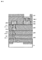
また、半導体基板(図示せず)には、第1の層間絶縁膜102、第2層間絶縁膜105、第3の層間絶縁膜107、第4の層間絶縁膜110、第5の層間絶縁膜112、第6の層間絶縁膜115、第7の層間絶縁膜117、第8の層間絶縁膜120、第9の層間絶縁膜122、拡散防止膜109、114、119、ボンディング電極104、最上層配線108、上層配線113、中間層配線118、下層配線123、接続プラグ106、ビアプラグ111、116、121が形成されている。第1、第2、第3、第4の層間絶縁膜102、105、107、110は、例えばシリコン酸化膜(SiO2)により形成され、第5、第6、第7、第8、第9の層間絶縁膜112、115、117、120、122は、low−k膜例えばSiOC(炭素含有シリコン酸化膜)により形成されている。これら層間絶縁膜、配線、ビアプラグは、図示せぬ半導体基板に対して、第1の層間絶縁膜102から第9の層間絶縁膜122と下層配線123へと順次形成される。すなわち、図示せぬ半導体基板に対して、上層配線から下層配線へと、通常の製造順序とは逆の順序により形成される。
In addition, the semiconductor substrate (not shown) includes a first interlayer
このように形成された第1の基板の絶縁膜13及びコンタクト14の表面に、第2の基板の第9の層間絶縁膜122と下層配線123が張り合わされ、図1に示す構成とされている。
The ninth
上記のように、上層の絶縁膜、配線及びビアプラグを下層の絶縁膜、配線及びビアプラグより先に形成することにより、low−k膜により構成された下層の絶縁膜、及び上層の配線に比べて膜厚が薄く、幅が狭い下層配線に対する機械的、熱的ストレスを緩和することができる。 As described above, by forming the upper insulating film, the wiring and the via plug before the lower insulating film, the wiring and the via plug, compared to the lower insulating film and the upper wiring composed of the low-k film. Mechanical and thermal stress on the lower layer wiring having a small thickness and a narrow width can be alleviated.
次に、図2乃至図7を参照して、第1の実施形態に係る半導体装置の製造方法について説明する。図2乃至図7は、図1に示す第2の基板上に多層配線を形成する場合を示しており、Cu配線及びプラグをシングルダマシーン(single-Damascene)プロセスを用いて形成する場合を示している。 Next, with reference to FIGS. 2 to 7, a method for manufacturing the semiconductor device according to the first embodiment will be described. 2 to 7 show a case where a multilayer wiring is formed on the second substrate shown in FIG. 1, and shows a case where a Cu wiring and a plug are formed using a single-Damascene process. ing.
尚、図1に示す第1の基板内における半導体装置の製造方法は、従来の製造方法と同様であるため説明は省略する。 The manufacturing method of the semiconductor device in the first substrate shown in FIG. 1 is the same as the conventional manufacturing method, and the description thereof is omitted.
まず、図2に示すように、半導体基板101に対し絶縁分離層となる第1の層間絶縁膜102を堆積する。その後、ボンディング電極となる図示せぬ開口を設け、この開口に犠牲膜103を形成する。次いで、犠牲膜103上にボンディング電極金属となるAl膜104を形成し、電極の形に加工する。次いで、例えばSiO2からなる第2の層間絶縁膜105を堆積し、平坦化処理を行う。
First, as shown in FIG. 2, a first interlayer
次に、図3に示すように、第2の層間絶縁膜105内にボンディング電極金属104を露出する複数の開口105−1を形成する。この後、第2の層間絶縁膜105上及び開口105−1の底面及び側面に例えばタンタルからなるバリアメタル106−1を形成し、このバリアメタル106−1の上にCu膜106−2を形成する。バリアメタル106−1は、Cuの拡散を防止する。次いで、例えばCMP(Chemical Mechanical Polishing)により、第2の層間絶縁膜105上のCu膜106−2及びバリアメタル106−1を平坦化し、開口105−1内に接続プラグ106を形成する。この接続プラグ106は、開口105−1の底部と側面に形成されたバリアメタル106−1と、Cu膜106−2とにより構成されている。
Next, as shown in FIG. 3, a plurality of openings 105-1 exposing the
次いで、第2の層間絶縁膜105上の全面に、例えばSiO2からなる第3の層間絶縁膜107を堆積する。この第3の層間絶縁膜107内に、図示せぬレジストをマスクとして、RIE(Reactive Ion Etching)により最上層配線を形成するための配線溝107−1を形成する。その後、第3の層間絶縁膜107上及び配線溝107−1の底面及び側面に例えばタンタルからなるバリアメタル108−1を形成し、このバリアメタル108−1の上にCu膜108−2を形成する。この後、例えばCMPにより、第3の層間絶縁膜107上のCu膜108−2及びバリアメタル108−1を平坦化し、配線溝107−1内に最上層配線108を形成する。この最上層配線108は、配線溝107−1の底部と側面に形成されたバリアメタル108−1とCu膜108−2とにより構成されている。この最上層配線108は、例えば電源線、データバス線、クロック線のようなチップ全体に配置された機能回路ブロック間の電気信号受け渡しを担うグローバル配線である。
Next, a third interlayer
以下、同様にして、配線及びコンタクトが順次形成される。尚、以下の説明において、バリアメタルと配線、コンタクトの詳細な製造工程は省略する。 Thereafter, wiring and contacts are sequentially formed in the same manner. In the following description, detailed manufacturing processes of the barrier metal, the wiring, and the contact are omitted.
図4に示すように、最上層配線108及び第3の層間絶縁膜107の上全面に最上層配線108のCuの拡散を防止する例えばSiCからなる拡散防止膜109を堆積する。その後、例えばSiO2からなる第4の層間絶縁膜110を基板全面に堆積させる。第4の層間絶縁膜110と拡散防止膜109に開口を形成し、この開口内に最上層配線108と上層配線とを接続するビアプラグ111を形成する。このビアプラグ111は、バリアメタル111−1で底部及び側面が連続的に覆われたCu膜111−2により形成されている。
As shown in FIG. 4, a
次いで、ビアプラグ111及び第4の層間絶縁膜110の上全面に第5の層間絶縁膜112を堆積する。この第5の層間絶縁膜112は、例えば無空孔のSiOCからなるlow−k膜である。この後、レジストをマスクとして、RIEにより上層配線を形成するための配線溝を形成する。この配線溝内に上層配線113を形成する。この上層配線は、バリアメタル113−1で底部及び側面が連続的に覆われたCu膜113−2により形成されている。上層配線113は、例えば制御信号やクロック分配支線、電源支線などの役割を担うセミグローバル配線である。
Next, a fifth
次に、図5に示すように、上層配線113及び第5の層間絶縁膜112の上全面にCuの拡散を防止する例えばSiC膜からなる拡散防止膜114を堆積する。この拡散防止膜114の上に、例えば無空孔のSiOCからなるlow−k膜である第6の層間絶縁膜115を堆積する。次いで、第6の層間絶縁膜115と拡散防止膜114に開口をする。この開口内にビアプラグ116を形成する。このビアプラグ116は、バリアメタル116−1で底部及び側面が連続的に覆われたCu膜116−2により形成されている。
Next, as shown in FIG. 5, a
次いで、第6の層間絶縁膜115とビアプラグ116の上全面に、例えば空孔率の大きいSiOCからなるlow−k膜である第7の層間絶縁膜117を堆積する。この後、レジストをマスクとして、RIEにより第7の層間絶縁膜117内に配線溝を形成する。この配線溝内に中間層配線118を形成する。この中間層配線118は、バリアメタル118−1で下方及び側面が連続的に覆われたCu膜118−2により構成されている。中間層配線118は、例えば単位回路ブロック内や隣接回路ブロック間を接続するインターメディエイト配線である。
Next, a seventh
次に、図6に示すように、第7の層間絶縁膜117と中間層配線118の上にCuの拡散を防止する例えばSiC膜からなる拡散防止膜119を形成する。この拡散防止膜119の上に、例えば空孔率の大きいSiOCからなるlow−k膜である第8の層間絶縁膜120を堆積させる。第8の層間絶縁膜120と拡散防止膜119に開口を設け、この開口内にビアプラグ121を形成する。このビアプラグ121は、バリアメタル121−1で底部及び側面が連続的に覆われたCu膜121−2により形成されている。
Next, as shown in FIG. 6, a
次いで、第8の層間絶縁膜120とビアプラグ121の上全面に例えば空孔率の大きいSiOCからなるlow−k膜である第9の層間絶縁膜122を堆積する。この後、レジストをマスクとして、RIEにより第9の層間絶縁膜122内に配線溝を形成する。この配線溝内に下層配線123を形成する。この下層配線123は、バリアメタル123−1で底部及び側面が連続的に覆われたCu膜123−2により形成されている。下層配線123は、例えばトランジスタやメモリセル内を接続するローカル配線である。この後、前記第9の層間絶縁膜122及び下層配線123の表面は鏡面状に仕上げられる。
Next, a ninth
次いで、図1に示すように、図2乃至図6で作製した多層配線が形成された半導体基板101とトランジスタが形成された半導体基板11とが貼り合わされる。すなわち、半導体基板101の上方に形成された下層配線金属123と、これとは別途形成された半導体基板11のコンタクト電極14とを接触させ貼り合わせる。
Next, as illustrated in FIG. 1, the
その後、基板101、犠牲膜103を順次剥離することにより、図1に示すような、半導体素子からボンディング電極の開口した半導体装置が形成される。
Thereafter, the
上記第1の実施形態によれば、従来とは逆に、上層、中層、下層の絶縁膜、配線及びビアプラグの順に形成している。このため、従来の製造方法により形成した場合、先に形成したlow−k膜が後に形成される層間絶縁膜や配線の形成に係るCMPにおける機械的ストレスや、熱処理における熱ストレスを受けるが、上記第1の実施形態によれば、low−k膜により構成された第5乃至第9の層間絶縁膜や、上層の配線に比べて膜厚が薄く、幅が狭い中間層配線118、下層配線123は、シリコン酸化膜により形成された第1乃至第4の層間絶縁膜や、上層の配線より後に形成される。したがって、low−k膜により構成された第5乃至第9の層間絶縁膜や、幅が狭い中間層配線118、下層配線123に対する機械的、熱的ストレスを緩和することができる。
According to the first embodiment, contrary to the prior art, the upper layer, middle layer, lower layer insulating film, wiring, and via plug are formed in this order. For this reason, when formed by a conventional manufacturing method, the low-k film formed earlier is subjected to mechanical stress in CMP related to formation of an interlayer insulating film and wiring to be formed later, and thermal stress in heat treatment. According to the first embodiment, the
(第2の実施形態)
図7乃至図9は、第2の実施形態を示している。
(Second Embodiment)
7 to 9 show a second embodiment.
第1の実施形態は、シングルダマシーン法で作製した下層、中間層、上層、最上層を含む4層配線の例であるが、図7に示すように、例えば最上層配線を2層(108a及び108b)、上層配線を4層(113a、113b、113c及び113d)、中間層配線を4層(118a、118b、118c及び118d)、下層配線を1層123の計11層あるいは更に多層の半導体装置に上記製造方法を適用することも可能である。 The first embodiment is an example of a four-layer wiring including a lower layer, an intermediate layer, an upper layer, and an uppermost layer manufactured by a single damascene method. For example, as shown in FIG. 108b), 4 layers of upper layer wiring (113a, 113b, 113c and 113d), 4 layers of intermediate layer wiring (118a, 118b, 118c and 118d), and 11 layers of lower layer wiring, totaling 11 layers or more layers. It is also possible to apply the above manufacturing method to the apparatus.
このように多層の配線を含む半導体装置を形成する場合、例えばlow−k膜を含む配線層とSiO2膜を含む配線層とを別々の半導体基板に形成し、これらを張り合わせることも可能である。 When forming a semiconductor device including multilayer wiring in this way, for example, a wiring layer including a low-k film and a wiring layer including a SiO 2 film can be formed on separate semiconductor substrates and bonded together. is there.
一般にlow−k膜はSiO2膜に比べて歩留りが低い。このため、これらを一緒に形成した場合、例えばlow−k膜が剥がれて、それがウェハ表面に付着してスクラッチが生じたりする。即ちlow−k膜の歩留りが製品全体の歩留りに影響してしまう。 In general, the low-k film has a lower yield than the SiO 2 film. For this reason, when these are formed together, for example, a low-k film is peeled off, and it adheres to the wafer surface, resulting in a scratch. That is, the yield of the low-k film affects the yield of the entire product.
そこで、第2の実施形態では、図7に示す半導体装置のうちlow−k膜を含む例えば下層及び中間層と、SiO2膜を含む上層及び最上層とをそれぞれ別個に形成する。 Therefore, in the second embodiment, for example, the lower layer and the intermediate layer including the low-k film and the upper layer and the uppermost layer including the SiO 2 film are separately formed in the semiconductor device shown in FIG.
すなわち、図8に示すように、半導体基板101上に、第1の実施形態と同様に、図7に示す最上層の部分と、上層の部分を形成する。また、図9に示すように、半導体基板201上に、図7に示す中間層の部分と下層の部分を順次形成する。半導体基板201上にこのように形成された下層の部分を、図7に示すように、MOSFETが形成された半導体基板11に張り合わせる。この後、半導体基板201を除去し、中間層の部分に図8に示す半導体基板101に形成された上層の部分を張り合わせる。この後、半導体基板101を除去した後、犠牲膜を除去して、図7に示す半導体装置を形成する。
That is, as shown in FIG. 8, the uppermost layer portion and the upper layer portion shown in FIG. 7 are formed on the
上記第2の実施形態によれば、low−k膜を含む例えば下層と中間層と、SiO2膜を含む上層と最上層をそれぞれ別の半導体基板上に製造し、これらをMOSFETが形成された半導体基板11に順次張り合わせている。このため、例えばlow−k膜を含む層を形成した後、これをスクリーニングして、良品のみを選択し、これをMOSFETが形成された半導体基板11と、SiO2膜を含む層との間に張り合わせて最終的な製品を作製すれば、low−k膜の歩留りの影響を除去することができ、製品全体としての歩留りを向上することが出来る。
According to the second embodiment, for example, a lower layer and an intermediate layer including a low-k film, and an upper layer and an uppermost layer including a SiO 2 film are manufactured on different semiconductor substrates, respectively, and MOSFETs are formed thereon. The
(第3の実施形態)
上記第1、第2の実施形態は、配線及びプラグを別々に形成するシングルダマシーン法を用いた製造方法について説明した。しかし、これに限らず、デュアルダマシーン法を用いて形成することも可能である。
(Third embodiment)
In the first and second embodiments, the manufacturing method using the single damascene method in which the wiring and the plug are separately formed has been described. However, the present invention is not limited to this, and it is also possible to form using a dual damascene method.
図10は、第3の実施形態に係る半導体装置を示している。この半導体装置は、MOSTEFを含む半導体基板11にデュアルダマシーン法を用いて形成した多層配線層を張り合わせた状態を示している。図10に示す半導体装置は、図1と同様に4層の配線層を有している。
FIG. 10 shows a semiconductor device according to the third embodiment. This semiconductor device shows a state in which a multilayer wiring layer formed by using a dual damascene method is bonded to a
各絶縁膜202−205には、配線及びプラグのための溝が一体的に形成され、この溝内に例えばタンタル等のバリアメタル206−1,211−1,216−1,221−1で覆われた配線及びプラグ206,211,216,221が一体的に形成されている。この多層配線の製造過程は、図10に示す形状を上下を逆とした状態でなされる。 Each insulating film 202-205 is integrally formed with a groove for wiring and a plug, and is covered with barrier metal 206-1, 211-1, 216-1, 212-1 such as tantalum in the groove. Broken wires and plugs 206, 211, 216, and 221 are integrally formed. The manufacturing process of the multilayer wiring is performed with the shape shown in FIG. 10 turned upside down.
上記のようにして形成された配線層は、半導体素子としてのMOSFETが形成された半導体基板に貼り合わせた状態において、プラグの上方がバリアメタルで塞がれている。 In the wiring layer formed as described above, the upper portion of the plug is closed with a barrier metal in a state where the wiring layer is bonded to a semiconductor substrate on which a MOSFET as a semiconductor element is formed.
上記第3の実施形態によれば、デュアルダマシーン法を用いて最上層の配線及びビアプラグから形成し始めて下層の配線及びビアプラグを最後に形成し、この後、下層の配線を半導体素子としてのMOSFETが形成された半導体基板に張り合わせている。このため、シングルダマシーン法を用いて形成した第1、第2の実施形態と同様に、low−k膜により構成された層間絶縁膜や、幅が狭い中間層配線、下層配線に対する機械的、熱的ストレスを緩和することができる。 According to the third embodiment, the dual damascene method is used to start forming the uppermost layer wiring and via plug, and finally form the lower layer wiring and via plug, and then form the lower layer wiring as a semiconductor element MOSFET. Is attached to the semiconductor substrate formed. For this reason, as in the first and second embodiments formed by using the single damascene method, the interlayer insulating film constituted by the low-k film, the intermediate layer wiring having a narrow width, the mechanical for the lower layer wiring, Thermal stress can be relieved.
しかも、デュアルダマシーン法を用いて配線とビアプラグを同時に形成した場合、次のような効果を得ることができる。図11に示すように、デュアルダマシーン法を用いた従来の製造方法により図10と同様の半導体装置を形成した場合、例えばバリアメタル311−1は、配線311と、この配線311の下方に位置するビアプラグ312の底部及び側面に形成される。しかも、下層配線から上層配線に向かって配線の幅、膜厚が大きくされている。上層配線のように、幅が広く、膜厚が厚い配線は、配線材料としてのCu膜内に多くの空孔を有している。このため、例えば最終的な熱処理において、配線311より下方に位置するビアプラグ312より、Cu元素が配線311に移動し、ビアプラグ312内にボイドが発生するおそれを有している。その他の層のプラグも同様にボイドが生じるおそれを有している。
In addition, when the wiring and the via plug are formed simultaneously using the dual damascene method, the following effects can be obtained. As shown in FIG. 11, when a semiconductor device similar to that of FIG. 10 is formed by a conventional manufacturing method using the dual damascene method, for example, the barrier metal 311-1 is positioned below the
これに対して、第3の実施形態の場合、図10に示すように、最終的に形成される半導体装置において、バリアメタル211−1は配線212と配線212上のビアプラグ211を一体的に覆っている。このため、例えば最終的な熱処理において、ビアプラグ211とその上方に位置する配線206との間にはバリアメタル211−1があるため、ビアプラグ211から上方の配線206へCu元素が移動することがない。しかも、ビアプラグ211の下の配線212は上層の配線206より幅が狭く膜厚も薄いため、下層の配線212内の空孔は上層の配線206より少ない。このため、ビアプラグ211から下層の配線212に移動するCu元素はごく僅かである。したがって、ビアプラグ211内にボイドが発生することを防止できる。その他の層の配線とビアプラグとの構成も配線212とビアプラグ211と同様であるため、各層のビアプラグ内にボイドが発生することを防止できる。
On the other hand, in the case of the third embodiment, as shown in FIG. 10, in the finally formed semiconductor device, the barrier metal 211-1 integrally covers the
なお、上記各実施形態は、多層配線とビアプラグの形成について説明した。しかし、これに限らず、多層配線部分には配線のみではなく、キャパシタなどの機能素子を作製することも可能である。 In the above embodiments, the formation of multilayer wiring and via plugs has been described. However, the present invention is not limited to this, and it is possible to fabricate not only the wiring but also a functional element such as a capacitor in the multilayer wiring portion.
その他、本発明の主旨を逸脱しない範囲で、種々変形実施可能なことは勿論である。 Of course, various modifications can be made without departing from the spirit of the present invention.
101…基板、102…第1の層間絶縁膜、103…犠牲膜、104…ボンディング電極(Al)、105…第2層間絶縁膜、106…接続プラグ(Cu)、107…第3の層間絶縁膜、108…最上層配線(Cu)、109、114、119…拡散防止膜(SiC)、110…第4の層間絶縁膜、111、116、121…ビアプラグ(Cu)、112…第5の層間絶縁膜、113…上層配線(Cu)、115…第6の層間絶縁膜、117…第7の層間絶縁膜、118…中間層配線(Cu)、120…第8の層間絶縁膜、122…第9の層間絶縁膜、123…下層配線(Cu)、14…コンタクト電極、106−1、108−1、111−1、113−1、116−1、118−1、121−1、123−1、211−1、216−1、221−1、311−1、316−1、321−1…バリアメタル、211、216,221、311、316、321…配線及びビアプラグ(Cu)。
DESCRIPTION OF
Claims (5)
前記半導体基板上に積層された複数の絶縁膜と、
前記複数の絶縁膜内にそれぞれ形成された複数の配線層と、
前記各配線層の上面及び両側面を連続的に覆うバリアメタルと
を具備することを特徴とする半導体装置。 A semiconductor element formed on a semiconductor substrate;
A plurality of insulating films stacked on the semiconductor substrate;
A plurality of wiring layers respectively formed in the plurality of insulating films;
And a barrier metal that continuously covers the upper surface and both side surfaces of each wiring layer.
前記半導体基板上に積層された複数の絶縁膜と、
前記複数の絶縁膜内にそれぞれ形成された複数の配線層と、
前記複数の絶縁膜内にそれぞれ形成され、複数の配線層を接続する複数のプラグと、
前記複数の配線層のそれぞれとその上の前記プラグの上面及び両側面を連続的に覆うバリアメタルと
を具備することを特徴とする半導体装置。 A semiconductor element formed in a semiconductor substrate;
A plurality of insulating films stacked on the semiconductor substrate;
A plurality of wiring layers respectively formed in the plurality of insulating films;
A plurality of plugs respectively formed in the plurality of insulating films and connecting a plurality of wiring layers;
A semiconductor device comprising: each of the plurality of wiring layers; and a barrier metal that continuously covers an upper surface and both side surfaces of the plug on the wiring layer.
前記上層配線層の上方に少なくとも下層配線層を形成し、
前記第1の半導体基板上に形成された前記下層配線を、半導体素子を含む第2の半導体基板上に張り合わせることを特徴とする半導体装置の製造方法。 Forming an upper wiring layer on the first semiconductor substrate;
Forming at least a lower wiring layer above the upper wiring layer;
A method of manufacturing a semiconductor device, comprising: bonding the lower layer wiring formed on the first semiconductor substrate onto a second semiconductor substrate including a semiconductor element.
前記第1の絶縁膜内に上層配線層を形成し、
前記第1の絶縁膜の上方に前記第1の誘電率より低い第2の誘電率を有する第2の絶縁膜を形成し、
前記第2の絶縁膜内に少なくとも下層配線層を形成し、
前記第1の半導体基板上に形成された前記下層配線を、半導体素子を含む第2の半導体基板上に張り合わせることを特徴とする半導体装置の製造方法。 Forming a first insulating film having a first dielectric constant on a first semiconductor substrate;
Forming an upper wiring layer in the first insulating film;
Forming a second insulating film having a second dielectric constant lower than the first dielectric constant on the first insulating film;
Forming at least a lower wiring layer in the second insulating film;
A method for manufacturing a semiconductor device, comprising: bonding the lower layer wiring formed on the first semiconductor substrate onto a second semiconductor substrate including a semiconductor element.
前記第1の絶縁膜内に上層配線層を形成し、
第2の半導体基板上に前記第1の誘電率より低い第2の誘電率を有する第2の絶縁膜を形成し、
前記第2の絶縁膜内に少なくとも下層配線層を形成し、
前記第2の半導体基板上に形成された前記下層配線を、半導体素子を含む第3の半導体基板上に張り合わせ、
前記第2の半導体基板を除去した後、前記第1の絶縁膜及び前記上層配線層を有する前記第1の半導体基板を前記第2の絶縁膜に張り合わせる
ことを特徴とする半導体装置の製造方法。 Forming a first insulating film having a first dielectric constant on a first semiconductor substrate;
Forming an upper wiring layer in the first insulating film;
Forming a second insulating film having a second dielectric constant lower than the first dielectric constant on a second semiconductor substrate;
Forming at least a lower wiring layer in the second insulating film;
Bonding the lower layer wiring formed on the second semiconductor substrate onto a third semiconductor substrate including a semiconductor element;
After removing the second semiconductor substrate, the first semiconductor substrate having the first insulating film and the upper wiring layer is bonded to the second insulating film. .
Priority Applications (2)
| Application Number | Priority Date | Filing Date | Title |
|---|---|---|---|
| JP2005006433A JP2006196668A (en) | 2005-01-13 | 2005-01-13 | Semiconductor device and manufacturing method of the same |
| US11/083,338 US20060151881A1 (en) | 2005-01-13 | 2005-03-18 | Semiconductor device and method of manufacture thereof |
Applications Claiming Priority (1)
| Application Number | Priority Date | Filing Date | Title |
|---|---|---|---|
| JP2005006433A JP2006196668A (en) | 2005-01-13 | 2005-01-13 | Semiconductor device and manufacturing method of the same |
Publications (1)
| Publication Number | Publication Date |
|---|---|
| JP2006196668A true JP2006196668A (en) | 2006-07-27 |
Family
ID=36652461
Family Applications (1)
| Application Number | Title | Priority Date | Filing Date |
|---|---|---|---|
| JP2005006433A Pending JP2006196668A (en) | 2005-01-13 | 2005-01-13 | Semiconductor device and manufacturing method of the same |
Country Status (2)
| Country | Link |
|---|---|
| US (1) | US20060151881A1 (en) |
| JP (1) | JP2006196668A (en) |
Cited By (6)
| Publication number | Priority date | Publication date | Assignee | Title |
|---|---|---|---|---|
| JP2009071045A (en) * | 2007-09-13 | 2009-04-02 | Nec Corp | Semiconductor device, and manufacturing method thereof |
| JP2013058584A (en) * | 2011-09-08 | 2013-03-28 | Renesas Electronics Corp | Semiconductor integrated circuit device |
| WO2016199588A1 (en) * | 2015-06-09 | 2016-12-15 | ソニーセミコンダクタソリューションズ株式会社 | Imaging element, driving method, and electronic device |
| US10211166B2 (en) | 2017-03-24 | 2019-02-19 | Toshiba Memory Corporation | Semiconductor device and method of manufacturing the same |
| US10360981B2 (en) | 2017-03-24 | 2019-07-23 | Toshiba Memory Corporation | Semiconductor memory device for providing different voltages to grouped memory blocks |
| US11778349B2 (en) | 2015-06-09 | 2023-10-03 | Sony Semiconductor Solutions Corporation | Imaging element, driving method, and electronic device |
Families Citing this family (7)
| Publication number | Priority date | Publication date | Assignee | Title |
|---|---|---|---|---|
| JP2007305739A (en) * | 2006-05-10 | 2007-11-22 | Nec Electronics Corp | Semiconductor device |
| JP5304536B2 (en) * | 2009-08-24 | 2013-10-02 | ソニー株式会社 | Semiconductor device |
| US8129789B2 (en) * | 2010-05-28 | 2012-03-06 | Infineon Technologies Ag | Current control using thermally matched resistors |
| US8896125B2 (en) * | 2011-07-05 | 2014-11-25 | Sony Corporation | Semiconductor device, fabrication method for a semiconductor device and electronic apparatus |
| US9373586B2 (en) * | 2012-11-14 | 2016-06-21 | Taiwan Semiconductor Manufacturing Co., Ltd. | Copper etching integration scheme |
| US9893009B2 (en) * | 2014-01-10 | 2018-02-13 | Taiwan Semiconductor Manufacturing Company Limited | Duplicate layering and routing |
| US11031405B2 (en) * | 2017-11-02 | 2021-06-08 | Micron Technology, Inc. | Peripheral logic circuits under DRAM memory arrays |
Family Cites Families (22)
| Publication number | Priority date | Publication date | Assignee | Title |
|---|---|---|---|---|
| KR960009074A (en) * | 1994-08-29 | 1996-03-22 | 모리시다 요이치 | Semiconductor device and manufacturing method thereof |
| US5756395A (en) * | 1995-08-18 | 1998-05-26 | Lsi Logic Corporation | Process for forming metal interconnect structures for use with integrated circuit devices to form integrated circuit structures |
| US6731007B1 (en) * | 1997-08-29 | 2004-05-04 | Hitachi, Ltd. | Semiconductor integrated circuit device with vertically stacked conductor interconnections |
| JP3532788B2 (en) * | 1999-04-13 | 2004-05-31 | 唯知 須賀 | Semiconductor device and manufacturing method thereof |
| JP2001185552A (en) * | 1999-12-27 | 2001-07-06 | Hitachi Ltd | Semiconductor integrated circuit device and manufacturing method thereof |
| JP2001196413A (en) * | 2000-01-12 | 2001-07-19 | Mitsubishi Electric Corp | Semiconductor device, method of manufacturing the same, cmp device and method |
| US7253091B2 (en) * | 2001-09-28 | 2007-08-07 | Hrl Laboratories, Llc | Process for assembling three-dimensional systems on a chip and structure thus obtained |
| US6762076B2 (en) * | 2002-02-20 | 2004-07-13 | Intel Corporation | Process of vertically stacking multiple wafers supporting different active integrated circuit (IC) devices |
| JP4040363B2 (en) * | 2002-05-20 | 2008-01-30 | 富士通株式会社 | Semiconductor device |
| JP2004095611A (en) * | 2002-08-29 | 2004-03-25 | Fujitsu Ltd | Semiconductor device and its manufacturing method |
| JP4056854B2 (en) * | 2002-11-05 | 2008-03-05 | 新光電気工業株式会社 | Manufacturing method of semiconductor device |
| WO2004061961A1 (en) * | 2002-12-31 | 2004-07-22 | Massachusetts Institute Of Technology | Multi-layer integrated semiconductor structure having an electrical shielding portion |
| JP4502173B2 (en) * | 2003-02-03 | 2010-07-14 | ルネサスエレクトロニクス株式会社 | Semiconductor device and manufacturing method thereof |
| FR2856844B1 (en) * | 2003-06-24 | 2006-02-17 | Commissariat Energie Atomique | HIGH PERFORMANCE CHIP INTEGRATED CIRCUIT |
| US6861754B2 (en) * | 2003-07-25 | 2005-03-01 | Taiwan Semiconductor Manufacturing Company Ltd. | Semiconductor device with anchor type seal ring |
| US7203387B2 (en) * | 2003-09-10 | 2007-04-10 | Agency For Science, Technology And Research | VLSI-photonic heterogeneous integration by wafer bonding |
| US6897125B2 (en) * | 2003-09-17 | 2005-05-24 | Intel Corporation | Methods of forming backside connections on a wafer stack |
| JP2005142351A (en) * | 2003-11-06 | 2005-06-02 | Nec Electronics Corp | Semiconductor device and its manufacturing method |
| KR100569590B1 (en) * | 2003-12-30 | 2006-04-10 | 매그나칩 반도체 유한회사 | Radio frequency semiconductor device and method of manufacturing the same |
| JP4913329B2 (en) * | 2004-02-09 | 2012-04-11 | ルネサスエレクトロニクス株式会社 | Semiconductor device |
| JP2005268611A (en) * | 2004-03-19 | 2005-09-29 | Renesas Technology Corp | Method for manufacturing semiconductor apparatus |
| US7326629B2 (en) * | 2004-09-10 | 2008-02-05 | Agency For Science, Technology And Research | Method of stacking thin substrates by transfer bonding |
-
2005
- 2005-01-13 JP JP2005006433A patent/JP2006196668A/en active Pending
- 2005-03-18 US US11/083,338 patent/US20060151881A1/en not_active Abandoned
Cited By (10)
| Publication number | Priority date | Publication date | Assignee | Title |
|---|---|---|---|---|
| JP2009071045A (en) * | 2007-09-13 | 2009-04-02 | Nec Corp | Semiconductor device, and manufacturing method thereof |
| JP2013058584A (en) * | 2011-09-08 | 2013-03-28 | Renesas Electronics Corp | Semiconductor integrated circuit device |
| WO2016199588A1 (en) * | 2015-06-09 | 2016-12-15 | ソニーセミコンダクタソリューションズ株式会社 | Imaging element, driving method, and electronic device |
| KR20180016369A (en) * | 2015-06-09 | 2018-02-14 | 소니 세미컨덕터 솔루션즈 가부시키가이샤 | An imaging device, a driving method, and an electronic device |
| JPWO2016199588A1 (en) * | 2015-06-09 | 2018-03-29 | ソニーセミコンダクタソリューションズ株式会社 | Imaging device, driving method, and electronic apparatus |
| US10728475B2 (en) | 2015-06-09 | 2020-07-28 | Sony Semiconductor Solutions Corporation | Imaging element, driving method, and electronic device |
| US11778349B2 (en) | 2015-06-09 | 2023-10-03 | Sony Semiconductor Solutions Corporation | Imaging element, driving method, and electronic device |
| KR102590610B1 (en) * | 2015-06-09 | 2023-10-18 | 소니 세미컨덕터 솔루션즈 가부시키가이샤 | Imaging device and driving method, and electronic device |
| US10211166B2 (en) | 2017-03-24 | 2019-02-19 | Toshiba Memory Corporation | Semiconductor device and method of manufacturing the same |
| US10360981B2 (en) | 2017-03-24 | 2019-07-23 | Toshiba Memory Corporation | Semiconductor memory device for providing different voltages to grouped memory blocks |
Also Published As
| Publication number | Publication date |
|---|---|
| US20060151881A1 (en) | 2006-07-13 |
Similar Documents
| Publication | Publication Date | Title |
|---|---|---|
| JP2006196668A (en) | Semiconductor device and manufacturing method of the same | |
| CN100505225C (en) | Connected pad structure | |
| TWI532136B (en) | Semiconductor device and method of fabricating the same | |
| US8513058B2 (en) | Semiconductor device and method for producing the same | |
| US7586175B2 (en) | Semiconductor wafer having embedded electroplating current paths to provide uniform plating over wafer surface | |
| US20060145347A1 (en) | Semiconductor device and method for fabricating the same | |
| US9627250B2 (en) | Method and apparatus for back end of line semiconductor device processing | |
| US20050280149A1 (en) | Semiconductor device | |
| JP2002141417A (en) | Stacked structure for parallel capacitors and method of fabrication | |
| JP2004063667A (en) | Semiconductor device having capacitor formed in multi-layer wiring layer | |
| JP2009512191A (en) | Plating seed layer with oxygen / nitrogen transition region for improved barrier properties | |
| CN102130094B (en) | Integrated circuit chip | |
| JP4280204B2 (en) | Semiconductor device | |
| JPWO2005096364A1 (en) | Semiconductor device and manufacturing method thereof | |
| JPH11251316A (en) | Manufacture of multi-chip semiconductor device | |
| KR100691051B1 (en) | Dual damascene bond pad structure for lowering stress and allowing circuitry under pads and a process to form the same | |
| JP4848137B2 (en) | Semiconductor device and manufacturing method thereof | |
| US20100123249A1 (en) | Semiconductor device and method of manufacturing semiconductor device | |
| JP2005142351A (en) | Semiconductor device and its manufacturing method | |
| US6989583B2 (en) | Semiconductor device | |
| JP2003218114A (en) | Semiconductor device and its manufacturing method | |
| JP3725527B2 (en) | Semiconductor device | |
| JP2004247337A (en) | Semiconductor device and its manufacturing method | |
| US20010048162A1 (en) | Semiconductor device having a structure of a multilayer interconnection unit and manufacturing method thereof | |
| JP2004235586A (en) | Semiconductor device |
Legal Events
| Date | Code | Title | Description |
|---|---|---|---|
| A977 | Report on retrieval |
Free format text: JAPANESE INTERMEDIATE CODE: A971007 Effective date: 20070511 |
|
| A131 | Notification of reasons for refusal |
Free format text: JAPANESE INTERMEDIATE CODE: A131 Effective date: 20070522 |
|
| A02 | Decision of refusal |
Free format text: JAPANESE INTERMEDIATE CODE: A02 Effective date: 20071016 |