JP2006189851A - Organic electronic devices including pixels - Google Patents
Organic electronic devices including pixels Download PDFInfo
- Publication number
- JP2006189851A JP2006189851A JP2005375511A JP2005375511A JP2006189851A JP 2006189851 A JP2006189851 A JP 2006189851A JP 2005375511 A JP2005375511 A JP 2005375511A JP 2005375511 A JP2005375511 A JP 2005375511A JP 2006189851 A JP2006189851 A JP 2006189851A
- Authority
- JP
- Japan
- Prior art keywords
- transistor
- electronic component
- pixel
- electronic device
- capacitive
- Prior art date
- Legal status (The legal status is an assumption and is not a legal conclusion. Google has not performed a legal analysis and makes no representation as to the accuracy of the status listed.)
- Withdrawn
Links
- 239000004065 semiconductor Substances 0.000 claims description 97
- 238000013461 design Methods 0.000 claims description 20
- 229910052710 silicon Inorganic materials 0.000 claims description 15
- XUIMIQQOPSSXEZ-UHFFFAOYSA-N Silicon Chemical compound [Si] XUIMIQQOPSSXEZ-UHFFFAOYSA-N 0.000 claims description 14
- 239000010703 silicon Substances 0.000 claims description 14
- 229910021417 amorphous silicon Inorganic materials 0.000 claims description 10
- 239000003990 capacitor Substances 0.000 claims description 9
- 229910021420 polycrystalline silicon Inorganic materials 0.000 claims description 9
- 229920005591 polysilicon Polymers 0.000 claims description 9
- 239000010410 layer Substances 0.000 description 214
- 239000000758 substrate Substances 0.000 description 55
- 230000005855 radiation Effects 0.000 description 41
- 239000000463 material Substances 0.000 description 30
- 238000000034 method Methods 0.000 description 27
- 230000005669 field effect Effects 0.000 description 25
- 238000005530 etching Methods 0.000 description 21
- 239000007789 gas Substances 0.000 description 20
- 229910052736 halogen Inorganic materials 0.000 description 10
- 150000002367 halogens Chemical class 0.000 description 10
- 230000008569 process Effects 0.000 description 9
- 238000001228 spectrum Methods 0.000 description 9
- 230000008901 benefit Effects 0.000 description 8
- 238000000151 deposition Methods 0.000 description 8
- 229910052751 metal Inorganic materials 0.000 description 8
- 239000002184 metal Substances 0.000 description 8
- 239000000203 mixture Substances 0.000 description 8
- 239000002019 doping agent Substances 0.000 description 7
- 230000006870 function Effects 0.000 description 7
- 239000012044 organic layer Substances 0.000 description 7
- 230000008021 deposition Effects 0.000 description 6
- 238000001514 detection method Methods 0.000 description 6
- 238000000059 patterning Methods 0.000 description 6
- 230000009471 action Effects 0.000 description 5
- 230000015572 biosynthetic process Effects 0.000 description 5
- 239000002800 charge carrier Substances 0.000 description 5
- 239000002274 desiccant Substances 0.000 description 5
- 238000010586 diagram Methods 0.000 description 5
- 230000003287 optical effect Effects 0.000 description 5
- 230000002093 peripheral effect Effects 0.000 description 5
- YCKRFDGAMUMZLT-UHFFFAOYSA-N Fluorine atom Chemical compound [F] YCKRFDGAMUMZLT-UHFFFAOYSA-N 0.000 description 4
- VYPSYNLAJGMNEJ-UHFFFAOYSA-N Silicium dioxide Chemical compound O=[Si]=O VYPSYNLAJGMNEJ-UHFFFAOYSA-N 0.000 description 4
- 239000000460 chlorine Substances 0.000 description 4
- 239000013078 crystal Substances 0.000 description 4
- 229910052731 fluorine Inorganic materials 0.000 description 4
- 239000011737 fluorine Substances 0.000 description 4
- 229910010272 inorganic material Inorganic materials 0.000 description 4
- 239000011147 inorganic material Substances 0.000 description 4
- 239000011368 organic material Substances 0.000 description 4
- 230000003071 parasitic effect Effects 0.000 description 4
- 229920001621 AMOLED Polymers 0.000 description 3
- 240000007320 Pinus strobus Species 0.000 description 3
- 229910052782 aluminium Inorganic materials 0.000 description 3
- QVGXLLKOCUKJST-UHFFFAOYSA-N atomic oxygen Chemical compound [O] QVGXLLKOCUKJST-UHFFFAOYSA-N 0.000 description 3
- 229910052794 bromium Inorganic materials 0.000 description 3
- 229910052801 chlorine Inorganic materials 0.000 description 3
- 150000001875 compounds Chemical class 0.000 description 3
- 238000007796 conventional method Methods 0.000 description 3
- 229910052732 germanium Inorganic materials 0.000 description 3
- GNPVGFCGXDBREM-UHFFFAOYSA-N germanium atom Chemical compound [Ge] GNPVGFCGXDBREM-UHFFFAOYSA-N 0.000 description 3
- 238000001459 lithography Methods 0.000 description 3
- 238000004519 manufacturing process Methods 0.000 description 3
- 229910052760 oxygen Inorganic materials 0.000 description 3
- 239000001301 oxygen Substances 0.000 description 3
- 239000000243 solution Substances 0.000 description 3
- WKBOTKDWSSQWDR-UHFFFAOYSA-N Bromine atom Chemical compound [Br] WKBOTKDWSSQWDR-UHFFFAOYSA-N 0.000 description 2
- ZAMOUSCENKQFHK-UHFFFAOYSA-N Chlorine atom Chemical compound [Cl] ZAMOUSCENKQFHK-UHFFFAOYSA-N 0.000 description 2
- 229910052581 Si3N4 Inorganic materials 0.000 description 2
- 229910000577 Silicon-germanium Inorganic materials 0.000 description 2
- LEVVHYCKPQWKOP-UHFFFAOYSA-N [Si].[Ge] Chemical compound [Si].[Ge] LEVVHYCKPQWKOP-UHFFFAOYSA-N 0.000 description 2
- 239000011149 active material Substances 0.000 description 2
- HSFWRNGVRCDJHI-UHFFFAOYSA-N alpha-acetylene Natural products C#C HSFWRNGVRCDJHI-UHFFFAOYSA-N 0.000 description 2
- MWPLVEDNUUSJAV-UHFFFAOYSA-N anthracene Chemical compound C1=CC=CC2=CC3=CC=CC=C3C=C21 MWPLVEDNUUSJAV-UHFFFAOYSA-N 0.000 description 2
- 230000000903 blocking effect Effects 0.000 description 2
- GDTBXPJZTBHREO-UHFFFAOYSA-N bromine Substances BrBr GDTBXPJZTBHREO-UHFFFAOYSA-N 0.000 description 2
- 239000000969 carrier Substances 0.000 description 2
- 230000008859 change Effects 0.000 description 2
- 229910052804 chromium Inorganic materials 0.000 description 2
- 238000005352 clarification Methods 0.000 description 2
- 239000004020 conductor Substances 0.000 description 2
- 229910052802 copper Inorganic materials 0.000 description 2
- PMHQVHHXPFUNSP-UHFFFAOYSA-M copper(1+);methylsulfanylmethane;bromide Chemical compound Br[Cu].CSC PMHQVHHXPFUNSP-UHFFFAOYSA-M 0.000 description 2
- 239000003989 dielectric material Substances 0.000 description 2
- 238000001312 dry etching Methods 0.000 description 2
- 229910052737 gold Inorganic materials 0.000 description 2
- 230000005525 hole transport Effects 0.000 description 2
- 238000002347 injection Methods 0.000 description 2
- 239000007924 injection Substances 0.000 description 2
- 230000004048 modification Effects 0.000 description 2
- 238000012986 modification Methods 0.000 description 2
- 229910052750 molybdenum Inorganic materials 0.000 description 2
- 230000000737 periodic effect Effects 0.000 description 2
- 229920002120 photoresistant polymer Polymers 0.000 description 2
- 229920001197 polyacetylene Polymers 0.000 description 2
- 229920000123 polythiophene Polymers 0.000 description 2
- 238000012545 processing Methods 0.000 description 2
- 235000012239 silicon dioxide Nutrition 0.000 description 2
- 239000000377 silicon dioxide Substances 0.000 description 2
- HQVNEWCFYHHQES-UHFFFAOYSA-N silicon nitride Chemical compound N12[Si]34N5[Si]62N3[Si]51N64 HQVNEWCFYHHQES-UHFFFAOYSA-N 0.000 description 2
- 229910052709 silver Inorganic materials 0.000 description 2
- 239000000126 substance Substances 0.000 description 2
- 238000004381 surface treatment Methods 0.000 description 2
- WGTYBPLFGIVFAS-UHFFFAOYSA-M tetramethylammonium hydroxide Chemical compound [OH-].C[N+](C)(C)C WGTYBPLFGIVFAS-UHFFFAOYSA-M 0.000 description 2
- ZCYVEMRRCGMTRW-UHFFFAOYSA-N 7553-56-2 Chemical compound [I] ZCYVEMRRCGMTRW-UHFFFAOYSA-N 0.000 description 1
- ZOXJGFHDIHLPTG-UHFFFAOYSA-N Boron Chemical compound [B] ZOXJGFHDIHLPTG-UHFFFAOYSA-N 0.000 description 1
- XMWRBQBLMFGWIX-UHFFFAOYSA-N C60 fullerene Chemical compound C12=C3C(C4=C56)=C7C8=C5C5=C9C%10=C6C6=C4C1=C1C4=C6C6=C%10C%10=C9C9=C%11C5=C8C5=C8C7=C3C3=C7C2=C1C1=C2C4=C6C4=C%10C6=C9C9=C%11C5=C5C8=C3C3=C7C1=C1C2=C4C6=C2C9=C5C3=C12 XMWRBQBLMFGWIX-UHFFFAOYSA-N 0.000 description 1
- OKTJSMMVPCPJKN-UHFFFAOYSA-N Carbon Chemical compound [C] OKTJSMMVPCPJKN-UHFFFAOYSA-N 0.000 description 1
- 229910004613 CdTe Inorganic materials 0.000 description 1
- 229910004611 CdZnTe Inorganic materials 0.000 description 1
- GYHNNYVSQQEPJS-UHFFFAOYSA-N Gallium Chemical compound [Ga] GYHNNYVSQQEPJS-UHFFFAOYSA-N 0.000 description 1
- 229910001218 Gallium arsenide Inorganic materials 0.000 description 1
- OAICVXFJPJFONN-UHFFFAOYSA-N Phosphorus Chemical compound [P] OAICVXFJPJFONN-UHFFFAOYSA-N 0.000 description 1
- 239000004642 Polyimide Substances 0.000 description 1
- XBDYBAVJXHJMNQ-UHFFFAOYSA-N Tetrahydroanthracene Natural products C1=CC=C2C=C(CCCC3)C3=CC2=C1 XBDYBAVJXHJMNQ-UHFFFAOYSA-N 0.000 description 1
- 229910007709 ZnTe Inorganic materials 0.000 description 1
- 229920000109 alkoxy-substituted poly(p-phenylene vinylene) Polymers 0.000 description 1
- 229910045601 alloy Inorganic materials 0.000 description 1
- 239000000956 alloy Substances 0.000 description 1
- XAGFODPZIPBFFR-UHFFFAOYSA-N aluminium Chemical compound [Al] XAGFODPZIPBFFR-UHFFFAOYSA-N 0.000 description 1
- PNEYBMLMFCGWSK-UHFFFAOYSA-N aluminium oxide Inorganic materials [O-2].[O-2].[O-2].[Al+3].[Al+3] PNEYBMLMFCGWSK-UHFFFAOYSA-N 0.000 description 1
- 238000000137 annealing Methods 0.000 description 1
- 229910052787 antimony Inorganic materials 0.000 description 1
- WATWJIUSRGPENY-UHFFFAOYSA-N antimony atom Chemical compound [Sb] WATWJIUSRGPENY-UHFFFAOYSA-N 0.000 description 1
- 229910052785 arsenic Inorganic materials 0.000 description 1
- RQNWIZPPADIBDY-UHFFFAOYSA-N arsenic atom Chemical compound [As] RQNWIZPPADIBDY-UHFFFAOYSA-N 0.000 description 1
- 229910052796 boron Inorganic materials 0.000 description 1
- UHYPYGJEEGLRJD-UHFFFAOYSA-N cadmium(2+);selenium(2-) Chemical compound [Se-2].[Cd+2] UHYPYGJEEGLRJD-UHFFFAOYSA-N 0.000 description 1
- 229910052799 carbon Inorganic materials 0.000 description 1
- 229910052800 carbon group element Inorganic materials 0.000 description 1
- 239000013522 chelant Substances 0.000 description 1
- 239000003795 chemical substances by application Substances 0.000 description 1
- 239000002131 composite material Substances 0.000 description 1
- 230000008878 coupling Effects 0.000 description 1
- 238000010168 coupling process Methods 0.000 description 1
- 238000005859 coupling reaction Methods 0.000 description 1
- 238000002425 crystallisation Methods 0.000 description 1
- 230000008025 crystallization Effects 0.000 description 1
- 230000003247 decreasing effect Effects 0.000 description 1
- 238000006731 degradation reaction Methods 0.000 description 1
- 238000005137 deposition process Methods 0.000 description 1
- 230000003203 everyday effect Effects 0.000 description 1
- 238000007715 excimer laser crystallization Methods 0.000 description 1
- NBVXSUQYWXRMNV-UHFFFAOYSA-N fluoromethane Chemical compound FC NBVXSUQYWXRMNV-UHFFFAOYSA-N 0.000 description 1
- 229910003472 fullerene Inorganic materials 0.000 description 1
- 229910052733 gallium Inorganic materials 0.000 description 1
- 229910000449 hafnium oxide Inorganic materials 0.000 description 1
- WIHZLLGSGQNAGK-UHFFFAOYSA-N hafnium(4+);oxygen(2-) Chemical compound [O-2].[O-2].[Hf+4] WIHZLLGSGQNAGK-UHFFFAOYSA-N 0.000 description 1
- 238000002513 implantation Methods 0.000 description 1
- 230000006872 improvement Effects 0.000 description 1
- 239000011261 inert gas Substances 0.000 description 1
- 229910052740 iodine Inorganic materials 0.000 description 1
- 239000011630 iodine Substances 0.000 description 1
- 238000005304 joining Methods 0.000 description 1
- 238000012886 linear function Methods 0.000 description 1
- 239000007788 liquid Substances 0.000 description 1
- 239000011159 matrix material Substances 0.000 description 1
- 229910044991 metal oxide Inorganic materials 0.000 description 1
- 150000004706 metal oxides Chemical class 0.000 description 1
- 150000002739 metals Chemical class 0.000 description 1
- 238000004377 microelectronic Methods 0.000 description 1
- 229910052759 nickel Inorganic materials 0.000 description 1
- 150000004767 nitrides Chemical class 0.000 description 1
- 229910052756 noble gas Inorganic materials 0.000 description 1
- 150000002835 noble gases Chemical class 0.000 description 1
- 239000013307 optical fiber Substances 0.000 description 1
- 239000007800 oxidant agent Substances 0.000 description 1
- 230000001590 oxidative effect Effects 0.000 description 1
- TWNQGVIAIRXVLR-UHFFFAOYSA-N oxo(oxoalumanyloxy)alumane Chemical compound O=[Al]O[Al]=O TWNQGVIAIRXVLR-UHFFFAOYSA-N 0.000 description 1
- SLIUAWYAILUBJU-UHFFFAOYSA-N pentacene Chemical compound C1=CC=CC2=CC3=CC4=CC5=CC=CC=C5C=C4C=C3C=C21 SLIUAWYAILUBJU-UHFFFAOYSA-N 0.000 description 1
- 229910052698 phosphorus Inorganic materials 0.000 description 1
- 239000011574 phosphorus Substances 0.000 description 1
- 229920001721 polyimide Polymers 0.000 description 1
- 229920000642 polymer Polymers 0.000 description 1
- 230000009467 reduction Effects 0.000 description 1
- 230000004044 response Effects 0.000 description 1
- 230000002441 reversible effect Effects 0.000 description 1
- SBIBMFFZSBJNJF-UHFFFAOYSA-N selenium;zinc Chemical compound [Se]=[Zn] SBIBMFFZSBJNJF-UHFFFAOYSA-N 0.000 description 1
- 238000000926 separation method Methods 0.000 description 1
- 229910052715 tantalum Inorganic materials 0.000 description 1
- IFLREYGFSNHWGE-UHFFFAOYSA-N tetracene Chemical compound C1=CC=CC2=CC3=CC4=CC=CC=C4C=C3C=C21 IFLREYGFSNHWGE-UHFFFAOYSA-N 0.000 description 1
- 239000012780 transparent material Substances 0.000 description 1
- 229910052721 tungsten Inorganic materials 0.000 description 1
- 238000003631 wet chemical etching Methods 0.000 description 1
- 238000001039 wet etching Methods 0.000 description 1
Images


Classifications
-
- H—ELECTRICITY
- H05—ELECTRIC TECHNIQUES NOT OTHERWISE PROVIDED FOR
- H05B—ELECTRIC HEATING; ELECTRIC LIGHT SOURCES NOT OTHERWISE PROVIDED FOR; CIRCUIT ARRANGEMENTS FOR ELECTRIC LIGHT SOURCES, IN GENERAL
- H05B33/00—Electroluminescent light sources
- H05B33/12—Light sources with substantially two-dimensional radiating surfaces
- H05B33/26—Light sources with substantially two-dimensional radiating surfaces characterised by the composition or arrangement of the conductive material used as an electrode
-
- H—ELECTRICITY
- H01—ELECTRIC ELEMENTS
- H01L—SEMICONDUCTOR DEVICES NOT COVERED BY CLASS H10
- H01L27/00—Devices consisting of a plurality of semiconductor or other solid-state components formed in or on a common substrate
- H01L27/02—Devices consisting of a plurality of semiconductor or other solid-state components formed in or on a common substrate including semiconductor components specially adapted for rectifying, oscillating, amplifying or switching and having potential barriers; including integrated passive circuit elements having potential barriers
- H01L27/12—Devices consisting of a plurality of semiconductor or other solid-state components formed in or on a common substrate including semiconductor components specially adapted for rectifying, oscillating, amplifying or switching and having potential barriers; including integrated passive circuit elements having potential barriers the substrate being other than a semiconductor body, e.g. an insulating body
- H01L27/1214—Devices consisting of a plurality of semiconductor or other solid-state components formed in or on a common substrate including semiconductor components specially adapted for rectifying, oscillating, amplifying or switching and having potential barriers; including integrated passive circuit elements having potential barriers the substrate being other than a semiconductor body, e.g. an insulating body comprising a plurality of TFTs formed on a non-semiconducting substrate, e.g. driving circuits for AMLCDs
- H01L27/1255—Devices consisting of a plurality of semiconductor or other solid-state components formed in or on a common substrate including semiconductor components specially adapted for rectifying, oscillating, amplifying or switching and having potential barriers; including integrated passive circuit elements having potential barriers the substrate being other than a semiconductor body, e.g. an insulating body comprising a plurality of TFTs formed on a non-semiconducting substrate, e.g. driving circuits for AMLCDs integrated with passive devices, e.g. auxiliary capacitors
-
- H—ELECTRICITY
- H10—SEMICONDUCTOR DEVICES; ELECTRIC SOLID-STATE DEVICES NOT OTHERWISE PROVIDED FOR
- H10K—ORGANIC ELECTRIC SOLID-STATE DEVICES
- H10K10/00—Organic devices specially adapted for rectifying, amplifying, oscillating or switching; Organic capacitors or resistors having potential barriers
- H10K10/40—Organic transistors
- H10K10/46—Field-effect transistors, e.g. organic thin-film transistors [OTFT]
- H10K10/462—Insulated gate field-effect transistors [IGFETs]
- H10K10/466—Lateral bottom-gate IGFETs comprising only a single gate
-
- H—ELECTRICITY
- H10—SEMICONDUCTOR DEVICES; ELECTRIC SOLID-STATE DEVICES NOT OTHERWISE PROVIDED FOR
- H10K—ORGANIC ELECTRIC SOLID-STATE DEVICES
- H10K19/00—Integrated devices, or assemblies of multiple devices, comprising at least one organic element specially adapted for rectifying, amplifying, oscillating or switching, covered by group H10K10/00
- H10K19/10—Integrated devices, or assemblies of multiple devices, comprising at least one organic element specially adapted for rectifying, amplifying, oscillating or switching, covered by group H10K10/00 comprising field-effect transistors
-
- H—ELECTRICITY
- H10—SEMICONDUCTOR DEVICES; ELECTRIC SOLID-STATE DEVICES NOT OTHERWISE PROVIDED FOR
- H10K—ORGANIC ELECTRIC SOLID-STATE DEVICES
- H10K59/00—Integrated devices, or assemblies of multiple devices, comprising at least one organic light-emitting element covered by group H10K50/00
- H10K59/10—OLED displays
- H10K59/12—Active-matrix OLED [AMOLED] displays
Landscapes
- Engineering & Computer Science (AREA)
- Power Engineering (AREA)
- Physics & Mathematics (AREA)
- Condensed Matter Physics & Semiconductors (AREA)
- General Physics & Mathematics (AREA)
- Computer Hardware Design (AREA)
- Microelectronics & Electronic Packaging (AREA)
- Thin Film Transistor (AREA)
- Electroluminescent Light Sources (AREA)
- Devices For Indicating Variable Information By Combining Individual Elements (AREA)
Abstract
Description
本発明は一般に電子デバイスに関し、さらに特には、画素を含んだ有機電子デバイスに関する。 The present invention relates generally to electronic devices, and more particularly to organic electronic devices that include pixels.
有機電子デバイスを含む電子デバイスは、日常生活において引き続き広範囲に使用されている。有機電子デバイスの例には、有機発光ダイオード(「OLED」)がある。能動マトリクスOLED(「AMOLED」)ディスプレイは各々画素回路を有する画素を含んでいる。従来の画素は、画素の幅に沿った1対のより短い対向する側および画素の長さに沿ったより長い1対の対向する側を備えた矩形を有する。ある画素の典型的なレイアウトは、平面図によれば、画素駆動回路によって占められる領域がより長い側の間に存在しかつより短い側の一方から他方のより短い側に向かって部分的に延びるように、画素駆動回路を有する。この同じレイアウトは、より長い側の間に存在しかつ他方のより短い側から画素駆動回路に向かって延びるOLEDによって占められた領域を有する。 Electronic devices including organic electronic devices continue to be widely used in everyday life. An example of an organic electronic device is an organic light emitting diode (“OLED”). Active matrix OLED (“AMOLED”) displays include pixels each having a pixel circuit. A conventional pixel has a rectangle with a pair of shorter opposing sides along the width of the pixel and a longer pair of opposing sides along the length of the pixel. A typical layout of a pixel, according to a plan view, is that the area occupied by the pixel drive circuit exists between the longer sides and extends partially from one of the shorter sides to the other shorter side Thus, it has a pixel drive circuit. This same layout has an area occupied by an OLED that exists between the longer sides and extends from the other shorter side towards the pixel drive circuit.
このレイアウトを用いた開口率は、典型的にはボトムエミッション電子デバイスについては35%以下である。このように従来の画素の開口率は低い。 The aperture ratio using this layout is typically 35% or less for bottom emission electronic devices. Thus, the aperture ratio of the conventional pixel is low.
有機電子デバイスは画素を含み、この画素は第1のトランジスタおよび容量性電子部品を含む。一実施形態では、第1のトランジスタはアンダーゲートTFTであり、第1の導電性部材の第1の部分は第1のトランジスタのゲート電極である。第1の導電性部材の第2の部分は容量性電子部品の第1の電極である。 The organic electronic device includes a pixel, which includes a first transistor and a capacitive electronic component. In one embodiment, the first transistor is an undergate TFT, and the first portion of the first conductive member is the gate electrode of the first transistor. The second part of the first conductive member is the first electrode of the capacitive electronic component.
一実施形態では、有機電子デバイスは画素を含む。この画素は第1のトランジスタを含む。平面図によれば、第1のトランジスタは長さおよび幅を有し、第1のトランジスタの長さは第1のトランジスタの幅よりも大きい。この画素は容量性電子部品も含む。平面図によれば、容量性電子部品は長さおよび幅を有し、容量性電子部品の長さは容量性電子部品の幅よりも大きい。平面図によれば、第1のトランジスタおよび容量性電子部品は、第1のトランジスタおよび容量性電子部品の長さに対して実質的に平行なラインに沿って、実質的には互いに同一境界である。 In one embodiment, the organic electronic device includes a pixel. The pixel includes a first transistor. According to the plan view, the first transistor has a length and a width, and the length of the first transistor is larger than the width of the first transistor. This pixel also includes capacitive electronic components. According to the plan view, the capacitive electronic component has a length and a width, and the length of the capacitive electronic component is larger than the width of the capacitive electronic component. According to the plan view, the first transistor and the capacitive electronic component are substantially flush with each other along a line substantially parallel to the length of the first transistor and the capacitive electronic component. is there.
上記の一般的な説明および以下の詳細な説明は、添付の特許請求の範囲で定められるように、例示的および説明的なものに過ぎず、本発明を限定するものではない。 The foregoing general description and the following detailed description are exemplary and explanatory only and are not restrictive of the invention, as defined by the appended claims.
本発明を一例として図示するが、添付図面において限定されるものではない。 The present invention is illustrated by way of example and not by way of limitation in the accompanying drawings.
当業者は図面の要素はわかりやすくかつ明白にするためのものであり、必ずしも原寸大でないことを理解する。例えば、本発明の実施形態をより理解しやすいように、図面中の要素の一部は他の要素に対して誇張されていることもある。 Those skilled in the art will appreciate that the elements of the drawings are for clarity and clarity and are not necessarily to scale. For example, some elements in the drawings may be exaggerated relative to other elements so that the embodiments of the present invention can be more easily understood.
有機電子デバイスは画素を含み、この画素は第1のトランジスタおよび容量性電子部品を含む。一実施形態では、第1のトランジスタはアンダーゲートTFTであり、第1の導電性部材の第1の部分は第1のトランジスタのゲート電極である。第1の導電性部材の第2の部分は容量性電子部品の第1の電極である。 The organic electronic device includes a pixel, which includes a first transistor and a capacitive electronic component. In one embodiment, the first transistor is an undergate TFT, and the first portion of the first conductive member is the gate electrode of the first transistor. The second part of the first conductive member is the first electrode of the capacitive electronic component.
別の実施形態では、第2の導電性部材の第1の部分は第1のトランジスタのソース/ドレイン領域のコンタクト構造体である。第2の導電性部材の第2の部分は容量性電子部品の第2の電極である。具体的な実施形態では、第1の層の第1の部分は第1のトランジスタ用のゲート誘電体層の少なくとも一部分である。第1の層の第2の部分は容量性電子部品用のキャパシタ誘電体層の少なくとも一部分である。別の具体的な実施形態では、第1のトランジスタは第1の半導体層の一部を含んだチャネル領域を含む。第1のトランジスタは、第1の半導体層の上に重なる第2の半導体層の離間された部分であるソース/ドレイン領域も含む。第2の半導体層は第1のトランジスタのチャネル領域およびソース/ドレイン領域と接し、かつその上に重なる。より具体的な実施形態では、断面図によれば、ソース/ドレイン領域の少なくとも一部分は第1の導電性部材と第2の導電性部材との間に存在する。さらに具体的な実施形態では、画素はアンダーゲートTFTである選択トランジスタをさらに含んでいる。さらに別の具体的な実施形態では、第1の半導体層はアモルファスシリコン(a−Si)、低温ポリシリコン(LTPS)、連続粒界シリコン(CGS)、またはそれらの任意の組合せとして形成された。 In another embodiment, the first portion of the second conductive member is a contact structure of the source / drain region of the first transistor. The second part of the second conductive member is the second electrode of the capacitive electronic component. In a specific embodiment, the first portion of the first layer is at least a portion of the gate dielectric layer for the first transistor. The second portion of the first layer is at least a portion of a capacitor dielectric layer for capacitive electronic components. In another specific embodiment, the first transistor includes a channel region that includes a portion of the first semiconductor layer. The first transistor also includes source / drain regions that are spaced apart portions of the second semiconductor layer overlying the first semiconductor layer. The second semiconductor layer is in contact with and overlies the channel region and the source / drain region of the first transistor. In a more specific embodiment, according to a cross-sectional view, at least a portion of the source / drain region is between the first conductive member and the second conductive member. In a more specific embodiment, the pixel further includes a select transistor that is an under-gate TFT. In yet another specific embodiment, the first semiconductor layer was formed as amorphous silicon (a-Si), low temperature polysilicon (LTPS), continuous grain boundary silicon (CGS), or any combination thereof.
さらに別の実施形態では、有機電子デバイスはボトムエミッション電子デバイスであり、画素は少なくとも40%の開口率を有する。またさらに別の実施形態では、有機電子デバイスは選択トランジスタをさらに含む。選択トランジスタはチャネル領域を含み、選択トランジスタのチャネル領域、第1のトランジスタ、またはその両方は物理的チャネル長を有し、物理的チャネル長は有機電子デバイスの設計基準の最小寸法の2倍以下である。具体的な実施形態では、物理的チャネル長は有機電子デバイスの設計基準の最小寸法の1.2倍以下である。 In yet another embodiment, the organic electronic device is a bottom emission electronic device and the pixel has an aperture ratio of at least 40%. In yet another embodiment, the organic electronic device further includes a selection transistor. The selection transistor includes a channel region, the channel region of the selection transistor, the first transistor, or both have a physical channel length, the physical channel length being no more than twice the minimum dimension of the design criteria for organic electronic devices. is there. In a specific embodiment, the physical channel length is no more than 1.2 times the minimum dimension of the design criteria for organic electronic devices.
一実施形態では、有機電子デバイスは画素を含む。この画素は第1のトランジスタを含む。平面図によれば、第1のトランジスタは長さおよび幅を有し、この第1のトランジスタの長さは第1のトランジスタの幅よりも大きい。画素は容量性電子部品も含む。平面図によれば、容量性電子部品は長さおよび幅を有し、この容量性電子部品の長さは容量性電子部品の幅よりも大きい。平面図によれば、第1のトランジスタおよび容量性電子部品は、第1のトランジスタおよび容量性電子部品の長さに対して実質的に平行な線に沿って、相互に実質的に隣接している。 In one embodiment, the organic electronic device includes a pixel. The pixel includes a first transistor. According to the plan view, the first transistor has a length and a width, and the length of the first transistor is larger than the width of the first transistor. The pixel also includes capacitive electronic components. According to the plan view, the capacitive electronic component has a length and a width, and the length of the capacitive electronic component is larger than the width of the capacitive electronic component. According to the plan view, the first transistor and the capacitive electronic component are substantially adjacent to each other along a line substantially parallel to the length of the first transistor and the capacitive electronic component. Yes.
別の実施形態では、画素は第1のトランジスタ用のゲート電極および容量性電子部品用の第1の電極である単一の導電性部材を含む。具体的な実施形態では、画素は第1の導電性部材および第2の導電性部材を含む。第1の導電性部材の第1の部分は第1のトランジスタの第1のソース/ドレイン領域であり、第2の導電性部材の第1の部分は容量性電子部品の第2の電極である。より具体的な実施形態では、画素は誘電体層を含む。誘電体層の第1の部分は第1のトランジスタのゲート誘電体層の少なくとも一部分であり、誘電体層の第2の部分は容量性電子部品のキャパシタ誘電体層の少なくとも一部分である。さらに別の具体的な実施形態では、第1のトランジスタは第1の半導体層の一部を含んだチャネル領域を含む。第1のソース/ドレイン領域および第2のソース/ドレイン領域は、第1の半導体層の上に重なる第2の半導体層の離間された部分である。第2の半導体層は第1の半導体層に接し、かつその上に重なる。さらに別のより具体的な実施形態では、第1の半導体層はアモルファスシリコン(a−Si)、低温ポリシリコン(LTPS)、連続粒界シリコン(CGS)、またはそれらの任意の組合せとして形成された。 In another embodiment, the pixel includes a single conductive member that is a gate electrode for a first transistor and a first electrode for a capacitive electronic component. In a specific embodiment, the pixel includes a first conductive member and a second conductive member. The first portion of the first conductive member is the first source / drain region of the first transistor, and the first portion of the second conductive member is the second electrode of the capacitive electronic component. . In a more specific embodiment, the pixel includes a dielectric layer. The first portion of the dielectric layer is at least a portion of the gate dielectric layer of the first transistor, and the second portion of the dielectric layer is at least a portion of the capacitor dielectric layer of the capacitive electronic component. In yet another specific embodiment, the first transistor includes a channel region that includes a portion of the first semiconductor layer. The first source / drain region and the second source / drain region are spaced apart portions of the second semiconductor layer that overlie the first semiconductor layer. The second semiconductor layer is in contact with and overlaps with the first semiconductor layer. In yet another more specific embodiment, the first semiconductor layer was formed as amorphous silicon (a-Si), low temperature polysilicon (LTPS), continuous grain boundary silicon (CGS), or any combination thereof. .
さらに別のより具体的な実施形態では、画素はアンダーゲートTFTである選択トランジスタをさらに含む。またさらに別の実施形態では、選択トランジスタ、第1のトランジスタ、またはその両方はチャネル領域を含む。選択トランジスタのチャネル領域、第1のトランジスタ、またはその両方は物理的チャネル長を有する。物理的チャネル長は有機電子デバイスの設計基準の最小寸法の2倍以下である。さらにまた別の実施形態では、物理的チャネル長は有機電子デバイスの設計基準の最小寸法の1.2倍以下である。 In yet another more specific embodiment, the pixel further includes a select transistor that is an under-gate TFT. In yet another embodiment, the select transistor, the first transistor, or both include a channel region. The channel region of the select transistor, the first transistor, or both have a physical channel length. The physical channel length is no more than twice the minimum dimension of the design criteria for organic electronic devices. In yet another embodiment, the physical channel length is no more than 1.2 times the minimum design dimension of an organic electronic device.
さらに別の具体的な実施形態では、有機電子デバイスはボトムエミッション電子デバイスである。画素は少なくとも40%の開口率を有する。 In yet another specific embodiment, the organic electronic device is a bottom emission electronic device. The pixel has an aperture ratio of at least 40%.
詳細な説明ではまず、用語の定義および明示に続いて、回路図、画素レイアウトおよび電子デバイス製造、その他の実施形態、および最後に利点を扱う。 The detailed description begins with definition and clarification of terms, followed by circuit diagrams, pixel layout and electronic device manufacturing, other embodiments, and finally advantages.
1.用語の定義および明示
以下に記載する実施形態の詳細を扱う前に、いくつかの用語を定義し、明示する。「アモルファスシリコン」(「a−Si」)という用語は、識別可能な結晶構造を有さないシリコンの1つまたは複数の層を意味する。
1. Definitions and Clarification of Terms Before addressing the details of the embodiments described below, some terms are defined and clarified . The term “amorphous silicon” (“a-Si”) means one or more layers of silicon that do not have an identifiable crystal structure.
「開口率」という用語は、放射を放出または放射に応答するのに使用可能な画素の面積と画素の総面積との比を意味する。開口率は典型的にはパーセントで表される。 The term “aperture ratio” means the ratio of the area of a pixel that can be used to emit or respond to radiation and the total area of the pixel. The aperture ratio is typically expressed as a percentage.
「アレイ」、「周辺回路」、および「遠隔回路」という用語は、電子デバイスの種々の領域または構成部品意味する。例えば、アレイは(一般に、行および列で示される)規則的な配置内の画素、セル、またはたの構造体を含み得る。アレイ内の画素、セル、または他の構造体は、同じ基体上であるがアレイ自身の外部に存在し得る周辺回路によってローカルに制御され得る。遠隔回路は典型的には、周辺回路と離れて存在し、(典型的には、周辺回路を介して)アレイに信号を送信することができるか、またはアレイから信号を受信することができる。遠隔回路はアレイに関連しない機能を実行してもよい。遠隔回路はアレイを有する基体の上に存在してもよいし、しなくてもよい。 The terms “array”, “peripheral circuit”, and “remote circuit” refer to various regions or components of an electronic device. For example, an array may include pixels, cells, or other structures in a regular arrangement (generally indicated by rows and columns). Pixels, cells, or other structures within the array may be controlled locally by peripheral circuitry that may be on the same substrate but external to the array itself. The remote circuitry is typically remote from the peripheral circuitry and can send signals to the array (typically via the peripheral circuitry) or receive signals from the array. The remote circuit may perform functions not related to the array. The remote circuit may or may not be on a substrate having an array.
「黒色層」という用語は、目標波長またはスペクトルの放射の約10%以下を透過させる層を意味する。 The term “black layer” means a layer that transmits no more than about 10% of the target wavelength or spectrum of radiation.
ディスプレイまたは他の電子デバイスに言及する場合に「ボトムエミッション」という用語は、(a)放射放出部品からの放射は放射放出部品が上に形成された基板を通って放出されるようになっていること、(b)放射応答部品への放射は放射応答部品が上に形成された基板を通して受け取られるようになっていること、または(c)その任意の組合せを意味する。 The term “bottom emission” when referring to a display or other electronic device is (a) that radiation from a radiation emitting component is emitted through a substrate on which the radiation emitting component is formed. (B) radiation to the radiation responsive component means that the radiation responsive component is received through a substrate formed thereon, or (c) any combination thereof.
「容量性電子部品」という用語は、回路図で示されるときにはキャパシタとして働くように構成された電子部品を意味する。容量性電子部品の一例として、キャパシタ構造体またはトランジスタ構造体がある。 The term “capacitive electronic component” means an electronic component that is configured to act as a capacitor when shown in a circuit diagram. An example of a capacitive electronic component is a capacitor structure or a transistor structure.
「キャパシタ誘電体層」という用語は、容量性電子部品の電極の間に存在する容量性電子部品内の1つまたは複数の誘電体層を意味する。 The term “capacitor dielectric layer” means one or more dielectric layers in a capacitive electronic component that exist between the electrodes of the capacitive electronic component.
「チャネル領域」という用語は、電界効果トランジスタのソース/ドレイン領域間に存在する領域を意味することを意図しており、電界効果トランジスタのゲート電極を介してバイアスをかけると、ソース/ドレイン領域間のキャリヤの流れまたはその欠如に影響が及ぶ。 The term “channel region” is intended to mean a region that exists between the source / drain regions of a field effect transistor, and when biased through the gate electrode of the field effect transistor, between the source / drain regions. Affects the carrier flow or lack thereof.
「回路」という用語は、適した電位で接続かつ供給されているときに、集合的にある機能を実行する電子部品の集合を意味する。有機電子部品用のTFT駆動回路は回路の一例である。 The term “circuit” means a set of electronic components that collectively perform a function when connected and supplied at a suitable potential. A TFT drive circuit for organic electronic components is an example of a circuit.
電子部品、回路、またはそれらの一部に関して「接続」という用語は、2つ以上の電子部品、回路、または少なくとも1つの電子部品および少なくとも1つの回路の任意の組合せがその間に存在する介在電子部品を有さないことを意味する。寄生抵抗、寄生容量、またはその両方はこの定義のための電子部品とはみなされない。一実施形態では、電子部品はそれが電気的に相互に短絡されて、実質的に同電圧にあるときに接続される。光ファイバラインを用いて電子部品を共に接続すれば、そのような電子部品間で光信号を伝達できるようになることに留意されたい。 The term “connection” with respect to an electronic component, circuit, or part thereof is an intervening electronic component between which there are two or more electronic components, circuits, or any combination of at least one electronic component and at least one circuit It means not having. Parasitic resistance, parasitic capacitance, or both are not considered electronic components for this definition. In one embodiment, the electronic component is connected when it is electrically shorted to each other and at substantially the same voltage. It should be noted that optical signals can be transmitted between such electronic components if they are connected together using optical fiber lines.
「隣接」という用語は境界に沿って接していることを意味する。隣接している2つの物体は目に見えて識別可能な境界を有してもよいし、または有さなくてもよい。 The term “adjacent” means touching along a boundary. Two adjacent objects may or may not have a visually identifiable boundary.
「連続粒界シリコン」(「CGS」)という用語は、個々の結晶が電界効果トランジスタのチャネル長に平行な方向に配向されたあるタイプのポリシリコンを意味する。この配向された結晶は電荷が粒界に遭遇する周波数を低減させ、その結果、ランダムに配向されたポリシリコンチャネルに比べて全体的により高い移動度のチャネル領域が得られる。 The term “continuous grain boundary silicon” (“CGS”) refers to a type of polysilicon in which individual crystals are oriented in a direction parallel to the channel length of the field effect transistor. This oriented crystal reduces the frequency at which charge encounters grain boundaries, resulting in an overall higher mobility channel region compared to a randomly oriented polysilicon channel.
「同一境界」という用語は、同じ境界または同一の境界を有することを意味する。 The term “same boundary” means having the same boundary or the same boundary.
「結合」という用語は、2つ以上の電子部品、回路、システム、または(1)少なくとも1つの電子部品、(2)少なくとも1つの回路、または(3)信号(例えば、電流、電圧、または光信号)が相互に移送され得る少なくとも1つのシステムのうち少なくとも2つの任意の組合せの接続、連結、または関連を意味する。「結合」の非限定的な例には、電子部品、回路または電子部品、あるいはスイッチ(例えば、トランジスタ)がそれらの間で接続された回路の間の直接接続を含むことができる。 The term “coupled” refers to two or more electronic components, circuits, systems, or (1) at least one electronic component, (2) at least one circuit, or (3) a signal (eg, current, voltage, or light) Signal) means any combination, connection, or association of at least two of at least one system that can be transported to each other. Non-limiting examples of “coupled” can include electronic components, circuits or electronic components, or direct connections between circuits to which switches (eg, transistors) are connected.
「データライン」という用語は、情報を含んだ1つまたは複数の信号を送信する主要機能を有する信号ラインを意味する。 The term “data line” means a signal line having the primary function of transmitting one or more signals containing information.
「設計基準」という用語は、電子部品、電子デバイス、またはそれらの組合せの設計が従わなければならない基準またはガイドラインのセットを意味する。設計基準のあるセットは典型的には、設計基準のセットが支持することのできる形状の最小寸法によって参照される。 The term “design criteria” means a set of criteria or guidelines that the design of an electronic component, electronic device, or combination thereof must follow. A set of design criteria is typically referenced by the smallest dimension of the shape that the set of design criteria can support.
「駆動トランジスタ」という用語は、トランジスタ自身でまたは1つまたは複数の他の電子部品と共に、別の電子部品へ流れる信号強度(例えば、電流の量)を制御するトランジスタを意味する。 The term “drive transistor” refers to a transistor that controls the signal strength (eg, the amount of current) that flows to another electronic component by itself or in conjunction with one or more other electronic components.
「電子部品」という用語は、電気的機能を実行する回路の最下位の単位を意味する。電子部品はトランジスタ、ダイオード、抵抗器、キャパシタ、誘電子等を含み得る。電子部品は寄生抵抗(例えば、ワイヤの抵抗)または寄生容量(例えば、導電体間のキャパシタが意図的または付随的である、異なる電子部品に接続された2つの導電体間の容量性結合)を含まない。 The term “electronic component” means the lowest unit of a circuit that performs an electrical function. Electronic components can include transistors, diodes, resistors, capacitors, dielectrics, and the like. An electronic component has parasitic resistance (eg, wire resistance) or parasitic capacitance (eg, capacitive coupling between two conductors connected to different electronic components, where the capacitor between conductors is intentional or incidental) Not included.
「電界効果トランジスタ」という用語は、電流搬送特性がゲート電極上の電圧によって影響を受けるトランジスタを意味する。電界効果トランジスタは、金属−酸化物−半導体電界効果トランジスタ(MOSFET)、金属−窒化物−酸化物−半導体(MNOS)電界効果トランジスタ、またはそれらの任意の組合せなどの、接合型電界効果トランジスタ(JFET)および金属−絶縁体−半導体電界効果トランジスタ(MISFET)を含む。電界効果トランジスタはn−チャネル(n型キャリヤがチャネル領域内を流れる)またはp−チャネル(p型キャリヤがチャネル領域内を流れる)であり得る。電界効果トランジスタはエンハンスメントモードトランジスタ(チャネル領域が同じ電界効果トランジスタのソース/ドレイン領域に比べて異なる導電型を有する)または空乏モードトランジスタ(同じ電界効果トランジスタのチャネル領域およびソース/ドレイン領域が同じ導電型を有する)であってよい。 The term “field effect transistor” means a transistor whose current carrying characteristics are affected by the voltage on the gate electrode. The field effect transistor is a junction field effect transistor (JFET), such as a metal-oxide-semiconductor field effect transistor (MOSFET), a metal-nitride-oxide-semiconductor (MNOS) field effect transistor, or any combination thereof. ) And metal-insulator-semiconductor field effect transistors (MISFETs). The field effect transistor can be n-channel (n-type carriers flow in the channel region) or p-channel (p-type carriers flow in the channel region). The field effect transistor can be an enhancement mode transistor (the channel region has a different conductivity type compared to the source / drain region of the same field effect transistor) or a depletion mode transistor (the channel region and the source / drain region of the same field effect transistor have the same conductivity type) May be included).
「ゲート誘電体層」という用語は、電界効果トランジスタのチャネル領域と同電界効果トランジスタのゲート電極との間に存在する1つまたは複数の誘電体層を意味する。 The term “gate dielectric layer” means one or more dielectric layers that exist between the channel region of a field effect transistor and the gate electrode of the field effect transistor.
「低温ポリシリコン」(「LTPS」)という用語は、550度以下の温度で被着または処理されたポリシリコンの1つまたは複数の層を意味する。LTPSを形成する工程の一例として、逐次的横方向結晶化(Sequential Lateral Solidification)(「SL 362S」)があり、この工程では、より大きな大きさの配向された結晶粒を形成するのに改変されたエキシマレーザ結晶化(「ELC」)工程を用い、その結果、LTPSを形成する従来のELC技術に比して、電荷担体用のより高い移動度が得られる。 The term “low temperature polysilicon” (“LTPS”) means one or more layers of polysilicon deposited or processed at a temperature of 550 degrees or less. An example of a process for forming LTPS is Sequential Lateral Crystallization (“SL 362S”), which is modified to form larger sized oriented grains. Using an excimer laser crystallization ("ELC") process, this results in higher mobility for charge carriers compared to conventional ELC techniques that form LTPS.
設計基準に言及する場合、「最小寸法」という用語は、あるセットの設計基準によって許容される形状の最小寸法を意味する。例えば、4μmの設計基準のための最小寸法は4μmである。 When referring to design criteria, the term “minimum dimension” means the smallest dimension of a shape allowed by a set of design criteria. For example, the minimum dimension for a design standard of 4 μm is 4 μm.
ある材料、層、または領域に関して、「n+ドープ」または「p+ドープ」という用語は、そのような材料、層、または領域が十分な量のn型またはp型ドーパントを含んでいるので、金属を含んだ材料または層がそのようなドープされた材料、層、または領域と接触するときに、そのようなドープされた材料、層、または領域がオーミックコンタクトを形成することができることを意味する。一実施形態では、n+ドープ領域は少なくとも1×10¹⁹個の負電荷キャリヤ/cm3を有する。 For a material, layer, or region, the term “n + doped” or “p + doped” means that such material, layer, or region contains a sufficient amount of n-type or p-type dopant. Means that such a doped material, layer, or region can form an ohmic contact when the metal-containing material or layer contacts such a doped material, layer, or region . In one embodiment, the n + doped region has at least 1 × 10 19 negative charge carriers / cm 3 .
「有機活性層」という用語は1つまたは複数の有機層を意味することを意図しており、有機層の少なくとも1つは、それ自身によるか、または異なる材料と接するときに、整流接合を形成することができる。 The term “organic active layer” is intended to mean one or more organic layers, at least one of which forms a rectifying junction by itself or when in contact with a different material. can do.
「有機電子デバイス」という用語は、1つまたは複数の有機半導体の層または材料を含むデバイスを意味する。有機電子デバイスは、(1)電気的エネルギを放射に変換するデバイス(例えば、発光ダイオード、発光ダイオードディスプレイ、ダイオードレーザ、またはライティングパネル)、(2)電子的プロセスを通して信号を検出するデバイス(例えば、光検出器(例えば、光導電性セル、光抵抗器、光スイッチ、フォトトランジスタ、光導管)、赤外線(「IR」)検出器、バイオセンサ)、(3)放射を電気エネルギに変換するデバイス(例えば、光起電力素子または太陽電池)、(4)1つまたは複数の有機半導体層を含む1つまたは複数の電子部品を含んだデバイス(例えば、トランジスタまたはダイオード)、または項目(1)〜(4)のデバイスの任意の組合せが挙げられる。 The term “organic electronic device” means a device comprising one or more organic semiconductor layers or materials. Organic electronic devices include (1) devices that convert electrical energy into radiation (eg, light emitting diodes, light emitting diode displays, diode lasers, or lighting panels), (2) devices that detect signals through electronic processes (eg, Photodetectors (eg photoconductive cells, photoresistors, optical switches, phototransistors, optical conduits), infrared (“IR”) detectors, biosensors), (3) devices that convert radiation into electrical energy ( (E.g., photovoltaic element or solar cell), (4) a device (e.g., transistor or diode) that includes one or more electronic components including one or more organic semiconductor layers, or items (1)-( Any combination of the devices in 4) can be mentioned.
「物理的チャネル長」という用語は、電界効果トランジスタのソース/ドレイン領域の間の実際の距離を意味する。 The term “physical channel length” means the actual distance between the source / drain regions of a field effect transistor.
「画素」という用語は、1つの電子部品に対応するアレイの一部および該当する場合にはその特定の1つの電子部品専用のそれに対応する電子部品を意味する。一実施形態では、画素はOLEDおよびそれに対応する画素駆動回路を有する。本願明細書で用いられるような画素は、本願明細書外の当業者によって用いられるような画素またはサブ画素であり得ることに留意されたい。 The term “pixel” means a portion of an array corresponding to one electronic component and, if applicable, the corresponding electronic component dedicated to that particular electronic component. In one embodiment, the pixel has an OLED and a corresponding pixel drive circuit. It should be noted that a pixel as used herein can be a pixel or sub-pixel as used by those skilled in the art outside this specification.
「画素回路」という用語は、画素内の回路を意味する。一実施形態では、画素回路はディスプレイまたはセンサアレイにおいて使用されてよい。 The term “pixel circuit” means a circuit within a pixel. In one embodiment, the pixel circuit may be used in a display or sensor array.
「画素駆動回路」という用語は、そのような回路によって駆動されるせいぜい1つの電子部品用の信号を制御する画素内の回路を意味する。 The term “pixel drive circuit” means a circuit in a pixel that controls a signal for at most one electronic component driven by such a circuit.
「ポリシリコン」という用語は、無作為に配向した結晶から作製されたシリコンの層を意味する。 The term “polysilicon” refers to a layer of silicon made from randomly oriented crystals.
「放射放出部品」という用語は、適切にバイアスされたときに目標の波長または波長のスペクトルの放射を放出する電子部品を意味する。この放射は可視光スペクトルの範囲にあるか、または可視光スペクトル外(紫外線(「UV」)またはIR)であってよい。発光ダイオードは、放射放出部品の一例である。 The term “radiation emitting component” means an electronic component that emits radiation of a target wavelength or spectrum of wavelengths when properly biased. This radiation may be in the visible light spectrum or outside the visible light spectrum (ultraviolet ("UV") or IR). A light emitting diode is an example of a radiation emitting component.
「放射応答部品」という用語は、目標の波長または波長のスペクトルの放射に応答することのできる電子部品を意味する。この放射は可視光スペクトルの範囲にあるか、または可視光スペクトル外(紫外線(「UV」)またはIR)であってよい。IRセンサおよび光起動電池は放射検知部品の例である。 The term “radiation-responsive component” means an electronic component that can respond to radiation of a target wavelength or spectrum of wavelengths. This radiation may be in the visible light spectrum or outside the visible light spectrum (ultraviolet ("UV") or IR). IR sensors and photo-activated batteries are examples of radiation detection components.
「整流接合」という用語は、半導体層内の接合、または半導体層とあるタイプの電荷担体が反対方向に比べて、接合を通って一方向により容易に流れる異なる材料との間の界面によって形成された接合を意味する。pn接合とはダイオードとして使用することのできる整流接合の一例である。 The term “rectifying junction” is formed by a junction in a semiconductor layer or an interface between a semiconductor layer and a different material in which one type of charge carrier flows more easily in one direction through the junction than in the opposite direction. Means joining. A pn junction is an example of a rectifying junction that can be used as a diode.
「選択ライン」という用語は、特定の信号ラインが起動されるときに1つまたは複数の電子部品、1つまたは複数の回路、またはそれらの任意の組合せを起動するのに用いられる1つまたは複数の信号を送信するという主要な機能を有する信号ラインのセット内の特定の信号ラインを意味する。この場合、特定の信号ラインが起動されるときに信号ラインのセット内の別の信号ラインと結合する他の電子部品、回路、またはそれらの任意の組合せは起動されない。この信号ラインのセット内の信号ラインは時間の関数として起動されてもよいか、または起動されなくてもよい。 The term “select line” refers to one or more used to activate one or more electronic components, one or more circuits, or any combination thereof when a particular signal line is activated. It means a specific signal line in a set of signal lines having the main function of transmitting a signal. In this case, other electronic components, circuits, or any combination thereof that couple with another signal line in the set of signal lines are not activated when a particular signal line is activated. Signal lines within this set of signal lines may or may not be activated as a function of time.
「選択トランジスタ」という用語は、選択ライン上の信号によって制御されるトランジスタを意味する。 The term “select transistor” means a transistor that is controlled by a signal on a select line.
「半導体」という用語は、その中に形成されるか、またはそのような材料が異なる材料(例えば、金属含有材料)と接するときに形成される整流接合を含むか、または有することのできる材料を意味する。 The term “semiconductor” includes a material that can include or have a rectifying junction formed therein or formed when such material contacts a different material (eg, a metal-containing material). means.
「信号」という用語は、電流、電圧、光信号、またはそれらの任意の組合せを意味する。信号は電源からの電圧または電流であり得るか、またはそれ自身によるか他の信号と組み合わせて、データまたは他の情報を表すことができる。光信号はパルス、強度、またはそれらの任意の組合せに基づき得る。信号は実質的に一定(例えば、電源電圧)であってよいか、または経時的に変動してよい(例えば、オン用のある電圧およびオフ用の別の電圧)。 The term “signal” means a current, voltage, optical signal, or any combination thereof. The signal can be a voltage or current from a power source, or can represent data or other information, either by itself or in combination with other signals. The optical signal may be based on pulses, intensity, or any combination thereof. The signal may be substantially constant (eg, power supply voltage) or may vary over time (eg, one voltage for on and another voltage for off).
「信号ライン」という用語は、1つまたは複数の信号が送信され得るラインを意味する。送信される信号は実質的に一定であってよいか、または変動してよい。信号ラインは制御ライン、データライン、選択ライン、給電ライン、またはそれらの任意の組合せを含むことができる。信号ラインは1つまたは複数の主用機能を提供し得ることを理解されたい。 The term “signal line” means a line through which one or more signals can be transmitted. The transmitted signal may be substantially constant or may vary. The signal line can include a control line, a data line, a selection line, a feed line, or any combination thereof. It should be understood that signal lines may provide one or more primary functions.
「ソース/ドレイン領域」という用語は、チャネル領域に電荷担体を注入するかまたはチャネル領域から電荷担体を受け取る電界効果トランジスタの領域を意味する。ソース/ドレイン領域は電界効果トランジスタを通る電流の流れに応じてソース領域またはドレイン領域を含むことができる。ソース/ドレイン領域は電流が電界効果トランジスタを通って一方向に流れるときにソース領域として働き、電流が電界効果トランジスタを通って逆方向に流れるときにドレイン領域として働き得る。 The term “source / drain region” means a region of a field effect transistor that injects charge carriers into the channel region or receives charge carriers from the channel region. The source / drain region can include a source region or a drain region depending on the current flow through the field effect transistor. The source / drain region can serve as a source region when current flows in one direction through the field effect transistor and can serve as a drain region when current flows in the reverse direction through the field effect transistor.
電界効果トランジスタに言及する場合に「アンダーゲート」という用語は、電界効果トランジスタのゲート電極が電界効果トランジスタのチャネル領域と電界効果トランジスタが上に形成された基板との間に存在することを意味する。 The term “undergate” when referring to a field effect transistor means that the gate electrode of the field effect transistor exists between the channel region of the field effect transistor and the substrate on which the field effect transistor is formed. .
本願明細書で用いられるように、「comprises」、「comprising」、「includes」、「including」、「has」、「having」いう用語またはそれらの任意の組合せは、非排他的包含をカバーする。例えば、要素の列挙を含んだ方法、工程、物品、または装置はその要素のみに必ずしも限定されるものではなく、明示的に列挙していないかまたはそのような方法、工程、物品、または装置の本来の他の要素を含んでよい。さらに、それとは反対に明示的に述べられない場合、「or」は「包括的or」を意味し、「排他的or」を意味するものではない。例えば、条件AまたはBは次のいずれか1つによって満たされる:Aは真(すなわち存在する)およびBは偽(すなわち存在しない)、Aは偽(すなわち存在しない)およびBは真(すなわち存在する)、AおよびB両方が真(すなわち存在する)。 As used herein, the terms “comprises”, “comprising”, “includes”, “inclusioning”, “has”, “having” or any combination thereof cover non-exclusive inclusions. For example, a method, process, article, or device that includes an enumeration of elements is not necessarily limited to only that element, and is not explicitly recited or such method, process, article, or device. Other elements may be included. Further, unless explicitly stated to the contrary, “or” means “inclusive or” and does not mean “exclusive or”. For example, condition A or B is satisfied by one of the following: A is true (ie, exists) and B is false (ie, does not exist), A is false (ie, does not exist), and B is true (ie, exists) ), Both A and B are true (ie present).
さらに、明確にするためおよび本願明細書に記載の実施形態の範囲の一般的意味を与えるために、「a」または「an」の使用は「a」または「an」が言及する1つまたは複数の冠詞を説明するために用いられている。したがって、この記載は「a」または「an」が使用されるときは常に1つまたは少なくとも1つを含むものとして読まれるべきであり、単数形が複数形を含まないことが意味されることが明らかな場合を除き、単数形は複数形も含む。 Further, for the sake of clarity and to give a general sense of the scope of the embodiments described herein, the use of “a” or “an” may mean one or more that “a” or “an” refers to. Is used to explain the article. Therefore, this description should be read as including one or at least one whenever “a” or “an” is used, and it is meant that the singular does not include the plural. Except where apparent, the singular includes the plural.
特に定めのない限り、本願明細書で用いられる技術的用語または科学的用語は、本発明が属する当業者によって一般に理解されているものと同じ意味を有する。本願明細書では、適した方法および材料は本発明の実施形態または本発明を作製または使用する方法について記載されているが、記載されているものと類似するか同等の他の方法および材料を本発明の範囲から逸脱せずに使用することができる。本願明細書において言及したあらゆる刊行物、特許出願、特許、および他の参照物は参照としてその全体を援用した。矛盾のある場合、定義を含んだ本願明細書が管理するであろう。また、材料、方法、および例は単なる例示であって、制限することを意図したものではない。 Unless defined otherwise, technical or scientific terms used herein have the same meaning as commonly understood by one of ordinary skill in the art to which this invention belongs. Although appropriate methods and materials are described herein for embodiments of the invention or methods for making or using the invention, other methods and materials similar or equivalent to those described are described herein. It can be used without departing from the scope of the invention. All publications, patent applications, patents, and other references mentioned herein are incorporated by reference in their entirety. In case of conflict, the present specification, including definitions, will control. In addition, the materials, methods, and examples are illustrative only and not intended to be limiting.
元素の周期表内の行に対応する族番号は、非特許文献1に見られるような「New Notation」規則を用いる。 The group number corresponding to the row in the periodic table of elements uses the “New Notation” rule as found in Non-Patent Document 1.
本願明細書に記載されていない範囲において、特定の材料、処理行為、および回路に関する多くの詳細は従来のものであり、有機発光ディスプレイ、光検出器、半導体、およびマイクロ電子回路分野内のテキストおよび他の情報源に見ることができる。放射放出要素、画素、および画素回路に関する詳細は、放射検出要素および回路の詳細を参照する前に扱われるであろう。 To the extent not described herein, many details regarding specific materials, processing actions, and circuits are conventional, and text within the organic light emitting display, photodetector, semiconductor, and microelectronic circuit fields and Can be seen in other sources. Details regarding the radiation emitting elements, pixels, and pixel circuits will be addressed before reference to details of the radiation detection elements and circuits.
2.回路図
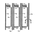
図1は電子デバイス100の一部分の回路図を含んでいる。電子デバイス100は第1の画素120、第2の画素140および第3の画素160を含んでいる。画素120、140、および160の各々は図1に示したような画素回路を含む。各画素回路は画素駆動回路および電子部品128、148、または168を含んでいる。
2. Circuit Diagram FIG . 1 includes a circuit diagram of a portion of
第1の画素120は選択トランジスタ122、容量性電子部品124、駆動トランジスタ126、および電子部品128を含む。電子部品128はほぼ、電流によって駆動される任意の電子部品であり得る。一実施形態では、電子部品128はOLEDなどの放射放出部品であるである。
The
画素120内では、画素駆動回路は選択トランジスタ122を含んでいる。選択トランジスタ122は選択ライン(「SL」)134に接続されたゲート電極、データライン(「DL」)132に接続された第1のソース/ドレイン領域、および容量性電子部品124の第1の電極に接続された第2のソース/ドレイン領域、および駆動トランジスタ126のゲート電極を含む。選択トランジスタ122が起動されると、SL134は制御信号を選択トランジスタ122に提供し、DL132は通過されるべきデータ信号を容量性電子部品124および駆動トランジスタ126のゲート電極に提供する。
Within the
画素駆動回路は容量性電子部品124も含む。容量性電子部品124は第1の電極および第2の電極を含む。容量性電子部品124の第1の電極は選択トランジスタ122の第2のソース/ドレイン領域および駆動トランジスタ126のゲート電極に接続される。容量性電子部品124の第2の電極はある実施形態ではVdd1ライン136である第1の電源ラインに接続される。別の実施形態(図示せず)では、任意の抗劣化ユニット(antidegradation unit)が容量性電子部品124および画素120に接続された電源ライン(例えば、Vssライン138、Vdd1ライン138、またはその両方)の少なくとも1つに接続されてよい。
The pixel drive circuit also includes a capacitive
画素駆動回路は駆動トランジスタ126をさらに含む。駆動トランジスタ126は第1のゲート電極、第1のソース/ドレイン領域、および第2のソース/ドレイン領域を含む。駆動トランジスタ126の第1のソース/ドレイン領域は電子部品128の第1の電極に接続されており、駆動トランジスタ126の第2のソース/ドレイン領域はVdd1ライン136に接続されている。
The pixel driving circuit further includes a driving
また画素駆動回路は電子部品128をさらに含む。電子部品128は第1の電極、およびVssライン138に接続された第2の電極を含む。一実施形態では、第1の電極はアノードであり、第2の電極はカソードである。別の実施形態では、電子部品128はOLEDなどの有機放射放出電子部品である。一実施形態では画素駆動回路である画素回路の残りの部分は、電子部品128を駆動するための可変電流減を提供するのによく適している。したがって、電子部品128の代わりか、または電子部品128と共に、電流で駆動される1つまたは複数の電子部品が使用されてよい。1つまたは複数の電子部品はダイオードを含んでよいか、または含まなくてもよい。
The pixel driving circuit further includes an
別の実施形態(図示せず)では、電子部品128および駆動トランジスタ126は逆であってよい。より具体的には、(1)電子部品128の第1の電極(例えば、アノード)はVdd1ライン136に接続され、(2)電子部品128の第2の電極(例えば、カソード)は駆動トランジスタ126のソース/ドレイン領域の一方に接続され、(3)駆動トランジスタ126の他方のソース/ドレイン領域はVssライン138に接続される。
In another embodiment (not shown), the
第2の画素140は第1の画素120に類似しているが、第2の画素140内では、データライン152は選択トランジスタ122の第1のソース/ドレイン領域に接続され、Vdd2ライン156は駆動トランジスタ126の第2のソース/ドレイン領域に接続され、電子部品148は駆動トランジスタ126の第1のソース/ドレイン領域とVssライン138との間に接続される。第3の画素160は第1および第2の画素120および140に類似しているが、第3の画素160内では、データライン172は選択トランジスタ122の第1のソース/ドレイン領域に接続され、Vdd3ライン176は駆動トランジスタ126の第2のソース/ドレイン領域に接続され、電子部品168は駆動トランジスタ126の第1のソース/ドレイン領域とVssライン138との間に接続される。
The
一実施形態では、電子部品128、148、168は互いに実質的に同じである。別の実施形態では、電子部品128、148、および168は互いに異なっている。例えば、電子部品128は青色発光部品であり、電子部品148は緑色発光部品であり、電子部品168は赤色発光部品である。Vdd1、Vdd2、およびVdd3ライン136、156、および176は互いに比較して同じ電圧または異なる電圧であってよい。別の実施形態(図示せず)では、電子部品128、148、168の第2の第2の電極は、実質的に同じ電圧または著しく異なる電圧で動作し得る異なる電源ラインに接続され得る。本願明細書を読めば、当業者は特定の用途のための要求または要望を満たすための電子デバイス100を設計することができよう。
In one embodiment, the
選択トランジスタ122、駆動トランジスタ126、またはそれらの任意の組合せは電界効果トランジスタを含むことができる。図1に示したような画素用の回路では、すべてのトランジスタはn−チャネルトランジスタである。n−チャネルトランジスタの任意の1つまたは複数は、任意の1つまたは複数のp−チャネルトランジスタに置き換えることができる。他の実施形態では、(JFETトランジスタまたはバイポーラトランジスタを含む)他のトランジスタが、選択トランジスタ122内で使用されてよい。
The
3.画素レイアウトおよび電子デバイス製造
図2〜14は図1に示したような回路の形成中の電子デバイスの一部の平面図および断面図の例示を含んでいる。この図面は電子部品および回路内のそれらの相互接続を形成するためのレイアウトおよび製造順序の2、3の実施形態を示しているに過ぎない。本願明細書を読めば、当業者は図1に示したような回路を形成する際に他のレイアウトが使用されてよいことを理解するであろう。わかりやすくするために、誘電体層および絶縁層は平面図に示していない。
3. Pixel Layout and Electronic Device Manufacturing FIGS. 2-14 include illustrations of top and cross-sectional views of a portion of an electronic device during the formation of a circuit as shown in FIG. This drawing shows only a few embodiments of the layout and manufacturing sequence for forming electronic components and their interconnections in the circuit. After reading this specification, one of ordinary skill in the art will appreciate that other layouts may be used in forming the circuit as shown in FIG. For clarity, the dielectric and insulating layers are not shown in the plan view.
図2および3は導電性部材222および224形成後のアレイ200の一部の平面図および断面図をそれぞれ示す。導電性部材222は2列の画素用の選択ライン134の部分である。図2の上部に近い方の導電性部材222は図1に示した画素用の選択ラインである。図2の下部の方に近い他の導電性部材222は形成される画素の下の列内の画素(図示せず)用の選択ラインである。活性領域によって次に被覆される導電性部材222の部分は、選択トランジスタ122用のゲート電極である。一実施形態では、導電性部材224は容量性電子部品124の第1の電極および駆動トランジスタ126用のゲート電極である。
2 and 3 show a top view and a cross-sectional view, respectively, of a portion of the
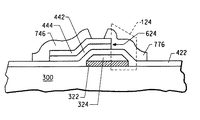
図3は、基板300の一部分およびライン3−3で切った所を見た導電性部材124の断面図の例示を含む。基板300は剛性または可撓性であり得、有機材料、無機材料または有機および無機両方の材料の1つまたは複数の層を含んでよい。一実施形態では、電子デバイスはボトムエミッションディスプレイを含み、基板300は基板300に入射する放射の少なくとも70%を該基板に通過させることを可能にする透明な材料を含む。
FIG. 3 includes an illustration of a cross-sectional view of the
導電性部材222よび224の各々は黒色層322および誘電体層324を含み、基板300の上に形成されている。一実施形態では、黒色層322および誘電体層324は従来の堆積順序および任意のパターンニング順序を用いて形成され得る。例えば、黒色層322および誘電体層324用の層は、ステンシルマスクを用いてパターン化層として堆積され得る。別の実施形態では、黒色層322および誘電体層324用の層は基板300の上に順次堆積されてよく、黒色層322および誘電体層324は従来のリソグラフィ法を用いてパターン化されてよい。さらに別の実施形態では、黒色層322は基板300の実質的に全体の上に形成されてよく、誘電体層324は黒色層322の上にパターン化層として堆積されてよい。誘電体層324はエッチング工程中にハードマスクとして働いて、誘電体層324によって被覆されていない黒色層322の部分を除去することができる。別の実施形態では、黒色層322は省かれてよく、誘電体層324は基板300の表面の上に形成されてよい。本願明細書を読めば、当業者は他の多くの技術が黒色層322および誘電体層324を形成する際に使用されてよいことを理解するであろう。
Each of the
黒色層322は環境光条件において使用されるときに、電子デバイスのコントラスト比の改善を可能にする。黒色層の材料および厚さは、Gang Yuらにより2004年5月7日に出願された「Array Comprising Organic Electronic Devices With a Black Lattice and Process For Forming the Same」という名称の特許文献1により完全に記載されている。一実施形態では、黒色層322はCr、Ni、またはその両方の1つまたは複数の層を含む。
The
誘電体層324は周期表の4〜6、8および10〜14族から選択される少なくとも1つの元素またはそれらの任意の組合せを含む1つまたは複数の層を含み得る。一実施形態では、誘電体層324はCu、Al、Ag、Au、Mo、またはそれらの任意の組合せを含むことができる。誘電体層324が2つ以上の層を含む別の実施形態では、その層の1つはCu、Al、Ag、Au、Mo、またはそれらの任意の組合せ含むことができ、別の層はMo、Cr、Ti、Ru、Ta、W、Si、またはそれらの任意の組合せを含むことができる。導電性金属酸化物、導電性金属窒化物、またはそれらの任意の組合せは、元素金属またはそれらの合金の代わりにまたはそれらと共に使用されてよい。一実施形態では、第1のゲート電極は約0.2〜5μmの範囲の厚さを有する。
誘電体層422、第1の半導体層442、および第2の半導体層444は、図4に示したように基板300および誘電体層324の上に順に形成される。誘電体層422、第1の半導体層442、および第2の半導体層444の各々は従来の堆積技術を用いて形成することができる。
The
誘電体層422は二酸化シリコン、アルミナ、酸化ハフニウム、窒化シリコン、窒化アルミニウム、酸窒化シリコン、半導体分野で使用されるような別の従来のゲート誘電体材料、またはそれらの任意の組合せを含んだ1つまたは複数の層を含むことができる。別の実施形態では、誘電体層422の厚さは約50〜1000nmの範囲にある。
第1および第2の半導体層442および444の各々は電子部品において半導体として従来使用される1つまたは複数の材料を含むことができる。一実施形態では、第1の半導体層442、第2の半導体層444、またはその両方は、アモルファスシリウコン(a−Si)、低温ポリシリコン(LTPS)、連続粒界シリコン(CGS)、またはそれらの任意の組合せとして形成(例えば、堆積)される。別の実施形態では、他の14族元素がそれ自身または組み合わせて(シリコンを含む場合または含まない場合)、第1の半導体層442、第2の半導体層444、またはその両方に使用されてよい。さらに他の実施形態では、第1および第2の半導体層442および444はIII−V族(13族−15族)半導体(例えばGaAs、InP、GaAlAs等)、II−VI族(2族−16族または12族−16族)半導体(例えば、CdTe、CdSe、CdZnTe、ZnSe、ZnTe、CuO等)、またはそれらの任意の組合せを含む。さらに別の実施形態では、第1および第2の半導体層442および444はポリアセチレン(PA)またはその誘導体のいずれも、ポリチオフェン(PT)またはその誘導体のいずれも、ポリ(p−フェニルビニレン)(PPV)またはMEH−PPVなどのその誘導体のいずれも、C60などのフラーレン分子またはその誘導体のいずれも、バッキーチューブ、アントラセン、テトラセン、ペンタセン、Alq3または他の金属キレート(M−L3)型有機金属分子、またはそれらの任意の組合せを含む。第1および第2の半導体層442および444のいずれかまたは両方はまた、有機材料および無機材料を含んだ複合物であり得るか、またはそのような材料の二重層または多層の形態であり得る。
Each of the first and second semiconductor layers 442 and 444 can include one or more materials conventionally used as semiconductors in electronic components. In one embodiment, the
一実施形態では、第1の半導体層442は唯一の半導体材料としてシリコンを含み、第2の半導体層444はゲルマニウム、シリコンゲルマニウム、またはシリコン単独と異なるか、またはシリコンと混合された別の半導体材料を含む。第1および第2の半導体層442および444内に異なる材料が存在することの有意さは、本願明細書において後で記載されるようにパターンニング順序に明らかとなろう。
In one embodiment, the
第1の半導体層442はドープされていないか、または約1×1019個の原子/cm3以下の濃度のn型またはp型のドーパントを有する。第2の半導体層444は第1の半導体層442よりも重い濃度でn型またはp型のドーパントを含む。一実施形態では、次に形成される金属含有構造体とのオーミックコンタクトを形成するために、第2の半導体層444は、少なくとも1×1019個の原子/cm3までn+またはp+にドープされている。別の実施形態では、第2の半導体層444内のドーパント濃度は1×1019個の原子/cm3未満であり、次に形成される金属含有構造体と接するときにショットキーコンタクトを形成する。従来のn型ドーパント(例えば、リン、ヒ素、アンチモン等)またはp型ドーパント(ホウ素、ガリウム、アルミニウム等)を使用することができる。このようなドーパントを堆積中に組み入れることができるか、または別個のドーピング順序(例えば、注入またはアニーリング)中に添加することができる。第1および第2の半導体層442および444は従来の堆積およびドーピング技術を用いて形成される。一実施形態では、第1の半導体層442の厚さは約30〜550nmの範囲であり、第2の半導体層444の厚さは約50〜500nmの範囲にある。本願明細書を読めば、当業者は他の厚さを用いて駆動トランジスタ126の所望の電子的特性を達成され得ることを理解するであろう。
The
図5に示すように、第1および第2の半導体層442および444をパターン化して、選択トランジスタ122および駆動トランジスタ126用の活性領域522および526が形成される。続いて、活性領域522および526を順次パターン化して、選択トランジスタ122および駆動トランジスタ126用のチャネル領域およびソース/ドレイン領域が定められる。
As shown in FIG. 5, the first and second semiconductor layers 442 and 444 are patterned to form
第1および第2の半導体層442および444は従来のリソグラフィ技術を用いてパターン化される。図6の構造体は1対の端部622および624を有している。第1および第2の半導体層442および444は、端部622および624の各々において同一境界であることに留意されたい。別の実施形態では、第1および第2の半導体層442および444はステンシルマスクを用いてパターン化層として堆積されて、図6に示すようにパターン化された第1および第2の半導体層442および444を形成する。誘電体層324の一部は図6の端部624の右に延びていることに留意されたい。誘電体層324のその部分は容量性電子部品124用の第1の電極である。端部624の右に延びかつ誘電体層324と接する誘電体層422の部分は、容量性電子部品124用のキャパシタ誘電体層である。端部624の左に延びかつ誘電体層324と接する誘電体層422の部分は、駆動トランジスタ126用のゲート誘電体層である。
The first and second semiconductor layers 442 and 444 are patterned using conventional lithography techniques. The structure of FIG. 6 has a pair of
導電性部材732、736、744、746、752、756、772、および776は図7に示したように基板300の上に形成される。図7では、導電性部材732、736、744、746、752、756、772、および776間の位置関係をわかりやすくするために下側の層は示していない。導電性部材732はデータライン132の一部であり、部分734を含んでいる。図7の上部に近い方の導電性部材732の部分734は画素120内の選択トランジスタ122用の第1のソース/ドレインコンタクト構造体である。他方の部分734は画素120の下の画素(図示せず)内の選択トランジスタ122用の第1のソース/ドレインコンタクト構造体である。導電性部材752はデータライン152の一部であり、部分754を含んでいる。図7の上部に近い方の導電性部材752の部分754は画素140内の選択トランジスタ122用の第1のソース/ドレインコンタクト構造体である。他方の部分754は画素140の下の画素(図示せず)内の選択トランジスタ122用の第1のソース/ドレインコンタクト構造体である。導電性部材772はデータライン172の一部であり、部分774を含んでいる。図7の上部に近い方の導電性部材772の部分774は画素160内の選択トランジスタ122用の第1のソース/ドレインコンタクト構造体である。他方の部分774は画素160の下の画素(図示せず)内の選択トランジスタ122用の第1のソース/ドレインコンタクト構造体である。
導電性部材744は選択トランジスタ122用の第2のソース/ドレインコンタクト構造体である。導電性部材746は駆動トランジスタ126用の第1のソース/ドレインコンタクト構造体である。導電性部材736はVdd1ライン136用の一部であり、導電性部材756はVdd2ライン156用の一部であり、導電性部材776はVdd3ライン176の一部である。
図8を参照すると、端部624の右に存在する導電性部材776の部分は、画素160内の容量性電子部品124用の第2の電極である。端部624の左に存在する導電性部材776の部分は、画素160内の駆動トランジスタ126の第2のソース/ドレイン領域用のコンタクト構造体の一部である。図8において点線で示した容量性電子部品124は、端部624の右に存在する誘電体層324、誘電体層422、および導電性部材776の一部を含んでいる。画素120および140用の容量性電子部品124は類似する構造を有している。導電性部材736および756の一部は、それぞれ画素120および140の容量性電子部品用の第2の電極である。
Referring to FIG. 8, the portion of the
導電性部材732、736、744、746、752、756、772、および776は従来の技術を用いて形成することができる。一実施形態では、堆積工程中にステンシルマスクを用いて、導電性部材732、736、744、746、752、756、772、および776が形成されてよい。別の実施形態では、導電性部材732、736、744、746、752、756、772、および776は基板300の実質的に全体の上に1つまたは複数の層を堆積させ、かつ従来のリソグラフィ技術を用いてその層をパターン化することによって形成される。誘電体層324に関して記載した材料および厚さの任意のものが導電性部材732、736、744、746、752、756、772、および776に使用されてよい。一実施形態では、導電性部材732、736、744、746、752、756、772、および776は誘電体層324と実質的に同じ組成および厚さを有する。別の実施形態では、導電性部材732、736、744、746、752、756、772、および776は誘電体層324と比べて異なる組成、厚さ、またはその両方を有する。
図7を参照すると、電子デバイスの平面図によれば、第2の半導体層444の露出部分(図7で示さず)は、(1)導電性部材744と導電性部材732の一部分734との間、(2)導電性部材744と導電性部材752の一部分754との間、(3)導電性部材744と導電性部材772の一部分774との間、(4)導電性部材746と導電性部材736との間、(5)導電性部材746と導電性部材756との間、および(6)導電性部材746と導電性部材776との間の各々に存在する。
Referring to FIG. 7, according to the plan view of the electronic device, the exposed portion (not shown in FIG. 7) of the
一実施形態では、第2の半導体層444上の導電性部材間の間隔の各々は、使用される設計基準のほぼ最小寸法である。一実施形態では、4μmの設計基準が使用される場合、間隔は各々約4μmである。別の実施形態では、この間隔は設計基準の最小寸法以上である。本願明細書を読めば、当業者は特定のトランジスタ設計の要求または要望を最も満たすドレインコンタクトとソースコンタクトの間の間隔を選択することができる。
In one embodiment, each of the spacing between conductive members on the
次に、第2の半導体層444の露出部分を除去して、図9に示したような第2の半導体層444を通って延びる開口部902が形成される。この実施形態では、導電性部材746および776は第2の半導体層444の露出部分を除去するときにハードマスクの一部となる。第2の半導体層844の残りの部分は相互に離間されており、選択トランジスタ122および駆動トランジスタ126用のソース/ドレイン領域である。第3の画素160内では、駆動トランジスタ126用のチャネル領域は導電性部材746および776に対して自己整列している。他の駆動トランジスタ126および選択トランジスタ122用のチャネル領域922が、実質的に同時間に実質的に同じ様式で形成される。選択トランジスタ122および駆動トランジスタ126はアンダーゲートTFTである。これはそのトランジスタ用のゲート電極がそれに対応するチャネル領域922の下にあるためである。導電性部材722と選択トランジスタ122および駆動トランジスタ126の重なっているチャネル領域922との間に存在する誘電体層422の部分は、選択トランジスタ122および駆動トランジスタ126用のゲート誘電体層である。
Next, the exposed portion of the
チャネル領域922の物理的チャネル長924の各々は、開口部902に沿った第2の半導体層444の部分間の距離である。一実施形態では、物理的チャネル長924の1つまたは複数は設計基準の最小寸法の僅か2倍である。別の実施形態では、物理的チャネル長924の1つまたは複数は設計基準の最小寸法の僅か1.2倍である。別の実施形態では、物理的チャネル長924は上記よりも大きくてよいか、または小さくてもよい。
Each of the
第2の半導体層444のエッチングはウェットエッチングまたはドライエッチング法を用いて行われてよい。一実施形態では、導電性部材732、736、744、746、752、756、772、および776に関して第2の半導体層444を選択的(すなわち、より高い率のエッチング)に除去することができるように、エッチング剤を選択することができる。
Etching of the
一実施形態では、ハロゲンを含んだプラズマを用いてドライエッチング法を実行することによって、第2の半導体層444の露出部分が除去されてよい。供給ガスはフッ素含有ガスなどのハロゲン含有ガスを含むことができる。このハロゲン含有ガスは化学式CaXbHcを有することができる。ここで、Xは1つまたは複数のハロゲンであり、aは1または2であり、bは少なくとも1であり、aが1の場合にはb+cは4でaが2の場合にはb+cは4または6である。例えば、XがFのとき、ハロゲン含有ガスはフルオロカーボンである。別の実施形態では、フッ素含有ガスはF2、HF、SF6、NF3、フッ素含有ハロゲン間化合物(CIF、CIF3、CIF5、BrF3、BrF5、およびIF5)、またはそれらの任意の混合物を含むことができる。別の実施形態では、ハロゲン含有ガスはCl2、HCl、BCl3を含む塩素含有ガス、塩素含有ハロゲン間化合物(CIF、CIF3、およびCIF5)、またはそれらの任意の混合物である。さらに別の実施形態では、ハロゲン含有ガスはBr2、HBr、BBr3を含む臭素含有ガス、臭素含有ハロゲン間化合物(BrF3およびBrF5)、またはそれらの任意の混合物である。さらに別の実施形態では、ハロゲン含有ガスはI2を含むヨウ素含有ガス、HI、またはそれらの任意の混合物である。またさらに別の実施形態では、ハロゲン含有ガスはこのパラグラフに記載したガスの任意の混合物である。具体的な実施形態では、第2の半導体層444と第1の半導体層442との間のエッチング選択性(すなわち、第2の半導体層444のエッチング速度と第1の半導体層442のエッチング速度との比)は、フッ素に比べてより重いハロゲンをより多く用いることによって改善することができる。例えば、エッチング選択性はyが大きくなるにしたがってCF(1−y)Clyと共に改善する。
In one embodiment, the exposed portion of the
供給ガスはO2、O3、N2Oなどの任意の1つまたは複数の酸素含有ガス、または半導体分野において酸素プラズマを精製するのに従来使用される他の酸素含有ガスを含むことができる。供給ガスは1つまたは複数の不活性ガス(例えば、希ガス、N2、CO2、またはそれらの任意の組合せ)も含むことができる。 The feed gas can include any one or more oxygen-containing gases such as O 2 , O 3 , N 2 O, or other oxygen-containing gases conventionally used to purify oxygen plasma in the semiconductor field. . The feed gas can also include one or more inert gases (eg, noble gases, N 2 , CO 2 , or any combination thereof).
エッチングはエッチング室内で実行することができる。エッチング中、その圧力は約0.01〜5000mトールの範囲にある。このような圧力で、供給ガスは約10〜1000標準立方センチメートル/分(「sccm」)の範囲の速度で流れ得る。別の実施形態では、この圧力は約100〜500mトールの範囲であってよく、供給ガスは約100〜500sccmの範囲の速度で流れてよい。電圧および出力を印加してプラズマが発生され得る。出力は典型的には、基板の表面積の線形関数またはほぼ線形関数である。したがって、出力密度(基板の単位面積当たりの出力)が得られる。電圧は約10〜1000Vの範囲であり、出力密度は約10〜5000mW/cm2の範囲である。一実施形態では、電圧は約20〜300Vの範囲であってよく、出力密度は約50〜500mW/cm2の範囲であってよい。 Etching can be performed in an etching chamber. During etching, the pressure is in the range of about 0.01 to 5000 mTorr. At such pressures, the feed gas may flow at a rate in the range of about 10 to 1000 standard cubic centimeters per minute (“sccm”). In another embodiment, the pressure may range from about 100 to 500 mTorr and the feed gas may flow at a rate in the range of about 100 to 500 sccm. A plasma can be generated by applying a voltage and power. The output is typically a linear or nearly linear function of the surface area of the substrate. Therefore, output density (output per unit area of the substrate) is obtained. The voltage is in the range of about 10 to 1000 V, and the power density is in the range of about 10 to 5000 mW / cm 2 . In one embodiment, the voltage may be in the range of about 20-300V and the power density may be in the range of about 50-500 mW / cm 2 .
エッチングは時限式エッチングとして、または時限式のオーバーエッチングと共に終点検出を用いることによって実行されてよい。第1および第2の半導体層442および444が大部分シリコンの場合、時限式エッチングが使用されてよい。第1および第2の半導体層442および444に異なる材料が使用される場合、終点検出が使用されてよい。例えば、一実施形態では、第2の半導体層444がシリコンゲルマニウムを含む場合、終点検出は第1の半導体層442が露出された後にエッチング室からの排出物中にゲルマニウムが存在しないことに基づくものであってよい。別の実施形態では、第2の半導体層444が殆どシリコンを有さないゲルマニウムを含む場合、終点検出は第1の半導体層442が露出された後にエッチング室からの排出物中にシリコンが存在することに基づくものであってよい。時限式オーバーエッチングを用いて、第2の半導体層444の部分をエッチングがよりゆっくりと発生する基板300の領域から除去されることを確実にしてよい。一実施形態では、エッチング中の出力密度をオーバーエッチング中に低減させて、第1の半導体層442に対する第2の半導体層444およびエッチングプラズマに曝露される電子デバイスの他の部分の選択性が改善されてよい。
The etching may be performed as a timed etch or by using endpoint detection with a timed overetch. If the first and second semiconductor layers 442 and 444 are mostly silicon, a timed etch may be used. If different materials are used for the first and second semiconductor layers 442 and 444, endpoint detection may be used. For example, in one embodiment, when the
選択される湿式化学エッチング剤は一部には第2の半導体層444の組成およびエッチング中に露出される電子デバイスの他の部分に基づくであろう。一実施形態では、エッチング剤は基剤(例えば、KOH、水酸化テトラメチルアンモニウム等)、または酸化剤(例えば、HNO3)およびHFの組合せを含むことができる。湿式化学エッチングには時限式のエッチングが典型的に使用される。
The wet chemical etchant selected will be based in part on the composition of the
エッチング終了後、第1の半導体層442の一部が除去されてよいか、または一切除去されなくてもよい。一実施形態では、第1の半導体層442の僅か約50nmが除去される。
After the etching is completed, part of the
工程のこの時点では、画素駆動回路内の電子部品の形成は実質的に完了している。図9を参照すると、画素160内では、端部624の左の誘電体層324の部分は駆動トランジスタ126用のゲート電極を含む。端部624の右の誘電体層324の部分は容量性電子部品124用の第1の電極である。導電性部材746の下にある第2の半導体層444の部分は駆動トランジスタ126用の第1のソース/ドレイン領域であり、導電性部材776の下にある第2の半導体層444の部分は駆動トランジスタ126用の第2のソース/ドレイン領域である。開口部902内の露出した第1の半導体層の部分は駆動トランジスタ126のチャネル領域である。端部624の右の導電性部材776の部分は容量性電子部品124用の第2の電極である。他の画素120および140内の他の駆動トランジスタ126および容量性電子部品124は、図9に示したものと実質的に同一である。
At this point in the process, the formation of the electronic components in the pixel drive circuit is substantially complete. Referring to FIG. 9, in the
絶縁層および絶縁層内の開口部は基板300の部分の上に形成される。導電性部材1022および1024は図10に示したように基板300の部分の上に形成される。導電性部材1022は電子部品128、148、および168用の第1の電極であり、下側の導電性部材746に接続されている。画素120、140、および160内では、導電性部材1024は導電性部材744および導電性部材224に接続されている。導電性部材1024は選択トランジスタ122の第2のソース/ドレイン領域を駆動トランジスタ126のゲート電極および容量性電子部品124の第1の電極に接続するためのローカルな相互接続である。
The insulating layer and the opening in the insulating layer are formed on a portion of the
工程のこの時点では、画素駆動回路が形成され、選択トランジスタ122、容量性電子部品124、および駆動トランジスタ126を含んでいる。図10を参照すると、選択トランジスタ122の長さは選択ライン134でもある導電性部材222の長さと実質的に平行であり、図10に示したように横に延在している。容量性電子部品124および駆動トランジスタ126の長さは導電性部材736、756、および776の長さと実質的に平行である。選択トランジスタ122、容量性電子部品124および駆動トランジスタ126の各々に関し、電子デバイスの平面図からわかるように、その長さはそれに対応する幅よりも長い。一実施形態では、容量性電子部品124の長さは駆動トランジスタ126の長さよりも長い。別の実施形態では、容量性電子部品124の長さは駆動トランジスタ126の長さより短いか、または実質的にそれと同じである。
At this point in the process, a pixel drive circuit is formed and includes a
平面図によれば、各画素120、140、および160内では、駆動トランジスタ126および容量性電子部品124は、駆動トランジスタ126および容量性電子部品124の長さに実質的に平行なラインに沿って相互に実質的に同一境界である。一実施形態では、このラインは図9に示したような端部624に相当する。駆動トランジスタ126は端部624の左に存在し、容量性電子部品124は端部624の右に存在する。本願明細書で用いられるように、図9および10に示したように、同一境界は相互に接する物理的に異なる構造を含むことができるか、またはラインにわたって延在する物理的に異なる構造を含むことができる。より具体的には、導電性部材224、誘電体層422、および端部624の左の導電性部材776の一部は、画素160内の駆動トランジスタ126用のパーツまたはコンタクト構造体である。導電性部材224、誘電体層422、および端部624の右の導電性部材776の一部は、画素160内の容量性電子部品124用のパーツまたはコンタクト構造体である。導電性部材224、誘電体層422、および導電性部材776の各々は、端部624にわたって連続的に延びている。したがってm容量性電子部品124および駆動トランジスタ126は画素160内で実質的に同一境界である。他の画素120および140は実質的に同一の形状を有する。
According to the plan view, within each
各画素120、140、および160内では、選択トランジスタ122の長さは画素の第1の側に沿って存在し、駆動トランジスタ126の長さは画素の第2の側に沿って存在する。具体的な一実施形態では、画素の第1の側の各々は画素の第2の側の各々に対して実質的に平行である。別の具体的な実施形態では、駆動トランジスタ126の長さは画素の第2の側の長さの少なくとも半分である。一実施形態では、駆動トランジスタの長さは画素の第2の側の長さの70%を超えて延在し、より具体的な実施形態では、画素の第2の側の長さの85%を超えて延在する。
Within each
図11は図10のライン11−11で切った断面図を含んでおり、導電性部材1022および1024を形成後の電子デバイスの構成である。絶縁層1122および絶縁層1122内の開口部は1つまたは複数の従来の技術を用いて形成することができる。一実施形態では、絶縁層1122はステンシルマスクを用いてパターン化層として堆積される。別の実施形態では、絶縁層1122は基板300の実質的に全体の上にブランケット堆積(blanket deposited)され得、かつ従来のリソグラフィ技術を用いてパターン化され得る。絶縁層1122は誘電体層422に関して先に記載した材料のいずれかの1つまたは複数の層を含むことができる。絶縁層1122の厚さは約0.1〜5.0μmの範囲にある。
FIG. 11 includes a cross-sectional view taken along line 11-11 in FIG. 10 and shows the configuration of the electronic device after the
導電性部材1022および1024は従来のOLEDにおいてアノードに従来使用される1つまたは複数の材料の1つまたは複数の層を含むことができる。導電性部材1022および1024は従来の堆積を用いて、または従来の堆積およびパターンニング順序によって形成することができる。
一実施形態では、導電性部材1022は次に形成される有機活性層から放出される、またはそれによって応答される放射の少なくとも70%を伝達する。一実施形態では、導電性部材1022および1024の厚さは約100〜200nmの範囲である。放射が導電性部材1022および1024を透過する必要がないのであれば、もっと厚くてよく、例えば1000nmまで、あるいはさらに厚くてよい。
In one embodiment, the
基板構造体1222は図12に示したように画素駆動回路の上に形成される。一実施形態では、基板構造体1222は井戸構造であり、別の実施形態では、基板構造体1222は液体ガイド構造体であり得る(すなわち、格子ではなくストリップ形態の形状を有する)。一実施形態では、基板構造体1222の少なくとも部分は電子部品128、148、168、またはそれらの任意の組合せと、選択トランジスタ122および駆動トランジスタ126の少なくとも一部分との間に存在する(例えば、選択トランジスタ122および駆動トランジスタ126の少なくとも半分)。別の実施形態では、選択トランジスタ122および駆動トランジスタ126ならびに容量性電子部品124を含む画素駆動回路の実質的にすべては、基板構造体1222によって被覆される。さらに別の実施形態では、選択トランジスタ122および駆動トランジスタ126のチャネル領域は基板構造体1222によって被覆される。
The
図13は図12のライン13−13で切った断面図を含んでおり、基板構造体1222の一部と画素160内の下側の駆動トランジスタ126および容量性電子部品124との間の位置関係を示している。基板構造体1222は基板300および導電性部材1022の部分の上に重なっている。基板構造体1222は、放射が次に形成される有機活性層へ送られ得るか、またはそこから送られ得る開口部のアレイを定めている。基板構造体1222内の開口部は導電性部材1022の部分を露出する。
FIG. 13 includes a cross-sectional view taken along line 13-13 in FIG. 12, and the positional relationship between a portion of the
具体的な実施形態では、基板構造体1222は無機材料(例えば、二酸化シリコン、窒化シリコン、酸化アルミニウム、窒化アルミニウム等)または有機材料(例えば、フォトレジスト、ポリイミド等)、またはそれらの任意の組合せを含む。別の実施形態では、電子デバイスが操作されている間に環境光に対するコントラストを増大させるために基板構造体122は黒色層(例えば、炭素を含む層)を含むことができる。例示的な一実施形態では、基板構造体1222は1つまたは複数のレジスト層またはポリマー層から形成されてよい。このレジストは、例えば、ネガ型レジスト材料またはポジ型レジスト材料であってよい。
In a specific embodiment, the
レジストは従来の技術を用いて基板300および導電性部材1022の上に堆積することができる。基板構造体1222は堆積されたものとしてパターン化されてよいか、またはブランケット層として堆積されかつ従来のリソグラフィ技術を用いてパターン化されてよい。特定の一実施形態では、基板構造体1222は断面図から見て約2〜10μmの厚さを有する。例示的な一実施形態では、基板構造体1222内の開口部は平面図から見て、約50〜100μmの範囲の幅および約100〜500μmの範囲の長さである。開口部の基板構造体1222の傾斜は導電性部材1022の表面に対して90°未満、約90°、または90°超である。
The resist can be deposited on the
一実施形態では、次の有機層を形成する前に、基板構造体1222は表面処理を受けてよいか、または受けなくてもよい。従来のフッ素化表面処理を行って基板構造体1222の表面エネルギが低減されてよい。
In one embodiment, the
処理を続けて図14に示したような実質的に完成された電子部品を形成する。有機層1430および第2の電極1442が基板300の上に形成される。有機層1430は1つまたは複数の層を含んでよい。有機層1430は有機活性層1434を含み、任意には、電荷注入層、電荷輸送層、電荷阻止層、またはそれらの任意の組合せのうち任意の1つまたは複数を含んでよい。任意の電荷注入層、電荷輸送層、電荷阻止層、またはそれらの任意の組合せは、有機活性層1434と導電性部材1022との間、有機活性層1434と第2の電極1442との間、またはそれらの組合せの間に存在してよい。一実施形態では、正孔輸送層1432は導電性部材1022と有機活性層1434との間に存在する。
Processing continues to form a substantially completed electronic component as shown in FIG. An organic layer 1430 and a
有機層1430の形成は、OLEDにおいて有機層を形成する際に使用される任意の1つまたは複数の技術を用いて実行される。正孔輸送層1432は約50〜200nmの範囲の厚さを有し、有機活性層1434は約50〜100nmの範囲の厚さを有する。一実施形態では、唯一の有機活性層がアレイにおいて用いられる。別の実施形態では、異なる有機活性層がアレイ内の異なる部分において用いられてよい。
Formation of the organic layer 1430 is performed using any one or more techniques used in forming organic layers in OLEDs. The
第2の電極1442は従来のOLEDにおいてカソードに使用される1つまたは複数の材料の1つまたは複数の層を含む。第2の電極1442は1つまたは複数の従来の堆積技術ならびに従来の堆積およびリソグラフィ技術を用いて形成される。一実施形態では、第2の電極1442は約0.1〜5.0μmの範囲の厚さを有する。具体的な実施形態では、第2の電極1442はアレイ用の共通のカソードであり得る。
The
図14に示していない他の回路は、任意の数の先に記載した層または付加的な層を用いて形成されてよい。図示していないが、付加的な絶縁層および相互接続レベルはアレイの外部に存在し得る周辺領域(図示せず)において回路を可能にするように形成されてよい。そのような回路は列デコーダまたは行デコーダ、ストローブ(例えば、列アレイストローブ、行アレイストローブ)、またはセンス増幅器を含んでよい。別の場合には、そのような回路は図14に示した任意の層の形成前、形成中、または形成後に形成されてよい。一実施形態では、第2の電極1442はVssライン138の一部である。
Other circuits not shown in FIG. 14 may be formed using any number of previously described layers or additional layers. Although not shown, additional insulating layers and interconnect levels may be formed to allow circuitry in peripheral regions (not shown) that may exist outside the array. Such circuits may include column or row decoders, strobes (eg, column array strobes, row array strobes), or sense amplifiers. In other cases, such circuitry may be formed before, during, or after the formation of any of the layers shown in FIG. In one embodiment, the
乾燥剤1464を有する蓋1462を基板300のアレイ外部の場所(図14には示さず)に取り付けて、実質的に完成されたデバイスを形成する。空隙1466が第2の電極1442と乾燥剤1464との間にあってもよいか、またはなくてもよい。蓋および乾燥剤に使用される材料ならびに取付け方法は従来のものである。
A
4.他の実施形態
上記実施形態は単色ディスプレイまたはフルカラーディスプレイを含むAMOLEDディスプレイによく適している。さらに、本願明細書に記載の概念を他のタイプの放射放出電子部品に使用することができる。他の放射放出電子部品はIII−V族またはII−VI族ベースの無機放射放出部品などの、受動マトリスディスプレイ光パネル、無機LEDを含むことができる。一実施形態では、放射放出電子部品は可視光スペクトル内にある放射を放出してよく、別の実施形態では、放射放出電子部品は可視光スペクトル外の放射(例えば、UVまたはIR)を放出してよい。
4). Other Embodiments The above embodiments are well suited for AMOLED displays including single color displays or full color displays. Furthermore, the concepts described herein can be used for other types of radiation-emitting electronic components. Other radiation emitting electronic components can include passive matrix display light panels, inorganic LEDs, such as III-V or II-VI based inorganic radiation emitting components. In one embodiment, the radiation emitting electronic component may emit radiation that is in the visible light spectrum, and in another embodiment, the radiation emitting electronic component emits radiation outside the visible light spectrum (eg, UV or IR). It's okay.
別の実施形態では、本願明細書に記載の概念は他のタイプの電子デバイスに拡大されてよい。一実施形態では、センサアレイは放射応答電子部品のアレイを含んでよい。一実施形態では、異なる放射応答電子部品は同じかまたは異なる活性材料を有してよい。このような活性材料の応答は経時的に変化してよい。さらに、センサアレイの一部は、種々の波長、種々の放射強度、またはそれらの組合せを受け取る種々の部分を含んでよい。放射放出電子部品を有する電子デバイスと同様、放射応答電子部品を有する電子デバイスの寿命は、より長い耐用寿命を有し得る。 In other embodiments, the concepts described herein may be extended to other types of electronic devices. In one embodiment, the sensor array may include an array of radiation responsive electronic components. In one embodiment, the different radiation responsive electronic components may have the same or different active materials. The response of such active materials may change over time. Further, a portion of the sensor array may include various portions that receive various wavelengths, various radiation intensities, or combinations thereof. Similar to electronic devices having radiation-emitting electronic components, the lifetime of an electronic device having radiation-responsive electronic components can have a longer useful life.
放射は基板300、蓋1462、またはその両方を透過され得る。蓋1462に放射を透過させる場合、蓋は放射の少なくとも70%を透過させるであろう。乾燥剤1464は放射が蓋1462を介して有機活性層1434から放出されるかまたはそれによって受け取られるように、放射の少なくとも70%を透過させるように修正され得る。例えば、乾燥剤は有機活性層1434ではなく、基板構造体1322の上に重なってよい。別の実施形態では、導電性部材1022および1442の組成は逆であってよい。この実施形態では、カソードは共通のアノードに比べて基板300に近い。画素駆動回路および発光部品間の相互接続はそのような構造体のために変形されてよい。
The radiation may be transmitted through the
容量性電子部品124の容量は導電性部材224の任意の1つまたは複数とそれに重なる導電性部材736、756、または776との間の重なりにおいて増大または低減され得る。例えば、容量性電子部品124の一部である導電性部材224、736、756、776、またはそれらの任意の組合せの部分は、図9および10に示したものに比べ、狭い、幅広い、長い、または短いものであってよい。容量性電子部品124の容量の変更は駆動トランジスタ126と別個になされてよいか、またはなされなくてもよいことに留意されたい(例えば、駆動トランジスタ126内にあるか、駆動トランジスタ126とのコンタクト構造体である導電性部材224、736、756、776、またはそれらの任意の組合せの部分)。
The capacitance of the capacitive
同じく、駆動トランジスタ126の電子的特性は活性領域526の長さ(例えば、活性領域526の長さ)を変えることによって変更され得る。駆動トランジスタ126の電子的特性の変化は容量性電子部品124と別個になされてよいか、またはなされなくてもよいことに留意されたい(例えば、容量性電子部品124の一部である導電性部材224、736、756、776、またはそれらの任意の組合せの部分)。
Similarly, the electronic characteristics of the
厚さ、幅、および長さを含む多くの寸法をいくつかの実施形態に関して記載した。本発明の範囲はその寸法または寸法の範囲に限定されるものではない。本願明細書を読めば、当業者は他の寸法を用いることができることを理解するであろう。 Many dimensions have been described for some embodiments, including thickness, width, and length. The scope of the invention is not limited to that dimension or range of dimensions. After reading this specification, one of ordinary skill in the art will appreciate that other dimensions can be used.
5.利点
本願明細書に記載のレイアウトおよび電子部品構造体は、画素内の空間をより有効に使用して、従来の画素に比べて画素の開口率を増大できるようにする。一実施形態では、各画素内では、容量性電子部品124および駆動トランジスタ126は相互に実質的に同一境界である。そのような構成によって、最小寸法の分離を容量性電子部品124と駆動トランジスタ126との間で維持する必要がないので、画素駆動回路が画素内で占める面積をより小さくすることが可能となる。また、選択トランジスタ122および駆動トランジスタ126の長さは画素の異なる側に沿っている。
5. Advantages The layout and electronic component structure described herein allows more efficient use of space within a pixel to increase the aperture ratio of the pixel compared to conventional pixels. In one embodiment, within each pixel, capacitive
少なくとも40%の開口率が達成され得る。一実施形態では、開口率は少なくとも50%であり、具体的な一実施形態では、開口率は約53%であり、さらにより具体的な実施形態では、開口率は約55%である。このような開口率は従来のボトムエミッション有機電子デバイスでは達成されなかった。開口率が大きくなれば、駆動トランジスタ126および電子部品128、148および168を含む画素回路をより弱い条件(すなわち、低い電流)で動作させることができ、さらに所望の強度を得ることができる。電流を低減させれば、駆動トランジスタ126および電子部品128、148、および168が急速には劣化されないので、電子デバイスの寿命が延びる。
An aperture ratio of at least 40% can be achieved. In one embodiment, the aperture ratio is at least 50%, in one specific embodiment, the aperture ratio is about 53%, and in an even more specific embodiment, the aperture ratio is about 55%. Such an aperture ratio has not been achieved with conventional bottom emission organic electronic devices. When the aperture ratio is increased, the pixel circuit including the driving
一般的な説明または実施形態に記載したすべての行為が必要というわけではなく、特定の行為の一部は必要とされなくてよく、また上記のものに加えてさらなる行為が行われてよいことに留意されたい。またさらに、行為の各々が列挙された順序は、必ずしもそれが実行される順序ではい。本願明細書を読めば、当業者は自分の特定の必要性または要望にどの行為を使用することができるかを決定することができる。 Not all actions described in the general description or embodiments are required, some of the specific actions may not be required, and further actions may be performed in addition to the above. Please keep in mind. Still further, the order in which each act is listed is not necessarily the order in which it is performed. After reading this specification, one skilled in the art can determine which actions can be used for his particular needs or desires.
上記明細書では、具体的な実施形態を参照して本発明を記載した。しかし、当業者は種々の変形および変更が添付の特許請求の範囲に記載の本発明の範囲から逸脱することなくなされ得ることを理解する。したがって、本明細書および図面は限定的意味ではなく例示的なものとみなされるべきであり、そのような変形はすべて本発明の範囲に含まれることが意図される。 In the foregoing specification, the invention has been described with reference to specific embodiments. However, one of ordinary skill in the art appreciates that various modifications and changes can be made without departing from the scope of the present invention as set forth in the claims below. The specification and drawings are, accordingly, to be regarded in an illustrative rather than a restrictive sense, and all such modifications are intended to be included within the scope of the present invention.
任意の1つまたは複数の有利、1つまたは複数の他の利点、1つまたは複数の問題に対する1つまたは複数の解決策、またはそれらの任意の組合せを、1つまたは複数の具体的な実施形態に関して記載してきた。しかし、有利、利点、問題に対する解決策、または任意の有利、利点、または解決策を想起させ得るか、または顕著にさせ得る任意の要素は、添付の特許請求の範囲の決定的、必要な、または不可欠な特徴または要素であると解釈されるべきではない。 One or more specific implementations of any one or more advantages, one or more other advantages, one or more solutions to one or more problems, or any combination thereof The form has been described. However, any element that may cause or make an advantage, advantage, solution to a problem, or any advantage, advantage, or solution conspicuous, is essential to the appended claims, Or should not be construed as essential features or elements.
明確にするために別個の実施形態に関連して上および下に記載した本発明の特定の特徴は、単一の実施形態として組み合わせて提供されてもよいことを理解されたい。逆に、簡略化するために単一の実施形態に関連して記載される本発明の特徴は、別個または任意の副結合で提供されてもよい。さらに、範囲の点で記載した値の参照は、その範囲内のすべての値を含む。 It should be understood that certain features of the invention described above and below in connection with separate embodiments for clarity may be provided in combination as a single embodiment. Conversely, features of the invention described in connection with a single embodiment for simplicity may be provided separately or in any subcombination. Further, reference to values stated in terms of ranges include all values within that range.
Claims (10)
前記画素は、
アンダーゲートTFTであり、かつ第1の導電性部材の第1の部分は第1のトランジスタのゲート電極である第1のトランジスタと、
前記第1の導電性部材の第2の部分は容量性電子部品の第1の電極である容量性電子部品と
を具えたことを特徴とする画素を含んだ有機電子デバイス。 An organic electronic device including pixels,
The pixel is
A first transistor that is an under-gate TFT and the first portion of the first conductive member is a gate electrode of the first transistor;
An organic electronic device including a pixel, wherein the second portion of the first conductive member includes a capacitive electronic component that is a first electrode of the capacitive electronic component.
前記第2の導電性部材の第2の部分は、前記容量性電子部品の第2の電極であることを特徴とする請求項1記載の有機電子デバイス。 The first part of the second conductive member is a contact structure of the source / drain region of the first transistor, and the second part of the second conductive member is the capacitive electronic component The organic electronic device according to claim 1, wherein the second electrode is a second electrode.
前記第1の層の第2の部分は、前記容量性電子部品用のキャパシタ誘電体層の少なくとも一部であることを特徴とする請求項2記載の有機電子デバイス。 The first portion of the first layer is at least part of the gate dielectric layer for the first transistor, and the second portion of the first layer is a capacitor for the capacitive electronic component The organic electronic device according to claim 2, wherein the organic electronic device is at least a part of a dielectric layer.
前記第1の半導体層の上に重なる第2の半導体層の離間された部分であるソース/ドレイン領域と
を具え、
前記第2の半導体層は前記第1のトランジスタのチャネル領域およびソース/ドレイン領域と接し、かつその上に重なることを特徴とする請求項2記載の有機電子デバイス。 The first transistor includes a channel region including a part of a first semiconductor layer;
Source / drain regions that are spaced apart portions of the second semiconductor layer overlying the first semiconductor layer,
The organic electronic device according to claim 2, wherein the second semiconductor layer is in contact with and overlies a channel region and a source / drain region of the first transistor.
前記画素は、少なくとも約40%の開口率を有することを特徴とする請求項1記載の有機電子デバイス。 The organic electronic device of claim 1, wherein the organic electronic device is a bottom emission electronic device, and the pixel has an aperture ratio of at least about 40%.
前記選択トランジスタはチャネル領域を含み、
前記選択トランジスタの前記チャネル領域、前記第1のトランジスタ、またはその両方は物理的チャネル長を有し、
前記物理的チャネル長は前記有機電子デバイスの設計基準の最小寸法の2倍以下であることを特徴とする請求項1記載の有機電子デバイス。 Further comprising a selection transistor,
The selection transistor includes a channel region;
The channel region of the selection transistor, the first transistor, or both have a physical channel length;
2. The organic electronic device according to claim 1, wherein the physical channel length is not more than twice a minimum dimension of a design standard of the organic electronic device.
前記画素は、
平面図によれば長さおよび幅を有する第1のトランジスタであり、前記第1のトランジスタの長さは前記第1のトランジスタの幅よりも長い第1のトランジスタと、
平面図によれば長さおよび幅を有する容量性電子部品であり、前記容量性電子部品の長さは前記容量性電子部品の幅よりも大きい容量性電子部品と
を具え、
平面図によれば、前記第1のトランジスタおよび前記第1の容量性電子部品は前記第1のトランジスタおよび前記容量性電子部品の長さに対して実質的に平行であるラインに沿って実質的に互いに同一境界であることを特徴とする有機電子デバイス。
An organic electronic device including pixels,
The pixel is
According to a plan view, the first transistor has a length and a width, the first transistor having a length longer than the width of the first transistor;
A capacitive electronic component having a length and a width according to a plan view, the capacitive electronic component having a capacitive electronic component having a length greater than the width of the capacitive electronic component;
According to a plan view, the first transistor and the first capacitive electronic component are substantially along a line that is substantially parallel to the length of the first transistor and the capacitive electronic component. Organic electronic devices characterized by having the same boundary.
Applications Claiming Priority (1)
| Application Number | Priority Date | Filing Date | Title |
|---|---|---|---|
| US11/025,755 US20060138403A1 (en) | 2004-12-29 | 2004-12-29 | Organic electronic devices including pixels |
Publications (2)
| Publication Number | Publication Date |
|---|---|
| JP2006189851A true JP2006189851A (en) | 2006-07-20 |
| JP2006189851A5 JP2006189851A5 (en) | 2009-01-29 |
Family
ID=36610344
Family Applications (1)
| Application Number | Title | Priority Date | Filing Date |
|---|---|---|---|
| JP2005375511A Withdrawn JP2006189851A (en) | 2004-12-29 | 2005-12-27 | Organic electronic devices including pixels |
Country Status (5)
| Country | Link |
|---|---|
| US (1) | US20060138403A1 (en) |
| JP (1) | JP2006189851A (en) |
| KR (1) | KR20060076236A (en) |
| CN (1) | CN1841735A (en) |
| TW (1) | TW200629619A (en) |
Families Citing this family (10)
| Publication number | Priority date | Publication date | Assignee | Title |
|---|---|---|---|---|
| KR20060104092A (en) * | 2005-03-29 | 2006-10-09 | 삼성전자주식회사 | Organic thin film transistor array panel and method for manufacturing the same |
| GB2437768A (en) * | 2006-05-03 | 2007-11-07 | Seiko Epson Corp | Photosensing TFT |
| TWI307553B (en) * | 2006-09-22 | 2009-03-11 | Richtek Technology Corp | Depletion mode transistor as start-up control element |
| GB0722750D0 (en) * | 2007-11-20 | 2008-01-02 | Cambridge Display Technology O | Organic thin film transistors active matrix organic optical devices and emthods of making the same |
| JP5363009B2 (en) * | 2008-02-29 | 2013-12-11 | 株式会社ジャパンディスプレイ | Display device and manufacturing method thereof |
| KR101672344B1 (en) * | 2010-05-20 | 2016-11-04 | 삼성전자주식회사 | Light sensing circuit, method of operating the light sensing circuit, and light sensing apparatus employing the light sensing circuit |
| KR101765100B1 (en) * | 2010-11-26 | 2017-08-07 | 엘지디스플레이 주식회사 | Thin film transistor substrate and method for manufacturing the same and Liquid Crystal Display Device using the same |
| CN102646683B (en) * | 2012-02-02 | 2014-09-24 | 京东方科技集团股份有限公司 | Array substrate and manufacturing method thereof |
| US9059123B2 (en) | 2013-07-24 | 2015-06-16 | International Business Machines Corporation | Active matrix using hybrid integrated circuit and bipolar transistor |
| TWI790911B (en) * | 2014-07-03 | 2023-01-21 | 晶元光電股份有限公司 | Optoelectronic device |
Family Cites Families (15)
| Publication number | Priority date | Publication date | Assignee | Title |
|---|---|---|---|---|
| JP3520396B2 (en) * | 1997-07-02 | 2004-04-19 | セイコーエプソン株式会社 | Active matrix substrate and display device |
| TW521303B (en) * | 2000-02-28 | 2003-02-21 | Semiconductor Energy Lab | Electronic device |
| JP3511602B2 (en) * | 2000-09-29 | 2004-03-29 | 日本特殊陶業株式会社 | Spark plug |
| US6825496B2 (en) * | 2001-01-17 | 2004-11-30 | Semiconductor Energy Laboratory Co., Ltd. | Light emitting device |
| WO2002067328A2 (en) * | 2001-02-16 | 2002-08-29 | Ignis Innovation Inc. | Organic light emitting diode display having shield electrodes |
| JP2003043994A (en) * | 2001-07-27 | 2003-02-14 | Canon Inc | Active matrix type display |
| KR20030017748A (en) * | 2001-08-22 | 2003-03-04 | 한국전자통신연구원 | Organic electroluminescene having organic field effect transistor and organic light-emitting diode and method for fabricating the same |
| KR100461467B1 (en) * | 2002-03-13 | 2004-12-13 | 엘지.필립스 엘시디 주식회사 | an active matrix organic electroluminescence display device |
| JP3989763B2 (en) * | 2002-04-15 | 2007-10-10 | 株式会社半導体エネルギー研究所 | Semiconductor display device |
| JP2003332041A (en) * | 2002-05-15 | 2003-11-21 | Seiko Epson Corp | Electro-optical device and electronic apparatus |
| US6933529B2 (en) * | 2002-07-11 | 2005-08-23 | Lg. Philips Lcd Co., Ltd. | Active matrix type organic light emitting diode device and thin film transistor thereof |
| JP2004077567A (en) * | 2002-08-09 | 2004-03-11 | Semiconductor Energy Lab Co Ltd | Display device and driving method therefor |
| JP4000515B2 (en) * | 2002-10-07 | 2007-10-31 | セイコーエプソン株式会社 | Electro-optical device, matrix substrate, and electronic apparatus |
| KR100904523B1 (en) * | 2002-12-26 | 2009-06-25 | 엘지디스플레이 주식회사 | Thin Film Transistor for Active Matrix type Organic Light Emitting Diode Device |
| US20040256978A1 (en) * | 2003-05-27 | 2004-12-23 | Gang Yu | Array comprising organic electronic devices with a black lattice and process for forming the same |
-
2004
- 2004-12-29 US US11/025,755 patent/US20060138403A1/en not_active Abandoned
-
2005
- 2005-12-07 TW TW094143078A patent/TW200629619A/en unknown
- 2005-12-27 JP JP2005375511A patent/JP2006189851A/en not_active Withdrawn
- 2005-12-28 KR KR1020050131900A patent/KR20060076236A/en not_active Application Discontinuation
- 2005-12-29 CN CNA2005100035317A patent/CN1841735A/en active Pending
Also Published As
| Publication number | Publication date |
|---|---|
| US20060138403A1 (en) | 2006-06-29 |
| TW200629619A (en) | 2006-08-16 |
| CN1841735A (en) | 2006-10-04 |
| KR20060076236A (en) | 2006-07-04 |
Similar Documents
| Publication | Publication Date | Title |
|---|---|---|
| KR101291862B1 (en) | Thin-film transistors and processes for forming the same | |
| KR101236639B1 (en) | Circuits including switches for electronic devices and methods of using the electronic devices | |
| JP5175031B2 (en) | Organic electronic devices including pixels | |
| JP2006189851A (en) | Organic electronic devices including pixels | |
| KR101418611B1 (en) | Electro-optic device, and tft substrate for current control and method for manufacturing the same | |
| KR101239159B1 (en) | Method for manufacturing semiconductor device and light emitting device | |
| TW525305B (en) | Self-light-emitting device and method of manufacturing the same | |
| JP5483683B2 (en) | Method for manufacturing semiconductor device | |
| JP2009071289A (en) | Semiconductor device, and manufacturing method thereof | |
| US20050221568A1 (en) | Manufacturing method of semiconductor device, semiconductor device, substrate for electro-optical device, electro-optical device, and electronic apparatus | |
| US11637152B2 (en) | Array substrate and method for manufacturing the same, and display device having photosensitive element, light emitting device and sensing transistor | |
| US20050156261A1 (en) | Optical sensor and display | |
| CN109638050B (en) | Display panel and manufacturing method thereof | |
| US8120037B2 (en) | System for displaying images | |
| JP2004279824A (en) | Display device | |
| JP2010256914A (en) | Electro-optical device, and method for manufacturing tft substrate for current control | |
| CN114420707A (en) | Array substrate, manufacturing method thereof and display panel |
Legal Events
| Date | Code | Title | Description |
|---|---|---|---|
| A521 | Request for written amendment filed |
Free format text: JAPANESE INTERMEDIATE CODE: A523 Effective date: 20081204 |
|
| A621 | Written request for application examination |
Free format text: JAPANESE INTERMEDIATE CODE: A621 Effective date: 20081204 |
|
| A761 | Written withdrawal of application |
Free format text: JAPANESE INTERMEDIATE CODE: A761 Effective date: 20090821 |