JP2006186111A - Method for forming resist pattern and method for manufacturing semiconductor device - Google Patents
Method for forming resist pattern and method for manufacturing semiconductor device Download PDFInfo
- Publication number
- JP2006186111A JP2006186111A JP2004378298A JP2004378298A JP2006186111A JP 2006186111 A JP2006186111 A JP 2006186111A JP 2004378298 A JP2004378298 A JP 2004378298A JP 2004378298 A JP2004378298 A JP 2004378298A JP 2006186111 A JP2006186111 A JP 2006186111A
- Authority
- JP
- Japan
- Prior art keywords
- protective film
- film
- resist
- resist pattern
- angle
- Prior art date
- Legal status (The legal status is an assumption and is not a legal conclusion. Google has not performed a legal analysis and makes no representation as to the accuracy of the status listed.)
- Granted
Links
Images


Classifications
-
- G—PHYSICS
- G03—PHOTOGRAPHY; CINEMATOGRAPHY; ANALOGOUS TECHNIQUES USING WAVES OTHER THAN OPTICAL WAVES; ELECTROGRAPHY; HOLOGRAPHY
- G03F—PHOTOMECHANICAL PRODUCTION OF TEXTURED OR PATTERNED SURFACES, e.g. FOR PRINTING, FOR PROCESSING OF SEMICONDUCTOR DEVICES; MATERIALS THEREFOR; ORIGINALS THEREFOR; APPARATUS SPECIALLY ADAPTED THEREFOR
- G03F7/00—Photomechanical, e.g. photolithographic, production of textured or patterned surfaces, e.g. printing surfaces; Materials therefor, e.g. comprising photoresists; Apparatus specially adapted therefor
- G03F7/004—Photosensitive materials
- G03F7/09—Photosensitive materials characterised by structural details, e.g. supports, auxiliary layers
- G03F7/11—Photosensitive materials characterised by structural details, e.g. supports, auxiliary layers having cover layers or intermediate layers, e.g. subbing layers
-
- G—PHYSICS
- G03—PHOTOGRAPHY; CINEMATOGRAPHY; ANALOGOUS TECHNIQUES USING WAVES OTHER THAN OPTICAL WAVES; ELECTROGRAPHY; HOLOGRAPHY
- G03F—PHOTOMECHANICAL PRODUCTION OF TEXTURED OR PATTERNED SURFACES, e.g. FOR PRINTING, FOR PROCESSING OF SEMICONDUCTOR DEVICES; MATERIALS THEREFOR; ORIGINALS THEREFOR; APPARATUS SPECIALLY ADAPTED THEREFOR
- G03F7/00—Photomechanical, e.g. photolithographic, production of textured or patterned surfaces, e.g. printing surfaces; Materials therefor, e.g. comprising photoresists; Apparatus specially adapted therefor
- G03F7/20—Exposure; Apparatus therefor
- G03F7/2041—Exposure; Apparatus therefor in the presence of a fluid, e.g. immersion; using fluid cooling means
Landscapes
- Physics & Mathematics (AREA)
- General Physics & Mathematics (AREA)
- Engineering & Computer Science (AREA)
- Architecture (AREA)
- Structural Engineering (AREA)
- Exposure Of Semiconductors, Excluding Electron Or Ion Beam Exposure (AREA)
- Exposure And Positioning Against Photoresist Photosensitive Materials (AREA)
- Materials For Photolithography (AREA)
- Photosensitive Polymer And Photoresist Processing (AREA)
Abstract
Description
本発明は、半導体製造工程におけるリソグラフィー工程の液浸露光によるレジストパターン形成方法、及び半導体装置の製造方法に関するものである。 The present invention relates to a method for forming a resist pattern by immersion exposure in a lithography process in a semiconductor manufacturing process, and a method for manufacturing a semiconductor device.
液浸露光は、被処理基板上に形成したレジスト膜に対する露光を行う際に、レジスト膜表面と露光装置のレンズとの間を液で満たして露光を行う手法である。このような露光法に用いる装置には、例えば特許文献1記載のものがある。特許文献1では、水を供給可能なステージの中で被処理基板全体を水没させ、このステージを露光装置に対して相対的に移動させながら露光を行う装置について開示されている。このような形態の装置では、ステージ全体に液が供給されているため、ステージを高速で移動させた際にステージから液が溢れるなどの問題があり、高速駆動できないという問題があった。
Immersion exposure is a technique for performing exposure by filling a space between a resist film surface and a lens of an exposure apparatus with a liquid when performing exposure on a resist film formed on a substrate to be processed. An apparatus used for such an exposure method is disclosed in
非特許文献1には、ステージ移動による液の乱れの対策について、露光を行う部分に対して局所的に液体を供給しながらステージを駆動する手法が開示されている。この方式により、ステージの高速移動が可能になった。このような局所的に液体を供給する手法を用いた場合に、レンズが去った部分の露光領域などに水が取り残されるため、この状態でレジスト膜の露光をした後加熱を行った際にwater−markが発生したり、水が存在した部分で温度低下が生じてレジストパターンに異常が生じたりするなどの問題があった。
Non-Patent
一方非特許文献2には、液浸露光においてレジスト膜中から液にレジスト中の成分が溶出することが開示されている。非特許文献2によれば、このような溶出はレジスト膜表面に保護膜を設けることで回避できるとしており、保護膜の表面状態としては水に対する接触角が90°以上であることが好ましいとしている。しかし、このような接触角が大きい保護膜を用いた場合、保護膜上にwater−markが生じやすくなり、レジストパターンにwater−markによる欠陥が生じるという問題が発生し得る。また非特許文献2には、親水性保護膜として液浸液(純水)との接触角が68°、78°の膜を用いた例も開示されている。
本発明の目的は、レジスト膜上に形成された保護膜上のwater−markとレジスト膜への液浸溶液の侵入とを防止するレジストパターン形成方法、及び半導体装置の製造方法を提供することにある。 An object of the present invention is to provide a resist pattern forming method for preventing water-mark on a protective film formed on a resist film and intrusion of an immersion solution into the resist film, and a method for manufacturing a semiconductor device. is there.
本発明の一形態のレジストパターン形成方法は、液浸露光によりレジストパターンを形成するレジストパターン形成方法であって、被処理基板上にレジスト膜を形成する工程であり、前記レジスト膜と液浸溶液との接触角が第1の角度である工程と、前記レジスト膜上に第1の保護膜を形成する工程であり、前記第1の保護膜と前記液浸溶液との接触角が前記第1の角度よりも大きい第2の角度である工程と、前記第1の保護膜上に第2の保護膜を形成する工程であり、前記2の保護膜と前記液浸溶液との接触角が前記第2の角度よりも小さい第3の角度である工程と、液浸露光により前記レジスト膜に潜像を形成する工程と、を有する。 A resist pattern forming method according to an aspect of the present invention is a resist pattern forming method for forming a resist pattern by immersion exposure, and is a step of forming a resist film on a substrate to be processed. The resist film and the immersion solution And a step of forming a first protective film on the resist film, wherein a contact angle between the first protective film and the immersion solution is the first angle. And a step of forming a second protective film on the first protective film, wherein a contact angle between the second protective film and the immersion solution is the second angle greater than the first angle. A step having a third angle smaller than the second angle, and a step of forming a latent image on the resist film by immersion exposure.
本発明の他の形態の半導体装置の製造方法は、上記レジストパターン形成方法により形成されたレジストパターンを有する半導体基板を用いて半導体装置を製造する。 According to another aspect of the present invention, there is provided a method of manufacturing a semiconductor device using a semiconductor substrate having a resist pattern formed by the resist pattern forming method.
本発明によれば、レジスト膜上に形成された保護膜上のwater−markとレジスト膜への液浸溶液の侵入とを防止するレジストパターン形成方法、及び半導体装置の製造方法を提供できる。 ADVANTAGE OF THE INVENTION According to this invention, the resist pattern formation method which prevents the water-mark on the protective film formed on the resist film, and the penetration | invasion of the immersion solution to a resist film, and the manufacturing method of a semiconductor device can be provided.
以下、本発明の一実施の形態を図面を参照して説明する。 Hereinafter, an embodiment of the present invention will be described with reference to the drawings.
図1は、本実施の形態に係る露光装置の概略構成を示す図である。図1に示す露光装置は液浸型である。図示しない照明光学系の下方にレチクルステージ31が配置され、レチクルステージ31上にレチクル32が設置されている。レチクルステージ31は平行移動可能である。レチクルステージ31の下方に投影レンズ系33が配置されている。投影レンズ系33の下方にウェハステージ34が配置されている。ウェハステージ34上には、後述する処理が行われた半導体基板(半導体ウェハ、被処理基板)10が載置される。ウェハステージ34は、半導体基板10と共に平行移動する。半導体基板10の周囲にはサポート板37が設けられている。
FIG. 1 is a view showing a schematic configuration of an exposure apparatus according to the present embodiment. The exposure apparatus shown in FIG. 1 is a liquid immersion type. A
投影レンズ系33の下方には、フェンス35が取り付けられている。投影レンズ系33の横にフェンス35内への超純水(液浸溶液)の供給及びフェンス35内からの超純水の排出を行う一対の水供給・排出器36,36が設けられている。露光時に、フェンス35と投影レンズ系33で囲まれた領域の半導体基板10と投影レンズ系33との空間は、超純水の液膜で満たされる。投影レンズ系33から射出する露光光は、超純水の層を通過して照射領域に到達する。照射領域にあたる半導体基板10表面のフォトレジスト(図示せず)にレチクル32上のマスクパターン(図示せず)の像が投影され、潜像が形成される。
A
図2及び図3は、本実施の形態に係る半導体装置の製造工程を示すフローチャートである。以下、本実施の形態に係る半導体装置の製造工程を図2及び図3を参照して説明する。 2 and 3 are flowcharts showing the manufacturing process of the semiconductor device according to the present embodiment. Hereinafter, the manufacturing process of the semiconductor device according to the present embodiment will be described with reference to FIGS.
まず、半導体ウェハ(半導体基板)上に反射防止膜用塗布材料を滴下しスピンコート法により回転して広げた後で加熱処理を行い、約50nmの厚さの反射防止膜を形成する(ステップST101)。次に、反射防止膜上に酸発生材を含むArF化学増幅型レジスト膜を、膜厚約200nmで形成する(ステップST102)。この化学増幅型レジストは、以下の手順で形成される。まず、スピンコート法により反射防止膜上に化学増幅型レジスト用塗布材料を広げる。そして加熱処理を行って、塗布材料に含まれる溶剤を除去する。 First, a coating material for an antireflection film is dropped on a semiconductor wafer (semiconductor substrate), rotated and spread by a spin coat method, and then heat-treated to form an antireflection film having a thickness of about 50 nm (step ST101). ). Next, an ArF chemically amplified resist film containing an acid generating material is formed on the antireflection film with a thickness of about 200 nm (step ST102). This chemically amplified resist is formed by the following procedure. First, a chemically amplified resist coating material is spread on the antireflection film by spin coating. Then, heat treatment is performed to remove the solvent contained in the coating material.
ここで用いたArF化学増幅型レジスト膜に対して別途行った表面分析では、膜表面に酸発生材や酸トラップ材(アミンなど)が分布していることが判っていた。そこで、レジスト膜表面の酸発生材や酸トラップ材を除去するために、レジスト膜上に純水を供給して洗浄処理を行う(ステップST102a)。洗浄液には、純水、水素水、炭酸水などを用いることが望ましく、膜表面に吸着している物質の物性に応じて上述の洗浄液を使い分けると良い。膜表面と水素結合をしている吸着物質に対しては、水素水が効果を発揮した。また、吸着物質が電荷を帯びている場合には、炭酸水が効果を発揮した。この洗浄により、レジスト膜表面の酸発生材と酸トラップ材が除去される。 In a surface analysis separately performed on the ArF chemically amplified resist film used here, it was found that acid generating materials and acid trap materials (such as amines) were distributed on the film surface. Therefore, in order to remove the acid generating material and the acid trapping material on the resist film surface, pure water is supplied onto the resist film to perform a cleaning process (step ST102a). Desirably, pure water, hydrogen water, carbonated water, or the like is used as the cleaning liquid, and the above-described cleaning liquids may be properly used depending on the physical properties of the substance adsorbed on the film surface. Hydrogen water was effective for adsorbents that had hydrogen bonds with the membrane surface. In addition, when the adsorbed material is charged, carbonated water was effective. By this cleaning, the acid generating material and the acid trap material on the resist film surface are removed.
図4は、本実施の形態に係る洗浄液の除去処理を行う状態を示す図であり、(a)は平面図、(b)は側面図である。上述した洗浄処理の後のレジスト膜表面の乾燥は、スピン乾燥にて行うか、または図4に示すように半導体基板10の直径と同長以上のエアー吐出し口を有するエアーナイフ21を用いて行う(ステップST102b)。
4A and 4B are diagrams illustrating a state in which the cleaning liquid removal process according to the present embodiment is performed, in which FIG. 4A is a plan view and FIG. 4B is a side view. Drying of the resist film surface after the above-described cleaning treatment is performed by spin drying or using an
具体的には、エアーナイフ21から半導体基板10の表面に、酸、アルカリをフィルタリングしたガス22を吹き付ける。エアーナイフ21が半導体基板10上にエアーを吹き付ける領域は、半導体基板10表面の一部である。半導体基板10全面にエアーを吹き付けるために、エアーナイフ21が基板10表面上を半導体基板10の直径方向の一端から他端に向けて走査される。この時、半導体基板10は回転させてもよいし、静止させた状態でもよい。
Specifically, a
図5の(a)〜(c)は、本実施の形態に係る半導体装置の製造工程の一部を示す断面図である。 5A to 5C are cross-sectional views showing a part of the manufacturing process of the semiconductor device according to the present embodiment.
図5の(a)に示すように、ArF化学増幅型レジスト膜(超純水との接触角が75°)51上に第1の保護膜52をスピン塗布法により膜厚20nm程度で形成する(ステップST103)。第1の保護膜52は、フロロカーボン系樹脂含む高分子材料からなる有機膜である。なお第1の保護膜52は、レジスト膜、反射防止膜などの半導体基板10上の成膜物質が後の露光時に液浸溶液に触れないように被覆すると良い。第1の保護膜52の表面に水溶性物質が存在する場合には、ステップST102a及びステップST102bと同様に、洗浄処理及び乾燥処理を行うことが好ましい。但し、洗浄処理に用いる洗浄液は第1の保護膜52に存在する物質に応じて選択することが好ましい。
As shown in FIG. 5A, a first
第1の保護膜52と液浸溶液である超純水との接触角は110°程度である。液浸露光の前に、第1の保護膜52の表面に超純水との接触角が110゜より小さい第2の保護膜53を形成する(ステップST104)。図5(b)に示すように、第2の保護膜53には液浸溶液である超純水との接触角が88°のものを用いた。第2の保護膜53は液浸溶液に対して不溶であることが望ましい。
The contact angle between the first
図6は、膜と超純水(液体)との接触角について説明するための図である。図6(a)のように、膜61の超純水62に対する接触角が90°〜180°の範囲である場合、膜61は疎水性を有する。また、図6(b)のように、膜61の超純水62に対する接触角が0°〜90°の範囲である場合、膜61は親水性を有する。なお、親水性と疎水性は相対的な表現である。本実施の形態は第2の保護膜の液浸液に対する接触角が第1の保護膜の接触角よりも小さければよく、例えば第1の保護膜の液浸液に対する接触角が88°で、第2の保護膜の液浸液に対する接触角が65°であるなど、いずれの膜が親水性であっても本実施の形態の作用を達成できる。また、本実施の形態では第1の保護膜とは独立に第2の保護膜を形成したが、有機膜からなる第1の保護膜表面をオゾンガスなど酸化性または酸素ラジカル、OHラジカル、またはこれらを含む水溶液に晒して第1の保護膜表面を酸化し接触角を低くできることを確認した。これらの表面変質層を第2の保護膜とみなしてもよい。例えば接触角88°の第1の保護膜表面をオゾンガスに晒して72°の接触角を有する表面変質層(第2の保護膜)を形成することもできる。
FIG. 6 is a diagram for explaining the contact angle between the membrane and ultrapure water (liquid). As shown in FIG. 6A, when the contact angle of the
図7は、第1の保護膜52と第2の保護膜53が形成された半導体基板を示す断面図である。図7に示すように、第1の保護膜52のエッジカット部は、出来るだけ半導体基板10の外周部分を覆うように、半導体基板10の外周から内側へ3mmの位置よりも外周側に位置することが望ましい。また、第2の保護膜53のエッジカット部の位置は、第1の保護膜52のエッジカット部の位置よりも内側とすることが望ましい。さらに半導体基板10のウエハベベル部を液浸溶液に対して高接触角とすることで、ウェハステージへの液浸溶液の漏洩を抑制することできる。このように、半導体基板10の外周部を第1の保護膜52により疎水性とすることで、ウェハステージへの水の漏洩を抑制することができる。
FIG. 7 is a cross-sectional view showing the semiconductor substrate on which the first
次に、半導体基板10を図1に示した露光装置に搬送する(ステップST105)。露光装置を用いてレチクル32に形成された半導体素子パターンをレジスト膜51に転写し、潜像を形成する(ステップST106)。この露光の後、半導体基板10を露光装置から搬出する(ステップST107)。
Next, the
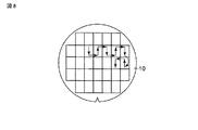
図8は、各露光フィールドを順次走査露光する際の露光順序の一例を表す半導体基板10の平面図である。図8における上向きの矢印・下向きの矢印はそれぞれ、露光スリット領域が移動する方向を示している。図8に示すように、一つの露光フィールドをスキャン露光し、隣の露光フィールドをスキャン露光するときには、走査の向きが逆になっている。このような動作を繰り返しながら半導体基板10全面の露光を行う。
FIG. 8 is a plan view of the
ところで、スキャン露光の間、水供給・排出器36,36はフェンス35で囲まれた領域の外に超純水が残らないように超純水の回収を行う。ところが、半導体基板上の保護膜が超純水をはじきやすい(保護膜の超純水に対する接触角が大きい)場合や、ステージ34の移動速度が速い場合や、ステージ34の加減速度が大きい場合や、比較的大きい露光領域を有する場合などでは、図9に示すように、半導体基板10の保護膜上に残留水71が生じてしまう。保護膜上に残留水71があると、超純水が保護膜の表面に吸着したり、超純水が保護膜中に浸入して保護膜中に吸収されたりする。
By the way, during the scanning exposure, the water supply /
この超純水が保護膜に吸着または吸収された状態で、次の加熱(Post exposure bake)を行うと、超純水が吸着または吸収された部分では、熱が吸収されて他の部分と比べてレジスト膜へ供給される熱量が少なくなり、レジスト膜中での加熱による反応を十分に生じさせることができず線幅異常が生じる。レジストがポジレジストである場合には未開口の欠陥が発生してしまう。ネガレジストである場合にはオープン不良の欠陥が発生するという問題が生じる。 When the next heating (post exposure bake) is performed in a state where the ultrapure water is adsorbed or absorbed by the protective film, heat is absorbed in the portion where the ultrapure water is adsorbed or absorbed, compared with other portions. As a result, the amount of heat supplied to the resist film is reduced, and a reaction caused by heating in the resist film cannot be sufficiently caused, resulting in an abnormal line width. If the resist is a positive resist, an unopened defect occurs. In the case of a negative resist, there arises a problem that an open defect occurs.
これらの問題を解消するため、露光装置から搬出された半導体基板に対して、保護膜上に残った残留水及び保護膜に吸収された純水を除去する必要がある。本第1の実施の形態では、疎水性の第1の保護膜52の表面に親水性の第2の保護膜53が設けられているので、第2の保護膜53上では水分は凝集しにくく、water−markが生じにくくなる。
In order to solve these problems, it is necessary to remove residual water remaining on the protective film and pure water absorbed by the protective film from the semiconductor substrate carried out of the exposure apparatus. In the first embodiment, since the hydrophilic second
なお、第1の保護膜52における超純水のトラップ能力が不十分で、液浸露光時に超純水がレジスト膜51に浸入していれば、保護膜53上及び保護膜52,53中の超純水の除去と共にレジスト膜51に浸入した超純水の除去を行う。しかし、第1の保護膜52の超純水のトラップ能力が十分で、レジスト膜51に超純水が浸入していなければ、レジスト膜51からの超純水の除去は行わない。
If the ultra-pure water trapping capability of the first
次に、レジスト膜51表面の第2の保護膜53を除去し(ステップST108)、第1の保護膜52を除去する(ステップST109)。これらの処理を行った半導体基板10をベーカーに搬送して、半導体基板10の加熱(PEB)を行う(ステップST110)。この加熱により、露光段階で発生した酸の拡散、増幅反応を行う。さらに、半導体基板10を現像ユニットに搬送し現像を行い、ArFレジストパターンが形成される(ステップST111)。
Next, the second
あるいは露光の後に、PEBを行い(ステップST110)、第2の保護膜53を除去し(ステップST108)、第1の保護膜52を除去する(ステップST109)こともできる。あるいは露光の後に、第2の保護膜53を除去し(ステップST108)、PEBを行い(ステップST110)、第1の保護膜52を除去する(ステップST109)こともできる。これらの処理の後、現像処理を行う(ステップST111)。以上のように形成されたレジストパターンを有する半導体基板を用いて半導体装置を製造することができる。
Alternatively, PEB may be performed after exposure (step ST110), the second
なお、反射防止膜が必要とされない場合には、上記ステップST101を省略しても良い。 If an antireflection film is not required, step ST101 may be omitted.
なお、保護膜52,53が現像液に可溶である場合には、現像時に保護膜52,53を除去しても良い。また、ArF化学増幅型レジスト膜の表面に酸発生材や酸トラップ材(アミンなど)が存在しない場合には、上記ステップST103,ST104は省略してもよい。
When the
また、上記の製造工程では超純水との接触角が110°程度である第1の保護膜52を形成したが、第2の保護膜を第1の保護膜と独立して形成する場合には、超純水との接触角が75°程度である第1の保護膜52を形成し、基板を80℃程度に保ちながら第1の保護膜52の表面を有機シラザン化合物、具体的にはヘキサメチルジシラザンまたはトリメチルジシラザンの雰囲気にさらして、第1の保護膜52の表面を改質し疎水化処理を行ってもよい。この場合、第1の保護膜52と超純水との接触角が80°以上となる層(高接触角層)が形成されるように改質することが好ましい。なお、超純水との接触角が75°程度である第1の保護膜52の表面を有機シラザン化合物またはフッ素化合物の液体もしくは雰囲気に暴露させて、第1の保護膜52の表面を改質してもよい。
In the manufacturing process described above, the first
ところで、少なくとも露光装置から露光後の水処理ユニットを経てベーカーに至るまでの工程では、雰囲気制御を行う必要がある。レジストパターン形成に影響を与えない程度に酸の失活を抑えるには、塩基性物質の濃度を10ppb以下にする必要があることが判った。また、搬送時間を含む処理時間についても±10%の範囲で管理することが望ましいという実験結果を得た。 By the way, it is necessary to control the atmosphere at least from the exposure apparatus through the post-exposure water treatment unit to the baker. It was found that the concentration of the basic substance needs to be 10 ppb or less in order to suppress the deactivation of the acid to the extent that it does not affect the formation of the resist pattern. Moreover, the experimental result that it was desirable to manage also about the processing time including conveyance time in the range of +/- 10% was obtained.
図10の(a)(b)は、従来例に係るレジスト膜(水に対する接触角が75°)上の保護膜を示す図である。図10の(a)に示すように第1の保護膜(液浸液に対して親和性の低い膜:水に対する接触角が90°以上)52のみを用いた場合、保護膜上の液滴54が小さくなり内圧が大きくなると、保護膜の液浸液に対して比較的親和性の高い部分から液が染み込み、図10の(b)に示すように第1の保護膜52とレジスト膜51表面との界面で広がる。広がった液膜の圧力は小さくなるため、保護膜52を透過して外に出ることができず、この部分に留まるか、その下のレジスト膜51に浸透し、最終的にwater−mark55を形成してしまう。
FIGS. 10A and 10B are diagrams showing a protective film on a resist film (contact angle with respect to water of 75 °) according to a conventional example. As shown in FIG. 10A, when only the first protective film 52 (film having a low affinity for the immersion liquid: the contact angle with respect to water is 90 ° or more) 52 is used, a droplet on the protective film is used. When 54 becomes smaller and the internal pressure becomes larger, the liquid soaks in from a portion having a relatively high affinity for the immersion liquid in the protective film, and the first
図11の(a)(b)は、別の従来例に係るレジスト膜(水に対する接触角が75°)上の保護膜を示す図である。図11の(a)に示すように第2の保護膜(液浸液に対して親和性の高い膜:水に対する接触角が90°未満)53のみを用いた場合、保護膜上の液嫡4が容易に浸透して、図11の(b)に示すように第2の保護膜53とレジスト膜51表面との界面に達する。界面に達した水は、界面で広がるかその下のレジスト膜51に浸透し、この場合も最終的にwater−mark55を形成してしまう。
FIGS. 11A and 11B are diagrams showing a protective film on a resist film (contact angle with respect to water of 75 °) according to another conventional example. As shown in FIG. 11 (a), when only the second protective film 53 (film having high affinity for immersion liquid: contact angle with water is less than 90 °) 53 is used, the liquid on the
図12の(a)(b)は、本実施の形態に係るレジスト膜(水に対する接触角が75°)上の保護膜を示す図である。本実施の形態において、図12の(a)に示すように液浸液に対して親和性の低い(水に対する接触角が90°以上)第1の保護膜52の表面に第1の保護膜52よりも液浸液に対して親和性の高い(水に対する接触角が90°未満)第2の保護膜53を形成したのは、以下の理由による。
FIGS. 12A and 12B are views showing a protective film on the resist film (contact angle with water is 75 °) according to the present embodiment. In the present embodiment, as shown in FIG. 12A, the first protective film on the surface of the first
図12の(a)に示すように、第2の保護膜53上に形成された液滴54は親和性の高い第2の保護膜53に浸透するが、浸透性が高いために拡散する。液滴54が親和性の低い第1の保護膜52に到達した際には、液が広がりを持っているため圧力は小さくなる。このため、浸透した液滴54は第1の保護膜52を透過する力がなく、図12の(b)に示すように第1の保護膜52と第2の保護膜53の間に保持され、レジスト膜51上には到達しない。従って、レジストの性能をなんら損失することはなく、また、レジスト膜51上にwater−markは形成されない。なお、第1の保護膜52は液浸液に対してできるだけ親和性を低くすると良い。
As shown in FIG. 12A, the
この機能を最大限に生かすには、液浸液に対して親和性の高い第2の保護膜53上に親和性の低い第3の保護膜を形成すると良く、かつ第3の保護膜を液浸液に対してできるだけ親和性を低くし、第2の保護膜53を液浸液に対してできるだけ親和性を高くすると良い。
In order to make the most of this function, a third protective film having a low affinity should be formed on the second
なお、第2の保護膜53には親水化処理を行ってもよい。この処理は、第2の保護膜53上にオゾンの濃度が20ppm程度のオゾン水を30秒程度供給することによって行われる。オゾン水によって第2の保護膜53の表面が除去されると同時に表面と超純水との接触角が5°以下になった。本第1の実施の形態では、図5(c)に示すように、親水層(低接触角層)である第2の保護膜53と超純水との接触角が5゜になり、レジスト膜51と超純水との接触角(75゜)よりも小さくなっている。なお、第2の保護膜53の親水化には、表面にオゾンを含む液体を暴露させる代わりに、オゾンを含む気体を暴露させてもよい。
Note that the second
本実施の形態によれば、レジストよりも疎水性の高い保護膜をレジスト膜に形成し、その保護膜上に液浸露光を行うことで、液浸露光時のレジスト膜への超純水の浸入を抑えることができる。また、レジスト組成物から液浸溶液への汚染を抑制することができる。さらに、保護膜表面を親水化しており、液浸露光後に超純水の除去を行うことによって、water−markを生じることなく保護膜表面の残留水を除去することができる。その結果、パターン形成不良の発生を抑制することができる。 According to the present embodiment, a protective film having a hydrophobicity higher than that of the resist is formed on the resist film, and immersion exposure is performed on the protective film, so that ultrapure water is applied to the resist film during the immersion exposure. Infiltration can be suppressed. Further, contamination from the resist composition to the immersion solution can be suppressed. Furthermore, the surface of the protective film is hydrophilized, and by removing ultrapure water after immersion exposure, residual water on the surface of the protective film can be removed without causing water-mark. As a result, occurrence of pattern formation defects can be suppressed.
なお本実施の形態では、露光の際にレンズと被処理基板(半導体基板)との間に介在させた液浸溶液には、脱気させた超純水を用いていたが、これに限るものではない。屈折率を大きくするためにI族、II族などのアルカリイオンを添加したり、吸収係数を小さくするために酸イオンを添加した液体を用いたりしてもよい。露光光に対して吸収係数が小さく、特定の屈折率に併せた露光装置を用いる場合、特定の屈折率を有する液体であって、レンズ系などにダメージを与えないものであればいかなるものを用いてもよい。 In this embodiment, degassed ultrapure water is used as the immersion solution interposed between the lens and the substrate to be processed (semiconductor substrate) in the exposure. However, the present invention is not limited to this. is not. Alkali ions such as Group I and Group II may be added to increase the refractive index, or a liquid added with acid ions may be used to decrease the absorption coefficient. When using an exposure apparatus that has a small absorption coefficient for exposure light and that has a specific refractive index, any liquid that has a specific refractive index and that does not damage the lens system or the like is used. May be.
また本実施の形態は、ArF(193nm)光を用いた露光に関するが、KrF(248nm)光を用いた露光に関しても、同様の処理を行うことで精度良くパターニングを行うことができる。またF2(157nm)露光では、第1の溶媒にフッ素系オイルを用いることで精度良くパターニングを行うことができることを確認した。 Further, although this embodiment relates to exposure using ArF (193 nm) light, patterning can be performed with high accuracy by performing the same processing for exposure using KrF (248 nm) light. In F 2 (157 nm) exposure, it was confirmed that patterning can be performed with high accuracy by using a fluorinated oil as the first solvent.
また本実施の形態では、液浸液、第1の保護膜52、第2の保護膜53として、”Characterization of refractive properties of fluids for immersion photolithography”, Simon G. Kaplan, John H. Burnett, Xiaoping Gao and Peng Zhang,
International Symposium on Immersion and 157 nm Lithography 8-3-2004に開示されているものを使用できる。
In the present embodiment, the immersion liquid, the first
Those disclosed in International Symposium on Immersion and 157 nm Lithography 8-3-2004 can be used.
有機系液浸液として、アルコール系溶剤であるイソプロパノール、グリセロール、石油系溶剤であるn-ヘキサン、n-ヘプタン、n-デカンを使用できる。 As the organic immersion liquid, alcoholic solvents such as isopropanol and glycerol, and petroleum solvents n-hexane, n-heptane, and n-decane can be used.
アルコール系溶剤を使用する場合、水の場合と同様に、第1の保護膜52として疎水性ポリマーやフッ素系樹脂を使用し、第2の保護膜53としてポリシクロペンテンを使用する。親水化処理としてオゾン水処理を行う。
When an alcohol solvent is used, a hydrophobic polymer or a fluorine resin is used as the first
石油系溶剤を使用する場合、第1の保護膜として疎油性ポリマーを使用し、溶剤にイソプロパノール、イソブタノール等のアルコール系溶剤を使用する。第1の保護膜の樹脂の代表例として、ポリ酢酸ビニルの部分加水分解物、ポリビニルアルコール、ポリエチレングリコールが挙げられる。第2の保護膜として親油性ポリマーを使用し、溶剤にシクロヘキサノン、メチルイソブチルケトン等のケトン系溶剤を使用する。第2の保護膜の樹脂の代表例として、アクリル酸アダマンチル・スチレン共重合体、水添ポリイソブテンが挙げられる。 When a petroleum solvent is used, an oleophobic polymer is used as the first protective film, and an alcohol solvent such as isopropanol or isobutanol is used as the solvent. Typical examples of the resin for the first protective film include polyvinyl acetate partial hydrolyzate, polyvinyl alcohol, and polyethylene glycol. A lipophilic polymer is used as the second protective film, and a ketone solvent such as cyclohexanone or methyl isobutyl ketone is used as the solvent. Typical examples of the resin for the second protective film include adamantyl acrylate / styrene copolymer and hydrogenated polyisobutene.
なお、本発明は上記実施の形態のみに限定されず、要旨を変更しない範囲で適宜変形して実施できる。 In addition, this invention is not limited only to the said embodiment, In the range which does not change a summary, it can deform | transform suitably and can be implemented.
10…半導体基板(半導体ウェハ) 31…レチクルステージ 32…レチクル 33…投影レンズ系 34…ウェハステージ 35…フェンス 36…水供給・排出器 37…サポート板 21…エアーナイフ 22…ガス 51…レジスト膜 52…第1の保護膜 53…第2の保護膜 54…液滴 55…water−mark 61…膜 62…超純水
DESCRIPTION OF
Claims (11)
被処理基板上にレジスト膜を形成する工程であり、前記レジスト膜と液浸溶液との接触角が第1の角度である工程と、
前記レジスト膜上に第1の保護膜を形成する工程であり、前記第1の保護膜と前記液浸溶液との接触角が前記第1の角度よりも大きい第2の角度である工程と、
前記第1の保護膜上に第2の保護膜を形成する工程であり、前記2の保護膜と前記液浸溶液との接触角が前記第2の角度よりも小さい第3の角度である工程と、
液浸露光により前記レジスト膜に潜像を形成する工程と、
を有することを特徴とするレジストパターン形成方法。 A resist pattern forming method for forming a resist pattern by immersion exposure,
A step of forming a resist film on the substrate to be processed, wherein the contact angle between the resist film and the immersion solution is a first angle;
Forming a first protective film on the resist film, wherein a contact angle between the first protective film and the immersion solution is a second angle larger than the first angle;
Forming a second protective film on the first protective film, wherein the contact angle between the second protective film and the immersion solution is a third angle smaller than the second angle; When,
Forming a latent image on the resist film by immersion exposure; and
A resist pattern forming method characterized by comprising:
Priority Applications (4)
| Application Number | Priority Date | Filing Date | Title |
|---|---|---|---|
| JP2004378298A JP4488890B2 (en) | 2004-12-27 | 2004-12-27 | Resist pattern forming method and semiconductor device manufacturing method |
| TW094143749A TWI286341B (en) | 2004-12-27 | 2005-12-09 | Method for forming resist pattern and method for manufacturing semiconductor device |
| KR1020050129528A KR100770821B1 (en) | 2004-12-27 | 2005-12-26 | Method of Forming a Resist Pattern and Method of Manufacturing of a Semiconductor Device |
| US11/316,898 US7687227B2 (en) | 2004-12-27 | 2005-12-27 | Resist pattern forming method and manufacturing method of semiconductor device |
Applications Claiming Priority (1)
| Application Number | Priority Date | Filing Date | Title |
|---|---|---|---|
| JP2004378298A JP4488890B2 (en) | 2004-12-27 | 2004-12-27 | Resist pattern forming method and semiconductor device manufacturing method |
Publications (2)
| Publication Number | Publication Date |
|---|---|
| JP2006186111A true JP2006186111A (en) | 2006-07-13 |
| JP4488890B2 JP4488890B2 (en) | 2010-06-23 |
Family
ID=36739006
Family Applications (1)
| Application Number | Title | Priority Date | Filing Date |
|---|---|---|---|
| JP2004378298A Expired - Fee Related JP4488890B2 (en) | 2004-12-27 | 2004-12-27 | Resist pattern forming method and semiconductor device manufacturing method |
Country Status (4)
| Country | Link |
|---|---|
| US (1) | US7687227B2 (en) |
| JP (1) | JP4488890B2 (en) |
| KR (1) | KR100770821B1 (en) |
| TW (1) | TWI286341B (en) |
Cited By (12)
| Publication number | Priority date | Publication date | Assignee | Title |
|---|---|---|---|---|
| JP2006189687A (en) * | 2005-01-07 | 2006-07-20 | Jsr Corp | Method for forming photoresist pattern, and substrate for forming the photoresist pattern |
| WO2006115186A1 (en) * | 2005-04-25 | 2006-11-02 | Nikon Corporation | Exposure method, exposure apparatus and device manufacturing method |
| JP2007005660A (en) * | 2005-06-24 | 2007-01-11 | Dainippon Screen Mfg Co Ltd | Substrate processor |
| JP2008139831A (en) * | 2006-12-01 | 2008-06-19 | Hynix Semiconductor Inc | Method for forming fine pattern of semiconductor device |
| JP2008203638A (en) * | 2007-02-21 | 2008-09-04 | Tokyo Electron Ltd | Method for treating substrate and pre-wet solvent for overlay film agent to be applied on surface of resist film |
| EP1918778A3 (en) * | 2006-10-30 | 2009-04-29 | Rohm and Haas Electronic Materials LLC | Compositions and processes for immersion lithography |
| US7556914B2 (en) | 2005-01-06 | 2009-07-07 | Panasonic Corporation | Pattern formation method |
| JP2010109148A (en) * | 2008-10-30 | 2010-05-13 | Toshiba Corp | Method of forming resist pattern |
| JP2010211153A (en) * | 2009-03-12 | 2010-09-24 | Renesas Electronics Corp | Resist pattern forming method |
| US8257902B2 (en) | 2007-11-05 | 2012-09-04 | Deyan Wang | Compositons and processes for immersion lithography |
| US8501058B2 (en) | 2008-08-21 | 2013-08-06 | Kabushiki Kaisha Toshiba | Method of cleaning template and pattern forming method |
| US8715902B2 (en) | 2005-05-01 | 2014-05-06 | Rohm And Haas Electronic Materials Llc | Compositions and processes for immersion lithography |
Families Citing this family (6)
| Publication number | Priority date | Publication date | Assignee | Title |
|---|---|---|---|---|
| US20080020324A1 (en) * | 2006-07-19 | 2008-01-24 | Taiwan Semiconductor Manufacturing Company, Ltd. | Immersion lithography defect reduction with top coater removal |
| JP4912180B2 (en) * | 2006-09-15 | 2012-04-11 | 東京エレクトロン株式会社 | Exposure and development processing methods |
| US20080241489A1 (en) * | 2007-03-30 | 2008-10-02 | Renesas Technology Corp. | Method of forming resist pattern and semiconductor device manufactured with the same |
| JP2009117832A (en) * | 2007-11-06 | 2009-05-28 | Asml Netherlands Bv | Method of preparing substrate for lithography, substrate, device manufacturing method, sealing coating applicator, and sealing coating measuring device |
| JP2010027952A (en) * | 2008-07-23 | 2010-02-04 | Toshiba Corp | Method for manufacturing semiconductor device |
| JP7367554B2 (en) * | 2019-03-06 | 2023-10-24 | 信越化学工業株式会社 | Positive resist composition and pattern forming method |
Family Cites Families (19)
| Publication number | Priority date | Publication date | Assignee | Title |
|---|---|---|---|---|
| DK0517996T3 (en) | 1991-06-14 | 1994-04-18 | Procter & Gamble | Stable, hydrogen peroxide-containing bleach compositions |
| JPH08316121A (en) * | 1995-05-17 | 1996-11-29 | Fujitsu Ltd | Resist pattern forming method |
| JP3747566B2 (en) | 1997-04-23 | 2006-02-22 | 株式会社ニコン | Immersion exposure equipment |
| JP3872928B2 (en) * | 2000-03-24 | 2007-01-24 | 株式会社東芝 | Pattern formation method |
| JP3908443B2 (en) * | 2000-06-30 | 2007-04-25 | 株式会社東芝 | Substrate processing method |
| JP4015823B2 (en) * | 2001-05-14 | 2007-11-28 | 株式会社東芝 | Alkali developer manufacturing method, alkali developer, pattern forming method, resist film peeling method, and chemical solution coating apparatus |
| JP4131786B2 (en) * | 2001-09-03 | 2008-08-13 | 株式会社東芝 | Semiconductor device manufacturing method and wafer structure |
| US7018481B2 (en) * | 2002-01-28 | 2006-03-28 | Kabushiki Kaisha Toshiba | Substrate treating method, substrate-processing apparatus, developing method, method of manufacturing a semiconductor device, and method of cleaning a developing solution nozzle |
| US6788477B2 (en) * | 2002-10-22 | 2004-09-07 | Taiwan Semiconductor Manufacturing Co., Ltd. | Apparatus for method for immersion lithography |
| JP2004266008A (en) * | 2003-02-28 | 2004-09-24 | Toshiba Corp | Method for manufacturing semiconductor device |
| JP4054285B2 (en) * | 2003-06-12 | 2008-02-27 | 松下電器産業株式会社 | Pattern formation method |
| EP3104396B1 (en) * | 2003-06-13 | 2018-03-21 | Nikon Corporation | Exposure method, substrate stage, exposure apparatus, and device manufacturing method |
| JP4084712B2 (en) * | 2003-06-23 | 2008-04-30 | 松下電器産業株式会社 | Pattern formation method |
| US7175968B2 (en) * | 2003-07-28 | 2007-02-13 | Asml Netherlands B.V. | Lithographic apparatus, device manufacturing method and a substrate |
| JP3993549B2 (en) * | 2003-09-30 | 2007-10-17 | 株式会社東芝 | Resist pattern forming method |
| US7528929B2 (en) * | 2003-11-14 | 2009-05-05 | Asml Netherlands B.V. | Lithographic apparatus and device manufacturing method |
| TWI222670B (en) | 2003-12-03 | 2004-10-21 | United Microelectronics Corp | Immersion lithography process and mask layer structure applied in the same |
| US20050161644A1 (en) * | 2004-01-23 | 2005-07-28 | Peng Zhang | Immersion lithography fluids |
| JP4521219B2 (en) * | 2004-04-19 | 2010-08-11 | 株式会社東芝 | Drawing pattern generation method, resist pattern formation method, and exposure apparatus control method |
-
2004
- 2004-12-27 JP JP2004378298A patent/JP4488890B2/en not_active Expired - Fee Related
-
2005
- 2005-12-09 TW TW094143749A patent/TWI286341B/en not_active IP Right Cessation
- 2005-12-26 KR KR1020050129528A patent/KR100770821B1/en not_active IP Right Cessation
- 2005-12-27 US US11/316,898 patent/US7687227B2/en not_active Expired - Fee Related
Cited By (25)
| Publication number | Priority date | Publication date | Assignee | Title |
|---|---|---|---|---|
| US7556914B2 (en) | 2005-01-06 | 2009-07-07 | Panasonic Corporation | Pattern formation method |
| JP2006189687A (en) * | 2005-01-07 | 2006-07-20 | Jsr Corp | Method for forming photoresist pattern, and substrate for forming the photoresist pattern |
| JP4696558B2 (en) * | 2005-01-07 | 2011-06-08 | Jsr株式会社 | Photoresist pattern forming method and substrate for forming photoresist pattern |
| JP2010245572A (en) * | 2005-04-25 | 2010-10-28 | Nikon Corp | Exposure method, exposure apparatus, and device manufacturing method |
| WO2006115186A1 (en) * | 2005-04-25 | 2006-11-02 | Nikon Corporation | Exposure method, exposure apparatus and device manufacturing method |
| US8064039B2 (en) | 2005-04-25 | 2011-11-22 | Nikon Corporation | Exposure method, exposure apparatus, and device manufacturing method |
| JP5125505B2 (en) * | 2005-04-25 | 2013-01-23 | 株式会社ニコン | Exposure method, exposure apparatus, and device manufacturing method |
| US9618854B2 (en) | 2005-04-25 | 2017-04-11 | Nikon Corporation | Exposure method, exposure apparatus, and device manufacturing method |
| JPWO2006115186A1 (en) * | 2005-04-25 | 2008-12-18 | 株式会社ニコン | Exposure method, exposure apparatus, and device manufacturing method |
| US9335639B2 (en) | 2005-04-25 | 2016-05-10 | Nikon Corporation | Exposure method, exposure apparatus, and device manufacturing method |
| US9696622B2 (en) | 2005-05-01 | 2017-07-04 | Rohm And Haas Electronic Materials Llc | Compositions and processes for immersion lithography |
| US8715902B2 (en) | 2005-05-01 | 2014-05-06 | Rohm And Haas Electronic Materials Llc | Compositions and processes for immersion lithography |
| JP4514657B2 (en) * | 2005-06-24 | 2010-07-28 | 株式会社Sokudo | Substrate processing equipment |
| JP2007005660A (en) * | 2005-06-24 | 2007-01-11 | Dainippon Screen Mfg Co Ltd | Substrate processor |
| EP1918778A3 (en) * | 2006-10-30 | 2009-04-29 | Rohm and Haas Electronic Materials LLC | Compositions and processes for immersion lithography |
| EP2420891A1 (en) * | 2006-10-30 | 2012-02-22 | Rohm and Haas Electronic Materials LLC | Compositions and processes for immersion lithography |
| EP2420892A1 (en) * | 2006-10-30 | 2012-02-22 | Rohm and Haas Electronic Materials LLC | Compositions and processes for immersion lithography |
| US9244355B2 (en) | 2006-10-30 | 2016-01-26 | Rohm And Haas Electronic Materials, Llc | Compositions and processes for immersion lithography |
| JP2008139831A (en) * | 2006-12-01 | 2008-06-19 | Hynix Semiconductor Inc | Method for forming fine pattern of semiconductor device |
| JP2008203638A (en) * | 2007-02-21 | 2008-09-04 | Tokyo Electron Ltd | Method for treating substrate and pre-wet solvent for overlay film agent to be applied on surface of resist film |
| US8257902B2 (en) | 2007-11-05 | 2012-09-04 | Deyan Wang | Compositons and processes for immersion lithography |
| US8871428B2 (en) | 2007-11-05 | 2014-10-28 | Rohm And Haas Electronics Materials Llc | Compositions and processes for immersion lithography |
| US8501058B2 (en) | 2008-08-21 | 2013-08-06 | Kabushiki Kaisha Toshiba | Method of cleaning template and pattern forming method |
| JP2010109148A (en) * | 2008-10-30 | 2010-05-13 | Toshiba Corp | Method of forming resist pattern |
| JP2010211153A (en) * | 2009-03-12 | 2010-09-24 | Renesas Electronics Corp | Resist pattern forming method |
Also Published As
| Publication number | Publication date |
|---|---|
| US20070042297A1 (en) | 2007-02-22 |
| KR20060074860A (en) | 2006-07-03 |
| TW200701300A (en) | 2007-01-01 |
| KR100770821B1 (en) | 2007-10-26 |
| JP4488890B2 (en) | 2010-06-23 |
| TWI286341B (en) | 2007-09-01 |
| US7687227B2 (en) | 2010-03-30 |
Similar Documents
| Publication | Publication Date | Title |
|---|---|---|
| KR100770821B1 (en) | Method of Forming a Resist Pattern and Method of Manufacturing of a Semiconductor Device | |
| KR100814040B1 (en) | Immersion lithography defect reduction | |
| JP4220423B2 (en) | Resist pattern forming method | |
| US8383322B2 (en) | Immersion lithography watermark reduction | |
| US20060008746A1 (en) | Method for manufacturing semiconductor device | |
| KR100801161B1 (en) | Methods and system for inhibiting immersion lithography defect formation | |
| JP2006024692A (en) | Forming method of resist pattern | |
| JP2010182732A (en) | Method of manufacturing semiconductor device | |
| JP4167642B2 (en) | Resist pattern forming method | |
| JP2012256726A (en) | Rework method for resist film, manufacturing method for semiconductor device, and substrate processing system | |
| JP4718893B2 (en) | Pattern formation method | |
| TWI401542B (en) | Immersion lithography defect reduction with top coater removal | |
| US5356758A (en) | Method and apparatus for positively patterning a surface-sensitive resist on a semiconductor wafer | |
| JP4374042B2 (en) | Manufacturing method of semiconductor device | |
| Streefkerk et al. | A dive into clear water: immersion defect capabilities | |
| US6555234B1 (en) | Barrier for and a method of reducing outgassing from a photoresist material | |
| JP4672763B2 (en) | Resist pattern forming method | |
| US7998663B2 (en) | Pattern formation method | |
| JP2007088256A (en) | Pattern forming method and manufacturing method of semiconductor device | |
| US6291135B1 (en) | Ionization technique to reduce defects on next generation lithography mask during exposure | |
| JP2005250084A (en) | Pattern forming method | |
| KR20070017061A (en) | Immersion lithography watermark reduction |
Legal Events
| Date | Code | Title | Description |
|---|---|---|---|
| A621 | Written request for application examination |
Free format text: JAPANESE INTERMEDIATE CODE: A621 Effective date: 20070904 |
|
| A977 | Report on retrieval |
Free format text: JAPANESE INTERMEDIATE CODE: A971007 Effective date: 20100225 |
|
| TRDD | Decision of grant or rejection written | ||
| A01 | Written decision to grant a patent or to grant a registration (utility model) |
Free format text: JAPANESE INTERMEDIATE CODE: A01 Effective date: 20100302 |
|
| A01 | Written decision to grant a patent or to grant a registration (utility model) |
Free format text: JAPANESE INTERMEDIATE CODE: A01 |
|
| A61 | First payment of annual fees (during grant procedure) |
Free format text: JAPANESE INTERMEDIATE CODE: A61 Effective date: 20100330 |
|
| FPAY | Renewal fee payment (event date is renewal date of database) |
Free format text: PAYMENT UNTIL: 20130409 Year of fee payment: 3 |
|
| FPAY | Renewal fee payment (event date is renewal date of database) |
Free format text: PAYMENT UNTIL: 20130409 Year of fee payment: 3 |
|
| LAPS | Cancellation because of no payment of annual fees |