JP2006134912A - Semiconductor module and its manufacturing method, and film interposer - Google Patents
Semiconductor module and its manufacturing method, and film interposer Download PDFInfo
- Publication number
- JP2006134912A JP2006134912A JP2004318891A JP2004318891A JP2006134912A JP 2006134912 A JP2006134912 A JP 2006134912A JP 2004318891 A JP2004318891 A JP 2004318891A JP 2004318891 A JP2004318891 A JP 2004318891A JP 2006134912 A JP2006134912 A JP 2006134912A
- Authority
- JP
- Japan
- Prior art keywords
- semiconductor
- insulating resin
- resin layer
- semiconductor module
- semiconductor element
- Prior art date
- Legal status (The legal status is an assumption and is not a legal conclusion. Google has not performed a legal analysis and makes no representation as to the accuracy of the status listed.)
- Withdrawn
Links
- 239000004065 semiconductor Substances 0.000 title claims abstract description 390
- 238000004519 manufacturing process Methods 0.000 title claims description 39
- 239000011347 resin Substances 0.000 claims abstract description 118
- 229920005989 resin Polymers 0.000 claims abstract description 118
- 238000000034 method Methods 0.000 claims description 128
- 229910052751 metal Inorganic materials 0.000 claims description 17
- 239000002184 metal Substances 0.000 claims description 17
- 229910000679 solder Inorganic materials 0.000 claims description 16
- 239000004760 aramid Substances 0.000 claims description 13
- 229920003235 aromatic polyamide Polymers 0.000 claims description 13
- 230000000149 penetrating effect Effects 0.000 claims description 13
- 229920001721 polyimide Polymers 0.000 claims description 13
- 239000004642 Polyimide Substances 0.000 claims description 8
- PCHJSUWPFVWCPO-UHFFFAOYSA-N gold Chemical compound [Au] PCHJSUWPFVWCPO-UHFFFAOYSA-N 0.000 claims description 8
- 238000003825 pressing Methods 0.000 claims description 8
- 239000011248 coating agent Substances 0.000 claims description 7
- 238000000576 coating method Methods 0.000 claims description 7
- 229910052782 aluminium Inorganic materials 0.000 claims description 6
- 229910052737 gold Inorganic materials 0.000 claims description 6
- 239000010931 gold Substances 0.000 claims description 6
- 238000005304 joining Methods 0.000 claims description 6
- BASFCYQUMIYNBI-UHFFFAOYSA-N platinum Chemical compound [Pt] BASFCYQUMIYNBI-UHFFFAOYSA-N 0.000 claims description 6
- XAGFODPZIPBFFR-UHFFFAOYSA-N aluminium Chemical compound [Al] XAGFODPZIPBFFR-UHFFFAOYSA-N 0.000 claims description 5
- 150000002739 metals Chemical class 0.000 claims description 5
- 230000000007 visual effect Effects 0.000 claims description 4
- BQCADISMDOOEFD-UHFFFAOYSA-N Silver Chemical compound [Ag] BQCADISMDOOEFD-UHFFFAOYSA-N 0.000 claims description 3
- 229910045601 alloy Inorganic materials 0.000 claims description 3
- 239000000956 alloy Substances 0.000 claims description 3
- 229910052697 platinum Inorganic materials 0.000 claims description 3
- 229910052709 silver Inorganic materials 0.000 claims description 3
- 239000004332 silver Substances 0.000 claims description 3
- 229910052720 vanadium Inorganic materials 0.000 claims description 3
- LEONUFNNVUYDNQ-UHFFFAOYSA-N vanadium atom Chemical compound [V] LEONUFNNVUYDNQ-UHFFFAOYSA-N 0.000 claims description 3
- 238000005516 engineering process Methods 0.000 abstract description 5
- 239000010408 film Substances 0.000 description 203
- 239000010410 layer Substances 0.000 description 82
- 239000000758 substrate Substances 0.000 description 34
- 239000011229 interlayer Substances 0.000 description 24
- 230000008569 process Effects 0.000 description 20
- RYGMFSIKBFXOCR-UHFFFAOYSA-N Copper Chemical compound [Cu] RYGMFSIKBFXOCR-UHFFFAOYSA-N 0.000 description 15
- 238000007789 sealing Methods 0.000 description 11
- 229910052802 copper Inorganic materials 0.000 description 10
- 239000010949 copper Substances 0.000 description 10
- OAICVXFJPJFONN-UHFFFAOYSA-N Phosphorus Chemical compound [P] OAICVXFJPJFONN-UHFFFAOYSA-N 0.000 description 8
- 239000012790 adhesive layer Substances 0.000 description 6
- 230000008901 benefit Effects 0.000 description 6
- 238000012546 transfer Methods 0.000 description 6
- 238000003466 welding Methods 0.000 description 6
- 230000015572 biosynthetic process Effects 0.000 description 5
- 239000011889 copper foil Substances 0.000 description 5
- 230000006870 function Effects 0.000 description 5
- 239000000463 material Substances 0.000 description 5
- 238000012986 modification Methods 0.000 description 5
- 230000004048 modification Effects 0.000 description 5
- 238000012790 confirmation Methods 0.000 description 4
- 239000004020 conductor Substances 0.000 description 3
- 238000002844 melting Methods 0.000 description 3
- 230000008018 melting Effects 0.000 description 3
- -1 polypropylene Polymers 0.000 description 3
- 238000001039 wet etching Methods 0.000 description 3
- 239000004593 Epoxy Substances 0.000 description 2
- 239000004734 Polyphenylene sulfide Substances 0.000 description 2
- 239000003795 chemical substances by application Substances 0.000 description 2
- 230000017525 heat dissipation Effects 0.000 description 2
- 239000011159 matrix material Substances 0.000 description 2
- 230000002093 peripheral effect Effects 0.000 description 2
- 229920003207 poly(ethylene-2,6-naphthalate) Polymers 0.000 description 2
- 239000011112 polyethylene naphthalate Substances 0.000 description 2
- 229920000139 polyethylene terephthalate Polymers 0.000 description 2
- 239000005020 polyethylene terephthalate Substances 0.000 description 2
- 229920000069 polyphenylene sulfide Polymers 0.000 description 2
- JMASRVWKEDWRBT-UHFFFAOYSA-N Gallium nitride Chemical compound [Ga]#N JMASRVWKEDWRBT-UHFFFAOYSA-N 0.000 description 1
- 239000004743 Polypropylene Substances 0.000 description 1
- 239000004820 Pressure-sensitive adhesive Substances 0.000 description 1
- 238000010521 absorption reaction Methods 0.000 description 1
- 239000000853 adhesive Substances 0.000 description 1
- 230000001070 adhesive effect Effects 0.000 description 1
- 230000008859 change Effects 0.000 description 1
- 238000007796 conventional method Methods 0.000 description 1
- 230000000994 depressogenic effect Effects 0.000 description 1
- 238000009792 diffusion process Methods 0.000 description 1
- 238000007772 electroless plating Methods 0.000 description 1
- 238000005530 etching Methods 0.000 description 1
- 230000005284 excitation Effects 0.000 description 1
- 230000000704 physical effect Effects 0.000 description 1
- 229920003229 poly(methyl methacrylate) Polymers 0.000 description 1
- 229920001690 polydopamine Polymers 0.000 description 1
- 239000004926 polymethyl methacrylate Substances 0.000 description 1
- 229920001155 polypropylene Polymers 0.000 description 1
- 238000012545 processing Methods 0.000 description 1
- 238000009751 slip forming Methods 0.000 description 1
- 239000007790 solid phase Substances 0.000 description 1
- 239000010409 thin film Substances 0.000 description 1
- 238000013518 transcription Methods 0.000 description 1
- 230000035897 transcription Effects 0.000 description 1
Images


Classifications
-
- H—ELECTRICITY
- H01—ELECTRIC ELEMENTS
- H01L—SEMICONDUCTOR DEVICES NOT COVERED BY CLASS H10
- H01L21/00—Processes or apparatus adapted for the manufacture or treatment of semiconductor or solid state devices or of parts thereof
- H01L21/02—Manufacture or treatment of semiconductor devices or of parts thereof
- H01L21/04—Manufacture or treatment of semiconductor devices or of parts thereof the devices having potential barriers, e.g. a PN junction, depletion layer or carrier concentration layer
- H01L21/48—Manufacture or treatment of parts, e.g. containers, prior to assembly of the devices, using processes not provided for in a single one of the subgroups H01L21/06 - H01L21/326
- H01L21/4814—Conductive parts
- H01L21/4846—Leads on or in insulating or insulated substrates, e.g. metallisation
- H01L21/486—Via connections through the substrate with or without pins
-
- H—ELECTRICITY
- H01—ELECTRIC ELEMENTS
- H01L—SEMICONDUCTOR DEVICES NOT COVERED BY CLASS H10
- H01L23/00—Details of semiconductor or other solid state devices
- H01L23/48—Arrangements for conducting electric current to or from the solid state body in operation, e.g. leads, terminal arrangements ; Selection of materials therefor
- H01L23/488—Arrangements for conducting electric current to or from the solid state body in operation, e.g. leads, terminal arrangements ; Selection of materials therefor consisting of soldered or bonded constructions
- H01L23/498—Leads, i.e. metallisations or lead-frames on insulating substrates, e.g. chip carriers
- H01L23/49827—Via connections through the substrates, e.g. pins going through the substrate, coaxial cables
-
- H—ELECTRICITY
- H01—ELECTRIC ELEMENTS
- H01L—SEMICONDUCTOR DEVICES NOT COVERED BY CLASS H10
- H01L23/00—Details of semiconductor or other solid state devices
- H01L23/48—Arrangements for conducting electric current to or from the solid state body in operation, e.g. leads, terminal arrangements ; Selection of materials therefor
- H01L23/488—Arrangements for conducting electric current to or from the solid state body in operation, e.g. leads, terminal arrangements ; Selection of materials therefor consisting of soldered or bonded constructions
- H01L23/498—Leads, i.e. metallisations or lead-frames on insulating substrates, e.g. chip carriers
- H01L23/4985—Flexible insulating substrates
-
- H—ELECTRICITY
- H01—ELECTRIC ELEMENTS
- H01L—SEMICONDUCTOR DEVICES NOT COVERED BY CLASS H10
- H01L23/00—Details of semiconductor or other solid state devices
- H01L23/52—Arrangements for conducting electric current within the device in operation from one component to another, i.e. interconnections, e.g. wires, lead frames
- H01L23/538—Arrangements for conducting electric current within the device in operation from one component to another, i.e. interconnections, e.g. wires, lead frames the interconnection structure between a plurality of semiconductor chips being formed on, or in, insulating substrates
- H01L23/5389—Arrangements for conducting electric current within the device in operation from one component to another, i.e. interconnections, e.g. wires, lead frames the interconnection structure between a plurality of semiconductor chips being formed on, or in, insulating substrates the chips being integrally enclosed by the interconnect and support structures
-
- H—ELECTRICITY
- H01—ELECTRIC ELEMENTS
- H01L—SEMICONDUCTOR DEVICES NOT COVERED BY CLASS H10
- H01L24/00—Arrangements for connecting or disconnecting semiconductor or solid-state bodies; Methods or apparatus related thereto
- H01L24/01—Means for bonding being attached to, or being formed on, the surface to be connected, e.g. chip-to-package, die-attach, "first-level" interconnects; Manufacturing methods related thereto
- H01L24/18—High density interconnect [HDI] connectors; Manufacturing methods related thereto
- H01L24/19—Manufacturing methods of high density interconnect preforms
-
- H—ELECTRICITY
- H01—ELECTRIC ELEMENTS
- H01L—SEMICONDUCTOR DEVICES NOT COVERED BY CLASS H10
- H01L2224/00—Indexing scheme for arrangements for connecting or disconnecting semiconductor or solid-state bodies and methods related thereto as covered by H01L24/00
- H01L2224/01—Means for bonding being attached to, or being formed on, the surface to be connected, e.g. chip-to-package, die-attach, "first-level" interconnects; Manufacturing methods related thereto
- H01L2224/02—Bonding areas; Manufacturing methods related thereto
- H01L2224/03—Manufacturing methods
- H01L2224/034—Manufacturing methods by blanket deposition of the material of the bonding area
- H01L2224/0343—Manufacturing methods by blanket deposition of the material of the bonding area in solid form
- H01L2224/03436—Lamination of a preform, e.g. foil, sheet or layer
- H01L2224/03438—Lamination of a preform, e.g. foil, sheet or layer the preform being at least partly pre-patterned
-
- H—ELECTRICITY
- H01—ELECTRIC ELEMENTS
- H01L—SEMICONDUCTOR DEVICES NOT COVERED BY CLASS H10
- H01L2224/00—Indexing scheme for arrangements for connecting or disconnecting semiconductor or solid-state bodies and methods related thereto as covered by H01L24/00
- H01L2224/01—Means for bonding being attached to, or being formed on, the surface to be connected, e.g. chip-to-package, die-attach, "first-level" interconnects; Manufacturing methods related thereto
- H01L2224/02—Bonding areas; Manufacturing methods related thereto
- H01L2224/03—Manufacturing methods
- H01L2224/034—Manufacturing methods by blanket deposition of the material of the bonding area
- H01L2224/0343—Manufacturing methods by blanket deposition of the material of the bonding area in solid form
- H01L2224/03436—Lamination of a preform, e.g. foil, sheet or layer
- H01L2224/0344—Lamination of a preform, e.g. foil, sheet or layer by transfer printing
-
- H—ELECTRICITY
- H01—ELECTRIC ELEMENTS
- H01L—SEMICONDUCTOR DEVICES NOT COVERED BY CLASS H10
- H01L2224/00—Indexing scheme for arrangements for connecting or disconnecting semiconductor or solid-state bodies and methods related thereto as covered by H01L24/00
- H01L2224/01—Means for bonding being attached to, or being formed on, the surface to be connected, e.g. chip-to-package, die-attach, "first-level" interconnects; Manufacturing methods related thereto
- H01L2224/02—Bonding areas; Manufacturing methods related thereto
- H01L2224/04—Structure, shape, material or disposition of the bonding areas prior to the connecting process
- H01L2224/05—Structure, shape, material or disposition of the bonding areas prior to the connecting process of an individual bonding area
- H01L2224/05001—Internal layers
- H01L2224/05005—Structure
- H01L2224/05008—Bonding area integrally formed with a redistribution layer on the semiconductor or solid-state body, e.g.
-
- H—ELECTRICITY
- H01—ELECTRIC ELEMENTS
- H01L—SEMICONDUCTOR DEVICES NOT COVERED BY CLASS H10
- H01L2224/00—Indexing scheme for arrangements for connecting or disconnecting semiconductor or solid-state bodies and methods related thereto as covered by H01L24/00
- H01L2224/01—Means for bonding being attached to, or being formed on, the surface to be connected, e.g. chip-to-package, die-attach, "first-level" interconnects; Manufacturing methods related thereto
- H01L2224/02—Bonding areas; Manufacturing methods related thereto
- H01L2224/04—Structure, shape, material or disposition of the bonding areas prior to the connecting process
- H01L2224/05—Structure, shape, material or disposition of the bonding areas prior to the connecting process of an individual bonding area
- H01L2224/05001—Internal layers
- H01L2224/0502—Disposition
- H01L2224/05023—Disposition the whole internal layer protruding from the surface
-
- H—ELECTRICITY
- H01—ELECTRIC ELEMENTS
- H01L—SEMICONDUCTOR DEVICES NOT COVERED BY CLASS H10
- H01L2224/00—Indexing scheme for arrangements for connecting or disconnecting semiconductor or solid-state bodies and methods related thereto as covered by H01L24/00
- H01L2224/01—Means for bonding being attached to, or being formed on, the surface to be connected, e.g. chip-to-package, die-attach, "first-level" interconnects; Manufacturing methods related thereto
- H01L2224/02—Bonding areas; Manufacturing methods related thereto
- H01L2224/04—Structure, shape, material or disposition of the bonding areas prior to the connecting process
- H01L2224/05—Structure, shape, material or disposition of the bonding areas prior to the connecting process of an individual bonding area
- H01L2224/05001—Internal layers
- H01L2224/0502—Disposition
- H01L2224/05026—Disposition the internal layer being disposed in a recess of the surface
- H01L2224/05027—Disposition the internal layer being disposed in a recess of the surface the internal layer extending out of an opening
-
- H—ELECTRICITY
- H01—ELECTRIC ELEMENTS
- H01L—SEMICONDUCTOR DEVICES NOT COVERED BY CLASS H10
- H01L2224/00—Indexing scheme for arrangements for connecting or disconnecting semiconductor or solid-state bodies and methods related thereto as covered by H01L24/00
- H01L2224/01—Means for bonding being attached to, or being formed on, the surface to be connected, e.g. chip-to-package, die-attach, "first-level" interconnects; Manufacturing methods related thereto
- H01L2224/02—Bonding areas; Manufacturing methods related thereto
- H01L2224/04—Structure, shape, material or disposition of the bonding areas prior to the connecting process
- H01L2224/05—Structure, shape, material or disposition of the bonding areas prior to the connecting process of an individual bonding area
- H01L2224/05001—Internal layers
- H01L2224/05099—Material
- H01L2224/051—Material with a principal constituent of the material being a metal or a metalloid, e.g. boron [B], silicon [Si], germanium [Ge], arsenic [As], antimony [Sb], tellurium [Te] and polonium [Po], and alloys thereof
- H01L2224/05117—Material with a principal constituent of the material being a metal or a metalloid, e.g. boron [B], silicon [Si], germanium [Ge], arsenic [As], antimony [Sb], tellurium [Te] and polonium [Po], and alloys thereof the principal constituent melting at a temperature of greater than or equal to 400°C and less than 950°C
- H01L2224/05124—Aluminium [Al] as principal constituent
-
- H—ELECTRICITY
- H01—ELECTRIC ELEMENTS
- H01L—SEMICONDUCTOR DEVICES NOT COVERED BY CLASS H10
- H01L2224/00—Indexing scheme for arrangements for connecting or disconnecting semiconductor or solid-state bodies and methods related thereto as covered by H01L24/00
- H01L2224/01—Means for bonding being attached to, or being formed on, the surface to be connected, e.g. chip-to-package, die-attach, "first-level" interconnects; Manufacturing methods related thereto
- H01L2224/02—Bonding areas; Manufacturing methods related thereto
- H01L2224/04—Structure, shape, material or disposition of the bonding areas prior to the connecting process
- H01L2224/05—Structure, shape, material or disposition of the bonding areas prior to the connecting process of an individual bonding area
- H01L2224/05001—Internal layers
- H01L2224/05099—Material
- H01L2224/051—Material with a principal constituent of the material being a metal or a metalloid, e.g. boron [B], silicon [Si], germanium [Ge], arsenic [As], antimony [Sb], tellurium [Te] and polonium [Po], and alloys thereof
- H01L2224/05138—Material with a principal constituent of the material being a metal or a metalloid, e.g. boron [B], silicon [Si], germanium [Ge], arsenic [As], antimony [Sb], tellurium [Te] and polonium [Po], and alloys thereof the principal constituent melting at a temperature of greater than or equal to 950°C and less than 1550°C
- H01L2224/05139—Silver [Ag] as principal constituent
-
- H—ELECTRICITY
- H01—ELECTRIC ELEMENTS
- H01L—SEMICONDUCTOR DEVICES NOT COVERED BY CLASS H10
- H01L2224/00—Indexing scheme for arrangements for connecting or disconnecting semiconductor or solid-state bodies and methods related thereto as covered by H01L24/00
- H01L2224/01—Means for bonding being attached to, or being formed on, the surface to be connected, e.g. chip-to-package, die-attach, "first-level" interconnects; Manufacturing methods related thereto
- H01L2224/02—Bonding areas; Manufacturing methods related thereto
- H01L2224/04—Structure, shape, material or disposition of the bonding areas prior to the connecting process
- H01L2224/05—Structure, shape, material or disposition of the bonding areas prior to the connecting process of an individual bonding area
- H01L2224/05001—Internal layers
- H01L2224/05099—Material
- H01L2224/051—Material with a principal constituent of the material being a metal or a metalloid, e.g. boron [B], silicon [Si], germanium [Ge], arsenic [As], antimony [Sb], tellurium [Te] and polonium [Po], and alloys thereof
- H01L2224/05138—Material with a principal constituent of the material being a metal or a metalloid, e.g. boron [B], silicon [Si], germanium [Ge], arsenic [As], antimony [Sb], tellurium [Te] and polonium [Po], and alloys thereof the principal constituent melting at a temperature of greater than or equal to 950°C and less than 1550°C
- H01L2224/05144—Gold [Au] as principal constituent
-
- H—ELECTRICITY
- H01—ELECTRIC ELEMENTS
- H01L—SEMICONDUCTOR DEVICES NOT COVERED BY CLASS H10
- H01L2224/00—Indexing scheme for arrangements for connecting or disconnecting semiconductor or solid-state bodies and methods related thereto as covered by H01L24/00
- H01L2224/01—Means for bonding being attached to, or being formed on, the surface to be connected, e.g. chip-to-package, die-attach, "first-level" interconnects; Manufacturing methods related thereto
- H01L2224/02—Bonding areas; Manufacturing methods related thereto
- H01L2224/04—Structure, shape, material or disposition of the bonding areas prior to the connecting process
- H01L2224/05—Structure, shape, material or disposition of the bonding areas prior to the connecting process of an individual bonding area
- H01L2224/05001—Internal layers
- H01L2224/05099—Material
- H01L2224/051—Material with a principal constituent of the material being a metal or a metalloid, e.g. boron [B], silicon [Si], germanium [Ge], arsenic [As], antimony [Sb], tellurium [Te] and polonium [Po], and alloys thereof
- H01L2224/05138—Material with a principal constituent of the material being a metal or a metalloid, e.g. boron [B], silicon [Si], germanium [Ge], arsenic [As], antimony [Sb], tellurium [Te] and polonium [Po], and alloys thereof the principal constituent melting at a temperature of greater than or equal to 950°C and less than 1550°C
- H01L2224/05147—Copper [Cu] as principal constituent
-
- H—ELECTRICITY
- H01—ELECTRIC ELEMENTS
- H01L—SEMICONDUCTOR DEVICES NOT COVERED BY CLASS H10
- H01L2224/00—Indexing scheme for arrangements for connecting or disconnecting semiconductor or solid-state bodies and methods related thereto as covered by H01L24/00
- H01L2224/01—Means for bonding being attached to, or being formed on, the surface to be connected, e.g. chip-to-package, die-attach, "first-level" interconnects; Manufacturing methods related thereto
- H01L2224/02—Bonding areas; Manufacturing methods related thereto
- H01L2224/04—Structure, shape, material or disposition of the bonding areas prior to the connecting process
- H01L2224/05—Structure, shape, material or disposition of the bonding areas prior to the connecting process of an individual bonding area
- H01L2224/05001—Internal layers
- H01L2224/05099—Material
- H01L2224/051—Material with a principal constituent of the material being a metal or a metalloid, e.g. boron [B], silicon [Si], germanium [Ge], arsenic [As], antimony [Sb], tellurium [Te] and polonium [Po], and alloys thereof
- H01L2224/05163—Material with a principal constituent of the material being a metal or a metalloid, e.g. boron [B], silicon [Si], germanium [Ge], arsenic [As], antimony [Sb], tellurium [Te] and polonium [Po], and alloys thereof the principal constituent melting at a temperature of greater than 1550°C
- H01L2224/05169—Platinum [Pt] as principal constituent
-
- H—ELECTRICITY
- H01—ELECTRIC ELEMENTS
- H01L—SEMICONDUCTOR DEVICES NOT COVERED BY CLASS H10
- H01L2224/00—Indexing scheme for arrangements for connecting or disconnecting semiconductor or solid-state bodies and methods related thereto as covered by H01L24/00
- H01L2224/01—Means for bonding being attached to, or being formed on, the surface to be connected, e.g. chip-to-package, die-attach, "first-level" interconnects; Manufacturing methods related thereto
- H01L2224/02—Bonding areas; Manufacturing methods related thereto
- H01L2224/04—Structure, shape, material or disposition of the bonding areas prior to the connecting process
- H01L2224/05—Structure, shape, material or disposition of the bonding areas prior to the connecting process of an individual bonding area
- H01L2224/0554—External layer
- H01L2224/05541—Structure
- H01L2224/05548—Bonding area integrally formed with a redistribution layer on the semiconductor or solid-state body
-
- H—ELECTRICITY
- H01—ELECTRIC ELEMENTS
- H01L—SEMICONDUCTOR DEVICES NOT COVERED BY CLASS H10
- H01L2224/00—Indexing scheme for arrangements for connecting or disconnecting semiconductor or solid-state bodies and methods related thereto as covered by H01L24/00
- H01L2224/01—Means for bonding being attached to, or being formed on, the surface to be connected, e.g. chip-to-package, die-attach, "first-level" interconnects; Manufacturing methods related thereto
- H01L2224/02—Bonding areas; Manufacturing methods related thereto
- H01L2224/04—Structure, shape, material or disposition of the bonding areas prior to the connecting process
- H01L2224/05—Structure, shape, material or disposition of the bonding areas prior to the connecting process of an individual bonding area
- H01L2224/0554—External layer
- H01L2224/0556—Disposition
- H01L2224/05569—Disposition the external layer being disposed on a redistribution layer on the semiconductor or solid-state body
-
- H—ELECTRICITY
- H01—ELECTRIC ELEMENTS
- H01L—SEMICONDUCTOR DEVICES NOT COVERED BY CLASS H10
- H01L2224/00—Indexing scheme for arrangements for connecting or disconnecting semiconductor or solid-state bodies and methods related thereto as covered by H01L24/00
- H01L2224/01—Means for bonding being attached to, or being formed on, the surface to be connected, e.g. chip-to-package, die-attach, "first-level" interconnects; Manufacturing methods related thereto
- H01L2224/02—Bonding areas; Manufacturing methods related thereto
- H01L2224/04—Structure, shape, material or disposition of the bonding areas prior to the connecting process
- H01L2224/05—Structure, shape, material or disposition of the bonding areas prior to the connecting process of an individual bonding area
- H01L2224/0554—External layer
- H01L2224/0556—Disposition
- H01L2224/05571—Disposition the external layer being disposed in a recess of the surface
- H01L2224/05572—Disposition the external layer being disposed in a recess of the surface the external layer extending out of an opening
-
- H—ELECTRICITY
- H01—ELECTRIC ELEMENTS
- H01L—SEMICONDUCTOR DEVICES NOT COVERED BY CLASS H10
- H01L2224/00—Indexing scheme for arrangements for connecting or disconnecting semiconductor or solid-state bodies and methods related thereto as covered by H01L24/00
- H01L2224/01—Means for bonding being attached to, or being formed on, the surface to be connected, e.g. chip-to-package, die-attach, "first-level" interconnects; Manufacturing methods related thereto
- H01L2224/02—Bonding areas; Manufacturing methods related thereto
- H01L2224/04—Structure, shape, material or disposition of the bonding areas prior to the connecting process
- H01L2224/05—Structure, shape, material or disposition of the bonding areas prior to the connecting process of an individual bonding area
- H01L2224/0554—External layer
- H01L2224/05599—Material
- H01L2224/056—Material with a principal constituent of the material being a metal or a metalloid, e.g. boron [B], silicon [Si], germanium [Ge], arsenic [As], antimony [Sb], tellurium [Te] and polonium [Po], and alloys thereof
- H01L2224/05617—Material with a principal constituent of the material being a metal or a metalloid, e.g. boron [B], silicon [Si], germanium [Ge], arsenic [As], antimony [Sb], tellurium [Te] and polonium [Po], and alloys thereof the principal constituent melting at a temperature of greater than or equal to 400°C and less than 950°C
- H01L2224/05624—Aluminium [Al] as principal constituent
-
- H—ELECTRICITY
- H01—ELECTRIC ELEMENTS
- H01L—SEMICONDUCTOR DEVICES NOT COVERED BY CLASS H10
- H01L2224/00—Indexing scheme for arrangements for connecting or disconnecting semiconductor or solid-state bodies and methods related thereto as covered by H01L24/00
- H01L2224/01—Means for bonding being attached to, or being formed on, the surface to be connected, e.g. chip-to-package, die-attach, "first-level" interconnects; Manufacturing methods related thereto
- H01L2224/02—Bonding areas; Manufacturing methods related thereto
- H01L2224/04—Structure, shape, material or disposition of the bonding areas prior to the connecting process
- H01L2224/05—Structure, shape, material or disposition of the bonding areas prior to the connecting process of an individual bonding area
- H01L2224/0554—External layer
- H01L2224/05599—Material
- H01L2224/056—Material with a principal constituent of the material being a metal or a metalloid, e.g. boron [B], silicon [Si], germanium [Ge], arsenic [As], antimony [Sb], tellurium [Te] and polonium [Po], and alloys thereof
- H01L2224/05638—Material with a principal constituent of the material being a metal or a metalloid, e.g. boron [B], silicon [Si], germanium [Ge], arsenic [As], antimony [Sb], tellurium [Te] and polonium [Po], and alloys thereof the principal constituent melting at a temperature of greater than or equal to 950°C and less than 1550°C
- H01L2224/05639—Silver [Ag] as principal constituent
-
- H—ELECTRICITY
- H01—ELECTRIC ELEMENTS
- H01L—SEMICONDUCTOR DEVICES NOT COVERED BY CLASS H10
- H01L2224/00—Indexing scheme for arrangements for connecting or disconnecting semiconductor or solid-state bodies and methods related thereto as covered by H01L24/00
- H01L2224/01—Means for bonding being attached to, or being formed on, the surface to be connected, e.g. chip-to-package, die-attach, "first-level" interconnects; Manufacturing methods related thereto
- H01L2224/02—Bonding areas; Manufacturing methods related thereto
- H01L2224/04—Structure, shape, material or disposition of the bonding areas prior to the connecting process
- H01L2224/05—Structure, shape, material or disposition of the bonding areas prior to the connecting process of an individual bonding area
- H01L2224/0554—External layer
- H01L2224/05599—Material
- H01L2224/056—Material with a principal constituent of the material being a metal or a metalloid, e.g. boron [B], silicon [Si], germanium [Ge], arsenic [As], antimony [Sb], tellurium [Te] and polonium [Po], and alloys thereof
- H01L2224/05638—Material with a principal constituent of the material being a metal or a metalloid, e.g. boron [B], silicon [Si], germanium [Ge], arsenic [As], antimony [Sb], tellurium [Te] and polonium [Po], and alloys thereof the principal constituent melting at a temperature of greater than or equal to 950°C and less than 1550°C
- H01L2224/05644—Gold [Au] as principal constituent
-
- H—ELECTRICITY
- H01—ELECTRIC ELEMENTS
- H01L—SEMICONDUCTOR DEVICES NOT COVERED BY CLASS H10
- H01L2224/00—Indexing scheme for arrangements for connecting or disconnecting semiconductor or solid-state bodies and methods related thereto as covered by H01L24/00
- H01L2224/01—Means for bonding being attached to, or being formed on, the surface to be connected, e.g. chip-to-package, die-attach, "first-level" interconnects; Manufacturing methods related thereto
- H01L2224/02—Bonding areas; Manufacturing methods related thereto
- H01L2224/04—Structure, shape, material or disposition of the bonding areas prior to the connecting process
- H01L2224/05—Structure, shape, material or disposition of the bonding areas prior to the connecting process of an individual bonding area
- H01L2224/0554—External layer
- H01L2224/05599—Material
- H01L2224/056—Material with a principal constituent of the material being a metal or a metalloid, e.g. boron [B], silicon [Si], germanium [Ge], arsenic [As], antimony [Sb], tellurium [Te] and polonium [Po], and alloys thereof
- H01L2224/05638—Material with a principal constituent of the material being a metal or a metalloid, e.g. boron [B], silicon [Si], germanium [Ge], arsenic [As], antimony [Sb], tellurium [Te] and polonium [Po], and alloys thereof the principal constituent melting at a temperature of greater than or equal to 950°C and less than 1550°C
- H01L2224/05647—Copper [Cu] as principal constituent
-
- H—ELECTRICITY
- H01—ELECTRIC ELEMENTS
- H01L—SEMICONDUCTOR DEVICES NOT COVERED BY CLASS H10
- H01L2224/00—Indexing scheme for arrangements for connecting or disconnecting semiconductor or solid-state bodies and methods related thereto as covered by H01L24/00
- H01L2224/01—Means for bonding being attached to, or being formed on, the surface to be connected, e.g. chip-to-package, die-attach, "first-level" interconnects; Manufacturing methods related thereto
- H01L2224/02—Bonding areas; Manufacturing methods related thereto
- H01L2224/04—Structure, shape, material or disposition of the bonding areas prior to the connecting process
- H01L2224/05—Structure, shape, material or disposition of the bonding areas prior to the connecting process of an individual bonding area
- H01L2224/0554—External layer
- H01L2224/05599—Material
- H01L2224/056—Material with a principal constituent of the material being a metal or a metalloid, e.g. boron [B], silicon [Si], germanium [Ge], arsenic [As], antimony [Sb], tellurium [Te] and polonium [Po], and alloys thereof
- H01L2224/05663—Material with a principal constituent of the material being a metal or a metalloid, e.g. boron [B], silicon [Si], germanium [Ge], arsenic [As], antimony [Sb], tellurium [Te] and polonium [Po], and alloys thereof the principal constituent melting at a temperature of greater than 1550°C
- H01L2224/05669—Platinum [Pt] as principal constituent
-
- H—ELECTRICITY
- H01—ELECTRIC ELEMENTS
- H01L—SEMICONDUCTOR DEVICES NOT COVERED BY CLASS H10
- H01L2224/00—Indexing scheme for arrangements for connecting or disconnecting semiconductor or solid-state bodies and methods related thereto as covered by H01L24/00
- H01L2224/01—Means for bonding being attached to, or being formed on, the surface to be connected, e.g. chip-to-package, die-attach, "first-level" interconnects; Manufacturing methods related thereto
- H01L2224/10—Bump connectors; Manufacturing methods related thereto
- H01L2224/15—Structure, shape, material or disposition of the bump connectors after the connecting process
- H01L2224/16—Structure, shape, material or disposition of the bump connectors after the connecting process of an individual bump connector
-
- H—ELECTRICITY
- H01—ELECTRIC ELEMENTS
- H01L—SEMICONDUCTOR DEVICES NOT COVERED BY CLASS H10
- H01L2224/00—Indexing scheme for arrangements for connecting or disconnecting semiconductor or solid-state bodies and methods related thereto as covered by H01L24/00
- H01L2224/01—Means for bonding being attached to, or being formed on, the surface to be connected, e.g. chip-to-package, die-attach, "first-level" interconnects; Manufacturing methods related thereto
- H01L2224/18—High density interconnect [HDI] connectors; Manufacturing methods related thereto
- H01L2224/23—Structure, shape, material or disposition of the high density interconnect connectors after the connecting process
- H01L2224/24—Structure, shape, material or disposition of the high density interconnect connectors after the connecting process of an individual high density interconnect connector
- H01L2224/241—Disposition
- H01L2224/24135—Connecting between different semiconductor or solid-state bodies, i.e. chip-to-chip
- H01L2224/24137—Connecting between different semiconductor or solid-state bodies, i.e. chip-to-chip the bodies being arranged next to each other, e.g. on a common substrate
-
- H—ELECTRICITY
- H01—ELECTRIC ELEMENTS
- H01L—SEMICONDUCTOR DEVICES NOT COVERED BY CLASS H10
- H01L2224/00—Indexing scheme for arrangements for connecting or disconnecting semiconductor or solid-state bodies and methods related thereto as covered by H01L24/00
- H01L2224/01—Means for bonding being attached to, or being formed on, the surface to be connected, e.g. chip-to-package, die-attach, "first-level" interconnects; Manufacturing methods related thereto
- H01L2224/18—High density interconnect [HDI] connectors; Manufacturing methods related thereto
- H01L2224/23—Structure, shape, material or disposition of the high density interconnect connectors after the connecting process
- H01L2224/24—Structure, shape, material or disposition of the high density interconnect connectors after the connecting process of an individual high density interconnect connector
- H01L2224/241—Disposition
- H01L2224/24151—Connecting between a semiconductor or solid-state body and an item not being a semiconductor or solid-state body, e.g. chip-to-substrate, chip-to-passive
- H01L2224/24221—Connecting between a semiconductor or solid-state body and an item not being a semiconductor or solid-state body, e.g. chip-to-substrate, chip-to-passive the body and the item being stacked
- H01L2224/24225—Connecting between a semiconductor or solid-state body and an item not being a semiconductor or solid-state body, e.g. chip-to-substrate, chip-to-passive the body and the item being stacked the item being non-metallic, e.g. insulating substrate with or without metallisation
- H01L2224/24226—Connecting between a semiconductor or solid-state body and an item not being a semiconductor or solid-state body, e.g. chip-to-substrate, chip-to-passive the body and the item being stacked the item being non-metallic, e.g. insulating substrate with or without metallisation the HDI interconnect connecting to the same level of the item at which the semiconductor or solid-state body is mounted, e.g. the item being planar
-
- H—ELECTRICITY
- H01—ELECTRIC ELEMENTS
- H01L—SEMICONDUCTOR DEVICES NOT COVERED BY CLASS H10
- H01L2224/00—Indexing scheme for arrangements for connecting or disconnecting semiconductor or solid-state bodies and methods related thereto as covered by H01L24/00
- H01L2224/80—Methods for connecting semiconductor or other solid state bodies using means for bonding being attached to, or being formed on, the surface to be connected
- H01L2224/82—Methods for connecting semiconductor or other solid state bodies using means for bonding being attached to, or being formed on, the surface to be connected by forming build-up interconnects at chip-level, e.g. for high density interconnects [HDI]
- H01L2224/82009—Pre-treatment of the connector or the bonding area
- H01L2224/8203—Reshaping, e.g. forming vias
- H01L2224/82047—Reshaping, e.g. forming vias by mechanical means, e.g. severing, pressing, stamping
-
- H—ELECTRICITY
- H01—ELECTRIC ELEMENTS
- H01L—SEMICONDUCTOR DEVICES NOT COVERED BY CLASS H10
- H01L2224/00—Indexing scheme for arrangements for connecting or disconnecting semiconductor or solid-state bodies and methods related thereto as covered by H01L24/00
- H01L2224/91—Methods for connecting semiconductor or solid state bodies including different methods provided for in two or more of groups H01L2224/80 - H01L2224/90
- H01L2224/92—Specific sequence of method steps
- H01L2224/921—Connecting a surface with connectors of different types
- H01L2224/9212—Sequential connecting processes
- H01L2224/92142—Sequential connecting processes the first connecting process involving a layer connector
- H01L2224/92144—Sequential connecting processes the first connecting process involving a layer connector the second connecting process involving a build-up interconnect
-
- H—ELECTRICITY
- H01—ELECTRIC ELEMENTS
- H01L—SEMICONDUCTOR DEVICES NOT COVERED BY CLASS H10
- H01L2924/00—Indexing scheme for arrangements or methods for connecting or disconnecting semiconductor or solid-state bodies as covered by H01L24/00
- H01L2924/01—Chemical elements
- H01L2924/01074—Tungsten [W]
-
- H—ELECTRICITY
- H01—ELECTRIC ELEMENTS
- H01L—SEMICONDUCTOR DEVICES NOT COVERED BY CLASS H10
- H01L2924/00—Indexing scheme for arrangements or methods for connecting or disconnecting semiconductor or solid-state bodies as covered by H01L24/00
- H01L2924/01—Chemical elements
- H01L2924/01078—Platinum [Pt]
-
- H—ELECTRICITY
- H01—ELECTRIC ELEMENTS
- H01L—SEMICONDUCTOR DEVICES NOT COVERED BY CLASS H10
- H01L2924/00—Indexing scheme for arrangements or methods for connecting or disconnecting semiconductor or solid-state bodies as covered by H01L24/00
- H01L2924/01—Chemical elements
- H01L2924/01079—Gold [Au]
-
- H—ELECTRICITY
- H01—ELECTRIC ELEMENTS
- H01L—SEMICONDUCTOR DEVICES NOT COVERED BY CLASS H10
- H01L2924/00—Indexing scheme for arrangements or methods for connecting or disconnecting semiconductor or solid-state bodies as covered by H01L24/00
- H01L2924/10—Details of semiconductor or other solid state devices to be connected
- H01L2924/11—Device type
- H01L2924/12—Passive devices, e.g. 2 terminal devices
- H01L2924/1204—Optical Diode
- H01L2924/12041—LED
-
- H—ELECTRICITY
- H01—ELECTRIC ELEMENTS
- H01L—SEMICONDUCTOR DEVICES NOT COVERED BY CLASS H10
- H01L2924/00—Indexing scheme for arrangements or methods for connecting or disconnecting semiconductor or solid-state bodies as covered by H01L24/00
- H01L2924/10—Details of semiconductor or other solid state devices to be connected
- H01L2924/11—Device type
- H01L2924/14—Integrated circuits
-
- H—ELECTRICITY
- H01—ELECTRIC ELEMENTS
- H01L—SEMICONDUCTOR DEVICES NOT COVERED BY CLASS H10
- H01L2924/00—Indexing scheme for arrangements or methods for connecting or disconnecting semiconductor or solid-state bodies as covered by H01L24/00
- H01L2924/15—Details of package parts other than the semiconductor or other solid state devices to be connected
- H01L2924/151—Die mounting substrate
- H01L2924/1517—Multilayer substrate
- H01L2924/15172—Fan-out arrangement of the internal vias
- H01L2924/15174—Fan-out arrangement of the internal vias in different layers of the multilayer substrate
-
- H—ELECTRICITY
- H01—ELECTRIC ELEMENTS
- H01L—SEMICONDUCTOR DEVICES NOT COVERED BY CLASS H10
- H01L2924/00—Indexing scheme for arrangements or methods for connecting or disconnecting semiconductor or solid-state bodies as covered by H01L24/00
- H01L2924/15—Details of package parts other than the semiconductor or other solid state devices to be connected
- H01L2924/151—Die mounting substrate
- H01L2924/153—Connection portion
- H01L2924/1531—Connection portion the connection portion being formed only on the surface of the substrate opposite to the die mounting surface
- H01L2924/15311—Connection portion the connection portion being formed only on the surface of the substrate opposite to the die mounting surface being a ball array, e.g. BGA
-
- H—ELECTRICITY
- H01—ELECTRIC ELEMENTS
- H01L—SEMICONDUCTOR DEVICES NOT COVERED BY CLASS H10
- H01L2924/00—Indexing scheme for arrangements or methods for connecting or disconnecting semiconductor or solid-state bodies as covered by H01L24/00
- H01L2924/15—Details of package parts other than the semiconductor or other solid state devices to be connected
- H01L2924/181—Encapsulation
-
- H—ELECTRICITY
- H01—ELECTRIC ELEMENTS
- H01L—SEMICONDUCTOR DEVICES NOT COVERED BY CLASS H10
- H01L2924/00—Indexing scheme for arrangements or methods for connecting or disconnecting semiconductor or solid-state bodies as covered by H01L24/00
- H01L2924/30—Technical effects
- H01L2924/301—Electrical effects
- H01L2924/3011—Impedance
Landscapes
- Engineering & Computer Science (AREA)
- Computer Hardware Design (AREA)
- Microelectronics & Electronic Packaging (AREA)
- Power Engineering (AREA)
- Physics & Mathematics (AREA)
- Condensed Matter Physics & Semiconductors (AREA)
- General Physics & Mathematics (AREA)
- Manufacturing & Machinery (AREA)
- Ceramic Engineering (AREA)
- Wire Bonding (AREA)
Abstract
Description
本発明は、半導体モジュールおよびその製造方法に関する。特に、配線パターンが形成されたフィルム部材と半導体素子とを重ね合わせた半導体モジュールに関する。また、本発明は、透明なシート状フィルムから成るフィルムインターポーザにも関する。 The present invention relates to a semiconductor module and a manufacturing method thereof. In particular, the present invention relates to a semiconductor module in which a film member on which a wiring pattern is formed and a semiconductor element are overlaid. The present invention also relates to a film interposer made of a transparent sheet film.
近年の電子機器の小型化および高機能化に伴って、電子機器を構成する半導体素子の多ピン化および各種部品の小型化が進み、かかる半導体を搭載するプリント基板の配線数および密度が飛躍的に増加している。特に、半導体素子(例えば半導体チップ)から引き出されるリード数または端子数が急速に増加したことによって、プリント基板(配線基板)の微細化が進んでいるため、微細ピッチ接続技術が重要となってきている。 As electronic devices have become smaller and more sophisticated in recent years, the number of semiconductor elements that make up electronic devices has increased in number and the size of various components has been reduced, and the number and density of printed circuit boards on which such semiconductors are mounted have increased dramatically. Has increased. In particular, since the number of leads or terminals drawn from a semiconductor element (for example, a semiconductor chip) has increased rapidly, the miniaturization of printed circuit boards (wiring boards) has progressed, and therefore, fine pitch connection technology has become important. Yes.
微細ピッチ接続技術を大別すると、(i)ワイヤボンディング(WB)法、(ii)フリップチップボンディング(FC)法、(iii)TAB(Tape Automated Bonding)法がある。以下、それらの手法について簡単に説明する。 The fine pitch connection technology is roughly classified into (i) wire bonding (WB) method, (ii) flip chip bonding (FC) method, and (iii) TAB (Tape Automated Bonding) method. Hereinafter, those methods will be briefly described.
ワイヤボンディング法は、例えば特許文献1に開示されている。このワイヤボンディング法では、主として金ワイヤ(直径20〜25μm)を用いて、半導体チップの電極とリードフレームの電極とを繋いでおり、双方の電極と金ワイヤとを、熱や超音波を与えて固相拡散させることによって接続している。
The wire bonding method is disclosed in Patent Document 1, for example. In this wire bonding method, a gold wire (
以下にて、特許文献1に開示されているワイヤボンディング法を、図19(a)および(b)を参照しながら説明する。なお、図19(a)は、上方からのワイヤボンディング状態を示しており、図19(b)は、図19(a)中の線A−Aに沿って切り取った断面を示している。 Hereinafter, the wire bonding method disclosed in Patent Document 1 will be described with reference to FIGS. 19 (a) and 19 (b). FIG. 19A shows a wire bonding state from above, and FIG. 19B shows a cross section taken along line AA in FIG. 19A.
かかる手法では、まず、半導体チップ501をリードフレーム504の一部(ダイパッド)にダイボンディングした後、ボンディングワイヤ503を用いて半導体チップ501のワイヤボンディングパッド502と、リードフレーム504の外部端子505(インナーリード部)とをワイヤボンディングする。次いで、半導体チップ501および外部端子505のインナーリード部を含む領域を封止樹脂506によって封止する。これによって、例えば図20に示すような樹脂封止体(半導体モジュール)500が得られる。封止樹脂506から露出する外部端子505は、配線基板(図示せず)に接続され、その結果、半導体チップ501と配線基板とが電気的に接続されることになる。
In this method, first, the
このようなワイヤボンディング法では、以下のような問題を有している。まず、半導体素子部品(図20において半導体チップ501を含むモジュール500)の実装面積が大きいことが挙げられる。つまり、かかる手法では、半導体チップ501を配線基板に直接的に実装するのではなく、ボンディングワイヤ503を介してリードフレーム504の外部端子505へと半導体チップ501を接続するので、必然的に半導体モジュール500のサイズ(素子サイズまたは部品サイズ)が半導体チップ501よりも大きくなり、従って、半導体モジュール500の実装面積が大きくなってしまう。
Such a wire bonding method has the following problems. First, the mounting area of the semiconductor element component (the
また、ワイヤボンディング法では、半導体チップ501のワイヤボンディングパッド502と、リードフレーム504の外部端子505とを一つずつボンディングワイヤ503により接続するので、端子の数が多くなればなるほど、それだけ作業の手間が多くなってしまう。更に、かかる手法では、図19(b)に示すように、ボンディングワイヤ502が半導体チップ501の上面よりも上方に延在するように外部端子505に接続された後で、図20に示すように封止樹脂506によって樹脂封止が行われるので、半導体素子部品500の薄型化に限界がある。その上、リードフレーム504に配列された外部端子505のピッチによって、半導体素子500のピッチが規定されてしまうので、狭ピッチ化にも限界がある。
Further, in the wire bonding method, the
次にフリップチップボンディング法について説明する。フリップチップボンディング法は、例えば特許文献2に開示されている。この手法では、半導体チップにバンプ(即ち、突起電極)を形成した後、そのバンプを配線基板の電極に接続している。かかる手法の特徴は、半導体チップの電極形成面と配線基板の電極形成面とが対向した形態を有していることである。 Next, the flip chip bonding method will be described. The flip chip bonding method is disclosed in Patent Document 2, for example. In this method, after bumps (that is, protruding electrodes) are formed on a semiconductor chip, the bumps are connected to electrodes on a wiring board. The feature of this method is that the electrode formation surface of the semiconductor chip and the electrode formation surface of the wiring board have a form facing each other.
以下にて、特許文献2に開示されたフリップチップボンディング法を、図21を参照して説明する。なお、図21は、フリップチップボンディング法を用いて実装された半導体デバイス600の断面構成を示している。
Hereinafter, the flip chip bonding method disclosed in Patent Document 2 will be described with reference to FIG. FIG. 21 shows a cross-sectional configuration of a
このようなフリップチップボンディング法では、まず、トランジスタ等が形成されたセンシティブエリア606を有する半導体チップ605の電極604を、バンプ603を介在させて、基板601に設けられた所定の配線パターン602に接続する。このような接続によって、基板601と半導体チップ605との間に隙間が残されることになる。従って、配線パターン602、バンプ603、および電極604が埋設されるように、基板601と半導体チップ605との間の隙間に樹脂を流し込んで封止する(これにより封止樹脂607が得られる)。これによって、図21にて600で示されるような構成を有する半導体デバイス600が得られることになる。
In such a flip chip bonding method, first, an
このようなフリップチップボンディング法では、以下のような問題を有している。まず、基板601に対して半導体チップ605の位置合わせを行うことが困難となっていることが挙げられる。なぜなら、半導体チップ605を基板601に実装するに際しては、半導体チップ605の電極形成面が下向きになるような状態で半導体チップ605を基板601上に重ね合わせるため、半導体チップ605のパンプ603を外側から直接的に見ることができないからである。また、フリップチップボンディング法での半導体チップ605の電極604のピッチは、ワイヤボンディング法での外部端子ピッチよりも狭くなっており、そのことも、半導体チップ605の位置合わせが困難となる要因の一つとなっている。
Such a flip-chip bonding method has the following problems. First, it is difficult to align the
また、フリップチップボンディング法では、基板601が高価になりやすいという問題も存在する。なぜならば、半導体チップ605の電極604のピッチに対応したファインパターンの配線パターン602が形成された基板601が必要となるからであり、その上、入出力端子の数が多い場合には基板601を多層化させる傾向があるからである。更に、フリップチップボンディング法では、半導体チップ605と基板601とがバンプ603を介して接続されるので、半導体チップ605と基板601との線膨張係数をできるだけ一致させないとバンプ603等に応力が加わってしまうことになる。従って、半導体チップ605と基板601との線膨張係数を合わせる必要があるが、線膨張係数のマッチングは難しく、基板601の製造コストが上がってしまう。
Further, in the flip chip bonding method, there is a problem that the
そして、フリップチップボンディング法では、バンプ603を介して半導体チップ605と基板601とを接続した後、半導体チップ605と基板601との隙間に樹脂(アンダーフィル剤)607を入れる必要があるので、その分だけコストがかかってしまうと共に、工程数が増えてしまう。更に、半導体チップ605はバンプ603を介して基板601に接続されているので、放熱性が悪くなっている。即ち、半導体チップ605は、ワイヤボンディング法の場合のような面ではなく、点によって基板601上に配置されているので、放熱性が悪くなっている。また、フリップチップボンディング法では、バンプ603を形成しなければならないこと自体が手間となっている。
In the flip chip bonding method, after connecting the
次にTAB法について説明する。TAB法は、例えば特許文献3に開示されている。このTAB法では、半導体チップをリード配線付きの長尺テープに一旦接続した後、その半導体チップをリード付きチップ状態でテープから打ち抜くことによって、基板にリードを接続させる。TAB法においては、かかるプロセスをリール・ツー・リール方式で自動的に行うことを基本としている。 Next, the TAB method will be described. The TAB method is disclosed in Patent Document 3, for example. In this TAB method, a semiconductor chip is once connected to a long tape with lead wiring, and then the semiconductor chip is punched out of the tape in a chip state with lead to connect the lead to the substrate. The TAB method is based on automatically performing such a process by a reel-to-reel method.
以下にて、図22および図23を参照しながら、特許文献3に開示されたTAB法を説明する。なお、図22は、TAB法を用いて形成された半導体装置700の断面構成を示しており、図23は、かかる半導体装置700を実装基板709に実装させた構成を示している。
Hereinafter, the TAB method disclosed in Patent Document 3 will be described with reference to FIGS. 22 and 23. Note that FIG. 22 shows a cross-sectional structure of a
図22に示す半導体装置700は、フィルムキャリアテープのベースフィルム702と、ベースフィルム702に開孔されたデバイスホール702bに配置された半導体ICチップ701とから構成されている。ベースフィルム702上には銅箔配線703が形成されており、半導体ICチップ701の電極701aが、銅箔配線703の内側先端部に設けられたインナーリード703aに接続されている。銅箔配線703のうちインナーリード703aの外側の部分には外部接続用のランド703bが設けられており、ランド703b上に半田バンプ706が形成されている。ベースフィルム702にはスルーホール702aが開孔されており、ランド703bの中央部には透孔703cが開設されている。ランド703bを除くフィルムキャリアテープ上にカバーレジスト704が形成されており、半導体ICチップ701を保護する封止樹脂705がデバイスホール702bに形成されている。
A
このような半導体装置700では、半田バンプ706がアウターリードの役割を果たしている。従って、図23に示すように、半田バンプ706が実装基板709上のパッド709aに接続されており、一括リフロー方式によって、TAB法で得られた半導体装置700が実装基板709に実装されている。
In such a
このようなTAB法では、以下のような問題を有している。まず、インナーリードボンディング(ILB)工程と、アウターリードボンディング(OLB)工程とが別工程であるので、TAB法の実施に手間がかかってしまう。つまり、図22に示す態様では、半導体ICチップ701の電極701aにインナーリード703aを接続する工程と、ランド703bに半田バンプ706を形成する工程との2工程が必要とされる。また、デバイスホール702bに配置された半導体ICチップ701を封止樹脂705で封止する必要もあり、これも手間となっている。更に、半導体ICチップ701の面積よりも大きいベースフィルム702が用いられるので、実装面積が大きくなってしまうという別の側面の問題も存在する。
本発明の主な課題は、ワイヤボンディング法、フリップチップボンディング法およびTAB法とは異なる狭ピッチ接続技術が用いられた半導体モジュールおよびその製造方法を提供することにある。また、本発明の他の課題は、そのような新規な狭ピッチ接続技術に好適に適用可能なフィルムインターポーザを提供することにある。 A main object of the present invention is to provide a semiconductor module using a narrow pitch connection technique different from the wire bonding method, the flip chip bonding method and the TAB method, and a manufacturing method thereof. Another object of the present invention is to provide a film interposer that can be suitably applied to such a novel narrow pitch connection technique.
上記課題を解決するため、本発明は、
素子電極が形成された主面を有する半導体素子(または複数の半導体素子)と、
表面および当該表面に対向する裏面を有する絶縁樹脂層から成り、絶縁樹脂層の裏面に配線パターンが形成されている(または埋め込まれている)フィルム部材と
を備える半導体モジュールであって、
半導体素子の主面とフィルム部材の絶縁樹脂層の表面とが接するように、半導体素子とフィルム部材とが重ねられており、
フィルム部材の配線パターンの一部分は、絶縁樹脂層を貫通した状態で半導体素子の素子電極に接触している、半導体モジュールを提供する。かかる半導体モジュールでは、フィルム部材の配線パターンによってピッチを規定することができるので、微細ピッチに対応することが比較的容易となっている。なお、前記接触により形成される接合部位は、配線パターンと素子電極とを電気的に接続機能を有しており、従って、用いられるフィルム部材は、半導体素子にとって配線基板(例えばマザーボード)との中間基板の役割を果たすので、本明細書では、かかるフィルム部材をフィルムインターポーザとも呼ぶ。
In order to solve the above problems, the present invention provides:
A semiconductor element (or a plurality of semiconductor elements) having a main surface on which an element electrode is formed;
A semiconductor module comprising a film member comprising an insulating resin layer having a front surface and a back surface facing the front surface, wherein a wiring pattern is formed (or embedded) on the back surface of the insulating resin layer,
The semiconductor element and the film member are overlapped so that the main surface of the semiconductor element and the surface of the insulating resin layer of the film member are in contact with each other.
A part of the wiring pattern of the film member provides a semiconductor module that is in contact with the element electrode of the semiconductor element while penetrating the insulating resin layer. In such a semiconductor module, since the pitch can be defined by the wiring pattern of the film member, it is relatively easy to cope with a fine pitch. Note that the joint portion formed by the contact has a function of electrically connecting the wiring pattern and the element electrode. Therefore, the film member used is an intermediate between the semiconductor element and the wiring substrate (for example, the mother board). In the present specification, such a film member is also referred to as a film interposer because it serves as a substrate.
このような半導体モジュールは、
(a)素子電極が形成された主面を有する半導体素子(または複数の半導体素子)を用意する工程と、
(b)表面および当該表面に対向する裏面を有する絶縁樹脂層から成り、絶縁樹脂層の裏面に配線パターンが形成されているフィルム部材を用意する工程と、
(c)半導体素子の主面とフィルム部材の絶縁樹脂層の表面とが接するように、半導体素子とフィルム部材とを重ねる工程と、
(d)フィルム部材の配線パターンの一部分を絶縁樹脂層の内部に押し込んで半導体素子の素子電極に接触させる工程と
を含んで成る方法によって製造される。従って、従来技術のワイヤボンディング法、フリップチップボンディング法およびTAB法とは異なる半導体モジュールの製造方法、ならびに、それより得られる半導体モジュールおよびフィルムインターポーザが提供されることになる。
Such a semiconductor module is
(A) preparing a semiconductor element (or a plurality of semiconductor elements) having a main surface on which an element electrode is formed;
(B) a step of preparing a film member comprising an insulating resin layer having a front surface and a back surface facing the front surface, wherein a wiring pattern is formed on the back surface of the insulating resin layer;
(C) a step of stacking the semiconductor element and the film member such that the main surface of the semiconductor element and the surface of the insulating resin layer of the film member are in contact with each other;
(D) The method includes a step of pressing a part of the wiring pattern of the film member into the insulating resin layer and bringing it into contact with the element electrode of the semiconductor element. Therefore, a semiconductor module manufacturing method different from the conventional wire bonding method, flip chip bonding method and TAB method, and a semiconductor module and a film interposer obtained therefrom are provided.
ある好適な実施形態では、フィルム部材は透明であることが好ましく、例えばポリイミドまたはアラミド等の透明樹脂から形成されている。従って、本発明では、目視することによって前記工程(d)を実施することができるようになっている。なお、フィルム部材の絶縁樹脂層は、半導体素子の主面に樹脂を塗布して形成された塗布膜であってもよい。 In a preferred embodiment, the film member is preferably transparent, and is formed of a transparent resin such as polyimide or aramid. Therefore, in the present invention, the step (d) can be performed by visual observation. The insulating resin layer of the film member may be a coating film formed by applying a resin to the main surface of the semiconductor element.
例えばニードル状部材等の圧接ツール(または押圧ツール)で配線パターンの一部分が絶縁樹脂の内部へと押し込まれることによって、配線パターンの一部分が絶縁樹脂層を貫通した状態で半導体素子の素子電極に接することになり、従って、配線パターンの一部分の断面は略U形状を有し得る。 For example, when a part of the wiring pattern is pushed into the insulating resin by a pressure contact tool (or a pressing tool) such as a needle-like member, the part of the wiring pattern contacts the element electrode of the semiconductor element while penetrating the insulating resin layer. Therefore, the cross section of a part of the wiring pattern may have a substantially U shape.
かかる接合部位には超音波を印加することが好ましく、接合部位が超音波接合されることが好ましい、なお、接合部位の周囲に、アルミニウム、金、銀、プラチナおよびバナジウムから成る群から選択される複数種の金属を設けてよく、超音波接合された部位が、かかる複数種の金属が溶融して成る合金を含むものであってもよい。なお、超音波の印加に際しては、配線パターンの一部分の抵抗値等の物理的特性を測定することが好ましい。これにより、接合部位の強度を知ることができるので、所望の超音波を印加することができ、その結果、所望の強度を有する接合部位を形成することができる。 It is preferable to apply an ultrasonic wave to such a bonding portion, and it is preferable that the bonding portion is ultrasonically bonded. In addition, the bonding portion is selected from the group consisting of aluminum, gold, silver, platinum, and vanadium around the bonding portion. A plurality of types of metals may be provided, and the ultrasonically bonded portion may include an alloy formed by melting the plurality of types of metals. When applying ultrasonic waves, it is preferable to measure physical characteristics such as a resistance value of a part of the wiring pattern. Thereby, since the intensity | strength of a joining site | part can be known, a desired ultrasonic wave can be applied, As a result, the joining site | part which has desired intensity | strength can be formed.
ある好適な実施形態では、フィルム部材の表面および裏面の寸法は、半導体素子の主面の寸法と略同じである、これにより、実装面積が比較的小さい半導体モジュールを実現することができる。 In a preferred embodiment, the dimensions of the front and back surfaces of the film member are substantially the same as the dimensions of the main surface of the semiconductor element, whereby a semiconductor module having a relatively small mounting area can be realized.
また、ある好適な実施形態では、フィルム部材の表面および裏面の寸法は、前記半導体素子の主面の寸法よりも大きくてもよく、フィルム部材の裏面には半田ボールが形成されていることが好ましい。 In a preferred embodiment, the dimensions of the front and back surfaces of the film member may be larger than the dimensions of the main surface of the semiconductor element, and it is preferable that solder balls are formed on the back surface of the film member. .
更に、ある好適な実施形態では、本発明の半導体モジュールは、配線基板に電気的に接続されている常套のインターポーザを更に備えており、フィルム部材が当該インターポーザに電気的に接続されていることが好ましい。 Furthermore, in a preferred embodiment, the semiconductor module of the present invention further includes a conventional interposer electrically connected to the wiring board, and the film member is electrically connected to the interposer. preferable.
また、ある好適な実施形態では、前記フィルム部材の裏面に接するように、更なるフィルム部材が積層していることが好ましく、かかるフィルム部材がフィルムインターポーザとして見なされることから、多層のフィルムインターポーザを有して成る半導体モジュールを実現することが可能となっている。なお、その際、半導体素子は、半導体ウェハであってよい。 In a preferred embodiment, the additional film member is preferably laminated so as to contact the back surface of the film member. Since such a film member is regarded as a film interposer, a multilayer film interposer is provided. It is possible to realize a semiconductor module configured as described above. In this case, the semiconductor element may be a semiconductor wafer.
なお、上述した半導体モジュールおよびフィルムインターポーザの第1変更態様として、
素子電極が形成された主面および前記主面に対向する裏面を有する半導体素子と、
表面および当該表面に対向する裏面を有する絶縁樹脂層から成り、前記絶縁樹脂層の裏面に配線パターンが形成されているフィルム部材と、
配線基板と
を備える半導体モジュールであって、
前記半導体素子の裏面が前記配線基板と接するように、前記半導体素子が前記配線基板に載置されており、
前記フィルム部材の表面および裏面の寸法は、前記半導体素子の主面の寸法よりも大きく、前記半導体素子の主面と前記フィルム部材の絶縁樹脂層の表面とが接するように、前記フィルム部材が前記半導体素子に載置されると共に、前記フィルム部材の少なくとも一部分が前記配線基板にまで延在し、
前記フィルム部材の配線パターンの一部分の少なくとも1つが、前記絶縁樹脂層を貫通した状態で前記半導体素子の素子電極に接触している一方、前記フィルム部材の配線パターンの一部分の残りの少なくとも1つが、前記絶縁樹脂層を貫通した状態で前記配線基板上に形成された電極に接触している、半導体モジュールが提供される。
In addition, as the first modification of the semiconductor module and the film interposer described above,
A semiconductor element having a main surface on which an element electrode is formed and a back surface facing the main surface;
A film member comprising an insulating resin layer having a front surface and a back surface facing the front surface, wherein a wiring pattern is formed on the back surface of the insulating resin layer;
A semiconductor module comprising a wiring board,
The semiconductor element is placed on the wiring board such that the back surface of the semiconductor element is in contact with the wiring board;
The dimensions of the front and back surfaces of the film member are larger than the dimensions of the main surface of the semiconductor element, and the film member is in contact with the main surface of the semiconductor element and the surface of the insulating resin layer of the film member. And mounted on the semiconductor element, at least a part of the film member extends to the wiring board,
At least one part of the wiring pattern of the film member is in contact with the element electrode of the semiconductor element in a state of penetrating the insulating resin layer, while at least one of the remaining part of the wiring pattern of the film member is There is provided a semiconductor module that is in contact with an electrode formed on the wiring board in a state of penetrating the insulating resin layer.
また、上述した半導体モジュールの第2変更態様として、
主面および前記主面に対向する裏面を有し、前記主面および裏面に素子電極を有する半導体素子と、
表面および当該表面に対向する裏面を有する絶縁樹脂層から成り、前記裏面に配線パターンが形成されているフィルム部材と
を備える半導体モジュールであって、
前記フィルム部材が、前記半導体素子の主面から前記半導体素子の側面を経由して前記半導体素子の裏面に延在するように、前記フィルム部材の絶縁樹脂層の表面と、前記半導体素子の主面および裏面とが接しており、
前記フィルム部材の配線パターンの一部分は、前記絶縁樹脂層を貫通した状態で前記半導体素子の主面および裏面の素子電極に接触している、半導体モジュールが提供される。
In addition, as a second modification of the semiconductor module described above,
A semiconductor element having a main surface and a back surface facing the main surface, and having an element electrode on the main surface and the back surface;
A semiconductor module comprising an insulating resin layer having a front surface and a back surface facing the front surface, and a film member having a wiring pattern formed on the back surface,
The surface of the insulating resin layer of the film member and the main surface of the semiconductor element so that the film member extends from the main surface of the semiconductor element to the back surface of the semiconductor element via the side surface of the semiconductor element. And the back is in contact,
A semiconductor module is provided in which a part of the wiring pattern of the film member is in contact with the element electrodes on the main surface and the back surface of the semiconductor element in a state of penetrating the insulating resin layer.
本発明によれば、絶縁樹脂層の裏面に配線パターンが形成されて成るフィルム部材の表面に半導体素子の主面が載置され、フィルム部材の配線パターンの一部分が絶縁樹脂層を貫通した状態で半導体素子の素子電極に接合された半導体モジュールが提供されるので、ワイヤボンディング法、フリップチップボンディング法およびTAB法で製造される半導体モジュールとは異なる新規な半導体モジュールが提供されることになる。 According to the present invention, the main surface of the semiconductor element is placed on the surface of the film member having the wiring pattern formed on the back surface of the insulating resin layer, and a part of the wiring pattern of the film member penetrates the insulating resin layer. Since the semiconductor module bonded to the element electrode of the semiconductor element is provided, a new semiconductor module different from the semiconductor module manufactured by the wire bonding method, the flip chip bonding method, and the TAB method is provided.
以下、図面を参照しながら、本発明の実施形態を説明する。以下の図面では、説明を簡素化するために、実質的に同一の機能を有する構成要素を同一の参照符号で示している。なお、本発明は以下の実施形態に限定されることはない。 Hereinafter, embodiments of the present invention will be described with reference to the drawings. In the following drawings, components having substantially the same function are denoted by the same reference numerals in order to simplify the description. In addition, this invention is not limited to the following embodiment.
(実施形態1)
まず、図1を参照しながら、本発明の実施形態に係る半導体モジュール100について説明する。図1は、本実施形態の半導体モジュール100の断面構成を模式的に示している。
(Embodiment 1)
First, a
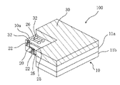
図1に示す半導体モジュール100は、半導体素子30とフィルム部材10とから成っている。半導体素子30は、その表面30aに素子電極32を有している。なお、本明細書では、そのように半導体素子30の素子電極32が形成される表面30aを主面と呼ぶ。フィルム部材10は、絶縁樹脂層11と配線パターン20とから成っており、絶縁樹脂層11の裏面10b(即ち、フィルム部材の裏面)に配線パターン20が形成された態様を有している。なお、かかる配線パターン20は、裏面10bにおいて絶縁樹脂層11に埋め込まれていてもよく、かかる場合、配線パターン20の表面が、好ましくは絶縁樹脂層11の裏面と面一(または略面一)となっていることが好ましい。
A
半導体モジュール100は、図1に示すように、半導体素子30の主面30aとフィルム部材の表面(即ち、絶縁樹脂層の表面)10aとが接するように、半導体素子30とフィルム部材10とが重ねられて構成されており、フィルム部材10の配線パターン20の一部分22が、絶縁樹脂層11を貫通した状態で半導体素子30の素子電極32に接触している。
As shown in FIG. 1, in the
本発明の半導体モジュール100に用いられる半導体素子30は、例えば半導体ベアチップまたはチップ・サイズ・パッケージ(CPS)であってよい。かかる半導体素子30の厚さは、例えば20〜400μmであってよく、好ましくは50〜400μmである。より具体的には、半導体素子30は、メモリICチップ、ロジックICチップまたはシステムLSIチップであってよく、更には発光ダイオード(LED)チップであってもよい。
The
本発明の半導体モジュール100の主面30aに形成される素子電極32は、AlまたはAuから形成されることが好ましく、その厚さは例えば0.01〜0.1μmであってよく、好ましくは0.05〜0.1μmである。
The
本発明の半導体モジュール100に用いられるフィルム部材10の絶縁樹脂層11は、一般的な半導体モジュールに用いられる絶縁樹脂から形成されるものであってよいが、好ましくは透明な絶縁樹脂から形成されている。従って、本実施形態では、絶縁樹脂層11はポリイミドまたはアラミドから成るフィルム(またはコアフィルム)であることが好ましい。なお、絶縁樹脂層11は、ポリフェニレンサルファイド(PPS)、ポリプロピレンまたはポリメタクリル酸メチルから形成してもよい。絶縁樹脂層11の厚さは、例えば1〜30μmであり、好ましくは1〜10μmである。
The insulating
本発明の半導体モジュール100に用いられるフィルム部材10の配線パターン20は、例えば銅から形成されることが好ましく、その厚さは、好ましくは1〜35μmであり、より好ましくは1〜12μmである。
The
図1に示す態様の半導体モジュール100では、フィルム部材10の表面10aおよびそれに対向する裏面10bの寸法は、半導体素子32の主面30aの寸法と略同じとなっており、半導体素子30の主面30aとフィルム部材の表面10aとが接するように、半導体素子30とフィルム部材10とが重ねられている。かかるフィルム部材10の表面10aおよび裏面10bの寸法は、例えば1〜10mm×1〜10mmであり、好ましくは3〜10mm×3〜10mmである。従って、半導体素子30の主面30aの寸法も同様に、例えば1〜10mm×1〜10mmであり、好ましくは3〜10mm×3〜10mmである。
In the
図1に示す半導体モジュール100では、配線パターン20の一部分22が例えばニードル状部材で押圧されることによって、当該配線パターン20の一部分22が絶縁樹脂層11の内部に押し込まれ、その結果、当該配線パターン20の一部分22が絶縁樹脂層11を貫通した状態となっている。従って、かかる配線パターンの一部分の断面は、略U形状となり得るものの、配線パターン20の一部分22が絶縁樹脂層の内部へと押し込まれる態様に応じて種々の形状となり得る。
In the
なお、半導体モジュール100では、配線パターン20の一部分22と半導体素子30の素子電極32とが相互に接触しており、好ましくは接合または圧接されている。従って、かかる接触、接合または圧接により形成される接合部位25は、半導体素子20の素子電極32とフィルム部材10の配線パターン20とを電気的に接続する機能を有する。それゆえ、本明細書では、かかる接合部位25を「層間接続部位」ともいう。そして、上述したように、フィルム部材10は、半導体素子30を基準にすると配線基板(例えば、マザーボード)との中間基板の役割を有するので、フィルムインターポーザ(またはフィルム製インターポーザ)と称することができる。従って、本発明のフィルムインターポーザは、絶縁樹脂層から成るシート状のフィルム(例えば、透光性のフィルム)11と、フィルム11の一方の面に形成された配線パターン20とから構成されており、配線パターン20の一部分22が、フィルム11を貫通した状態でフィルム11の表面(10a)に露出した態様を有している。フィルム11を貫通した配線パターン20の一部分22の断面は略U形状を有しており、当該略U形状の底部が半導体素子30の素子電極32に接触または接続されることになる。
In the
このように、本実施形態の半導体モジュール100は、フィルムインターポーザ10を用いた接続方法であり、上述した従来のワイヤボンディング法、フリップチップボンディング法およびTAB法とは異なる新たな接続方法となっている。
Thus, the
以下、上述の本発明の半導体モジュールの応用例または変更例等について説明する。 Hereinafter, application examples or modifications of the above-described semiconductor module of the present invention will be described.
本実施形態の半導体モジュール100では、フィルム部材10の裏面に半田ボール40を形成することができる。なお、かかる半田ボール40は二次元的に配列されることが好ましい。半田ボール40は、図2に示すように、フィルムインターポーザ10の配線パターン20のランド24に載置してよい。半導体モジュール100は、かかる半田ボール40を介して、配線基板(図2では図示せず)に実装されることになる。なお、半田ボール40が載置されるランド24は、所定の配線(図2では図示せず)を介して、略U形状の層間接続部位25と電気的に接続されている。
In the
かかる図2に示す態様において、フィルムインターポーザ(即ち、フィルム部材)10の寸法は、半導体素子30の主面30aの寸法よりも大きくなるように設計されている。そのため、半導体素子30の素子電極32のピッチよりも広い間隔を、フィルムインターポーザ10のランド24で実現することができ、いわゆるファンアウトを容易に実行することができる。なお、かかる態様のフィルム部材10の表面10aおよび裏面10bの寸法は、例えば3〜15mm×3〜15mmであり、好ましくは5〜15mm×5〜15mmである。その一方、半導体素子30の主面30aの寸法は、例えば3〜15mm×3〜15mmであり、好ましくは5〜15mm×5〜15mmの範囲で設定する。
In the embodiment shown in FIG. 2, the dimension of the film interposer (that is, the film member) 10 is designed to be larger than the dimension of the
なお、図1に示す態様では半導体素子30の主面30aと略同じ寸法の表面10aおよび裏面10bを有するフィルムインターポーザ10が用いられているが、かかるフィルムインターポーザ10に対しても半田ボール40を載置することが可能である。その場合、ランド24は、フィルムインターポーザ10の裏面10bに位置する配線パターン20の所定箇所に形成すればよい。
In the embodiment shown in FIG. 1, the
なお、半導体素子30の表面30aと略同じ寸法の表面10aを有するフィルムインターポーザ10であっても、半導体素子30において素子電極12がペリフェラル状に配列されている場合において、フィルムインターポーザ10にてランド24が行列状になるように配線パターン20を形成すれば、半導体素子30の素子電極32のピッチよりも広い間隔を実現することができる。
Even if the
更に、半導体素子30が半導体ベアチップの場合に、ランド24が二次元的(典型的には、行列状)に配列された配線パターン20を有するフィルムインターポーザ10を組み合わせれば、簡便に、PGA(ピン・グリッド・アレイ)パッケージ、または、BGA(ボール・グリッド・アレイ)パッケージを実現することができる。なお、図1に示す構成を有する半導体モジュール100の場合では、簡便にCSP(例えば、BGA型CSP)にすることも可能である。
Further, when the
図3に示す半導体モジュール100では、例えば図1に示すようなフィルム部材10の裏面に接するように、更なるフィルム部材が積層した態様が示されている。従って、かかる半導体モジュール100は、多層のフィルムインターポーザ10を有している。かかるフィルムインターポーザ10は、第1フィルム11aと第2フィルム11bとから構成されている。第1フィルム11aおよび第2フィルム11bとも、配線パターン20が形成されており、各配線パターン20には層間接続部位25が形成されている。フィルムインターポーザ10の裏面10bには、ランド24が形成されており、かかるランド24に半田ボール40が載置されている。なお、かかる態様を有する半導体モジュールでは、半導体素子が半導体ウェハであることが好ましい。
In the
図4は、本発明の半導体モジュール100の一例の構成を模式的に示した一部切り欠き斜視図である。かかる態様のフィルムインターポーザ10は、第1フィルム11aと第2フィルム11bとから成る多層構造を有している。なお、図示される半導体モジュール100では、フィルムインターポーザ10の表面10aの寸法と、半導体素子30の表面30aの寸法とは略同じになっている。
FIG. 4 is a partially cutaway perspective view schematically showing the configuration of an example of the
図4に示す構成では、層間接続部位25の構造が示されている。なお、理解しやすいように半導体素子30の素子電極32をフィルムインターポーザ10側に明示している。図4に示すように、フィルムインターポーザ10の表面10aに配線(または配線パターン)26を形成して、かかる面10aで電気的な線路を形成することが可能である。
In the configuration shown in FIG. 4, the structure of the
図5も、図4と同様に、半導体モジュール100の一例の構成を模式的に示した一部切り欠き斜視図である。かかる図では、層間接続部位25の構造を見やすいように、フィルムインターポーザ10の外縁領域の一部を切り欠いて示している。図5に示す半導体モジュール100は、端子が100ピン以上のBGAモジュール(またはPGAモジュール)であり、半導体素子30の素子電極が、フィルムインターポーザ10によってファンアウトされている。
FIG. 5 is also a partially cutaway perspective view schematically showing an example of the configuration of the
なお、かかる図5に示す態様では、層間接続部位25の配線パターン20の一部分22を、フィルムインターポーザ10の表面10aに直接露出させるのでなく、フィルムインターポーザ10の表面10aに端子(例えば、ランド)28を形成し、かかる端子28を介して配線パターン20の一部分22を露出させている。かかる端子28は、フィルムインターポーザ10の表面10aに形成された配線26に接続されている。なお、半導体素子30の表面30aが位置する領域では、直接、配線パターン20の一部分22を露出させて半導体素子の素子電極に接合すればよい。
In the embodiment shown in FIG. 5, a
図5に示す態様では、フィルムインターポーザ10の表面10aに配線26および端子28を形成してファンアウトを行っているが、フィルムインターポーザ10の表面10aに配線26および端子28を形成せずに、層間接続部位25を介して、フィルムインターポーザ10の裏面10bの配線パターン20によってファンアウトを行うことも可能である。
In the embodiment shown in FIG. 5, the
なお、層間接続部位に関して説明すると、層間接続部位25を構成する配線パターン20の一部分22は、配線パターン20と継ぎ目なく同一材料で連続して形成されているので、例えば層間接続部位25が導電性ペーストのようなビアから構成されている場合と比較すると、ビア(層間接続部位)と配線(配線パターン)との間のインピーダンスの不整合の問題を回避することができるようになっている。また、配線パターン20と層間接続部位25を構成する一部分22とは同じ材料から構成されているので、双方の熱膨張係数が等しく、接続信頼性に優れている。
The interlayer connection part will be described. Since the
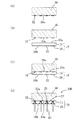
次に、図1に示す半導体モジュール100を製造するための工程断面図を示す図6(a)〜(d)を参照しながら、本発明の半導体モジュール100の製造方法を説明する。
Next, a method for manufacturing the
まず、図6(a)に示すように、主面30aに素子電極32が形成された半導体素子(例えばベアチップ)30を用意する。次いで、図6(b)に示すように、半導体素子30と組み合わせるフィルム部材10’を用意する。かかるフィルム部材10’の裏面10bには、配線パターン20が形成されており、配線パターン20の一部分22が、半導体素子30の素子電極32に対応して形成されている。
First, as shown in FIG. 6A, a semiconductor element (for example, a bare chip) 30 having an
次に、図6(c)に示すように、半導体素子30の表面30aと、フィルム部材10’の表面10aとを接触させるように、半導体素子30とフィルム部材10’とを重ね合わせる。その後、図6(d)に示すように、フィルム部材10’の配線パターン20の一部分22を、フィルム部材10’の絶縁樹脂層11の内部に押し込んで、かかる絶縁樹脂層11を貫通させることによって、配線パターン20の一部分を半導体素子30の素子電極32に接合させる。かかる態様では、例えばニードル状部材等の圧接ツール50を用いて、配線パターン20の一部分22をフィルム部材10’の絶縁樹脂層11の内部に押し込んでいる。従って、形成される層間接続部位25の断面は、略U形状を有している。なお、ニードル状部材の場合は、その押圧部(即ち先端部)が半球面を有していることが好ましく、その直径は例えば10〜200μmであり、好ましくは10〜50μmである。なお、かかるニードル状部材の押圧部が平面状であってもかまわない。
Next, as shown in FIG. 6C, the
以上の工程により、本実施形態の半導体モジュール100を得ることができる。なお、図6(d)に示すように、かかる半導体モジュール100の製造方法では、フィルムインターポーザ10も得ることができることを理解されよう。
The
本実施形態において、フィルム部材10’のフィルム11は、例えばポリイミドまたはアラミドから成り、実質的に透明となっている。従って、半導体素子30とフィルム部材10’とを重ね合わせる工程において素子電極32と配線パターン20の一部分22との位置合わせを実施するに際して、素子電極32をフィルム11越しに見ることが可能であり、かかる位置合わせが容易となっている。
In this embodiment, the
また、圧接ツール50による接合の際に、超音波を印加することも可能である。かかる超音波の印加によって、層間接続部位25の接触箇所または接合箇所は、超音波接合され得、従って、接続信頼性がより良好な半導体モジュールを製造することができる。例えば圧接ツール50に超音波印加機能を設けた場合には、圧接ツール50によって押込みと超音波接合とを同時に実施することができる。なお、超音波の印加による接合をより強固なものにするために、例えば配線パターンを成す銅とは別の金属(例えば、アルミニウム、金、銀、プラチナまたはバナジウムなど)を配線パターン20の一部分22の周囲に設けてよく、その結果、超音波を用いた層間接続部位25の形成に際して、複数の種類の金属が溶融して成る合金を層間接続部位25に存在させることが可能となる。
In addition, it is possible to apply ultrasonic waves when joining with the
なお、印加される超音波の周波数は、例えば40KHz〜1MHzであり、好ましくは40〜800kHzである。また、印加させる超音波の出力パワーは、例えば10〜50Wであり、好ましくは、20〜40Wである。更に、印加時間は、例えば0.1〜1(s)であり、好ましくは0.1〜0.5(s)である。 The frequency of the applied ultrasonic wave is, for example, 40 KHz to 1 MHz, and preferably 40 to 800 kHz. Moreover, the output power of the ultrasonic wave to apply is 10-50W, for example, Preferably, it is 20-40W. Furthermore, application time is 0.1-1 (s), for example, Preferably it is 0.1-0.5 (s).
なお、超音波の印加は、配線パターン20の一部分の物理的特性を測定しながら実行することが好ましい。そのような物理的特性としては、配線パターン20の一部分の抵抗値または配線パターンの絶縁部材に対する押込み量等が挙げられる。例えば抵抗値等の物理的特性を測定しながら、超音波接合を行うと、層間接続部位25の強度をリアルタイムで知ることができ、当該強度が所望の値となるまで超音波を印加することが可能となる。また、物理的特性を測定しながらの超音波の印加は、最初の一回または数回のみの実施で足り得、以後は、それから得られる結果を用いることによって、例えば印加時間または超音波のエネルギー量等を調整することができる。
The application of ultrasonic waves is preferably performed while measuring the physical characteristics of a part of the
上述の本発明の半導体モジュールおよびその製造方法では、配線パターン20の一部分22の接合によって半導体素子30との電気的な接続を確保するので、ワイヤボンディング法のように一つずつ金属細線(金ワイヤ)を用いて結線しなくてもよい。従って、ワイヤボンディング法と比べて作業の手間を軽減させることができる。更に詳細に説明すると、半導体素子のピン数(入出力端子数)は近年大幅に増加する傾向を有しており、当該ピン数は2006年には1000ピン、2010年には2000ピンにまで達すると言われている。従って、そのような多ピン化する半導体素子に対して、ワイヤボンディング法を用いて一つずつ結線するのは非常に手間であるのに対し、本発明の半導体モジュールおよびその製造方法では、例えば複数のニードル状部材で一括して層間接続部位を形成することができるので、そのような問題に対処することができるようになっている。
In the above-described semiconductor module and the manufacturing method thereof according to the present invention, since the electrical connection with the
また、本発明の半導体モジュールおよびその製造方法では、配線パターン20によってピッチを規定できるので、ワイヤボンディング法と比べて、より微細なピッチで接続を行うことができる。半導体素子30のピンのピッチは、2006年には40μm、2010μmには20μmにまで達すると言われており、金ワイヤの直径等を考慮すれば、ワイヤボンディング法を用いてそのような微細ピッチに対応するのは非常に困難となり得るか、または事実上不可能となり得る。一方、本発明の半導体モジュールおよびその製造方法では、配線パターンによってピッチを規定することができるので、そのような微細ピッチに対応することが容易となっている。
Further, in the semiconductor module and the manufacturing method thereof according to the present invention, since the pitch can be defined by the
更に、本発明の半導体モジュールおよびその製造方法では、半導体素子(例えばベアチップ)の周囲の適切な範囲にフィルムインターポーザを配置すればよいので、ワイヤボンディング法で製造される半導体モジュールと比べて、実装面積も小さくすることができる。例えば、図1に示す半導体モジュール100では、半導体素子(ベアチップ)30の主面30aと同じ寸法のリアルサイズのCSPを実現することができる。また、フィルムインターポーザ10によって接続を行うので、ワイヤボンディング法と比べて、高さがより低い半導体モジュールを得ることができる。従って、半導体モジュールの薄型化に寄与し得ることになる。
Furthermore, in the semiconductor module and the manufacturing method thereof according to the present invention, the film interposer may be disposed in an appropriate range around the semiconductor element (for example, a bare chip), so that the mounting area is larger than that of the semiconductor module manufactured by the wire bonding method. Can also be reduced. For example, in the
また、本実施形態の構成の場合、半導体素子30とフィルム部材10’とを重ね合わせる際に透明なフィルム11を通して半導体素子30の素子電極32の位置を確認することができるので、フリップチップボンディング法と比較して、位置合わせを容易に行うことができる。従って、フリップチップボンディング法よりも、半導体素子との実装公差ズレを減少させることがより容易となっている。
Further, in the case of the configuration of the present embodiment, the position of the
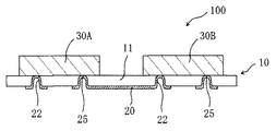
特に、図7に示すように、半導体素子30の裏面30b(主面30aと対向する面)を配線基板41の上に載置すると共に、フィルムインターポーザ(即ちフィルム部材)10の配線パターン20の一部分23が絶縁樹脂層を貫通して配線基板41の電極42に電気的に接続する構成を有する半導体モジュールの場合、素子電極32との位置合わせも、配線基板41の電極42との位置合わせも、透明なフィルム11を通して目視確認により行うことができるので、技術的な価値が高い。ここで、目視による確認とは、作業者の目による確認だけでなく、画像認識装置(例えば、CCDやCMOSセンサーを含む装置)による確認も含んでいる。なお、かかる図7に示す態様では、半導体モジュール100は、
素子電極32を有する主面30aおよび前記主面30aに対向する裏面30bを有する半導体素子30と、
表面10aおよび当該表面10aに対向する裏面10bを有する絶縁樹脂層11から成り、前記絶縁樹脂層の裏面10bに配線パターン20が形成されているフィルム部材10と、
配線基板41と
を備えており、
半導体素子30の裏面30bが配線基板41と接するように、半導体素子30が配線基板41に載置されており、
フィルム部材10の表面10aおよび裏面10bの寸法は、半導体素子30の主面30aの寸法よりも大きく、半導体素子30の主面30aとフィルム部材10の表面10aとが接するように、フィルム部材10が半導体素子30に載置されていると共に、フィルム部材10の少なくとも一部分が配線基板41上にまで延在しており、
フィルム部材10の配線パターン20の一部分22の少なくとも1つが、前記絶縁樹脂層11を貫通した状態で半導体素子30の素子電極32に接触している一方、フィルム部材10の配線パターン20の一部分の残り23の少なくとも1つが、絶縁樹脂層11を貫通した状態で配線基板41上に形成された電極42に接触している。
In particular, as shown in FIG. 7, the
A
A
A
The
The dimension of the
At least one
更に、フリップチップボンディング法の場合、半導体素子の電極形成面が配線基板の方を向いてしまうので、半導体素子と配線基板との接続状況を目視により確認することが困難であるが、例えば図7に示す構成を有する半導体モジュールでは、半導体素子30と配線基板41との接続の確認が容易に行うことができるようになっている。
Furthermore, in the case of the flip chip bonding method, since the electrode formation surface of the semiconductor element faces the wiring board, it is difficult to visually confirm the connection state between the semiconductor element and the wiring board. In the semiconductor module having the configuration shown in FIG. 8, the connection between the
更に、本発明の半導体モジュールおよびその製造方法では、フリップチップボンディング法で配線基板に形成されるファインパターンをフィルムインターポーザ(即ちフィルム部材)の配線パターンに形成すればよいので、フリップチップボンディング法と比べて、配線基板のコストアップを抑制することができる。また、フリップチップボンディング法の場合には特定の領域(即ち、半導体素子の主面と対向する配線基板の領域)に数多くの端子が集中することに伴って、配線基板の層数を多くしなければならない場合が多かったが、本発明の半導体モジュールおよびその製造方法では、フィルムインターポーザの配線パターンによって配線の引き回しを行うことができるので、フリップチップボンディング法の場合と比べて配線基板の層数を少なくすることができる。従って、かかる理由からも配線基板のコストアップを抑制することができる。なお、図3および図4に示すように、フィルムインターポーザ10自体の多層化も比較的容易に実現することが可能となっている。また、図2、図3および図5に示すように、フィルムインターポーザ10によるファンアウトによって、配線基板41のファインピッチ(または微細ピッチ)の度合いを下げてコストアップを抑えることも可能である。
Furthermore, in the semiconductor module and the manufacturing method thereof according to the present invention, the fine pattern formed on the wiring board by the flip chip bonding method may be formed on the wiring pattern of the film interposer (that is, the film member). Thus, an increase in the cost of the wiring board can be suppressed. In the case of the flip chip bonding method, the number of layers of the wiring board must be increased as a large number of terminals are concentrated in a specific area (that is, the area of the wiring board facing the main surface of the semiconductor element). In many cases, the semiconductor module of the present invention and the manufacturing method thereof can route the wiring by the wiring pattern of the film interposer. Therefore, the number of layers of the wiring board is smaller than that in the case of the flip chip bonding method. Can be reduced. Therefore, an increase in the cost of the wiring board can also be suppressed for this reason. As shown in FIGS. 3 and 4, the
更に、本発明の半導体モジュールおよびその製造方法では、フリップチップボンディング法での半導体素子と配線基板との線熱膨張係数のマッチングと比べて、半導体素子30とフィルムインターポーザ10との線熱膨張係数のマッチングの必要性が比較的緩和されている利点を有する。即ち、本発明のフィルムインターポーザ(又はフィルム)は薄いので半導体素子に大きい影響をあまり与えない。また、フィルムの可撓性によって線熱膨張係数の差異に起因する応力を吸収することも可能となっている。
Furthermore, in the semiconductor module of the present invention and the manufacturing method thereof, the linear thermal expansion coefficient between the
そして、本発明の半導体モジュール(特に、図7に示す構成を有する半導体モジュール)およびその製造方法では、フリップチップボンディング法で使用されるアンダーフィル剤(封止樹脂)を用いずに、半導体素子と配線基板との接続を行うことができるので、その点でも有利である。また、本発明の半導体モジュールでは、フィルムインターポーザによって、素子電極が形成された半導体素子の主面を保護することができる。 In the semiconductor module of the present invention (particularly, the semiconductor module having the configuration shown in FIG. 7) and the manufacturing method thereof, the semiconductor element and the underfill agent (sealing resin) used in the flip chip bonding method are used. Since it can connect with a wiring board, it is advantageous also in that respect. Moreover, in the semiconductor module of this invention, the main surface of the semiconductor element in which the element electrode was formed can be protected with a film interposer.
なお、本発明の半導体モジュールおよびその製造方法において、半導体素子の素子電極は、バンプ(例えば、半田バンプまたは金バンプ)が形成されたものを使用してよいし、または、バンプが形成されていないものを使用してもよい。従って、フリップチップボンディング法の場合と異なって、素子電極にバンプを形成せずに、半導体素子と配線基板とを電気的に接続することができる。 In the semiconductor module and the method for manufacturing the same according to the present invention, the element electrode of the semiconductor element may be a bump on which a bump (for example, a solder bump or a gold bump) is formed, or no bump is formed. Things may be used. Therefore, unlike the flip chip bonding method, the semiconductor element and the wiring board can be electrically connected without forming bumps on the element electrodes.
次にTAB法の場合との比較について検討する。かかるTAB法ではインナーリード工程とアウターリード工程とを別々に実施する必要があったが、本発明の半導体モジュールの製造方法では、そのような別々の工程を実施しなくてもよい。更に、本発明の半導体モジュールでは、TAB法のように封止樹脂を用いなくてもよく、加えて、実装面積も小さくすることができる。 Next, the comparison with the case of the TAB method will be examined. In such a TAB method, the inner lead process and the outer lead process need to be performed separately. However, in the method for manufacturing a semiconductor module of the present invention, such separate processes need not be performed. Furthermore, in the semiconductor module of the present invention, it is not necessary to use a sealing resin as in the TAB method, and in addition, the mounting area can be reduced.
なお、図1等に示す例では、分かり易いように、素子電極12の数が少ないものを示したが、素子電極12の数は特に限定されていない。図6(d)に示すような圧接ツール50を用いれば、素子電極12が多い場合であっても、一括して接合工程を実施することができる。従って、半導体素子の素子電極が多ければ多いほど、本発明の半導体モジュールは、例えばワイヤボンディング法と比べて技術的価値が高くなる。また、本明細書では素子電極がペリフェラル状に配列した半導体素子の例を多く示したが、これに限定されず、アレイ状に配列した半導体素子を用いることも可能である。更に、図7に示す構成を有する半導体モジュールでは、素子電極32との接合にのみ略U形の層間接続部位25を用いる一方、配線基板41の電極42との接合には、他の公知の接合手法(例えば、はんだなどの低融点金属)を用いることも可能である。
In the example shown in FIG. 1 and the like, the number of element electrodes 12 is small for easy understanding, but the number of element electrodes 12 is not particularly limited. If a
次に、図8〜図12を参照しながら、本発明の半導体モジュールの別の製造方法およびそれにより得られる半導体モジュールについて説明する。 Next, another method for manufacturing a semiconductor module of the present invention and a semiconductor module obtained by the method will be described with reference to FIGS.
図6(a)〜(d)を参照して説明した製造方法では、絶縁樹脂層11に配線パターン20が形成されたフィルム部材10’を用いたが、そのような態様に限らず、半導体素子30の主面30aに絶縁樹脂を塗布して、その塗布膜を絶縁樹脂層11として使用することも可能である。以下、その手法について説明する。
In the manufacturing method described with reference to FIGS. 6 (a) to 6 (d), the
まず、図8(a)に示すように、主面30aに素子電極32を有する半導体素子30と、キャリアシート18上に形成された金属層(典型的には銅箔)19とを用意する。ここでキャリアシートは、例えばPET(ポリエチレンテレフタレート)、PEN(ポリエチレンナフタレート)から形成されることが好ましく、その厚さは、例えば5〜15μmである。
First, as shown in FIG. 8A, a
次に、図8(b)に示すように、キャリアシート18上の金属層19をパターニングして、配線パターン20を形成すると共に、半導体素子30の主面30aには素子電極32が覆われるように絶縁樹脂を塗布して塗布膜11’を形成する。なお、絶縁樹脂は、粘着材または接着層が好ましい。次いで、矢印60に示すように、キャリアシート18上の配線パターン20を塗布膜11’に転写すると、図8(c)に示すように、半導体素子30の主面30a上に、配線パターン20を有するフィルム部材10’が形成されることになる。
Next, as shown in FIG. 8B, the
その後、図9(a)に示すように、配線パターン20の一部分22を圧接ツール50で塗布膜11’内部へと押し込み、層間接続部位25を形成すると、図9(b)に示すような形態の半導体モジュール100が得られる。
Thereafter, as shown in FIG. 9A, when a
かかる製造方法は、塗布膜11’によってフィルム11を形成するので、予め、配線パターン20付きのフィルム部材10’を用意しておく必要がなく、従って、転写工程を行うことができる設備が完備されていれば、比較的便利な手法となり得る。
In this manufacturing method, since the
また、転写工程を用いて本発明の半導体モジュールを製造する場合、図10(a)〜図12(b)に示すような方法で製造することも可能である。 Moreover, when manufacturing the semiconductor module of this invention using a transcription | transfer process, it is also possible to manufacture by the method as shown to Fig.10 (a)-FIG.12 (b).
まず、図10(a)に示すようなキャリアシート18上の金属層19をパターニングして、図10(b)に示すような配線パターン20を得る。次いで、その配線パターン20を矢印60に示すように、フィルム11B上に形成された絶縁樹脂層11Aへと転写して、配線パターン20が形成されたフィルム部材10’を形成する。絶縁樹脂層11Aは、接着層または粘着層が好ましく、例えばエポキシから成るものであってよい。その一方、フィルム11Bは、例えば、ポリイミドまたはアラミドから成るものであってよい。
First, the
それと並行して、図11(a)に示す半導体素子30を用意し、その主面30a上に絶縁樹脂層11Cを形成し、かかる樹脂層によって素子電極32を覆う(図11(b)参照)。絶縁樹脂層11Cは、接着層または粘着層が好ましく、例えばエポキシから成るものであってよい。
In parallel with this, the
次いで、図12(a)に示すように、フィルム部材10’のフィルム11Bを、樹脂層11Cの上に載せた後、図12(b)に示すように、圧接ツール50によって層間接続部位25を形成すれば半導体モジュール100を作製することができる。
Next, as shown in FIG. 12A, after the
なお、図11(b)に示した工程を経ずに、図10(c)に示したフィルム部材10’のフィルム11Bの下面(露出面)に絶縁樹脂層11Cを形成し、次いで、それを半導体素子30の主面30a上に載せて、図12(a)に示す構造を有する半導体モジュール100を形成してもよい。
In addition, without passing through the process shown in FIG. 11B, the insulating
かかる態様では、上述したように、フィルム11Bとしてアラミドフィルムを用いることが好ましい。これは、ポリイミドフィルムよりも、所定強度において薄いフィルムを実現し易いからであり、また、アラミドフィルムは、ポリイミドフィルムよりも安価であるからである。更に詳細に説明すると、アラミドフィルムは、ポリイミドよりも高弾性強度を有しており、薄層化に適している。例えば、厚さが約12.5μmのポリイミドフィルムの強度に相当するアラミドフィルムの厚さは約4μmである。また、アラミドは低コストであることに加えて、低吸湿を有しており、寸法変化が少ないという利点も兼ね備えている。
In this aspect, as described above, it is preferable to use an aramid film as the
なお、ポリイミドフィルムは耐熱性に優れているので、耐熱性が要求される場合には、アラミドフィルムよりもポリイミドフィルムを用いた方が好ましい。 In addition, since a polyimide film is excellent in heat resistance, when heat resistance is requested | required, it is more preferable to use a polyimide film rather than an aramid film.
上記転写工程を用いた製造方法によると、配線パターン20は、転写により樹脂層11(または11A)に埋設されて形成されるので、平担性に優れているという利点を有している。なお、上記例では、転写法を用いた銅箔から成る配線パターン20を形成するので、ウエットエッチングを用いて形成した配線パターンよりもファインピッチなものにすることができるという別の利点も有している。例えば、ウエットエッチングを用いて形成した配線パターンのライン/スペース(L/S)が40μm/40μm程度である場合に、転写法を用いた配線パターンのL/Sは15μm/15μm(30μmピッチ)にまで微細化することが可能である。
According to the manufacturing method using the transfer step, the
ただし、このことは、ウエットエッチングを用いてパターニングされた配線パターン20を用いることができないことを意味していない。例えば、図6(b)に示すフィルム部材10’を、フィルム11上に銅層(金属層)が積層された銅張積層板(CCL)に対してエッチングを施して作製することも可能である。銅張積層板(CCL)には、フィルム11の上に直接、銅層が形成されたもの(二層CCL)、または、接着層を介して銅層が形成されたもの(三層CCL)があるが、双方とも利用することができる。なお、銅張積層板(CCL)を用いた場合には、銅張積層板自体が典型的なフレキシブル基板の製造に多く使用されており、一般に流通しているので、材料のコストダウンが達成され得るという利点がある。
However, this does not mean that the
(実施形態2)
次に、図13〜図17を参照しながら、本発明の実施形態に係る更なる改変例について説明する。なお、説明を簡素化するために、上記実施形態1と同様の点については省略または簡略する。
(Embodiment 2)
Next, further modifications according to the embodiment of the present invention will be described with reference to FIGS. In order to simplify the description, the same points as in the first embodiment are omitted or simplified.
上記実施形態1では、1つのフィルムインターポーザ10の上に1つの半導体素子30を搭載したが、図13に示すように、1つのフィルムインターポーザ10に複数の半導体素子30Aおよび30Bを搭載して、本発明の実施形態に係る半導体モジュール100をマルチチップモジュールにすることも可能である。
In the first embodiment, one
図13に示す構成では、フィルムインターポーザ10に形成された連続した配線パターン20によって、半導体素子30Aと半導体素子30Bとを接続することができる。従って、フィルムインターポーザ10によるLSIチップ間の高速配線接続を実現することが可能となっており、高性能な機能をもつモジュールを実現できるという利点を有している。なお、図13では素子電極32が省略して描かれている。
In the configuration shown in FIG. 13, the
図13に示した例では、半導体素子30Aと30Bとの組み合わせを示したが、半導体素子30Aと受動部品とを組み合わせた半導体モジュール100を実現することも可能である。また、図13に示す例に受動部品を組み合わせることも可能である。
In the example shown in FIG. 13, the combination of the
また、図14に示すように、図13に示す半導体モジュール100を通常のインターポーザ45を介して配線基板41に実装することも可能である。ここでは、半導体素子30Aと30Bとの相互の信号のやり取りは、フィルムインターポーザ10の配線パターン20を介して行っており、高速処理が実現されている。かかる箇所以外の少なくとも一部の電気的なやり取りは、インターポーザ45及び配線基板41を介して実行することが可能となる。なお、フィルムインターポーザ10によって既に一度ファンアウトがなされているので、通常のインターポーザ45のファインピッチの度合いを下げて、コストを下げることが可能となる。
Further, as shown in FIG. 14, the
また、フィルムインターポーザ10は、図15に示すように用いることもできる。即ち、図15に示す例では、半導体素子30Aおよび30Bの裏面30b同士を合わせた態様となっており、半導体素子30Aと30Bとの電気的接続がフィルムインターポーザ10によって行われている。フィルムインターポーザ10は、半導体素子30Aおよび30Bの側面30cの周囲を経由して半導体素子30Aの表面から半導体素子30Bの表面まで延在しており、フィルムインターポーザ10の配線パターン20の一部分22が、絶縁樹脂層11の内部に押し込まれることによって半導体素子30Aおよび30Bの素子電極(図示せず)に接続されている。
The
従って、別の見方をすれば、図15に示す半導体モジュール100は、
主面および裏面に素子電極を有する半導体素子(即ち、両面に素子電極を有する半導体素子)と、
表面および裏面を有する絶縁樹脂層から成り、その裏面に配線パターンが形成されているフィルム部材と
を備えており、
フィルム部材が、半導体素子の主面から半導体素子の側面を経由して半導体素子の裏面に延在するように、フィルム部材の表面と、半導体素子の主面および裏面とが接しており、
フィルム部材の配線パターンの一部分は、絶縁樹脂層を貫通した状態で半導体素子の主面および裏面の素子電極に接している。
Therefore, from another viewpoint, the
A semiconductor element having element electrodes on the main surface and the back surface (that is, a semiconductor element having element electrodes on both surfaces);
It comprises an insulating resin layer having a front surface and a back surface, and a film member having a wiring pattern formed on the back surface.
The surface of the film member is in contact with the main surface and the back surface of the semiconductor element so that the film member extends from the main surface of the semiconductor element to the back surface of the semiconductor element via the side surface of the semiconductor element.
A part of the wiring pattern of the film member is in contact with the element electrodes on the main surface and the back surface of the semiconductor element in a state of penetrating the insulating resin layer.
なお、かかる図15に示すような半導体モジュールおよびフィルムインターポーザは、図6(a)〜(d)の製造方法で得られる半導体モジュールおよびフィルムインターポーザと同様の特徴を有し、それらの応用例または変更例等についても同様であることを理解されよう。従って、かかる同様の点については省略または簡略する。 The semiconductor module and the film interposer as shown in FIG. 15 have the same characteristics as those of the semiconductor module and the film interposer obtained by the manufacturing method shown in FIGS. 6 (a) to 6 (d). It will be understood that the same applies to the examples. Accordingly, such similar points are omitted or simplified.
図3を参照して説明したように、本実施形態のフィルムインターポーザ10は、多層化することが比較的容易であり、図16に示すように、各層のフィルム11に形成された配線パターン20を層間接続部位25で接続することによって、多層のフィルムインターポーザ10を形成することができる。
As described with reference to FIG. 3, the
更に、図16に示す構成を有するフィルムインターポーザ10は、個片の半導体素子30にだけ搭載されるのではなく、複数の半導体素子(ベアチップ)が配列された半導体ウェハ上にも搭載することができる。ベアチップ30が個片に切断される前の半導体ウェハ35にフィルムインターポーザ10を搭載すれば、ウェハレベルCSP(WL−CSP)を簡便に製造することができ、利便性が非常に高くなる。
Furthermore, the
以上、本発明を好適な実施形態により説明してきたが、こうした記述は限定事項ではなく、勿論、種々の改変が可能である。 As mentioned above, although this invention was demonstrated by suitable embodiment, such description is not a limitation matter and of course various modifications are possible.
なお、本発明の実施形態の半導体モジュールと本質的に構成を異にするものであるが、関連する構造を有するものとして、特開平4−283987号公報に開示された電子回路装置がある。その電子回路装置の構造を図18に示す。 An electronic circuit device disclosed in Japanese Patent Application Laid-Open No. 4-283987 is known as a device having a related structure, although the configuration is essentially different from that of the semiconductor module according to the embodiment of the present invention. The structure of the electronic circuit device is shown in FIG.
図18に示す電子回路装置200は、絶縁樹脂層207に埋設された回路素子(例えば、半導体IC)205、206の外部電極端子層205a、206aが配線回路導体層209によって電気的に接続された構造を有している。配線回路導体層209は、無電解めっき法によって形成された金属銅配線であり、直接、外部電極端子層205a、206aに接続されている。なお、符合「208」は接着剤層で、符合「210」は層間絶縁樹脂層である。この電子回路装置200は、いわゆるビルドアップ層の技術が適用されたものであり、同公報には、本発明の実施形態に係る半導体モジュールの層間接続部位に関する技術およびフィルムインターポーザに関する技術は開示されていない。
In the
また同様に、本発明の技術的思想と本質的に異なるものであるが、金属基板(例えば、アルミニウム基板)との電気的な接続を確保するために、ネジを用いずに、配線パターンの一部が絶縁層を突き破って金属基板と接続させるものが、特開平4−283987号公報および特開昭49−27866号公報に開示されている。双方とも、金属基板と接続させるために、接続用工具を用いて、比較的軟らかいアルミニウム基板の表面が完全に変形するまで深く陥没させている。従って、かかる手法を半導体素子の素子電極に対して行うと半導体素子が破壊されてしまうことになる。もちろん、同公報に開示されているものは、ワイヤボンディング法、フリップチップボンディング法およびTAB法のような微細ピッチ接続技術ではなく、ネジによる接続の代替技術であり、本発明の実施形態のものと本質的に異なる技術である。 Similarly, although it is essentially different from the technical idea of the present invention, in order to ensure an electrical connection with a metal substrate (for example, an aluminum substrate), one of the wiring patterns is used without using screws. Japanese Patent Application Laid-Open Nos. 4-283987 and 49-27866 disclose that the portion penetrates the insulating layer and is connected to the metal substrate. In both cases, in order to connect to the metal substrate, the surface of the relatively soft aluminum substrate is depressed deeply using a connecting tool until the surface is completely deformed. Therefore, when such a method is applied to the element electrode of the semiconductor element, the semiconductor element is destroyed. Of course, what is disclosed in the publication is not a fine pitch connection technique such as a wire bonding method, a flip-chip bonding method, and a TAB method, but an alternative technology for connection by screws, and the embodiment of the present invention. It is an essentially different technology.
本発明によれば、ワイヤボンディング法、フリップチップボンディング法およびTAB法とは異なる新規な微細ピッチ接続技術を用いた半導体モジュールおよびその製造方法が提供される。 According to the present invention, a semiconductor module using a novel fine pitch connection technique different from the wire bonding method, the flip chip bonding method, and the TAB method and a manufacturing method thereof are provided.
本発明の半導体モジュールは、その特徴を利用して、極めて実装面積が制限されるような薄型および小型の電子機器に搭載することができる。例えば、携帯電話に搭載することが好ましい。また、携帯電話に限らず、PDAまたはノートパソコンに用いることが可能である。更に、例えば、デジタルスチルカメラまたは薄型テレビ(FPD;フラットパネルディスプレイ))等の他の用途にも適用することが可能である。 The semiconductor module of the present invention can be mounted on a thin and small electronic device whose mounting area is extremely limited by utilizing the feature. For example, it is preferable to be mounted on a mobile phone. Further, the present invention can be used not only for mobile phones but also for PDAs or notebook computers. Furthermore, the present invention can also be applied to other uses such as a digital still camera or a thin television (FPD; flat panel display).
また、半導体素子としてLEDチップを用いると、フィルムインターポーザの配線パターンによって導通が確保され、フィルムを通過して光が出射する半導体モジュールまたは半導体装置(発光デバイス)を構築することができる。 Further, when an LED chip is used as a semiconductor element, it is possible to construct a semiconductor module or a semiconductor device (light emitting device) in which conduction is ensured by the wiring pattern of the film interposer and light is emitted through the film.
更に、半導体素子をLEDチップとした場合に、フィルム内に蛍光体を分散させると、LEDチップからの出射光と蛍光体から発せられる光との双方の光を利用した発光デバイスを構築することができる。なお、本発明の実施形態の半導体モジュールを白色発光デバイスとして利用したい場合、半導体素子として、青色の光を出射する青色LEDチップを用い、そして、フィルムに分散させる蛍光体として、黄色の光に変換する黄色蛍光体を用いればよい。かかる場合、LEDチップとして、窒化ガリウム(GaN)系材料から成るLEDチップ、そして、蛍光体として、YAG系の蛍光体等を好適に用いることができる。 Furthermore, when the semiconductor element is an LED chip, if the phosphor is dispersed in the film, it is possible to construct a light emitting device that uses both the light emitted from the LED chip and the light emitted from the phosphor. it can. If the semiconductor module of the embodiment of the present invention is to be used as a white light emitting device, a blue LED chip that emits blue light is used as the semiconductor element, and it is converted into yellow light as a phosphor dispersed in the film. A yellow phosphor may be used. In this case, an LED chip made of a gallium nitride (GaN) -based material can be suitably used as the LED chip, and a YAG-based phosphor can be suitably used as the phosphor.
また、青色LEDチップを用いるだけでなく、紫外光を発する紫外LEDチップを用いることも可能であり、この場合、紫外LEDチップからの光で励起して、赤(R)、緑(G)および青(B)の光を発する蛍光体をフィルムに分散させるようにすれば、白色発光デバイスを構築することができる。もちろん、白色以外にもLEDチップの種類と蛍光体の種類とを適宜選択することによって所望の色を発する発光デバイスを構築することが可能である。 It is also possible to use not only a blue LED chip but also an ultraviolet LED chip that emits ultraviolet light. In this case, excitation with light from the ultraviolet LED chip causes red (R), green (G) and If a phosphor emitting blue (B) light is dispersed in a film, a white light emitting device can be constructed. Of course, it is possible to construct a light emitting device that emits a desired color by appropriately selecting the type of LED chip and the type of phosphor other than white.
10 フィルムインターポーザ(フィルム部材)
11 絶縁樹脂層
11’塗布膜
12 素子電極
18 キャリアシート
19 金属層
20 配線パターン
22 配線パターンの一部分
24 ランド
25 層間接続部位
26 配線
28 端子
30 半導体素子
30a 半導体素子の主面(電極形成面)
32 素子電極
35 半導体ウェハ
40 半田ボール
41 配線基板
42 配線基板の電極
45 インターポーザ
50 圧接ツール
100 半導体モジュール
200 電子回路装置
205a 外部電極端子層
207 絶縁樹脂層
209 配線回路導体層
500 半導体モジュール(半導体素子部品)
600 半導体デバイス
700 半導体装置。
10 Film interposer (film member)
DESCRIPTION OF
32
600
Claims (35)
表面および当該表面に対向する裏面を有する絶縁樹脂層、ならびに前記絶縁樹脂層の裏面に形成された配線パターンを有するフィルム部材と
を備える半導体モジュールであって、
前記半導体素子の主面と前記フィルム部材の絶縁樹脂層の表面とが接するように、前記半導体素子と前記フィルム部材とが重ねられており、
前記フィルム部材の配線パターンの一部分は、前記絶縁樹脂層を貫通して前記半導体素子の素子電極に接触している、半導体モジュール。 A semiconductor element having a main surface on which an element electrode is formed;
A semiconductor module comprising an insulating resin layer having a front surface and a back surface facing the surface, and a film member having a wiring pattern formed on the back surface of the insulating resin layer,
The semiconductor element and the film member are overlapped so that the main surface of the semiconductor element and the surface of the insulating resin layer of the film member are in contact with each other,
A part of the wiring pattern of the film member is a semiconductor module that penetrates the insulating resin layer and is in contact with an element electrode of the semiconductor element.
表面および当該表面に対向する裏面を有する絶縁樹脂層、ならびに前記絶縁樹脂層の裏面に形成された配線パターンを有するフィルム部材と、
配線基板と
を備える半導体モジュールであって、
前記半導体素子の裏面が前記配線基板と接するように、前記半導体素子が前記配線基板に載置されており、
前記フィルム部材の表面および前記表面に対向する裏面の寸法が、前記半導体素子の主面の寸法よりも大きく、前記半導体素子の主面と前記フィルム部材の絶縁樹脂層の表面とが接するように、前記フィルム部材が前記半導体素子に載置され、前記フィルム部材の少なくとも一部が前記配線基板にまで延在しており、
前記フィルム部材の配線パターンの一部分の少なくとも1つが、前記絶縁樹脂層を貫通した状態で前記半導体素子の素子電極に接触している一方、前記フィルム部材の配線パターンの一部分の残りの少なくとも1つが、前記絶縁樹脂層を貫通して前記配線基板上に形成された電極に接触している、半導体モジュール。 A semiconductor element having a main surface on which an element electrode is formed and a back surface facing the main surface;
An insulating resin layer having a front surface and a back surface facing the surface, and a film member having a wiring pattern formed on the back surface of the insulating resin layer;
A semiconductor module comprising a wiring board,
The semiconductor element is placed on the wiring board such that the back surface of the semiconductor element is in contact with the wiring board;
The dimensions of the front surface of the film member and the back surface facing the front surface are larger than the dimensions of the main surface of the semiconductor element, so that the main surface of the semiconductor element and the surface of the insulating resin layer of the film member are in contact with each other. The film member is mounted on the semiconductor element, and at least a part of the film member extends to the wiring board;
At least one part of the wiring pattern of the film member is in contact with the element electrode of the semiconductor element in a state of penetrating the insulating resin layer, while at least one of the remaining part of the wiring pattern of the film member is A semiconductor module, which penetrates through the insulating resin layer and is in contact with an electrode formed on the wiring board.
表面および当該表面に対向する裏面を有する絶縁樹脂層、ならびに前記絶縁樹脂層の裏面に形成された配線パターンを有するフィルム部材と
を備える半導体モジュールであって、
前記フィルム部材が、前記半導体素子の主面から前記半導体素子の側面を経由して前記半導体素子の裏面に延在するように、前記フィルム部材の絶縁樹脂層の表面と、前記半導体素子の主面および裏面とが接しており、
前記フィルム部材の配線パターンの一部分は、前記絶縁樹脂層を貫通して前記半導体素子の主面および裏面の素子電極に接触している、半導体モジュール。 A semiconductor element having a main surface on which an element electrode is formed and a back surface facing the main surface;
A semiconductor module comprising an insulating resin layer having a front surface and a back surface facing the surface, and a film member having a wiring pattern formed on the back surface of the insulating resin layer,
The surface of the insulating resin layer of the film member and the main surface of the semiconductor element so that the film member extends from the main surface of the semiconductor element to the back surface of the semiconductor element via the side surface of the semiconductor element. And the back is in contact,
A part of the wiring pattern of the film member is a semiconductor module that penetrates through the insulating resin layer and is in contact with element electrodes on a main surface and a back surface of the semiconductor element.
前記配線パターンの一部分は、前記絶縁樹脂層を貫通して他方の面に露出している、フィルムインターポーザ。 An insulating resin layer having a front surface and a back surface facing the surface, and a film interposer in which a wiring pattern is formed on one surface of the insulating resin layer,
A part of the wiring pattern is a film interposer that penetrates the insulating resin layer and is exposed on the other surface.
(b)表面および当該表面に対向する裏面を有する絶縁樹脂層、ならびに前記絶縁樹脂層の裏面に形成された配線パターンを有するフィルム部材を用意する工程と、
(c)前記半導体素子の主面と前記フィルム部材の絶縁樹脂層の表面とが接するように、前記半導体素子と前記フィルム部材とを重ねる工程と、
(d)前記フィルム部材の配線パターンの一部分を前記絶縁樹脂層の内部に押し込んで前記半導体素子の素子電極に接触させる工程と
を含んで成る、半導体モジュールの製造方法。 (A) preparing a semiconductor element having a main surface on which an element electrode is formed;
(B) preparing an insulating resin layer having a front surface and a back surface facing the surface, and a film member having a wiring pattern formed on the back surface of the insulating resin layer;
(C) stacking the semiconductor element and the film member such that the main surface of the semiconductor element and the surface of the insulating resin layer of the film member are in contact with each other;
(D) A method of manufacturing a semiconductor module, comprising a step of pressing a part of the wiring pattern of the film member into the insulating resin layer and bringing it into contact with the element electrode of the semiconductor element.
目視することによって前記工程(d)を実施する、請求項31に記載の半導体モジュールの製造方法。 The film member is transparent,
32. The method for manufacturing a semiconductor module according to claim 31, wherein the step (d) is performed by visual observation.
35. The method of manufacturing a semiconductor module according to claim 34, wherein the physical characteristic is a resistance value of a part of the wiring pattern.
Priority Applications (2)
| Application Number | Priority Date | Filing Date | Title |
|---|---|---|---|
| JP2004318891A JP2006134912A (en) | 2004-11-02 | 2004-11-02 | Semiconductor module and its manufacturing method, and film interposer |
| US11/262,758 US20060091524A1 (en) | 2004-11-02 | 2005-11-01 | Semiconductor module, process for producing the same, and film interposer |
Applications Claiming Priority (1)
| Application Number | Priority Date | Filing Date | Title |
|---|---|---|---|
| JP2004318891A JP2006134912A (en) | 2004-11-02 | 2004-11-02 | Semiconductor module and its manufacturing method, and film interposer |
Publications (2)
| Publication Number | Publication Date |
|---|---|
| JP2006134912A true JP2006134912A (en) | 2006-05-25 |
| JP2006134912A5 JP2006134912A5 (en) | 2007-06-21 |
Family
ID=36260868
Family Applications (1)
| Application Number | Title | Priority Date | Filing Date |
|---|---|---|---|
| JP2004318891A Withdrawn JP2006134912A (en) | 2004-11-02 | 2004-11-02 | Semiconductor module and its manufacturing method, and film interposer |
Country Status (2)
| Country | Link |
|---|---|
| US (1) | US20060091524A1 (en) |
| JP (1) | JP2006134912A (en) |
Cited By (2)
| Publication number | Priority date | Publication date | Assignee | Title |
|---|---|---|---|---|
| JP2015192555A (en) * | 2014-03-28 | 2015-11-02 | 株式会社東芝 | semiconductor device |
| JPWO2013168196A1 (en) * | 2012-05-10 | 2015-12-24 | ユニテクノ株式会社 | Semiconductor transfer test jig |
Families Citing this family (12)
| Publication number | Priority date | Publication date | Assignee | Title |
|---|---|---|---|---|
| TWI289947B (en) * | 2006-03-17 | 2007-11-11 | Ind Tech Res Inst | Bendable solid state planar light source, a flexible substrate therefor, and a manufacturing method therewith |
| DE102006032073B4 (en) * | 2006-07-11 | 2016-07-07 | Intel Deutschland Gmbh | Electrically conductive composite of a component and a carrier plate |
| TWI375999B (en) * | 2007-06-07 | 2012-11-01 | Advanced Semiconductor Eng | Substrate with bumps process and structure |
| US20090159128A1 (en) * | 2007-12-21 | 2009-06-25 | Gill Shook | Leadframe receiver package for solar concentrator |
| US8505805B2 (en) * | 2008-10-09 | 2013-08-13 | Honeywell International Inc. | Systems and methods for platinum ball bonding |
| US20100149773A1 (en) * | 2008-12-17 | 2010-06-17 | Mohd Hanafi Mohd Said | Integrated circuit packages having shared die-to-die contacts and methods to manufacture the same |
| US8653670B2 (en) | 2010-06-29 | 2014-02-18 | General Electric Company | Electrical interconnect for an integrated circuit package and method of making same |
| US9570376B2 (en) | 2010-06-29 | 2017-02-14 | General Electric Company | Electrical interconnect for an integrated circuit package and method of making same |
| DE102011077614B4 (en) * | 2011-06-16 | 2023-08-17 | Osram Gmbh | Method for producing a lighting device and lighting device |
| JP2013033910A (en) * | 2011-06-29 | 2013-02-14 | Hitachi Cable Ltd | Substrate for mounting light emitting element, led package, and manufacturing method of led package |
| JP5985846B2 (en) * | 2011-06-29 | 2016-09-06 | Flexceed株式会社 | Light-emitting element mounting substrate and LED package |
| JP2013033909A (en) * | 2011-06-29 | 2013-02-14 | Hitachi Cable Ltd | Substrate for mounting light emitting element and led package |
Family Cites Families (8)
| Publication number | Priority date | Publication date | Assignee | Title |
|---|---|---|---|---|
| US5745984A (en) * | 1995-07-10 | 1998-05-05 | Martin Marietta Corporation | Method for making an electronic module |
| JPH09162320A (en) * | 1995-12-08 | 1997-06-20 | Shinko Electric Ind Co Ltd | Semiconductor package and semiconductor device |
| KR100298827B1 (en) * | 1999-07-09 | 2001-11-01 | 윤종용 | Method For Manufacturing Wafer Level Chip Scale Packages Using Redistribution Substrate |
| US6154366A (en) * | 1999-11-23 | 2000-11-28 | Intel Corporation | Structures and processes for fabricating moisture resistant chip-on-flex packages |
| JP3865989B2 (en) * | 2000-01-13 | 2007-01-10 | 新光電気工業株式会社 | Multilayer wiring board, wiring board, multilayer wiring board manufacturing method, wiring board manufacturing method, and semiconductor device |
| JP2001320171A (en) * | 2000-05-08 | 2001-11-16 | Shinko Electric Ind Co Ltd | Multilayer wiring board and semiconductor device |
| US6680529B2 (en) * | 2002-02-15 | 2004-01-20 | Advanced Semiconductor Engineering, Inc. | Semiconductor build-up package |
| JP3542350B2 (en) * | 2002-05-31 | 2004-07-14 | 沖電気工業株式会社 | Semiconductor device and manufacturing method thereof |
-
2004
- 2004-11-02 JP JP2004318891A patent/JP2006134912A/en not_active Withdrawn
-
2005
- 2005-11-01 US US11/262,758 patent/US20060091524A1/en not_active Abandoned
Cited By (3)
| Publication number | Priority date | Publication date | Assignee | Title |
|---|---|---|---|---|
| JPWO2013168196A1 (en) * | 2012-05-10 | 2015-12-24 | ユニテクノ株式会社 | Semiconductor transfer test jig |
| US9529039B2 (en) | 2012-05-10 | 2016-12-27 | Unitechno, Inc. | Semiconductor transporting and testing fixture |
| JP2015192555A (en) * | 2014-03-28 | 2015-11-02 | 株式会社東芝 | semiconductor device |
Also Published As
| Publication number | Publication date |
|---|---|
| US20060091524A1 (en) | 2006-05-04 |
Similar Documents
| Publication | Publication Date | Title |
|---|---|---|
| US20060091524A1 (en) | Semiconductor module, process for producing the same, and film interposer | |
| KR100459971B1 (en) | Semiconductor device, method and device for producing the same, circuit board, and electronic equipment | |
| TW512498B (en) | Semiconductor device, method of manufacture thereof, circuit board, and electronic device | |
| US20120187562A1 (en) | Semiconductor Package and Method for Fabricating the Same | |
| JP2004343030A (en) | Wiring circuit board, manufacturing method thereof, circuit module provided with this wiring circuit board | |
| US6521483B1 (en) | Semiconductor device, method of manufacture thereof, circuit board, and electronic device | |
| US20040135243A1 (en) | Semiconductor device, its manufacturing method and electronic device | |
| KR20060046168A (en) | Semiconductor device and method for manufacturing the same | |
| JP4950743B2 (en) | Multilayer wiring board and manufacturing method thereof | |
| JP2006013465A (en) | Semiconductor device and its manufacturing method | |
| JP2010040721A (en) | Semiconductor module, semiconductor device, portable apparatus, and manufacturing method of semiconductor module, and manufacturing method of semiconductor device | |
| TWI357653B (en) | ||
| JP5285385B2 (en) | Manufacturing method of multilayer wiring board | |
| US20070284717A1 (en) | Device embedded with semiconductor chip and stack structure of the same | |
| TWI435667B (en) | Print circuit board assembly | |
| JP3024596B2 (en) | BGA type semiconductor device using film carrier tape | |
| TW200812027A (en) | Flip-chip attach structure and method | |
| JP3770321B2 (en) | Semiconductor device and manufacturing method thereof, circuit board, and electronic apparatus | |
| JP2004363319A (en) | Mount substrate and semiconductor device | |
| JP2006165333A (en) | Device and method for mounting semiconductor element | |
| JP4439339B2 (en) | Semiconductor device and manufacturing method thereof | |
| JP2005236245A (en) | Semiconductor apparatus and its manufacturing method, semiconductor chip and its manufacturing method, and electronic apparatus | |
| JP4593951B2 (en) | Multi-chip package manufacturing method | |
| JPH11111882A (en) | Bga type semiconductor device and wiring board for the device | |
| TWI575619B (en) | Semiconductor package structure and manufacturing method thereof |
Legal Events
| Date | Code | Title | Description |
|---|---|---|---|
| A521 | Request for written amendment filed |
Free format text: JAPANESE INTERMEDIATE CODE: A523 Effective date: 20070501 |
|
| A621 | Written request for application examination |
Free format text: JAPANESE INTERMEDIATE CODE: A621 Effective date: 20070501 |
|
| A977 | Report on retrieval |
Free format text: JAPANESE INTERMEDIATE CODE: A971007 Effective date: 20071101 |
|
| A761 | Written withdrawal of application |
Free format text: JAPANESE INTERMEDIATE CODE: A761 Effective date: 20080922 |