JP2006105997A - Method and device for providing scanning pattern to electronic device - Google Patents
Method and device for providing scanning pattern to electronic device Download PDFInfo
- Publication number
- JP2006105997A JP2006105997A JP2005292299A JP2005292299A JP2006105997A JP 2006105997 A JP2006105997 A JP 2006105997A JP 2005292299 A JP2005292299 A JP 2005292299A JP 2005292299 A JP2005292299 A JP 2005292299A JP 2006105997 A JP2006105997 A JP 2006105997A
- Authority
- JP
- Japan
- Prior art keywords
- test
- scan
- scan test
- series
- patterns
- Prior art date
- Legal status (The legal status is an assumption and is not a legal conclusion. Google has not performed a legal analysis and makes no representation as to the accuracy of the status listed.)
- Pending
Links
- 238000000034 method Methods 0.000 title claims description 32
- 238000012360 testing method Methods 0.000 claims abstract description 142
- 230000004044 response Effects 0.000 claims abstract description 50
- 238000002405 diagnostic procedure Methods 0.000 claims abstract description 32
- 238000004519 manufacturing process Methods 0.000 claims abstract description 30
- 230000007547 defect Effects 0.000 claims abstract description 23
- 239000013598 vector Substances 0.000 claims description 22
- 230000002950 deficient Effects 0.000 description 7
- 230000006870 function Effects 0.000 description 5
- 238000012029 structural testing Methods 0.000 description 2
- 230000006378 damage Effects 0.000 description 1
- 230000001934 delay Effects 0.000 description 1
- 238000005516 engineering process Methods 0.000 description 1
- 238000011990 functional testing Methods 0.000 description 1
Images

Classifications
-
- G—PHYSICS
- G01—MEASURING; TESTING
- G01R—MEASURING ELECTRIC VARIABLES; MEASURING MAGNETIC VARIABLES
- G01R31/00—Arrangements for testing electric properties; Arrangements for locating electric faults; Arrangements for electrical testing characterised by what is being tested not provided for elsewhere
- G01R31/28—Testing of electronic circuits, e.g. by signal tracer
- G01R31/317—Testing of digital circuits
- G01R31/3181—Functional testing
- G01R31/319—Tester hardware, i.e. output processing circuits
- G01R31/31917—Stimuli generation or application of test patterns to the device under test [DUT]
- G01R31/31919—Storing and outputting test patterns
- G01R31/31921—Storing and outputting test patterns using compression techniques, e.g. patterns sequencer
-
- G—PHYSICS
- G01—MEASURING; TESTING
- G01R—MEASURING ELECTRIC VARIABLES; MEASURING MAGNETIC VARIABLES
- G01R31/00—Arrangements for testing electric properties; Arrangements for locating electric faults; Arrangements for electrical testing characterised by what is being tested not provided for elsewhere
- G01R31/28—Testing of electronic circuits, e.g. by signal tracer
- G01R31/317—Testing of digital circuits
- G01R31/3181—Functional testing
- G01R31/3185—Reconfiguring for testing, e.g. LSSD, partitioning
- G01R31/318533—Reconfiguring for testing, e.g. LSSD, partitioning using scanning techniques, e.g. LSSD, Boundary Scan, JTAG
- G01R31/318544—Scanning methods, algorithms and patterns
- G01R31/318547—Data generators or compressors
Landscapes
- Engineering & Computer Science (AREA)
- General Engineering & Computer Science (AREA)
- Physics & Mathematics (AREA)
- General Physics & Mathematics (AREA)
- Tests Of Electronic Circuits (AREA)
- Test And Diagnosis Of Digital Computers (AREA)
Abstract
Description
本発明は、電子デバイスにスキャンパターンを提供する方法および装置荷冠するものである。 The present invention is a method and apparatus for providing a scan pattern to an electronic device.
回路テストは、一般に、機能テストと構造テストの2つのクラスに分けることができる。機能テストでは、テスト技術者および/またはソフトウェアが、1)回路が通常の使用中にその入力で受け取り出力で生成する可能性のある刺激と応答をエミュレートし、2)刺激を回路の入力に印加し、3)刺激に対する応答を回路の出力で捕捉し、4)捕捉した応答を予想した応答と比較する。構造テストでは、回路の意図された機能は回路テストの生成にほとんどまたは全く関係がない。より正確に言うと、回路は、組み合せ論理「コア」のまわりにスキャンチェーンを形成するように連結された複数の記憶要素を備える。この場合、回路テストパターンが記憶要素内にシフトされ、そのパターンが論理コア内に開始され、次にテストパターンに対する応答が、スキャンチェーン要素によって捕捉される。次に、捕捉された応答が記憶要素からシフトされ、予想した応答と比較される。様々なテストパターンを使って論理コアを実行することにより、論理コアの構造が存在し適切に接続されていると推測することができる。論理コアの構造が存在し適切に接続されている場合は、設計通りに機能しているはずであると推測することができる。したがって、構造テストは、回路の機能をエミュートする必要もなく機能を理解する必要もなく、その論理を実行するだけでよいという点で有利である。 Circuit tests can generally be divided into two classes: functional tests and structural tests. In functional testing, a test engineer and / or software 1) emulates stimuli and responses that a circuit may receive and generate at its input during normal use, and 2) a stimulus at the input of the circuit And 3) capture the response to the stimulus at the output of the circuit and 4) compare the captured response with the expected response. In structural tests, the intended function of the circuit has little or no relationship to the generation of the circuit test. More precisely, the circuit comprises a plurality of storage elements connected to form a scan chain around the combinatorial logic “core”. In this case, the circuit test pattern is shifted into the storage element, the pattern is started in the logic core, and the response to the test pattern is then captured by the scan chain element. The captured response is then shifted from the storage element and compared to the expected response. By executing the logic core using various test patterns, it can be inferred that the structure of the logic core exists and is properly connected. If the logic core structure exists and is properly connected, it can be assumed that it should function as designed. Thus, structural testing is advantageous in that it does not need to emulate the function of the circuit and does not need to understand the function, but only perform its logic.
構造テスト用に設計された回路は、一般に、「テスト容易化設計(design−for−test)」(DFT)構造を含む。単純なケースでは、DFT構造は、スキャンチェーンを構成するように連結された複数の記憶要素しか含まないことがある。もっと複雑なケースでは、DFT構造は、複数のスキャンチェーンに連結された記憶要素を含むことがあり、すなわち、DFT構造は、1)被テストデバイスに対するスキャンパターンを内部で生成し、2)必要に応じてスキャンパターンに対する応答を収集しそれを1つまたは複数の出力シグナチャに詰め込む組み込み自己テスト(BIST)ハードウェアを含むことがある。 Circuits designed for structural testing typically include a “design-for-test” (DFT) structure. In a simple case, the DFT structure may only include multiple storage elements that are concatenated to form a scan chain. In more complex cases, the DFT structure may include storage elements coupled to multiple scan chains, i.e., the DFT structure 1) internally generates a scan pattern for the device under test, and 2) requires In response, it may include built-in self test (BIST) hardware that collects responses to scan patterns and stuffs them into one or more output signatures.
本発明は、欠陥スキャン区間の識別を容易化することを課題としている。 An object of the present invention is to facilitate identification of a defect scan section.
1つの実施形態において、方法は、組み込み自己テスト(BIST)ハードウェアを有する電子デバイスにスキャンパターンを提供する。BISTハードウェアは、生産テストモードと診断テストモードを有し、電子デバイスは、生産テストモードで1つまたは複数の応答シグネチャを出力し、診断テストモードで生応答データを出力する。生産テストモードにおいて、この方法は、自動テスト機器(ATE)を使用して、1)第1の一連のスキャンテストパターンをBISTハードウェアに提供し、2)応答シグネチャを捕捉しそれを予想応答シグネチャと比較して、いくつかの欠陥スキャンテストパターンを識別する。次に、方法は、ATEを使用して欠陥スキャンテストパターンと関連したいくつかの固有ラベルを識別する。診断テストモードにおいて、方法は、ATEを使用して、1)第2の一連のスキャンテストパターンをBISTハードウェアに提供し、2)生応答データを捕捉する。スキャンテストパターンの第2の一連のスキャンテストパターンは、識別されたラベルに対応する。 In one embodiment, the method provides a scan pattern for an electronic device having built-in self test (BIST) hardware. The BIST hardware has a production test mode and a diagnostic test mode, and the electronic device outputs one or more response signatures in the production test mode and outputs raw response data in the diagnostic test mode. In production test mode, the method uses automated test equipment (ATE) to 1) provide a first series of scan test patterns to the BIST hardware, and 2) capture the response signature and predict it as the expected response signature. Compare some defect scan test patterns with. The method then uses ATE to identify a number of unique labels associated with the defect scan test pattern. In diagnostic test mode, the method uses ATE to 1) provide a second series of scan test patterns to the BIST hardware, and 2) capture raw response data. The second series of scan test patterns of the scan test pattern corresponds to the identified label.
もう1つの実施形態において、方法は、スキャンパターンを電子デバイスの入力ピンに提供する。各入力ピンは、生産テストモードと診断テストモードを有する組み込み自己テスト(BIST)ハードウェアと関連付けられている。生産モードにおいて、電子デバイスは、装置の出力ピンに1つまたは複数の応答シグネチャを出力し、診断テストモードにおいて、装置は、出力ピンに生応答データを出力する。生産テストモードにおいて、この方法は、ATEを使用して、1)装置の入力ピンに一連のスキャンテストパターンを提供し、2)装置の出力ピンにおいて応答シグネチャを捕捉する。次に、捕捉した応答シグネチャを予想応答シグネチャと比較して、各入力ピンに対応するいくつかの欠陥スキャンテストパターンを識別する。次に、方法は、ATEを使用して、欠陥スキャンテストパターンと関連したいくつかの固有ラベルを識別する。診断テストモードにおいて、各入力ピンごとに、方法は、ATEを使用して、1)第2の一連のスキャンテストパターンを入力ピンに提供し、2)生応答データを捕捉する。第2の一連のスキャンテストパターンのスキャンテストパターンは、入力ピンの識別されたラベルに対応する。 In another embodiment, the method provides a scan pattern to an input pin of an electronic device. Each input pin is associated with built-in self test (BIST) hardware having a production test mode and a diagnostic test mode. In production mode, the electronic device outputs one or more response signatures on the output pins of the device, and in diagnostic test mode, the device outputs raw response data on the output pins. In production test mode, the method uses ATE to 1) provide a series of scan test patterns at the device input pins and 2) capture response signatures at the device output pins. The captured response signature is then compared with the expected response signature to identify a number of defect scan test patterns corresponding to each input pin. The method then uses ATE to identify a number of unique labels associated with the defect scan test pattern. In diagnostic test mode, for each input pin, the method uses ATE to 1) provide a second series of scan test patterns to the input pins, and 2) capture raw response data. The scan test pattern of the second series of scan test patterns corresponds to the identified label of the input pin.
他の実施形態も開示する。本発明の実例となる現在好ましい実施形態を図面に示す図である。 Other embodiments are also disclosed. FIG. 3 shows a presently preferred embodiment which is illustrative of the present invention in the drawings.
回路および詳細にはシステムオンチップ(SOC)に組み込まれることがある1つのDFT構造は、Synopsis, Inc.(米国カリフォルニア州マウンテンビュー)によって提供されているDBIST構造などの決定論的(deterministic)BIST構造である。 One DFT structure that may be incorporated into the circuit and in particular the system on chip (SOC) is Synopsis, Inc. A deterministic BIST structure such as the DBIST structure provided by (Mountain View, California, USA).
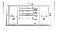
図1に、決定論的BIST構造を含むSOC100を示す。例えば、決定論的BIST構造は、パターンジェネレータ102とシグナチャアナライザ104を含む。パターンジェネレータ102とシグナチャアナライザ104の間には、複数のスキャンチェーン106、108、110、112が結合されている。使用する際、外部で生成されたスキャン「シード」(すなわち、ATE114によって提供されたシード)が、パターンジェネレータ102に提供される。次に、パターンジェネレータ102は、そのシードを複数のスキャンパターンを生成する基準として使用し、スキャンパターンは様々なスキャンチェーン106〜112内にシフトされる。スキャンチェーン106〜112からのパターンを開始した後で、パターンに対する応答がスキャンチェーン106〜112を介して捕捉され、シグナチャアナライザ104にシフトされる。決定論的BISTでは、シグナチャアナライザ104は、何十万ものシフトされたビットを128ビットシグナチャに変換することができる多入力シフトレジスタ(MISR)を含むことがある。
FIG. 1 shows an
決定論的BIST構造は、生産テストモードと診断テストモードを含むいくつかのモードで動作することができる。生産テストモードでは、SOCのスキャンチェーン106〜112が、図1に示したように、決定論的BISTパターンジェネレータ102とシグナチャアナライザ104の間に結合されている。診断テストモードでは、SOCのスキャンチェーン106〜112は、パターンジェネレータ102に結合されるが、シグナチャアナライザ104から切り離されている(すなわち、その出力がシグナチャアナライザ104をバイパスする)。したがって、診断テストモードでは、スキャンチェーン106〜112から生応答データを得ることができる。次に、この生応答データをSOC100の外部でより詳しく解析することができる。
The deterministic BIST structure can operate in several modes including a production test mode and a diagnostic test mode. In production test mode, SOC scan chains 106-112 are coupled between deterministic
一般に、決定論的BISTハードウェア102、104は、スキャンテストの「第1のパス」の間生産テストモードにされる。この第1のパスの間に、欠陥スキャン区間(failing scan interval)(すなわち、スキャンパターンのグループ)が識別される。第2のパスの間に、決定論的BISTハードウェア102、104が診断テストモードにされ、欠陥区間のスキャンパターンが再実行されることがある。
In general, the
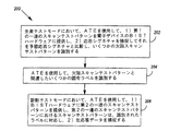
欠陥区間のスキャンパターンを再実行するために、テスト技術者は、一般に、設計技師から提供される情報を使用して欠陥区間の記憶場所を手作業で識別しなければならなかった。その場合、テスト技術者は、ベクトルデータを処理して欠陥区間を再実行しなければならず、またテスタメモリ制限を超えないようにしなければならなかった(すなわち、大量の生応答データがテスタメモリ制限を超えることがあるので)。これらのほとんど手作業の工程は、時間がかかり誤りが起きやすく、生産テストの際に大きな遅延と破壊を引き起こす可能性がある。したがって、図2は、図1に示したようなBISTハードウェアを有する電子デバイスにスキャンパターンを提供する新しい方法を示す。 In order to re-execute the scan pattern of the defective section, the test engineer typically had to manually identify the storage location of the defective section using information provided by the design engineer. In that case, the test engineer had to process the vector data to re-execute the defective interval and not to exceed the tester memory limit (i.e., a large amount of raw response data was stored in the tester memory). Because the limit may be exceeded). These almost manual processes are time consuming and error prone and can cause significant delays and destruction during production testing. Accordingly, FIG. 2 illustrates a new method for providing a scan pattern to an electronic device having BIST hardware as shown in FIG.
方法200は、次のように進行する。生産テストモードにおいて、自動テスト機器(ATE)を使用して、1)第1の一連のスキャンテストパターンを電子デバイスのBISTハードウェアに提供し、2)応答シグネチャを捕捉しそれを予想応答シグネチャと比較する202。次に、比較の結果を使用して、いくつかの欠陥スキャンテストパターンを識別することができる。次に、ATEを使用して、欠陥スキャンテストパターンと関連したいくつかの固有ラベルを識別する204。診断テストモードにおいて、ATEを使用して、1)BISTハードウェアに第2の一連のスキャンテストパターンを提供し、2)生応答データを捕捉する206。第2の一連のスキャンテストパターンにおけるスキャンテストパターンは、識別されたラベルに対応する。
方法200の1つの実施形態において、それぞれの一連のスキャンテストパターンは、スキャンテストパターンの複数の区間を含むことができる(例えば、Synopsis社のDBISTの場合のように)。次に、スキャンテストパターンのいくつかの欠陥区間に対応するラベルを識別することによって、いくつかの欠陥スキャンテストパターンを識別することができる。
In one embodiment of the
例えばそれぞれの様々なスキャンパターン(または、スキャンパターンの区間)を別々に記憶することによって、様々なスキャンパターンまたは様々なスキャンパターンの様々な区間と固有のラベルを関連付けることができる。このようにして、BISTハードウェアが生産テストモードか診断テストモードかに関係なく、スキャンパターンの様々なベクトルを同じテストパターンからコンパイルすることができる。各区間ごとにラベルを提供するだけでよいが、ラベルをさらに細かく細分することにより(すなわち、各スキャンパターンごとのラベル)、生産テストの時間とメモリをより効率的に使用することができる。 For example, by storing each different scan pattern (or section of scan pattern) separately, a unique label can be associated with different scan patterns or different sections of different scan patterns. In this way, different vectors of scan patterns can be compiled from the same test pattern regardless of whether the BIST hardware is in production test mode or diagnostic test mode. It is only necessary to provide a label for each section, but by subdividing the labels (ie, labels for each scan pattern), production test time and memory can be used more efficiently.
場合によっては、生産テストモードの際に電子デバイスに提供される一連のスキャンテストパターンは、単一の生産テストベクトル内で実行されることがある(例えば、「バースト」モードで)。この場合、診断テストモードにおいて、ATEは、複数の診断テストベクトルを動的に生成し実行することもあり(例えば、「アンバースト(unburst)」モードでは各識別ラベルごとのベクトル、またはATEのメモリ制限内に収まる生応答データが作成されるラベルのグループのベクトル)、あるいは、ATEは、識別したラベルを単一の診断テストベクトルに動的にコンパイルすることもある(例えば、「バースト」モードで)。 In some cases, a series of scan test patterns provided to an electronic device during a production test mode may be performed within a single production test vector (eg, in “burst” mode). In this case, in the diagnostic test mode, the ATE may dynamically generate and execute a plurality of diagnostic test vectors (for example, in the “unburst” mode, a vector for each identification label or a memory of the ATE). Or a vector of groups of labels from which raw response data is generated that falls within limits), or the ATE may dynamically compile the identified labels into a single diagnostic test vector (eg, in “burst” mode). ).
例えば、方法200によって使用されるATEは、Agilent Technologies, Inc.(カリフォルニア州パロアルト)から提供されている93000SOCテスタなどのシステムオンチップ(SOC)テスタでよい。しかしながら、93000SOCテスタが、データを並列に複数の装置ピンに提供し複数の装置ピンから収集できる場合は、方法300の方が93000SOCテスタの機能を利用するのに適している場合がある。
For example, the ATE used by the
方法300は、以下のように動作する。ATEを使用して、生産テストモードにおいて、1)電子デバイスの複数の入力ピンに一連のスキャンテストパターンを提供し、2)電子デバイスの出力ピンにおいて応答シグネチャを捕捉する302。次に、捕捉した応答シグネチャを予想応答シグネチャと比較して、各入力ピンに対応するいくつかの欠陥スキャンテストパターンを識別する。次に、ATEを使用して、欠陥スキャンテストパターンと関連付けられたいくつかの固有ラベルを識別する304。診断テストモードでは、各入力ピンごとに、ATEを使用して、1)第2の一連のスキャンテストパターンを入力ピンに提供し、2)生応答データを捕捉する306。第2の一連のテストパターンのスキャンテストパターンは、入力ピンの識別されたラベルに対応する。
The
方法300の1つの実施形態において、それぞれの一連のスキャンテストパターンは、スキャンテストパターンの複数の区間を含むことができる(例えば、Synopsis社のDBISTのような)。次に、スキャンテストパターンの欠陥区間に対応するいくつかのラベルを識別することによって、いくつかの欠陥スキャンテストパターンを識別することができる。
In one embodiment of the
いくつかの場合は、生産テストモードの間に入力ピンに提供される一連のスキャンテストパターンが、単一の生産テストベクトル内で実行されることがある。他の場合は、電子デバイスの入力ピンに提供される一連のすべてのスキャンテストパターンが単一の生産テストベクトル内で実行されることがある。 In some cases, a series of scan test patterns provided on input pins during production test mode may be performed within a single production test vector. In other cases, a series of all scan test patterns provided at the input pins of the electronic device may be performed within a single production test vector.
診断テストモードが終わると、ATEは、装置の各入力ピンごとに複数の診断テストベクトルを動的に生成し実行することができる。例えば、ATEは、識別されたラベルごとのベクトルを実行したり、ATEのメモリ制限内に収まる生応答データが作成されるラベルのグループのベクトルを実行したりすることができる。代替として、ATEは、識別したラベルを、各ピンごとの単一の診断テストベクトルまたは装置の単一の診断テストベクトルに動的にコンパイルすることができる。 Upon completion of the diagnostic test mode, the ATE can dynamically generate and execute multiple diagnostic test vectors for each input pin of the device. For example, the ATE can execute a vector for each identified label or a vector of groups of labels from which raw response data that falls within the memory limits of the ATE is created. Alternatively, the ATE can dynamically compile the identified labels into a single diagnostic test vector for each pin or a single diagnostic test vector for the device.
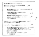
方法200、300はいずれも、その変形を含み、(固定式か取り外し式かに関係なく)メモリやディスクなどのコンピュータ可読媒体400に記憶されたプログラムコード402〜414で実施することができる。本明細書において、「メモリ」は、統合メモリ構造あるいは分散型または機能固有のメモリ構造を両方とも対象として含むように解釈されることに注意されたい。例えば、93000SOCテスタは、93000SOCテスタの各ピンごとのベクトルとシーケンサ(すなわち、プログラム命令)をそれぞれ記憶するために、ピンごとのベクトルとシーケンサメモリに分割されたメモリ構造を含む。
Both
方法200の場合、プログラムコードは、ATEに電子デバイスのBISTハードウェアを生産テストモードにさせる402プログラムコードを含むことができる。次に、BISTハードウェアが生産テストモードの間、プログラムコードは、ATEに、1)第1の一連のスキャンテストパターンを前記BISTハードウェアに提供させ404、2)スキャンテストパターンに対応する応答シグネチャを捕捉させ406、3)捕捉応答シグネチャを予想応答シグネチャと比較させていくつかの欠陥スキャンテストパターンを識別させる408。次に、プログラムコードは、欠陥スキャンテストパターンと関連付けられたいくつかの固有ラベルを識別することができる410。その後、プログラムコードは、ATEに装置のBISTハードウェアを診断テストモードにさせることができる412。BISTハードウェアが診断テストモードの間、プログラムコードは、ATEに、1)第2の一連のスキャンテストパターンをBISTハードウェアに提供させ414、2)スキャンテストパターンに対応する生応答データを捕捉させる416ことができる。前に述べたように、第2の一連のスキャンテストパターンにおけるスキャンテストパターンは、欠陥スキャンテストパターンと関連付けられたラベルによって識別されるものに対応することができる。
For
方法200の他の特徴および変形、ならびに方法300の特徴および変形は、同じようにプログラムコードで実施することができる。
Other features and variations of
100 SOC
102 パターンジェネレータ
104 シグナチャアナライザ
106、108、110、112 スキャンチェーン
114 ATE
100 SOC
102 Pattern Generator 104
Claims (10)
生産テストモードにおいて、自動テスト機器を使用して、i)第1の一連のスキャンテストパターンを前記自己テストハードウェアに提供し、ii)応答シグネチャを捕捉し予想応答シグネチャと比較して、いくつかの欠陥スキャンテストパターンを識別するステップと、
前記自動テスト機器を使用して、前記欠陥スキャンテストパターンと関連したいくつかの固有ラベルを識別すると、
診断テストモードにおいて、前記自動テスト機器を使用して、i)第2の一連のスキャンテストパターンを前記自己テスハードウェアに提供し、前記第2の一連のスキャンテストパターンにおけるスキャンテストパターンが前記識別されたラベルに対応し、ii)生応答データを捕捉するステップと、
を含むことを特徴とする方法。 A method for providing a scan pattern to an electronic device having embedded self-test hardware, the self-test hardware having a production test mode and a diagnostic test mode, wherein the electronic device is one in the production test mode. Or output a plurality of response signatures, output raw response data in the diagnostic test mode,
In production test mode, using automated test equipment, i) providing a first series of scan test patterns to the self-test hardware, ii) capturing response signatures and comparing them with expected response signatures, Identifying a defect scan test pattern of
Using the automated test equipment to identify a number of unique labels associated with the defect scan test pattern;
In diagnostic test mode, using the automatic test equipment, i) providing a second series of scan test patterns to the self-test hardware, wherein the scan test patterns in the second series of scan test patterns are identified. Ii) capturing raw response data;
A method comprising the steps of:
前記コンピュータ可読媒体に記憶され、自動テスト機器に、
電子デバイスの組み込み自己テストハードウェアを生産テストモードにする動作、
第1の一連のスキャンテストパターンを前記自己テストハードウェアに提供する動作、
前記スキャンテストパターンに対応する応答シグネチャを捕捉する動作、
前記捕捉した応答シグネチャを予想応答シグネチャと比較して、いくつかの欠陥スキャンテストパターンを識別する動作、
前記欠陥スキャンテストパターンと関連した固有ラベルの数を識別する動作、
前記自己テストハードウェアを診断テストモードにする動作、
前記自己テストハードウェアに第2の一連のスキャンテストパターンを提供する動作であって、前記第2の一連のスキャンテストパターンにおける前記スキャンテストパターンが前記識別したラベルに対応する動作、および、
前記スキャンテストパターンに対応する生応答データを捕捉する動作、
を実行させるプログラムコードと、
を有することを特徴とする装置。 A computer readable medium;
Stored in the computer-readable medium,
The operation of the electronic device's built-in self-test hardware into production test mode,
Providing a first series of scan test patterns to the self-test hardware;
Capturing a response signature corresponding to the scan test pattern;
Comparing the captured response signature with an expected response signature to identify a number of defect scan test patterns;
Identifying the number of unique labels associated with the defect scan test pattern;
An operation to put the self-test hardware into a diagnostic test mode;
Providing a second series of scan test patterns to the self-test hardware, wherein the scan test patterns in the second series of scan test patterns correspond to the identified labels; and
Capturing raw response data corresponding to the scan test pattern;
Program code to execute
A device characterized by comprising:
When the scan test pattern in the second series of scan test patterns is provided to the self-test hardware, the program code causes the automatic test equipment to dynamically generate and execute a plurality of diagnostic test vectors. The apparatus according to claim 6.
Applications Claiming Priority (1)
| Application Number | Priority Date | Filing Date | Title |
|---|---|---|---|
| US10/959,856 US7254760B2 (en) | 2004-10-05 | 2004-10-05 | Methods and apparatus for providing scan patterns to an electronic device |
Publications (2)
| Publication Number | Publication Date |
|---|---|
| JP2006105997A true JP2006105997A (en) | 2006-04-20 |
| JP2006105997A5 JP2006105997A5 (en) | 2008-11-13 |
Family
ID=36120724
Family Applications (1)
| Application Number | Title | Priority Date | Filing Date |
|---|---|---|---|
| JP2005292299A Pending JP2006105997A (en) | 2004-10-05 | 2005-10-05 | Method and device for providing scanning pattern to electronic device |
Country Status (4)
| Country | Link |
|---|---|
| US (1) | US7254760B2 (en) |
| JP (1) | JP2006105997A (en) |
| DE (1) | DE102005026403B4 (en) |
| TW (1) | TWI370261B (en) |
Families Citing this family (9)
| Publication number | Priority date | Publication date | Assignee | Title |
|---|---|---|---|---|
| US7685487B1 (en) * | 2005-03-22 | 2010-03-23 | Advanced Micro Devices, Inc. | Simultaneous core testing in multi-core integrated circuits |
| US7526694B1 (en) * | 2006-08-03 | 2009-04-28 | Xilinx, Inc. | Integrated circuit internal test circuit and method of testing therewith |
| US20080077835A1 (en) * | 2006-09-27 | 2008-03-27 | Khoche A Jay | Automatic Test Equipment Receiving Diagnostic Information from Devices with Built-in Self Test |
| US7650547B2 (en) | 2007-02-28 | 2010-01-19 | Verigy (Singapore) Pte. Ltd. | Apparatus for locating a defect in a scan chain while testing digital logic |
| US8127186B2 (en) | 2007-02-28 | 2012-02-28 | Verigy (Singapore) Pte. Ltd. | Methods and apparatus for estimating a position of a stuck-at defect in a scan chain of a device under test |
| US20080235545A1 (en) * | 2007-03-06 | 2008-09-25 | Vinay Burjinroppa Jayaram | Re-using production test scan paths for system test of an integrated circuit |
| US9183105B2 (en) * | 2013-02-04 | 2015-11-10 | Alcatel Lucent | Systems and methods for dynamic scan scheduling |
| CN108508352B (en) * | 2018-04-19 | 2020-11-24 | 中国电子科技集团公司第五十八研究所 | Test code generating circuit |
| US11156660B1 (en) * | 2019-12-19 | 2021-10-26 | Cadence Design Systems, Inc. | In-system scan test of electronic devices |
Citations (1)
| Publication number | Priority date | Publication date | Assignee | Title |
|---|---|---|---|---|
| JPH11202026A (en) * | 1998-01-13 | 1999-07-30 | Hitachi Ltd | Method for failure analysis |
Family Cites Families (8)
| Publication number | Priority date | Publication date | Assignee | Title |
|---|---|---|---|---|
| US5790562A (en) * | 1996-05-06 | 1998-08-04 | General Motors Corporation | Circuit with built-in test and method thereof |
| US6393594B1 (en) * | 1999-08-11 | 2002-05-21 | International Business Machines Corporation | Method and system for performing pseudo-random testing of an integrated circuit |
| US6591211B1 (en) * | 1999-08-27 | 2003-07-08 | Intel Corporation | Testing unit and self-evaluating device |
| US6557129B1 (en) | 1999-11-23 | 2003-04-29 | Janusz Rajski | Method and apparatus for selectively compacting test responses |
| US6424926B1 (en) * | 2000-03-31 | 2002-07-23 | Intel Corporation | Bus signature analyzer and behavioral functional test method |
| DE10122619C1 (en) * | 2001-05-10 | 2003-02-13 | Infineon Technologies Ag | Test circuit for testing a synchronous circuit |
| US7159145B2 (en) * | 2003-05-12 | 2007-01-02 | Infineon Technologies Ag | Built-in self test system and method |
| US7321999B2 (en) * | 2004-10-05 | 2008-01-22 | Verigy (Singapore) Pte. Ltd. | Methods and apparatus for programming and operating automated test equipment |
-
2004
- 2004-10-05 US US10/959,856 patent/US7254760B2/en active Active
-
2005
- 2005-04-14 TW TW094111829A patent/TWI370261B/en active
- 2005-06-08 DE DE102005026403A patent/DE102005026403B4/en not_active Expired - Fee Related
- 2005-10-05 JP JP2005292299A patent/JP2006105997A/en active Pending
Patent Citations (1)
| Publication number | Priority date | Publication date | Assignee | Title |
|---|---|---|---|---|
| JPH11202026A (en) * | 1998-01-13 | 1999-07-30 | Hitachi Ltd | Method for failure analysis |
Also Published As
| Publication number | Publication date |
|---|---|
| US20060075316A1 (en) | 2006-04-06 |
| US7254760B2 (en) | 2007-08-07 |
| TW200612239A (en) | 2006-04-16 |
| TWI370261B (en) | 2012-08-11 |
| DE102005026403B4 (en) | 2007-12-13 |
| DE102005026403A1 (en) | 2006-04-20 |
Similar Documents
| Publication | Publication Date | Title |
|---|---|---|
| US7908532B2 (en) | Automated system and processing for expedient diagnosis of broken shift registers latch chains | |
| US7774662B2 (en) | Method and structure for picosecond-imaging-circuit-analysis based built-in-self-test diagnostic | |
| JP2006105997A (en) | Method and device for providing scanning pattern to electronic device | |
| US8522097B2 (en) | Logic built-in self-test programmable pattern bit mask | |
| US7475308B2 (en) | implementing deterministic based broken scan chain diagnostics | |
| US20090089636A1 (en) | Method and Apparatus for Logic Built In Self Test (LBIST) Fault Detection in Multi-Core Processors | |
| US7702980B2 (en) | Scan-load-based dynamic scan configuration | |
| US20030131294A1 (en) | Stuck-at fault scan chain diagnostic method | |
| US10509072B2 (en) | Test application time reduction using capture-per-cycle test points | |
| US20090217116A1 (en) | Diagnosable general purpose test registers scan chain design | |
| TWI781634B (en) | An automated test equipment, a process and a computer program for testing one or more devices under test, wherein different test activities make use of subsets of the device under test resources | |
| US7921346B2 (en) | Verification of array built-in self-test (ABIST) design-for-test/design-for-diagnostics (DFT/DFD) | |
| US6557132B2 (en) | Method and system for determining common failure modes for integrated circuits | |
| US11815555B2 (en) | Universal compactor architecture for testing circuits | |
| US7607057B2 (en) | Test wrapper including integrated scan chain for testing embedded hard macro in an integrated circuit chip | |
| US8423845B2 (en) | On-chip logic to log failures during production testing and enable debugging for failure diagnosis | |
| US10963612B2 (en) | Scan cell architecture for improving test coverage and reducing test application time | |
| US6314540B1 (en) | Partitioned pseudo-random logic test for improved manufacturability of semiconductor chips | |
| JP2006105996A (en) | Method and device for programming and operating automatic testing equipment | |
| US20180238962A1 (en) | Structurally assisted functional test and diagnostics for integrated circuits | |
| US20090210761A1 (en) | AC Scan Diagnostic Method and Apparatus Utilizing Functional Architecture Verification Patterns | |
| US6865704B2 (en) | Scan multiplexing for increasing the effective scan data exchange rate | |
| Cook et al. | Diagnosis of multiple faults with highly compacted test responses | |
| US11092645B2 (en) | Chain testing and diagnosis using two-dimensional scan architecture | |
| US10613142B2 (en) | Non-destructive recirculation test support for integrated circuits |
Legal Events
| Date | Code | Title | Description |
|---|---|---|---|
| A711 | Notification of change in applicant |
Free format text: JAPANESE INTERMEDIATE CODE: A711 Effective date: 20071025 |
|
| RD03 | Notification of appointment of power of attorney |
Free format text: JAPANESE INTERMEDIATE CODE: A7423 Effective date: 20080201 |
|
| A521 | Request for written amendment filed |
Free format text: JAPANESE INTERMEDIATE CODE: A523 Effective date: 20080929 |
|
| A621 | Written request for application examination |
Free format text: JAPANESE INTERMEDIATE CODE: A621 Effective date: 20080929 |
|
| A131 | Notification of reasons for refusal |
Free format text: JAPANESE INTERMEDIATE CODE: A131 Effective date: 20110819 |
|
| A02 | Decision of refusal |
Free format text: JAPANESE INTERMEDIATE CODE: A02 Effective date: 20120131 |