JP2006073618A - Optical element and manufacturing method thereof - Google Patents

Optical element and manufacturing method thereof Download PDF

Info

Publication number
JP2006073618A
JP2006073618A JP2004252499A JP2004252499A JP2006073618A JP 2006073618 A JP2006073618 A JP 2006073618A JP 2004252499 A JP2004252499 A JP 2004252499A JP 2004252499 A JP2004252499 A JP 2004252499A JP 2006073618 A JP2006073618 A JP 2006073618A
Authority
JP
Japan
Prior art keywords
layer
electrode
semiconductor layer
led element
external electrode
Prior art date
Legal status (The legal status is an assumption and is not a legal conclusion. Google has not performed a legal analysis and makes no representation as to the accuracy of the status listed.)
Withdrawn
Application number
JP2004252499A
Other languages
Japanese (ja)
Other versions
JP2006073618A5 (en
Inventor
Satoshi Wada
聡 和田
Current Assignee (The listed assignees may be inaccurate. Google has not performed a legal analysis and makes no representation or warranty as to the accuracy of the list.)
Toyoda Gosei Co Ltd
Original Assignee
Toyoda Gosei Co Ltd
Priority date (The priority date is an assumption and is not a legal conclusion. Google has not performed a legal analysis and makes no representation as to the accuracy of the date listed.)
Filing date
Publication date
Application filed by Toyoda Gosei Co Ltd filed Critical Toyoda Gosei Co Ltd
Priority to JP2004252499A priority Critical patent/JP2006073618A/en
Priority to US11/157,174 priority patent/US20060001035A1/en
Publication of JP2006073618A publication Critical patent/JP2006073618A/en
Publication of JP2006073618A5 publication Critical patent/JP2006073618A5/ja
Withdrawn legal-status Critical Current

Links

Images

Landscapes

  • Led Device Packages (AREA)
  • Led Devices (AREA)

Abstract

<P>PROBLEM TO BE SOLVED: To provide an optical element along with its manufacturing method in which an illumination area that occupies the entire element is larger, with excellent mounting characteristics, reliability in electrical connection, and heat radiation characteristics, while using an existing facility and known manufacturing method, with no advanced processing technology required. <P>SOLUTION: Based on a manufacturing process for a semiconductor light emitting element with a wafer-like sapphire substrate 10, an LED element 1 is formed where an n external electrode 17 and p external electrode 18 are provided around a light emitting layer 13. Thus, using an existing facility and a known manufacturing method, an LED element 1 is easily mass-produced in a lump. <P>COPYRIGHT: (C)2006,JPO&NCIPI

Description

本発明は光学素子に関し、特に、高度な加工技術を要することなく、既存の設備および既知の製造方法を使用しながら素子全体に占める発光面積を大にでき、実装性に優れ、電気的接続の信頼性が大で、良好な放熱性を有する光学素子およびその製造方法に関する。   The present invention relates to an optical element, and in particular, without requiring advanced processing technology, the light emitting area occupying the entire element can be increased while using existing equipment and a known manufacturing method, and is excellent in mountability and electrical connection. The present invention relates to an optical element having high reliability and good heat dissipation and a method for manufacturing the same.

従来の光学素子として、サファイア等の光透過性の下地基板上にIII族窒化物系化合物半導体等の半導体結晶を成長させたLED素子(Light Emitting Diode:以下、LED素子という。)が知られている。LED素子は、n型およびp型の窒化物系化合物半導体層(以下、半導体層という)に通電することによって発光層内で発光し、発光に基づく光を外部放射する。   As a conventional optical element, an LED element (Light Emitting Diode: hereinafter referred to as an LED element) in which a semiconductor crystal such as a group III nitride compound semiconductor is grown on a light-transmitting base substrate such as sapphire is known. Yes. The LED element emits light in the light emitting layer by energizing n-type and p-type nitride compound semiconductor layers (hereinafter referred to as semiconductor layers), and emits light based on the light emission to the outside.

LED素子のn型およびp型の半導体層に通電するにあたって、LED素子最上層のp型半導体層に通電する第1の電極を設け、更に、p型半導体層からエッチングを施すことにより露出させたn型半導体層に第2の電極を設けて、ワイヤボンディングによって外部回路との電気的接続を行うことが知られている。このようなLED素子では、光取り出し面に第1の電極が設けられるためにLED素子から出射される光の取り出しが妨げられるという不都合がある。   When energizing the n-type and p-type semiconductor layers of the LED element, a first electrode for energizing the p-type semiconductor layer, which is the uppermost layer of the LED element, is provided and further exposed by etching from the p-type semiconductor layer. It is known that a second electrode is provided on an n-type semiconductor layer and is electrically connected to an external circuit by wire bonding. In such an LED element, since the first electrode is provided on the light extraction surface, extraction of light emitted from the LED element is hindered.

一方、外部回路との電気的接続をワイヤによらずにAu等のパンプを介してフリップチップ接合し、発光層での発光に基づく光をサファイア基板側から取り出すようにしたLED素子が提案されている。このようなLED素子では、短絡を生じることなく、かつバンプ接合に必要な面積の第1および第2の電極を設ける必要があり、そのことによって素子全体に占める発光面積を大にすることが難しいという不都合がある。   On the other hand, an LED element has been proposed in which electrical connection with an external circuit is flip-chip bonded via a pump such as Au without using a wire, and light based on light emission in the light emitting layer is extracted from the sapphire substrate side. Yes. In such an LED element, it is necessary to provide the first and second electrodes having an area necessary for bump bonding without causing a short circuit, and thus it is difficult to increase the light emitting area in the entire element. There is an inconvenience.

かかる問題を解消するものとして、LED素子のn型半導体層およびp型半導体層に電圧印加を行うための電極を側面部に設けたLED素子が提案されている(例えば、特許文献1参照。)。   In order to solve such a problem, an LED element in which an electrode for applying a voltage to the n-type semiconductor layer and the p-type semiconductor layer of the LED element is provided on the side surface has been proposed (for example, see Patent Document 1). .

特許文献1に記載されるLED素子は、特許文献1の図1に示されているように、積層部の両側面部およびサファイア基板の両側面部に、たとえば酸化シリコン(SiO2)製の絶縁層を形成されている。一方の絶縁層は、積層部の最表面に位置するp型GaN層の端面部と接触する箇所にエッチングが施されている。また他方の絶縁膜は、n型GaN層の端面部と接触する箇所にエッチングが施されており、エッチングの部位を介してp型GaN層およびn型GaN層に導通する導電性膜からなる電極が絶縁層の外表面に設けられている。 As shown in FIG. 1 of Patent Document 1, the LED element described in Patent Document 1 includes insulating layers made of, for example, silicon oxide (SiO 2 ) on both side surfaces of the laminated portion and both side surfaces of the sapphire substrate. Is formed. One insulating layer is etched at a location in contact with the end face portion of the p-type GaN layer located on the outermost surface of the stacked portion. In addition, the other insulating film is etched at a location where it comes into contact with the end face portion of the n-type GaN layer, and an electrode made of a conductive film that conducts to the p-type GaN layer and the n-type GaN layer via the etched portion. Is provided on the outer surface of the insulating layer.

特許文献1に記載されるLED素子によれば、半導体発光素子の積層部の表面部に電極は形成されていないため、発光層から発せられる光は効率よく上方向へ出射することとなる。また、発光層がエッチングによってその面積が減じられているようなこともなく、発光層の発光面積としては、サファイア基板と同一の大きな面積に形成しておくことができる。したがって、積層部の最表面の部位から上向きに出射される光量を大きくでき、発光強度を高めることができるとしている。
特開平8−102552号公報(〔0024〕〜〔0032〕、図1〕
According to the LED element described in Patent Document 1, since the electrode is not formed on the surface portion of the laminated portion of the semiconductor light emitting element, the light emitted from the light emitting layer is efficiently emitted upward. Moreover, the area of the light emitting layer is not reduced by etching, and the light emitting area of the light emitting layer can be formed in the same large area as the sapphire substrate. Therefore, the amount of light emitted upward from the outermost surface portion of the laminated portion can be increased, and the light emission intensity can be increased.
JP-A-8-102552 ([0024] to [0032], FIG. 1)

しかし、特許文献1に記載されるLED素子によると、サファイア基板に積層部を形成し、これをダイシングしてチップに分割した後に絶縁層に対してエッチングを行い、エッチング部位を介してp型GaN層およびn型GaN層に導通する電極を設けているため、個々のチップに対する微細かつ高度な加工技術を要し、一括多量生産が難しいという問題がある。また、電気的接続性の向上が図られても、発光に伴って生じる熱に対して充分な放熱性が得られなければ発光効率は向上せず、高輝度化、大出力化を実現することができない。   However, according to the LED element described in Patent Document 1, a laminated portion is formed on a sapphire substrate, and this is diced and divided into chips, and then the insulating layer is etched, and p-type GaN is passed through the etched portion. Since the electrode which conducts to the layer and the n-type GaN layer is provided, there is a problem that it is difficult to perform mass mass production because it requires fine and advanced processing technology for each chip. Also, even if the electrical connectivity is improved, if sufficient heat dissipation is not obtained for the heat generated by light emission, the light emission efficiency will not improve, and high brightness and high output will be realized. I can't.

従って、本発明の目的は、高度な加工技術を要することなく、既存の設備および既知の製造方法を使用しながら素子全体に占める発光面積を大にでき、実装性に優れ、電気的接続の信頼性が大で、良好な放熱性を有する光学素子およびその製造方法を提供することにある。   Therefore, the object of the present invention is to increase the light emitting area in the entire device using existing equipment and a known manufacturing method without requiring advanced processing technology, and is excellent in mountability and reliability of electrical connection. It is an object of the present invention to provide an optical element having a high performance and a good heat dissipation property and a method for manufacturing the same.

本発明は、上記の目的を達成するため、発光層を含む半導体層と、素子全幅より小なる幅を有する前記半導体層の周縁に設けられ、前記発光層に給電するn側およびp側の電極とを有することを特徴とする光学素子を提供する。   In order to achieve the above object, the present invention provides a semiconductor layer including a light emitting layer and n-side and p-side electrodes provided on the periphery of the semiconductor layer having a width smaller than the entire width of the element and supplying power to the light emitting layer. The optical element characterized by having these.

また、本発明は、上記の目的を達成するため、ウエハー状の下地基板に半導体材料を積層して発光層を含む半導体層を形成する半導体層形成工程と、前記半導体層の表面から所定の幅および深さを有するように前記半導体層を除去して露出部を形成する半導体層除去工程と、前記露出部に前記半導体層のn層およびp層へ給電する電極を形成する電極形成工程と、前記電極が素子周縁に露出するように前記下地基板および前記半導体層を切断して素子化する素子化工程とを含むことを特徴とする光学素子の製造方法を提供する。   In order to achieve the above object, the present invention provides a semiconductor layer forming step of forming a semiconductor layer including a light emitting layer by laminating a semiconductor material on a wafer-like base substrate, and a predetermined width from the surface of the semiconductor layer. And a semiconductor layer removing step of removing the semiconductor layer so as to have a depth to form an exposed portion, and an electrode forming step of forming electrodes for supplying power to the n layer and the p layer of the semiconductor layer in the exposed portion, There is provided an optical element manufacturing method including an element forming step of cutting the base substrate and the semiconductor layer into an element so that the electrode is exposed at the periphery of the element.

本発明によれば、素子全体に占める発光面積を大にでき、高度かつ高価な設備を要することなく実装性に優れ、電気的接続の信頼性が大で、サイズが大であっても良好な放熱性を付与することができる。   According to the present invention, the light emitting area occupying the entire element can be increased, and it is excellent in mountability without requiring sophisticated and expensive equipment, the reliability of electrical connection is large, and even if the size is large, it is good. Heat dissipation can be imparted.

(第1の実施の形態)
(LED素子1の構成)
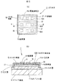
図1は、第1の実施の形態に係るLED素子を示し、(a)は素子対角線方向に切断した縦断面図、(b)はLED素子の光取り出し面側から見た平面図である。
(First embodiment)
(Configuration of LED element 1)
1A and 1B show an LED element according to a first embodiment, in which FIG. 1A is a longitudinal sectional view cut in a diagonal direction of the element, and FIG. 1B is a plan view seen from the light extraction surface side of the LED element.

このLED素子1は、図1(a)に示すように、サファイア基板10上にIII族窒化物系化合物半導体を結晶成長させたものであり、サファイア基板10上にAlNバッファ層11と、III族窒化物系化合物半導体層によって構成されるn−GaN層12と、発光層13と、p−GaN層14と、p−GaN層14に電流を拡散させるpコンタクト電極15とを順次積層し、GaN系半導体層100の側面に光透過性を有する絶縁層16と、p−GaN層14からn−GaN層12にかけてエッチングで除去することにより露出したn−GaN層12に設けられるn外部電極17と、サファイア基板10上のAlNバッファ層11からpコンタクト電極15にかけてのGaN系半導体層100の側面に設けられるp外部電極18と、n外部電極17からp外部電極18にかけての素子表面を覆う光透過性を有する絶縁層19とを有する。   As shown in FIG. 1A, the LED element 1 is obtained by growing a group III nitride compound semiconductor on a sapphire substrate 10 and includes an AlN buffer layer 11 and a group III on the sapphire substrate 10. An n-GaN layer 12 composed of a nitride compound semiconductor layer, a light emitting layer 13, a p-GaN layer 14, and a p-contact electrode 15 for diffusing current in the p-GaN layer 14 are sequentially stacked, and GaN An insulating layer 16 having optical transparency on the side surface of the semiconductor layer 100, an n external electrode 17 provided on the n-GaN layer 12 exposed by etching from the p-GaN layer 14 to the n-GaN layer 12, and The p external electrode 18 provided on the side surface of the GaN-based semiconductor layer 100 from the AlN buffer layer 11 to the p contact electrode 15 on the sapphire substrate 10, and the n external electrode 1 And an insulating layer 19 having light transmittance that covers the element surface of the over the p external electrodes 18 from.

以下の説明においては、サファイア基板10上のAlNバッファ層11から絶縁層19にかけての部分をGaN系半導体層100としている。このLED素子1の発光層13から放射される光の発光波長は460nmである。   In the following description, the portion from the AlN buffer layer 11 to the insulating layer 19 on the sapphire substrate 10 is a GaN-based semiconductor layer 100. The emission wavelength of light emitted from the light emitting layer 13 of the LED element 1 is 460 nm.

III族窒化物系化合物半導体層の形成方法は、特に限定されないが、周知の有機金属気相成長法(MOCVD法)、分子線結晶成長法(MBE法)、ハライド系気相成長法(HVPE法)、スパッタ法、イオンプレーティング法、電子シャワー法等によって形成することができる。なお、LED素子の構成としては、ホモ構造、ヘテロ構造若しくはダブルへテロ構造のものを用いることができる。さらに、量子井戸構造(単一量子井戸構造若しくは多重量子井戸構造)を採用することもできる。   The formation method of the group III nitride compound semiconductor layer is not particularly limited, but the well-known metal organic chemical vapor deposition method (MOCVD method), molecular beam crystal growth method (MBE method), halide vapor phase epitaxy method (HVPE method). ), A sputtering method, an ion plating method, an electron shower method, or the like. In addition, as a structure of a LED element, the thing of a homo structure, a hetero structure, or a double hetero structure can be used. Furthermore, a quantum well structure (single quantum well structure or multiple quantum well structure) can also be adopted.

pコンタクト電極15は、p−GaN層14に電流を拡散させるとともに、外部との良好な電気的接続性を付与するためのものであり、本実施の形態では光反射性を有するRhによって形成されている。なお、pコンタクト電極15は、p−GaN層14とオーミック接触可能な材料であれば光透過性を有するITO(Indium Tin Oxide)、ZnO、Au/Co、Ni/Ti等の透光性材料で形成されても良い。   The p-contact electrode 15 is for diffusing current to the p-GaN layer 14 and providing good electrical connectivity with the outside. In this embodiment, the p-contact electrode 15 is formed of Rh having light reflectivity. ing. Note that the p-contact electrode 15 is made of a light-transmitting material such as ITO (Indium Tin Oxide), ZnO, Au / Co, or Ni / Ti that has optical transparency as long as the material can make ohmic contact with the p-GaN layer 14. It may be formed.

絶縁層16は、SiOからなり、GaN系半導体層の側面を覆うように設けられてn外部電極17およびp外部電極18がGaN系半導体層100と短絡することを防止する。なお、SiOに代えてSiN等の他の絶縁性材料を用いることもできる。 The insulating layer 16 is made of SiO 2 and is provided so as to cover the side surface of the GaN-based semiconductor layer, thereby preventing the n external electrode 17 and the p external electrode 18 from being short-circuited with the GaN-based semiconductor layer 100. It should be noted that other insulating materials such as SiN can be used instead of SiO 2 .

n外部電極17はV/Alからなり、p外部電極18はTiによって形成されている。これらの外部電極は、素子側面での電気的接合およびpコンタクト電極15側での面実装を可能とするために素子側面からpコンタクト電極15形成面にかけての素子周縁に露出するように形成されている。ここでいう素子周縁とは、例えば、図1に示すLED素子1の側面、および絶縁層19の設けられるGaN系半導体層100表面の縁である。その形成長は、n外部電極17が隣接する2辺の側面全体、p外部電極18はn外部電極17が形成される2辺に対向する2辺の一部に設けられており、p外部電極18の形成領域はn外部電極17より小となるように設けられる。なお、表面に半田メッキを施しても良い。   The n external electrode 17 is made of V / Al, and the p external electrode 18 is made of Ti. These external electrodes are formed so as to be exposed at the periphery of the element from the element side surface to the p contact electrode 15 formation surface in order to enable electrical bonding on the element side surface and surface mounting on the p contact electrode 15 side. Yes. The element periphery here is, for example, the side surface of the LED element 1 shown in FIG. 1 and the edge of the surface of the GaN-based semiconductor layer 100 on which the insulating layer 19 is provided. The formation length is provided on the entire side surface of two sides adjacent to the n external electrode 17, and the p external electrode 18 is provided on a part of the two sides opposite to the two sides on which the n external electrode 17 is formed. The region where 18 is formed is provided to be smaller than the n external electrode 17. The surface may be solder plated.

(LED素子1の製造工程)
図2(a)から(d)は、第1の実施の形態に係るLED素子の製造工程(LED素子の側面に絶縁層16を設ける工程まで)を示す図である。なお、以下の説明では、ウエハー状のサファイア基板10に対して半導体層を形成し、これを切り離して素子化する製造工程について説明を容易にするために、LED素子1となる部分を中心に示している。
(Manufacturing process of LED element 1)
FIGS. 2A to 2D are diagrams showing the LED element manufacturing process (up to the process of providing the insulating layer 16 on the side surface of the LED element) according to the first embodiment. In the following description, a semiconductor layer is formed on the wafer-like sapphire substrate 10 and a manufacturing process for separating the element into an element is illustrated, with the focus on the portion that becomes the LED element 1. ing.

(GaN系半導体層形成工程)
まず、図2(a)に示すように、結晶成長の下地基板となるウエハー状のサファイア基板10上にMOCVD法によってAlNバッファ層11、GaN系半導体層100、およびpコンタクト電極15を形成する。
(GaN-based semiconductor layer formation process)
First, as shown in FIG. 2A, an AlN buffer layer 11, a GaN-based semiconductor layer 100, and a p-contact electrode 15 are formed on a wafer-like sapphire substrate 10 serving as a base substrate for crystal growth by MOCVD.

(第1のエッチング工程)
次に、図2(b)に示すように、GaN系半導体層100に対してドライエッチングを行い、n外部電極およびp外部電極を設ける領域についてGaN系半導体層100の表面からn−GaN層12にかけて半導体層をその積層方向に除去することにより、GaN系半導体層100の側面に露出部12Aを設ける。なお、pコンタクト電極15は、露出部12Aに形成後にフォトレジストを施してpコンタクト電極15を形成し、その後フォトレジストを除去することによって形成するようにしても良い。
(First etching process)
Next, as shown in FIG. 2B, dry etching is performed on the GaN-based semiconductor layer 100, and the n-GaN layer 12 is formed from the surface of the GaN-based semiconductor layer 100 in a region where the n external electrode and the p external electrode are provided. Then, the exposed portion 12A is provided on the side surface of the GaN-based semiconductor layer 100 by removing the semiconductor layer in the stacking direction. The p contact electrode 15 may be formed by forming a photoresist on the exposed portion 12A to form the p contact electrode 15 and then removing the photoresist.

(絶縁層16の形成工程)
次に、図2(c)に示すように、エッチング後のGaN系半導体層100に対し、SiO系材料からなる絶縁層16を蒸着法によって設ける。
(Formation process of insulating layer 16)
Next, as shown in FIG. 2C, an insulating layer 16 made of a SiO 2 -based material is provided on the etched GaN-based semiconductor layer 100 by an evaporation method.

(第2のエッチング工程)
次に、図2(d)に示すように、絶縁層16を形成されたGaN系半導体層100にフォトレジストを施してエッチングを行い、その後フォトレジストを除去することによって、GaN系半導体層100の側面以外の部分に設けられている絶縁層16を除去することにより、露出部12Aの一部およびpコンタクト電極15を露出させる。
(Second etching process)
Next, as shown in FIG. 2D, a photoresist is applied to the GaN-based semiconductor layer 100 on which the insulating layer 16 is formed, etching is performed, and then the photoresist is removed, whereby the GaN-based semiconductor layer 100 is removed. By removing the insulating layer 16 provided on the portion other than the side surface, a part of the exposed portion 12A and the p-contact electrode 15 are exposed.

図3(a)から(c)は、第1の実施の形態に係るLED素子の製造工程(電極形成工程から完成まで)を示す図である。   FIGS. 3A to 3C are views showing the LED element manufacturing process (from the electrode forming process to completion) according to the first embodiment.

(pコンタクト電極15の形成工程)
電極形成工程は、まず、図3(a)に示すように、n外部電極側の露出部12Aに蒸着によってV/Alからなるn外部電極17を形成する。次に、p外部電極側の露出部12Aに蒸着によってTiからなるp外部電極18を形成する。なお、n外部電極17を構成する材料は、n−GaN層12とオーミック接触可能な材料であれば良く、上記したV/Al以外の他の材料、例えば、Tiで形成することもできる。また、p外部電極18を構成する材料は、pコンタクト電極15と電気接続可能な特性を有するものであれば良く、上記したTi以外の他の材料、例えば、Alで形成することもできる。
(Process for forming p-contact electrode 15)
In the electrode formation step, first, as shown in FIG. 3A, an n external electrode 17 made of V / Al is formed on the exposed portion 12A on the n external electrode side by vapor deposition. Next, the p external electrode 18 made of Ti is formed by vapor deposition on the exposed portion 12A on the p external electrode side. The material constituting the n external electrode 17 may be any material that can be in ohmic contact with the n-GaN layer 12 and may be formed of a material other than the above-described V / Al, for example, Ti. Moreover, the material which comprises the p external electrode 18 should just have the characteristic which can be electrically connected with the p contact electrode 15, and can also be formed with materials other than above-mentioned Ti, for example, Al.

また、n外部電極17およびp外部電極18ともにTiによって形成することも可能である。この場合には同一工程でn外部電極17およびp外部電極18を一括的に設けることができ、製造工程の簡略化を図れる。   Further, both the n external electrode 17 and the p external electrode 18 can be formed of Ti. In this case, the n external electrode 17 and the p external electrode 18 can be collectively provided in the same process, and the manufacturing process can be simplified.

(電極形成工程)
次に、図3(b)に示すように、電極部分を含むGaN系半導体層100の上面、n外部電極17、およびp外部電極18の形成領域にかけて、SiO系材料からなる絶縁層16を蒸着法によって設ける。
(Electrode formation process)
Next, as shown in FIG. 3B, an insulating layer 16 made of a SiO 2 -based material is formed over the upper surface of the GaN-based semiconductor layer 100 including the electrode portion, the formation region of the n external electrode 17 and the p external electrode 18. Provided by vapor deposition.

(絶縁層19の形成工程)
次に、絶縁層16を形成されたGaN系半導体層100にフォトレジストを施してエッチングを行い、その後フォトレジストを除去することによってn外部電極17およびp外部電極18の短絡防止と保護層としての絶縁層19を設ける。素子周縁のn外部電極17およびp外部電極18については絶縁層19は除かれている。
(Formation process of the insulating layer 19)
Next, a photoresist is applied to the GaN-based semiconductor layer 100 on which the insulating layer 16 is formed, etching is performed, and then the photoresist is removed to prevent a short circuit between the n external electrode 17 and the p external electrode 18 and as a protective layer. An insulating layer 19 is provided. The insulating layer 19 is removed from the n outer electrode 17 and the p outer electrode 18 at the periphery of the element.

(素子化工程)
次に、n外部電極17およびp外部電極18を有するGaN系半導体層100およびサファイア基板10を図示しないダイサーで素子サイズに切断することにより、図3(c)に示すようにLED素子1が形成される。なお、素子化における切断はダイサーによるもの以外に、例えば、スクライブ等による加工も可能である。
(Element fabrication process)
Next, the GaN-based semiconductor layer 100 having the n external electrode 17 and the p external electrode 18 and the sapphire substrate 10 are cut to an element size by a dicer (not shown) to form the LED element 1 as shown in FIG. Is done. In addition, the cutting | disconnection in elementization can also process by a scribe etc. other than the thing by a dicer, for example.

図4は、第1の実施の形態に係るLED素子の実装状態を示し、(a)は基板へのフリップチップ実装例、(b)は凹部を設けた基板へのフリップチップ実装状態を示す図である。LED素子1は、図4(a)に示すようにエポキシ系の絶縁性接着剤41によって配線パターン22を表面に有するセラミックスの基板23の表面に接着固定される。n外部電極17およびp外部電極18は、半田20Aによって配線パターン22とリフロー接合されている。なお、絶縁性接着剤41は、熱伝導性の良好なものであれば他のものであっても良く、接着性を有しないペーストや、シート状の形態でLED素子2と基板23との密着性が得られるものであれば良い。また、耐熱性が高く、接着性が良好であればより望ましい。   4A and 4B show a mounting state of the LED element according to the first embodiment, in which FIG. 4A shows an example of flip chip mounting on a substrate, and FIG. 4B shows a flip chip mounting state on a substrate provided with a recess. It is. As shown in FIG. 4A, the LED element 1 is bonded and fixed to the surface of a ceramic substrate 23 having a wiring pattern 22 on the surface by an epoxy insulating adhesive 41. The n external electrode 17 and the p external electrode 18 are reflow bonded to the wiring pattern 22 with solder 20A. The insulating adhesive 41 may be other as long as it has good thermal conductivity. The adhesive between the LED element 2 and the substrate 23 may be a paste having no adhesiveness or a sheet-like form. Any material can be used as long as it has the properties. Moreover, it is more desirable if heat resistance is high and adhesiveness is favorable.

基板23は、配線パターン22との絶縁性が確保できれば、上記したセラミックス、ガラスエポキシ、ポリイミドと導電箔の積層体からなるフレキシブル基板等の絶縁性基板に代えて、Cu、Al等の熱伝導性に優れる金属材料に絶縁処理を施した導電性基板を用いることもできる。   If the substrate 23 can secure the insulation with the wiring pattern 22, the substrate 23 is replaced with an insulating substrate such as a flexible substrate made of a laminate of ceramics, glass epoxy, polyimide and conductive foil, and heat conductivity such as Cu and Al. It is also possible to use a conductive substrate obtained by subjecting a metal material excellent in insulation to an insulation treatment.

また、n外部電極17とp外部電極18との短絡が生じないのであれば、絶縁性接着剤41に代えて導電性を有する材料で基板23に対しLED素子1を支持固定するようにしても良い。このような材料として、例えば、Au、Cu、又はAlのフィラを含有したシリコーン樹脂からなる導電性ペーストを用いることができる。   If the short circuit between the n external electrode 17 and the p external electrode 18 does not occur, the LED element 1 may be supported and fixed to the substrate 23 with a conductive material instead of the insulating adhesive 41. good. As such a material, for example, a conductive paste made of a silicone resin containing filler of Au, Cu, or Al can be used.

また、n外部電極17およびp外部電極18による配線パターン22への電気的接続についても、半田20Aによるものに限定されず、例えば、導電性を有する接着剤(例えば、AgペーストやAu、Cu、Al等の導電性フィラーを含有させたエポキシ樹脂)等であっても良い。   Further, the electrical connection to the wiring pattern 22 by the n external electrode 17 and the p external electrode 18 is not limited to that by the solder 20A. For example, a conductive adhesive (for example, Ag paste, Au, Cu, An epoxy resin containing a conductive filler such as Al) may be used.

また、図4(b)示すように、素子位置決め用の凹部23Aを有する基板23を用意し、凹部23AにLED素子1のpコンタクト電極15形成側が挿入されるように固定することも可能である。凹部23Aの内部には絶縁性接着剤41が塗布されてLED素子1のpコンタクト電極15形成側を接着固定している。また、n外部電極17およびp外部電極18は、図4(a)と同様に半田20Aによって配線パターン22とリフロー接合されている。   Also, as shown in FIG. 4B, it is possible to prepare a substrate 23 having a recess 23A for positioning an element and fix it so that the p contact electrode 15 formation side of the LED element 1 is inserted into the recess 23A. . An insulating adhesive 41 is applied to the inside of the recess 23A to bond and fix the p contact electrode 15 forming side of the LED element 1. Further, the n external electrode 17 and the p external electrode 18 are reflow bonded to the wiring pattern 22 by the solder 20A as in FIG.

(LED素子1の動作)
以下に、図4(a)に示す第1の実施の形態のLED素子1の動作について説明する。
(Operation of LED element 1)
Below, operation | movement of the LED element 1 of 1st Embodiment shown to Fig.4 (a) is demonstrated.

配線パターン22を図示しない電源部に接続して通電することにより、LED素子1のn外部電極17とp外部電極18を介して発光層13に通電される。発光層13は、通電に基づいて発光して青色光を生じる。青色光のうちサファイア基板10側に放射される光は、サファイア基板10を透過して外部に放射される。また、LED素子1の発光に基づいて生じた熱は、絶縁性接着剤41を介して基板23へ熱伝導する。   When the wiring pattern 22 is connected to a power source (not shown) and energized, the light emitting layer 13 is energized via the n external electrode 17 and the p external electrode 18 of the LED element 1. The light emitting layer 13 emits blue light based on energization. Of the blue light, the light emitted toward the sapphire substrate 10 is transmitted through the sapphire substrate 10 and emitted to the outside. Further, the heat generated based on the light emission of the LED element 1 is conducted to the substrate 23 through the insulating adhesive 41.

(第1の実施の形態の効果)
第1の実施の形態によると、以下の効果が得られる。
(1)ウエハー状のサファイア基板10に対する半導体発光素子の製造プロセスに基づいてn外部電極17およびp外部電極18を発光層13の周囲に設けたLED素子1を形成するので、既存の設備を使用し、かつ既知の製造方法を使用して容易にLED素子1を一括多量製造することができる。
(Effects of the first embodiment)
According to the first embodiment, the following effects can be obtained.
(1) Since the LED element 1 in which the n external electrode 17 and the p external electrode 18 are provided around the light emitting layer 13 is formed based on the manufacturing process of the semiconductor light emitting element for the wafer-like sapphire substrate 10, the existing equipment is used. In addition, the LED elements 1 can be easily manufactured in large quantities using a known manufacturing method.

(2)光取り出し面にではなくGaN系半導体層100の側面を除去してn外部電極17とp外部電極18とをLED素子1の周縁に設けたので、発光層13で生じた光がn外部電極17、p外部電極18によって殆ど遮られることがなくなる。また、外部電極の配置に基づいて同一素子サイズで発光層13の発光面積を大にでき、発光強度が向上するとともに光取り出し性の良好な高輝度のLED素子1を得ることができる。 (2) Since the n external electrode 17 and the p external electrode 18 are provided on the periphery of the LED element 1 by removing the side surface of the GaN-based semiconductor layer 100 instead of the light extraction surface, the light generated in the light emitting layer 13 is n The external electrode 17 and the p external electrode 18 are hardly obstructed. Further, the light emitting area of the light emitting layer 13 can be increased with the same element size based on the arrangement of the external electrodes, and the high luminance LED element 1 with improved light emission intensity and good light extraction can be obtained.

(3)フリップチップ型実装およびフェイスアップ型実装のいずれの形態でも配線パターン22等への電気的接続が可能であり、用途に応じた実装形態を選択できるほか、いずれの実装形態にも該当しない、例えば、LED素子1の一側面を電気的、機械的に接合するといった実装も可能となり、多様な実装形態を提供できる。 (3) Either flip-chip type mounting or face-up type mounting can be electrically connected to the wiring pattern 22 and the like, and a mounting mode can be selected according to the application, and does not correspond to any mounting mode. For example, mounting such that one side surface of the LED element 1 is electrically and mechanically joined is possible, and various mounting forms can be provided.

(4)非発光部となるワイヤボンディングスペースや、n電極バンプスペースを無くするか、あるいは極めて小にすることができるので、小サイズのLED素子1であっても十分な発光エリア面積/発光素子面積の比を得ることができる。そのため、さらに小サイズのLED素子として、素子幅に近い電極間隔を有するLED素子1を具現化することができる。例えば、0.1mm角で実用性のある発光エリアを有したLED素子1の製造が可能である。仮に、LED素子1の下面でAuスタッドバンプ実装を行うn側およびp側の両電極が設けられる場合、それぞれについて直径0.1mm程度のサイズの電極が必要となり、0.1×0.2mm未満のLED素子1を作成することは困難である。 (4) Since the wire bonding space and the n-electrode bump space serving as a non-light emitting portion can be eliminated or made extremely small, a sufficient light emitting area / light emitting element even with a small size LED element 1 The area ratio can be obtained. Therefore, the LED element 1 which has the electrode space | interval close | similar to element width | variety as a smaller-sized LED element is realizable. For example, it is possible to manufacture the LED element 1 having a practical light emitting area of 0.1 mm square. If both the n-side and p-side electrodes for mounting Au stud bumps on the lower surface of the LED element 1 are provided, an electrode having a diameter of about 0.1 mm is required for each, and 0.1 × 0.2 mm 2 It is difficult to make the LED element 1 of less than.

(5)LED素子1のn外部電極17とp外部電極18とを素子側面の2辺に連続するように設けているので、半田20Aのリフロー接合による接合面積を大にでき、安定した実装性および良好な放熱性が得られる。また、バンプ接合のように高い位置決め精度を要することなしに確実な実装を可能とする。なお、n外部電極17およびp外部電極18については、図1(b)に示したように必ずしも2辺に連続したものでなくても良く、不連続であっても良い。 (5) Since the n external electrode 17 and the p external electrode 18 of the LED element 1 are provided so as to be continuous with the two sides of the element side surface, the bonding area by reflow bonding of the solder 20A can be increased, and stable mounting property And good heat dissipation is obtained. In addition, reliable mounting is possible without requiring high positioning accuracy like bump bonding. The n external electrode 17 and the p external electrode 18 do not necessarily have to be continuous on two sides as shown in FIG. 1B, and may be discontinuous.

(6)LED素子1のフリップチップ接合時にGaN系半導体層100側が基板23に面接触するとともに、半田20Aによってn外部電極17、p外部電極18が電気的に接合されるので、接合強度が大になる。また、サファイア基板を介さずにGaN系半導体層100から基板23へ熱伝導させることができ、放熱性に優れる。また、LED素子1の接合界面に封止樹脂が介在しないので、熱膨張による接合剥がれを生じることがなく、信頼性に優れる。 (6) Since the GaN-based semiconductor layer 100 side is in surface contact with the substrate 23 and the n external electrode 17 and the p external electrode 18 are electrically bonded by the solder 20A when the LED element 1 is flip-chip bonded, the bonding strength is high. become. Further, heat conduction from the GaN-based semiconductor layer 100 to the substrate 23 can be performed without using a sapphire substrate, and heat dissipation is excellent. Moreover, since sealing resin does not intervene in the joining interface of LED element 1, joining peeling by thermal expansion does not arise and it is excellent in reliability.

なお、第1の実施の形態では、III族窒化物系化合物半導体を用いた青色系LED素子について説明したが、LED素子1は青色系に限定されず、他の発光色を生じるものであっても良い。また、半導体材料についてもIII族窒化物系化合物半導体以外の他の半導体材料であっても良い。   In the first embodiment, a blue LED element using a group III nitride compound semiconductor has been described. However, the LED element 1 is not limited to a blue LED element and generates other emission colors. Also good. The semiconductor material may also be a semiconductor material other than the group III nitride compound semiconductor.

また、III族窒化物系化合物半導体を成長させる下地基板としてのサファイア基板10に代えて、例えば、GaN基板を用いることもできる。   Further, for example, a GaN substrate can be used instead of the sapphire substrate 10 as a base substrate on which the group III nitride compound semiconductor is grown.

また、図4(a)で説明したように、LED素子1のpコンタクト電極15側を実装面としてフリップチップ型の実装形態で使用する場合、pコンタクト電極15をITOで形成したLED素子1を使用し、これをガラス等の光透過性を有する材料で形成した基板23に対してpコンタクト電極15側が実装面となるように面実装することで、基板23側に光を取り出すことが可能になる。   Further, as described with reference to FIG. 4A, when the LED element 1 is used in a flip chip type mounting form with the p contact electrode 15 side of the LED element 1 as a mounting surface, the LED element 1 in which the p contact electrode 15 is formed of ITO is used. By using this and surface-mounting the substrate 23 made of a light-transmitting material such as glass so that the p-contact electrode 15 side becomes the mounting surface, light can be extracted to the substrate 23 side. Become.

(第2の実施の形態)
(LED素子1の構成)
図5は、第2の実施の形態に係るLED素子を示し、(a)は平面図、(b)は(a)のA−A部における断面図、(c)は半田接続時の状態を示すサファイア基板側から見た平面図である。このLED素子1は、長尺状に5つの発光領域を有するように形成されて複数のn外部電極17とp外部電極18とを有し、p外部電極18は(b)に示すように電極接続部18Aを介してRhからなるpコンタクト電極15と接続されている。この長尺型のLED素子1においても、n外部電極17とp外部電極18とが側面に取り出されて充分な接合性を得ることのできる接合幅を有するように構成されており、n外部電極17とp外部電極18は、LED素子1の相対する長辺部に配置されている。また、LED素子1の相対する短辺部にはn外部電極17が露出している。
(Second Embodiment)
(Configuration of LED element 1)
5A and 5B show an LED element according to the second embodiment, where FIG. 5A is a plan view, FIG. 5B is a cross-sectional view taken along the line AA in FIG. 5A, and FIG. It is the top view seen from the sapphire substrate side to show. This LED element 1 is formed in a long shape so as to have five light emitting regions, and has a plurality of n external electrodes 17 and p external electrodes 18, and the p external electrode 18 is an electrode as shown in FIG. It is connected to the p-contact electrode 15 made of Rh via the connecting portion 18A. This long LED element 1 is also configured so that the n external electrode 17 and the p external electrode 18 have a bonding width that can be taken out to the side surface to obtain sufficient bonding properties. 17 and the p external electrode 18 are disposed on the opposing long sides of the LED element 1. In addition, n external electrodes 17 are exposed at the opposing short sides of the LED element 1.

n外部電極17およびp外部電極18は、(c)に示すように半田20Aによって基板(図示せず)に設けられる配線パターンにフリップチップ接合される。   The n external electrode 17 and the p external electrode 18 are flip-chip bonded to a wiring pattern provided on a substrate (not shown) by solder 20A as shown in FIG.

(第2の実施の形態の効果)
第2の実施の形態によると、第1の実施の形態の好ましい効果に加えてLED素子1を長尺構造としても配線を容易に行えることから、光量が必要となる用途に最適なLED素子1を提供することができる。また、LED素子1の側面に所定の接合幅を有して設けられたn外部電極17とp外部電極18により、均一かつ良好な電気的接合性が得られる。
(Effect of the second embodiment)
According to the second embodiment, in addition to the preferable effect of the first embodiment, the LED element 1 can be easily wired even if the LED element 1 has a long structure. Can be provided. In addition, uniform and good electrical bondability can be obtained by the n external electrode 17 and the p external electrode 18 provided on the side surface of the LED element 1 with a predetermined bonding width.

また、図5(a)に示すように、複数の発光領域が設けられる素子構造においても、第1の実施の形態の効果で述べたようにGaN系半導体層100側から実装面(図示せず)に速やかに熱伝導されることから、高出力化に際して放熱性に余裕のある構成を実現することができる。   Further, as shown in FIG. 5A, also in the element structure provided with a plurality of light emitting regions, the mounting surface (not shown) from the GaN-based semiconductor layer 100 side as described in the effect of the first embodiment. ) Is quickly conducted, so that it is possible to realize a structure with sufficient heat dissipation when the output is increased.

なお、第2の実施の形態では、発光領域が5つ設けられた長尺状のLED素子1を説明したが、発光領域の数、大きさ、形状については用途等に応じて任意に設定することができる。   In addition, in 2nd Embodiment, although the elongate LED element 1 provided with five light emission area | regions was demonstrated, it sets arbitrarily about the number, size, and shape of a light emission area | region according to a use etc. be able to.

また、上記したLED素子1は、図5(c)に示すフリップチップ接合による用途に限定されず、pコンタクト電極15をITO、ZnO、Au/Co、Ni/Ti等の透光性材料で形成し、サファイア基板10側を実装面に搭載するフェイスアップ型のLED素子1として用いることもできる。   Further, the LED element 1 described above is not limited to the application by flip chip bonding shown in FIG. 5C, and the p contact electrode 15 is formed of a light-transmitting material such as ITO, ZnO, Au / Co, Ni / Ti, or the like. And it can also be used as the face-up type LED element 1 which mounts the sapphire substrate 10 side on a mounting surface.

(第3の実施の形態)
(LED素子1の構成)
図6は、第3の実施の形態に係るLED素子を示し、(a)は平面図、(b)は(a)のB−B部における断面図である。このLED素子1は、ラージサイズ(1mm角)のLED素子1であり、素子側面から発光領域内にくし型に伸延されたn外部電極17を有するとともにpコンタクト電極15とp外部電極18とを接続する電極接続部18Aを複数設けた構成を有する。この第3の実施の形態のLED素子1においても、n外部電極17およびp外部電極18を素子側面に対向して露出させるとともに一側面全幅にわたって形成している。
(Third embodiment)
(Configuration of LED element 1)
6A and 6B show an LED element according to the third embodiment, wherein FIG. 6A is a plan view and FIG. 6B is a cross-sectional view taken along the line BB in FIG. This LED element 1 is a large-size (1 mm square) LED element 1 having an n external electrode 17 extending in a comb shape from the side surface of the element into a light emitting region, and a p contact electrode 15 and a p external electrode 18. A plurality of electrode connection portions 18A to be connected are provided. Also in the LED element 1 of the third embodiment, the n external electrode 17 and the p external electrode 18 are exposed to face the element side surface and are formed over the entire side surface.

pコンタクト電極15は、GaN系半導体層100側から光を取り出すLED素子1として用いる場合には、ITO等の透光性材料を用いることができる。また、サファイア基板10側から光を取り出すLED素子1として用いる場合には、上記した透光性材料に加えてRh等の光反射性を有する導電性材料を用いることもできる。   The p-contact electrode 15 can be made of a light-transmitting material such as ITO when used as the LED element 1 that extracts light from the GaN-based semiconductor layer 100 side. Moreover, when using as LED element 1 which takes out light from the sapphire substrate 10 side, in addition to the above translucent material, the electroconductive material which has light reflectivity, such as Rh, can also be used.

(第3の実施の形態の効果)
第3の実施の形態によると、光取り出し面にn外部電極17およびp外部電極18を設けずに側面に配置したことにより、ラージサイズのLED素子1において素子内部から光取り出しが可能な面積を大にでき、そのことによって光取り出し性の良好なLED素子1が得られる。また、素子側面に対向してn外部電極17およびp外部電極18を形成したので、外部との接合面積を大にでき、接合強度、放熱性、電流の均一分散性を向上させることができる。また、Auバンプを用いた実装と比べて実装時に位置決め等の面倒な調整を必要とせずに確実に実装することができる。
(Effect of the third embodiment)
According to the third embodiment, since the n external electrode 17 and the p external electrode 18 are not provided on the light extraction surface and are arranged on the side surface, the large LED element 1 has a light extraction area from the inside of the element. The LED element 1 with good light extraction property can be obtained. Further, since the n external electrode 17 and the p external electrode 18 are formed so as to face the side surfaces of the element, the junction area with the outside can be increased, and the junction strength, heat dissipation, and current dispersibility can be improved. Further, the mounting can be reliably performed without the need for troublesome adjustments such as positioning at the time of mounting compared to mounting using Au bumps.

また、ラージサイズのLED素子1では、標準サイズのLED素子1と比べて発熱量が大になるが、n外部電極17およびp外部電極18を側面に配置したことにより、実装基板等に全面を密着させることが可能であり、そのことによって充分な放熱性を確保することができる。   In addition, the large-size LED element 1 generates a larger amount of heat than the standard-size LED element 1, but the n external electrode 17 and the p external electrode 18 are arranged on the side surface, so that the entire surface is mounted on the mounting substrate or the like. It is possible to make it adhere | attach, and it can ensure sufficient heat dissipation by it.

なお、第3の実施の形態では、LED素子1の側面に対向するようにn外部電極17およびp外部電極18を配置し、その全幅にわたって露出させた構成としているが、n外部電極17およびp外部電極18が短絡することなくLED素子1の側面に露出する構成であれば、これら電極を任意の場所およびサイズで形成することが可能である。   In the third embodiment, the n external electrode 17 and the p external electrode 18 are arranged so as to face the side surface of the LED element 1 and are exposed over the entire width. If the external electrode 18 is configured to be exposed on the side surface of the LED element 1 without being short-circuited, it is possible to form these electrodes at arbitrary locations and sizes.

また、第3の実施の形態では、電極接続部18Aが9つ設けられたLED素子1を説明したが、電極接続部18Aの数、大きさ、形状については用途等に応じて任意に設定することができる。   Further, in the third embodiment, the LED element 1 provided with nine electrode connection portions 18A has been described. However, the number, size, and shape of the electrode connection portions 18A are arbitrarily set according to applications and the like. be able to.

(第4の実施の形態)
(LED素子1の構成)
図7は、第4の実施の形態に係るLED素子を示す平面図である。このLED素子1は、ラージサイズのLED素子1の側面に沿うようにn外部電極17およびp外部電極18を設けた構成を有する。このような構成としても、第3の実施の形態で説明したように、接合強度、放熱性、電流の均一分散性を向上させることができる。
(Fourth embodiment)
(Configuration of LED element 1)
FIG. 7 is a plan view showing an LED element according to the fourth embodiment. The LED element 1 has a configuration in which an n external electrode 17 and a p external electrode 18 are provided along the side surface of the large-size LED element 1. Even with such a configuration, as described in the third embodiment, it is possible to improve the bonding strength, the heat dissipation, and the current dispersibility.

(第5の実施の形態)
(LED素子1の構成)
図8は、第5の実施の形態に係るLED素子を示す平面図である。このLED素子1は、ラージサイズのLED素子1の側面にn外部電極17およびp外部電極18を配置し、更に側面からLED素子1の中央に向かう方向にn電極17Bおよびp電極18Bを伸延してくし状に形成した構成を有する。このような構成としても、第3の実施の形態で説明したように、接合強度、放熱性の向上を図ることができる。また、n外部電極17およびp外部電極18からくし状に伸延したn電極17Bおよびp電極18Bを設けることで、発光領域に対する電流の均一分散性をより向上させることができる。
(Fifth embodiment)
(Configuration of LED element 1)
FIG. 8 is a plan view showing an LED element according to the fifth embodiment. In this LED element 1, an n external electrode 17 and a p external electrode 18 are arranged on the side surface of the large-sized LED element 1, and the n electrode 17B and the p electrode 18B are further extended in a direction from the side surface toward the center of the LED element 1. It has a structure formed in a comb shape. Even with such a configuration, as described in the third embodiment, it is possible to improve the bonding strength and heat dissipation. Further, by providing the n electrode 17B and the p electrode 18B extending in a comb shape from the n external electrode 17 and the p external electrode 18, it is possible to further improve the uniform dispersibility of the current in the light emitting region.

(第6の実施の形態)
(LED素子1の配線構造)
図9は、第6の実施の形態としてLED素子を銅リードに接続した実装状態を示す図である。銅リード21は、銅合金を所定のリード形状に予めプレス等による加工により形成されたものであり、LED素子1の側面において半田メッキ20による半田接合に基づいてn外部電極17とp外部電極18に接続されている。LED素子1は、Rhからなるpコンタクト電極15を有しており、そのことによってサファイア基板10側から外部に光を取り出す構成を有する。なお、n−GaN層12は、カソード側およびアノード側に給電する銅リード21,21と側面において面接触しているが、この接触面ではオーミック接触していないことから短絡は生じない。
(Sixth embodiment)
(Wiring structure of LED element 1)
FIG. 9 is a diagram showing a mounted state in which LED elements are connected to copper leads as the sixth embodiment. The copper lead 21 is formed by previously processing a copper alloy into a predetermined lead shape by pressing or the like. The n external electrode 17 and the p external electrode 18 are formed on the side surface of the LED element 1 based on solder bonding by the solder plating 20. It is connected to the. The LED element 1 has a p-contact electrode 15 made of Rh, and thereby has a configuration for extracting light from the sapphire substrate 10 side to the outside. The n-GaN layer 12 is in surface contact with the copper leads 21 and 21 that feed power to the cathode side and the anode side on the side surface, but no short circuit occurs because the contact surface is not in ohmic contact.

図9においては、一対の銅リード21が電気的接続と機械的支持を兼ねる構成となっており、LED素子1を銅リード21で支持することによって宙吊りにした状態を示している。なお、LED素子1および銅リード21の保護および光取り出し向上の点から、LED素子1および銅リード21をエポキシ樹脂等の封止材料で一体的に封止する構成とすることが好ましい。また、銅リード21とLED素子1とを電気的に接合するものとして、上記した半田メッキ20以外の導電性接合材を用いることもできる。このような導電性接合材として、例えば、Agペーストや導電性フィラーを含有したエポキシ接着剤等を用いることができる。   In FIG. 9, the pair of copper leads 21 is configured to serve both as an electrical connection and a mechanical support, and the LED element 1 is supported by the copper leads 21 and suspended. In addition, it is preferable to set it as the structure which seals LED element 1 and the copper lead 21 integrally with sealing materials, such as an epoxy resin, from the point of protection of the LED element 1 and the copper lead 21, and an improvement in light extraction. Further, as a material for electrically bonding the copper lead 21 and the LED element 1, a conductive bonding material other than the above-described solder plating 20 can also be used. As such a conductive bonding material, for example, an Ag adhesive or an epoxy adhesive containing a conductive filler can be used.

(LED素子1の動作)
以下に、図9に示すLED素子1の動作について説明する。
(Operation of LED element 1)
Below, operation | movement of the LED element 1 shown in FIG. 9 is demonstrated.

銅リード21を図示しない電源部に接続して通電することにより、LED素子1のn外部電極17とp外部電極18を介して発光層13に通電される。発光層13は、通電に基づいて発光して青色光を生じる。青色光のうちサファイア基板10側に放射される光は、サファイア基板10から外部に放射される。また、青色光のうちpコンタクト電極15側に放射される光は、pコンタクト電極15で反射されてサファイア基板10から外部に放射される。   When the copper lead 21 is connected to a power source (not shown) and energized, the light emitting layer 13 is energized via the n external electrode 17 and the p external electrode 18 of the LED element 1. The light emitting layer 13 emits blue light based on energization. Of the blue light, the light emitted to the sapphire substrate 10 side is emitted from the sapphire substrate 10 to the outside. In addition, light emitted from the blue light toward the p contact electrode 15 is reflected by the p contact electrode 15 and emitted from the sapphire substrate 10 to the outside.

(第6の実施の形態の効果)
第6の実施の形態によると、以下の効果が得られる。
(1)光取り出し面にn外部電極17とp外部電極18とを設けずにLED素子1の側面に設けているので、図9に示すようにフェイスアップ型、フリップチップ型のいずれの実装形態にも該当しない実装が可能になる。このことにより、薄型でコンパクトな実装が可能となり、封止材料による封止性の向上、パッケージの小型化を図ることができる。また、銅リード21はLED素子1より薄ければ、側面からの光取り出しをより向上させることができるので、より望ましい。
(Effect of 6th Embodiment)
According to the sixth embodiment, the following effects can be obtained.
(1) Since the n external electrode 17 and the p external electrode 18 are not provided on the light extraction surface, but are provided on the side surface of the LED element 1, both face-up type and flip chip type mounting forms as shown in FIG. Implementation that does not fall under is also possible. As a result, thin and compact mounting is possible, and the sealing performance can be improved by the sealing material and the package can be downsized. Further, if the copper lead 21 is thinner than the LED element 1, it is more desirable because light extraction from the side surface can be further improved.

(2)素子側面に熱伝導性の良好な銅リード21が配置されるので、LED素子1の発光に基づいて生じた光の外部放射を阻害することなく、発熱に基づく熱がGaN系半導体層100および半田メッキ20を介して速やかに放熱される。 (2) Since the copper lead 21 having a good thermal conductivity is disposed on the side surface of the element, the heat based on the heat is generated without inhibiting the external emission of the light generated based on the light emission of the LED element 1. Heat is quickly radiated through 100 and solder plating 20.

なお、第6の実施の形態では、Rhからなるpコンタクト電極15を有したLED素子1としたが、ITO等の透光性材料からなるpコンタクト電極15を設けることによって、サファイア基板10側およびGaN系半導体層100側の両方から光取り出しを行うことが可能となる。   In the sixth embodiment, the LED element 1 has the p contact electrode 15 made of Rh. However, by providing the p contact electrode 15 made of a translucent material such as ITO, the sapphire substrate 10 side and Light can be extracted from both the GaN-based semiconductor layer 100 side.

(LED素子1の他の接続構成)
図10は、第7の実施の形態に係るLED素子の他の実装状態を示し、(a)は第1の実装状態を示す縦断面図、(b)は第2の実装状態を示す縦断面図である。
(Other connection configuration of LED element 1)
FIG. 10 shows another mounting state of the LED element according to the seventh embodiment, (a) is a longitudinal sectional view showing the first mounting state, and (b) is a longitudinal section showing the second mounting state. FIG.

図10(a)に示す第1の実装状態では、LED素子1はITO等の透光性材料からなるpコンタクト電極15を有し、サファイア基板10側がAlからなる絶縁性の基板23に図示しない接着剤によって接着固定されており、n外部電極17とp外部電極18は半田20Aによって基板23の表面に設けられる配線パターン22に電気的に接続されている。 In the first mounting state shown in FIG. 10A, the LED element 1 has a p-contact electrode 15 made of a light-transmitting material such as ITO, and the insulating substrate 23 made of Al 2 O 3 on the sapphire substrate 10 side. The n external electrode 17 and the p external electrode 18 are electrically connected to a wiring pattern 22 provided on the surface of the substrate 23 by solder 20A.

半田20Aは、例えば、Agペースト等の導電性接着剤を代わりに用いることも可能である。また、他の導電性接着剤として、導電性フィラー含有のエポキシ接着剤等であっても良い。   As the solder 20A, for example, a conductive adhesive such as an Ag paste can be used instead. Further, as another conductive adhesive, an epoxy adhesive containing a conductive filler or the like may be used.

また、導電性接着剤が光透過性を有するものであっても良い。例えば、透明なエポキシ樹脂に導電性フィラーを含有させた導電性接着剤を用いると、LED素子1の側面から光を取り出すことが可能になる。   Further, the conductive adhesive may be light transmissive. For example, when a conductive adhesive in which a conductive filler is contained in a transparent epoxy resin is used, light can be extracted from the side surface of the LED element 1.

基板23は、光透過性を有するものであっても良い。この場合には、GaN系半導体層100側からの光取り出しに加えてサファイア基板10側から基板23への光取り出しが可能になる。   The substrate 23 may be light transmissive. In this case, light can be extracted from the sapphire substrate 10 side to the substrate 23 in addition to light extraction from the GaN-based semiconductor layer 100 side.

また、基板23は、Cu、Al等の導電性を有する材料で形成されていても良い。この場合、基板23を介して短絡を生じることのないように表面に絶縁層を設ける必要はあるが、放熱性を確保するうえで金属等の導電性材料を選択することは有効である。   The substrate 23 may be formed of a conductive material such as Cu or Al. In this case, although it is necessary to provide an insulating layer on the surface so as not to cause a short circuit through the substrate 23, it is effective to select a conductive material such as metal in order to ensure heat dissipation.

図10(b)に示す第2の実装状態では、LED素子1を基板23に形成された凹部23Aに収容している構成において第1の実装状態と相違している。この凹部23Aは傾斜面23Bを有しており、収容されたLED素子1の周囲に空間が形成されるようになっている。LED素子1は凹部23Aに収容されることによって基板23表面からの突出量が抑えられており、かつ、傾斜面23BとLED素子1との間に空間に充填された半田20Aによって一対の配線パターン22と電気的に接続される。   The second mounting state shown in FIG. 10B is different from the first mounting state in the configuration in which the LED element 1 is accommodated in the recess 23 </ b> A formed on the substrate 23. The recessed portion 23A has an inclined surface 23B, and a space is formed around the accommodated LED element 1. The LED element 1 is accommodated in the recess 23 </ b> A so that the amount of protrusion from the surface of the substrate 23 is suppressed, and a pair of wiring patterns is formed by the solder 20 </ b> A filled in the space between the inclined surface 23 </ b> B and the LED element 1. 22 is electrically connected.

なお、図10(b)に示す基板23は、光反射性を有する金属材料で形成しても良い。この場合、表面に絶縁層を設ける必要はあるが、傾斜面23Bを反射面としてLED素子1側面方向に放射された光を反射に基づいて取り出すことが可能になる。また、半田20Aは、光透過性を有する導電性接着剤であっても良く、この場合には電気接合部分における光取り出しが可能になる。   Note that the substrate 23 illustrated in FIG. 10B may be formed using a metal material having light reflectivity. In this case, although it is necessary to provide an insulating layer on the surface, it is possible to extract light emitted in the direction of the side surface of the LED element 1 using the inclined surface 23B as a reflection surface based on the reflection. The solder 20A may be a light-transmitting conductive adhesive. In this case, light can be extracted at the electrical joint portion.

(第7の実施の形態の効果)
(1)第1の実装状態において、LED素子1の側面に設けられたn外部電極17とp外部電極18に対して半田20Aによる電気的接合がなされるので、GaN系半導体層100からの光取り出し面積を大にできる。また、素子側面における電気的接合は、半田20A以外にも導電性接着剤等による接合を選択することも可能であり、用途に応じた適切な接合方法を選択できる。また、基板23を光透過性材料で形成した場合において、基板23側からの光取り出しを実現できる。
(Effect of 7th Embodiment)
(1) In the first mounting state, the n external electrode 17 and the p external electrode 18 provided on the side surface of the LED element 1 are electrically joined by the solder 20A, so that the light from the GaN-based semiconductor layer 100 The extraction area can be increased. In addition to the solder 20 </ b> A, electrical bonding on the side surface of the element can be performed by using a conductive adhesive or the like, and an appropriate bonding method can be selected according to the application. Further, when the substrate 23 is formed of a light transmissive material, light extraction from the substrate 23 side can be realized.

(2)第2の実装状態において、凹部23Aを有した基板23にLED素子1を埋設することにより、第1の実装状態の好ましい効果に加えてLED素子1の位置決めが容易に行えるとともに、基板23の表面からの素子突出量を抑えてコンパクトなパッケージを実現できる。また、凹部23Aに傾斜面23Bが設けられているので、素子側面に放射された光を傾斜面23Bで反射させて外部放射させることができる。 (2) In the second mounting state, by embedding the LED element 1 in the substrate 23 having the recess 23A, in addition to the preferable effects of the first mounting state, the LED element 1 can be easily positioned and the substrate A compact package can be realized by suppressing the amount of protrusion of the element from the surface 23. Further, since the inclined surface 23B is provided in the recess 23A, the light radiated to the side surface of the element can be reflected by the inclined surface 23B and emitted externally.

(第8の実施の形態)
(LED素子1の構成)
図11は、第8の実施の形態に係るLED素子の実装状態を示す縦断面図である。このLED素子1は、図4(a)で説明したLED素子1のサファイア基板10をリフトオフした構成において図4(a)のLED素子1と相違している。
(Eighth embodiment)
(Configuration of LED element 1)
FIG. 11 is a longitudinal sectional view showing a mounted state of the LED element according to the eighth embodiment. This LED element 1 is different from the LED element 1 of FIG. 4A in the configuration in which the sapphire substrate 10 of the LED element 1 described in FIG.

LED素子1は、サファイア基板10側からレーザ光を照射することによってサファイア基板10およびAlNバッファ層11をリフトオフしたものである。なお、リフトオフに伴ってn−GaN層12の表面にAlNバッファ層11が残存することがあり、この場合には酸洗浄によってAlNバッファ層11を除去することが好ましい。   The LED element 1 is obtained by lifting off the sapphire substrate 10 and the AlN buffer layer 11 by irradiating laser light from the sapphire substrate 10 side. Note that the AlN buffer layer 11 may remain on the surface of the n-GaN layer 12 with the lift-off, and in this case, it is preferable to remove the AlN buffer layer 11 by acid cleaning.

このLED素子1は、配線パターン22に接続された図示しない電源部からn外部電極17およびp外部電極を介して発光層13に電圧を印加することにより発光層13において発光する。発光に基づく光のうち、n-GaN層12側に放射された光はn-GaN層12から外部放射される。また、pコンタクト電極15側に放射された光はRhで形成されたpコンタクト電極15で反射されてn-GaN層12から外部放射される。   The LED element 1 emits light in the light emitting layer 13 by applying a voltage to the light emitting layer 13 through a n external electrode 17 and a p external electrode from a power source (not shown) connected to the wiring pattern 22. Of the light based on light emission, the light emitted to the n-GaN layer 12 side is emitted from the n-GaN layer 12 to the outside. Further, the light emitted to the p contact electrode 15 side is reflected by the p contact electrode 15 formed of Rh and is emitted from the n-GaN layer 12 to the outside.

なお、pコンタクト電極15をITO等の透光性材料で形成し、かつ、基板23を光透過性を有する材料で形成することによって、実装側であるGaN系半導体層100側から光取り出しおよび放熱を行える構成としても良い。   The p-contact electrode 15 is formed of a light-transmitting material such as ITO, and the substrate 23 is formed of a light-transmitting material, whereby light extraction and heat dissipation from the GaN-based semiconductor layer 100 side that is the mounting side. It is good also as a structure which can perform.

(第8の実施の形態の効果)
第8の実施の形態によると、フリップチップ接合されたLED素子1のn−GaN層12から光取り出しが可能になることによって、GaN系半導体層100から外部放射されない層内閉込光を低減でき、外部放射効率に優れる発光装置を形成することが可能になる。
(Effect of 8th Embodiment)
According to the eighth embodiment, light can be extracted from the n-GaN layer 12 of the LED element 1 that is flip-chip bonded, thereby reducing the confinement light in the layer that is not emitted from the GaN-based semiconductor layer 100 to the outside. It becomes possible to form a light emitting device having excellent external radiation efficiency.

また、LED素子1の側面にn外部電極17およびp外部電極18が配置されるので、LED素子1を薄く形成でき、実装対象の小型化や形状に伴う制約を回避することが可能になる。また、絶縁層19を介した基板23への放熱性にも優れる。   In addition, since the n external electrode 17 and the p external electrode 18 are disposed on the side surface of the LED element 1, the LED element 1 can be formed thin, and it is possible to avoid the restrictions associated with downsizing and shape of the mounting target. Further, the heat dissipation to the substrate 23 through the insulating layer 19 is also excellent.

なお、LED素子1の保護の点から、n−GaN層12の表面を透光性材料で覆うか、配線パターン22、基板23とともにエポキシ樹脂等の封止部材で封止することが好ましい。   From the viewpoint of protecting the LED element 1, it is preferable to cover the surface of the n-GaN layer 12 with a light-transmitting material or seal the wiring pattern 22 and the substrate 23 together with a sealing member such as an epoxy resin.

また、n−GaN層12の表面に凹凸等の形状加工を施すことにより、層内閉込光を低減し、外部放射効率を向上させる構成としても良い。   Moreover, it is good also as a structure which reduces the confinement light in a layer and improves external radiation efficiency by giving shape processing, such as an unevenness | corrugation, to the surface of the n-GaN layer 12. FIG.

(第9の実施の形態)
(LED素子1の構成)
図12は、第9の実施の形態に係るLED素子の実装状態を示す縦断面図である。このLED素子1は、図12で説明したLED素子1のn−GaN層12側に配線パターン22を有した高屈折率材料であるガラス部材30を光透過性接着剤42によって接着固定することにより構成されている。LED素子1のpコンタクト電極15はRhによって形成されている。
(Ninth embodiment)
(Configuration of LED element 1)
FIG. 12 is a longitudinal sectional view showing a mounted state of the LED element according to the ninth embodiment. This LED element 1 is formed by bonding and fixing a glass member 30 that is a high refractive index material having a wiring pattern 22 on the n-GaN layer 12 side of the LED element 1 described in FIG. It is configured. The p contact electrode 15 of the LED element 1 is formed of Rh.

光透過性接着剤42は、LED素子1から放射される光の透過性を妨げることのないエポキシ系の接着剤が用いられる。   As the light-transmitting adhesive 42, an epoxy-based adhesive that does not interfere with the transmission of light emitted from the LED element 1 is used.

n外部電極17およびp外部電極18は、光透過性を有するとともに導電性を有する接着剤24によって配線パターン22に電気的に接続されている。この接着剤24は、前述したように導電性フィラーを含有させたエポキシ樹脂等を用いることができる。   The n external electrode 17 and the p external electrode 18 are electrically connected to the wiring pattern 22 by an adhesive 24 having optical transparency and conductivity. As described above, an epoxy resin containing a conductive filler can be used for the adhesive 24.

このLED素子1は、配線パターン22に接続された図示しない電源部からn外部電極17およびp外部電極を介して発光層13に電圧を印加することにより発光層13において発光する。発光に基づく光のうち、n-GaN層12側に放射された光はn-GaN層12から光透過性接着剤42を介してガラス部材30に入射し、ガラス部材30から外部放射される。また、pコンタクト電極15側に放射された光はRhで形成されたpコンタクト電極15で反射されてn-GaN層12からガラス部材30に入射し、ガラス部材30から外部放射される。   The LED element 1 emits light in the light emitting layer 13 by applying a voltage to the light emitting layer 13 through a n external electrode 17 and a p external electrode from a power source (not shown) connected to the wiring pattern 22. Of the light based on light emission, the light emitted to the n-GaN layer 12 side enters the glass member 30 through the light-transmitting adhesive 42 from the n-GaN layer 12 and is emitted from the glass member 30 to the outside. Further, the light emitted to the p contact electrode 15 side is reflected by the p contact electrode 15 formed of Rh, enters the glass member 30 from the n-GaN layer 12, and is emitted from the glass member 30 to the outside.

また、ガラス部材30との界面で全反射され、GaN系半導体層100を横伝搬する光の一部は、LED素子1の側面から接着剤20Bに入射することにより外部放射される。   Further, a part of the light that is totally reflected at the interface with the glass member 30 and propagates laterally through the GaN-based semiconductor layer 100 is radiated to the outside by entering the adhesive 20 </ b> B from the side surface of the LED element 1.

(第9の実施の形態の効果)
第9の実施の形態によると、光透過性接着剤42を介してガラス部材30にLED素子1を接着することにより、バックライト等の透過照明の用途に適切な光源を提供することができる。
(Effect of 9th Embodiment)
According to the ninth embodiment, by adhering the LED element 1 to the glass member 30 through the light transmissive adhesive 42, it is possible to provide a light source suitable for the use of transmissive illumination such as a backlight.

なお、第9の実施の形態では、pコンタクト電極15を光反射性を有するRhで形成したが、ITO等の透光性材料で形成してGaN系半導体層100側からも光が取り出せる構成としても良い。   In the ninth embodiment, the p-contact electrode 15 is made of Rh having light reflectivity. However, the p-contact electrode 15 is made of a light-transmitting material such as ITO, so that light can be extracted also from the GaN-based semiconductor layer 100 side. Also good.

(LED素子1の構成)
図13は、第10の実施の形態に係るラージサイズ(1mm角)のLED素子を示し、(a)は縦断面図、(b)は(a)の絶縁層形成面側から見た平面図である。
(Configuration of LED element 1)
FIG. 13 shows a large-size (1 mm square) LED element according to the tenth embodiment, wherein (a) is a longitudinal sectional view, and (b) is a plan view as viewed from the insulating layer forming surface side of (a). It is.

このLED素子1は、(b)に示すように素子中央部にGaN系半導体層100からn-GaN層12にかけて形成された穴部1Aを有し、この穴部1Aの内部にエッチングによって露出させたn−GaN層12を覆うように設けられるn外部電極17と、GaN系半導体層100の外側部を覆うように設けられてpコンタクト電極15に電気的に接続されるp外部電極18とを備えている。LED素子1のpコンタクト電極15はRhによって形成されている。   This LED element 1 has a hole 1A formed from the GaN-based semiconductor layer 100 to the n-GaN layer 12 at the center of the element as shown in FIG. 5B, and is exposed inside the hole 1A by etching. An n external electrode 17 provided so as to cover the n-GaN layer 12 and a p external electrode 18 provided so as to cover the outer portion of the GaN-based semiconductor layer 100 and electrically connected to the p contact electrode 15. I have. The p contact electrode 15 of the LED element 1 is formed of Rh.

このLED素子1はn外部電極17およびp外部電極18に対応する半田メッキ20のパターンに対応した配線パターンを有する基板等へのフリップチップ接合が可能である。   The LED element 1 can be flip-chip bonded to a substrate having a wiring pattern corresponding to the pattern of the solder plating 20 corresponding to the n external electrode 17 and the p external electrode 18.

(第10の実施の形態の効果)
第10の実施の形態によると、素子中央部にn外部電極17を設け、素子外周にp外部電極18を設けるようにしたので、ラージサイズのLED素子1であっても発光層13を全面にわたって均一に発光させることができる。
(Effect of 10th Embodiment)
According to the tenth embodiment, the n external electrode 17 is provided in the center of the element and the p external electrode 18 is provided on the outer periphery of the element. Therefore, even in the large-size LED element 1, the light emitting layer 13 is spread over the entire surface. Light can be emitted uniformly.

また、第10の実施の形態のLED素子1をフリップチップ接合することによって、実装基板等への優れた放熱性を確保しながら良好な発光特性が得られる。   Further, by flip chip bonding the LED element 1 of the tenth embodiment, good light emission characteristics can be obtained while ensuring excellent heat dissipation to the mounting substrate and the like.

また、第10の実施の形態においても、フェイスアップ型LED素子1として用いる場合にはpコンタクト電極15をITO等の透光性材料で形成することが可能であり、そのことによってフェイスアップ接合時における光取り出し性の低下を最小限に留めながら優れたワイヤ接合性が得られる。。   Also in the tenth embodiment, when used as the face-up LED element 1, the p-contact electrode 15 can be formed of a light-transmitting material such as ITO. Excellent wire bondability can be obtained while minimizing the decrease in light extraction performance. .

なお、上記した各実施の形態では、光学素子としてLED素子を説明したが、LED素子に限定されず、太陽電池、受光素子等の他の光学素子およびその製造方法についても適用が可能である。   In each of the above-described embodiments, the LED element is described as the optical element. However, the present invention is not limited to the LED element, and can be applied to other optical elements such as a solar cell and a light receiving element, and a manufacturing method thereof.

第1の実施の形態に係るLED素子を示し、(a)は素子対角線方向に切断した縦断面図、(b)はLED素子の光取り出し面側から見た平面図である。The LED element which concerns on 1st Embodiment is shown, (a) is the longitudinal cross-sectional view cut | disconnected in the element diagonal direction, (b) is the top view seen from the light extraction surface side of the LED element. (a)から(d)は、第1の実施の形態に係るLED素子の製造工程(LED素子の側面に絶縁層16を設ける工程まで)を示す図である。(A) to (d) is a figure which shows the manufacturing process (until the process of providing the insulating layer 16 on the side surface of an LED element) of the LED element which concerns on 1st Embodiment. (a)から(c)は、第1の実施の形態に係るLED素子の製造工程(電極形成工程から完成まで)を示す図である。(A) to (c) is a figure which shows the manufacturing process (from an electrode formation process to completion) of the LED element which concerns on 1st Embodiment. 第1の実施の形態に係るLED素子の実装状態を示し、(a)は基板へのフリップチップ実装例、(b)は凹部を設けた基板へのフリップチップ実装状態を示す図である。The LED element mounting state which concerns on 1st Embodiment is shown, (a) is the example of the flip chip mounting to a board | substrate, (b) is a figure which shows the flip chip mounting state to the board | substrate which provided the recessed part. 第2の実施の形態に係るLED素子を示し、(a)は平面図、(b)は(a)のA−A部における断面図、(c)は半田接続時の状態を示すサファイア基板側から見た平面図である。The LED element which concerns on 2nd Embodiment is shown, (a) is a top view, (b) is sectional drawing in the AA part of (a), (c) is the sapphire substrate side which shows the state at the time of solder connection It is the top view seen from. 第3の実施の形態に係るLED素子を示し、(a)は平面図、(b)は(a)のB−B部における断面図である。The LED element which concerns on 3rd Embodiment is shown, (a) is a top view, (b) is sectional drawing in the BB part of (a). 第4の実施の形態に係るLED素子を示す平面図である。It is a top view which shows the LED element which concerns on 4th Embodiment. 第5の実施の形態に係るLED素子を示す平面図である。It is a top view which shows the LED element which concerns on 5th Embodiment. 第6の実施の形態としてLED素子を銅リードに接続した実装状態を示す図である。It is a figure which shows the mounting state which connected the LED element to the copper lead as 6th Embodiment. 第7の実施の形態に係るLED素子の他の実装状態を示し、(a)は第1の実装状態を示す縦断面図、(b)は第2の実装状態を示す縦断面図である。The other mounting state of the LED element which concerns on 7th Embodiment is shown, (a) is a longitudinal cross-sectional view which shows a 1st mounting state, (b) is a longitudinal cross-sectional view which shows a 2nd mounting state. 第8の実施の形態に係るLED素子の実装状態を示す縦断面図である。It is a longitudinal cross-sectional view which shows the mounting state of the LED element which concerns on 8th Embodiment. 第9の実施の形態に係るLED素子の実装状態を示す縦断面図である。It is a longitudinal cross-sectional view which shows the mounting state of the LED element which concerns on 9th Embodiment. 第10の実施の形態に係るラージサイズ(1mm角)のLED素子を示し、(a)は縦断面図、(b)は(a)の絶縁層形成面側から見た平面図である。The large size (1 mm square) LED element which concerns on 10th Embodiment is shown, (a) is a longitudinal cross-sectional view, (b) is the top view seen from the insulating layer formation surface side of (a).

符号の説明Explanation of symbols

1…LED素子、1A…穴部、10…サファイア基板、11…AlNバッファ層、12…n−GaN層、12A…露出部、13…発光層、14…p−GaN層、15…pコンタクト電極、16…絶縁層、17…n外部電極、18…p外部電極、18A…電極接続部、19…絶縁層、20…半田メッキ、21…銅リド、22…配線パターン、23…基板、24…ワイヤ、25…絶縁性接着剤、26…金属薄膜、30…ガラス部材、40…Rh電極、100…GaN系半導体層 DESCRIPTION OF SYMBOLS 1 ... LED element, 1A ... Hole part, 10 ... Sapphire substrate, 11 ... AlN buffer layer, 12 ... n-GaN layer, 12A ... Exposed part, 13 ... Light emitting layer, 14 ... p-GaN layer, 15 ... p contact electrode , 16 ... insulating layer, 17 ... n external electrode, 18 ... p external electrode, 18A ... electrode connection part, 19 ... insulating layer, 20 ... solder plating, 21 ... copper lid, 22 ... wiring pattern, 23 ... substrate, 24 ... Wire, 25 ... Insulating adhesive, 26 ... Metal thin film, 30 ... Glass member, 40 ... Rh electrode, 100 ... GaN-based semiconductor layer

Claims (13)

発光層を含む半導体層と、素子全幅より小なる幅を有する前記半導体層の周縁に設けられ、前記発光層に給電するn側およびp側の電極とを有することを特徴とする光学素子。   An optical element comprising: a semiconductor layer including a light emitting layer; and an n-side electrode and a p-side electrode provided on a periphery of the semiconductor layer having a width smaller than the entire width of the element and supplying power to the light emitting layer. 前記周縁は、前記半導体層の積層方向と同一の方向に前記半導体層を除去して形成されることを特徴とする請求項1に記載の光学素子。   The optical element according to claim 1, wherein the peripheral edge is formed by removing the semiconductor layer in the same direction as the stacking direction of the semiconductor layers. 前記電極は、前記半導体層と異なる屈折率を有する光透過性材料によって構成される絶縁層を介してn層又はp層に電気的に接続されていることを特徴とする請求項1に記載の光学素子。   2. The electrode according to claim 1, wherein the electrode is electrically connected to the n layer or the p layer through an insulating layer made of a light transmissive material having a refractive index different from that of the semiconductor layer. Optical element. 前記電極は、前記半導体層の下地基板であるサファイア基板を実装面に密接させた状態で前記半導体層の前記周縁に露出した部分を電気的に接合されることにより実装されることを特徴とする請求項1に記載の光学素子。   The electrode is mounted by electrically bonding a portion exposed to the peripheral edge of the semiconductor layer in a state where a sapphire substrate that is a base substrate of the semiconductor layer is in close contact with a mounting surface. The optical element according to claim 1. 前記電極は、前記半導体層を実装面に密接させた状態で前記半導体層の前記周縁に露出した部分を外部回路と電気的に接続されることを特徴とする請求項1に記載の光学素子。   2. The optical element according to claim 1, wherein the electrode is electrically connected to an external circuit at a portion exposed to the periphery of the semiconductor layer in a state where the semiconductor layer is in close contact with a mounting surface. 前記電極は、前記半導体層に設けられる穴の内部に設けられるn電極と、前記半導体層の外側部に設けられるp電極とを有することを特徴とする請求項1に記載の光学素子。   The optical element according to claim 1, wherein the electrode includes an n-electrode provided in a hole provided in the semiconductor layer and a p-electrode provided on an outer portion of the semiconductor layer. 前記半導体層は、III族窒化物系化合物半導体からなることを特徴とする請求項1に記載の光学素子。   The optical element according to claim 1, wherein the semiconductor layer is made of a group III nitride compound semiconductor. ウエハー状の下地基板に半導体材料を積層して発光層を含む半導体層を形成する半導体層形成工程と、
前記半導体層の表面から所定の幅および深さを有するように前記半導体層を除去して露出部を形成する半導体層除去工程と、
前記露出部に前記半導体層のn層およびp層へ給電する電極を形成する電極形成工程と、
前記電極が素子周縁に露出するように前記下地基板および前記半導体層を切断して素子化する素子化工程とを含むことを特徴とする光学素子の製造方法。
A semiconductor layer forming step of forming a semiconductor layer including a light emitting layer by laminating a semiconductor material on a wafer-like base substrate;
Removing the semiconductor layer so as to have a predetermined width and depth from the surface of the semiconductor layer to form an exposed portion; and
Forming an electrode for supplying power to the n layer and the p layer of the semiconductor layer in the exposed portion;
A method of manufacturing an optical element, comprising: an element forming step of cutting the base substrate and the semiconductor layer into an element so that the electrode is exposed at the periphery of the element.
前記電極形成工程は、前記半導体層および前記露出部の表面を覆う絶縁層を形成する絶縁層形成工程と、
前記n層および前記p層間の絶縁を確保するように前記絶縁層を除去して前記n層および前記p層に対応する電極形成領域を形成する絶縁層除去工程と、
前記電極形成領域に前記n層および前記p層にそれぞれ接続される外部電極を形成する外部電極形成工程とを含むことを特徴とする請求項8記載の光学素子の製造方法。
The electrode forming step includes an insulating layer forming step of forming an insulating layer that covers surfaces of the semiconductor layer and the exposed portion;
An insulating layer removing step of removing the insulating layer so as to ensure insulation between the n layer and the p layer to form an electrode formation region corresponding to the n layer and the p layer;
The method for manufacturing an optical element according to claim 8, further comprising an external electrode forming step of forming external electrodes connected to the n layer and the p layer, respectively, in the electrode forming region.
前記外部電極形成工程は、前記n層に接続される第1の外部電極形成工程と、前記p層に接続される前記第2の外部電極形成工程とを含むことを特徴とする請求項9記載の光学素子の製造方法。   10. The external electrode forming step includes a first external electrode forming step connected to the n layer and a second external electrode forming step connected to the p layer. Of manufacturing the optical element. 前記外部電極形成工程は、前記n層に接続される第1の外部電極形成工程と、前記p層に接続される前記第2の外部電極形成工程とを同時に行うことを特徴とする請求項9記載の光学素子の製造方法。   10. The external electrode forming step includes simultaneously performing a first external electrode forming step connected to the n layer and a second external electrode forming step connected to the p layer. The manufacturing method of the optical element of description. 前記半導体層形成工程は、p層に積層されるコンタクト電極を光反射性材料で形成することを特徴とする請求項8記載の光学素子の製造方法。   9. The method of manufacturing an optical element according to claim 8, wherein in the semiconductor layer forming step, the contact electrode laminated on the p layer is formed of a light reflective material. 前記半導体層形成工程は、p層に積層されるコンタクト電極を光透過性材料で形成することを特徴とする請求項8記載の光学素子の製造方法。   9. The method of manufacturing an optical element according to claim 8, wherein in the semiconductor layer forming step, the contact electrode laminated on the p layer is formed of a light transmissive material.
JP2004252499A 2004-06-22 2004-08-31 Optical element and manufacturing method thereof Withdrawn JP2006073618A (en)

Priority Applications (2)

Application Number Priority Date Filing Date Title
JP2004252499A JP2006073618A (en) 2004-08-31 2004-08-31 Optical element and manufacturing method thereof
US11/157,174 US20060001035A1 (en) 2004-06-22 2005-06-21 Light emitting element and method of making same

Applications Claiming Priority (1)

Application Number Priority Date Filing Date Title
JP2004252499A JP2006073618A (en) 2004-08-31 2004-08-31 Optical element and manufacturing method thereof

Publications (2)

Publication Number Publication Date
JP2006073618A true JP2006073618A (en) 2006-03-16
JP2006073618A5 JP2006073618A5 (en) 2007-03-15

Family

ID=36153951

Family Applications (1)

Application Number Title Priority Date Filing Date
JP2004252499A Withdrawn JP2006073618A (en) 2004-06-22 2004-08-31 Optical element and manufacturing method thereof

Country Status (1)

Country Link
JP (1) JP2006073618A (en)

Cited By (13)

* Cited by examiner, † Cited by third party
Publication number Priority date Publication date Assignee Title
JP2008130799A (en) * 2006-11-21 2008-06-05 Sharp Corp Semiconductor light-emitting element and method for manufacturing semiconductor light-emitting element
WO2009057241A1 (en) * 2007-11-01 2009-05-07 Panasonic Corporation Semiconductor light emitting element and semiconductor light emitting device using the same
JP2010199395A (en) * 2009-02-26 2010-09-09 Nichia Corp Semiconductor light-emitting element
JP2012169392A (en) * 2011-02-14 2012-09-06 Nichia Chem Ind Ltd Light-emitting device
JP2014067876A (en) * 2012-09-26 2014-04-17 Nichia Chem Ind Ltd Light-emitting device and method for manufacturing the same
JP2014158028A (en) * 2013-02-18 2014-08-28 Lextar Electronics Corp Sub-mount of light emitting diode and light emitting device manufacturing method using the same
JP2014195064A (en) * 2013-02-28 2014-10-09 Nichia Chem Ind Ltd Light-emitting device and process of manufacturing the same
JP2015061072A (en) * 2013-09-17 2015-03-30 隆達電子股▲ふん▼有限公司 Light emitting diode
KR101826032B1 (en) * 2011-03-24 2018-02-06 엘지디스플레이 주식회사 Light emitting diode chip and method for fabricating the same
CN109479354A (en) * 2016-07-18 2019-03-15 株式会社流明斯 Micro- LED array display device
WO2019181309A1 (en) * 2018-03-19 2019-09-26 ソニー株式会社 Semiconductor light-emitting element and semiconductor light-emitting element production method
US10454010B1 (en) 2006-12-11 2019-10-22 The Regents Of The University Of California Transparent light emitting diodes
US11955583B2 (en) 2020-12-01 2024-04-09 Lumileds Llc Flip chip micro light emitting diodes

Cited By (23)

* Cited by examiner, † Cited by third party
Publication number Priority date Publication date Assignee Title
JP2008130799A (en) * 2006-11-21 2008-06-05 Sharp Corp Semiconductor light-emitting element and method for manufacturing semiconductor light-emitting element
US10454010B1 (en) 2006-12-11 2019-10-22 The Regents Of The University Of California Transparent light emitting diodes
US10658557B1 (en) 2006-12-11 2020-05-19 The Regents Of The University Of California Transparent light emitting device with light emitting diodes
US10644213B1 (en) 2006-12-11 2020-05-05 The Regents Of The University Of California Filament LED light bulb
US10593854B1 (en) 2006-12-11 2020-03-17 The Regents Of The University Of California Transparent light emitting device with light emitting diodes
WO2009057241A1 (en) * 2007-11-01 2009-05-07 Panasonic Corporation Semiconductor light emitting element and semiconductor light emitting device using the same
WO2009057311A1 (en) * 2007-11-01 2009-05-07 Panasonic Corporation Semiconductor light emitting element and semiconductor light emitting device using the same
JPWO2009057311A1 (en) * 2007-11-01 2011-03-10 パナソニック株式会社 Semiconductor light emitting element and semiconductor light emitting device using the same
US8309975B2 (en) 2007-11-01 2012-11-13 Panasonic Corporation Semiconductor light emitting element and semiconductor light emitting device using the same
JP2010199395A (en) * 2009-02-26 2010-09-09 Nichia Corp Semiconductor light-emitting element
JP2012169392A (en) * 2011-02-14 2012-09-06 Nichia Chem Ind Ltd Light-emitting device
KR101826032B1 (en) * 2011-03-24 2018-02-06 엘지디스플레이 주식회사 Light emitting diode chip and method for fabricating the same
JP2014067876A (en) * 2012-09-26 2014-04-17 Nichia Chem Ind Ltd Light-emitting device and method for manufacturing the same
JP2014158028A (en) * 2013-02-18 2014-08-28 Lextar Electronics Corp Sub-mount of light emitting diode and light emitting device manufacturing method using the same
JP2014195064A (en) * 2013-02-28 2014-10-09 Nichia Chem Ind Ltd Light-emitting device and process of manufacturing the same
JP2015061072A (en) * 2013-09-17 2015-03-30 隆達電子股▲ふん▼有限公司 Light emitting diode
CN109479354A (en) * 2016-07-18 2019-03-15 株式会社流明斯 Micro- LED array display device
CN109479354B (en) * 2016-07-18 2021-05-14 株式会社流明斯 Micro LED array display device
WO2019181309A1 (en) * 2018-03-19 2019-09-26 ソニー株式会社 Semiconductor light-emitting element and semiconductor light-emitting element production method
JPWO2019181309A1 (en) * 2018-03-19 2021-03-11 ソニー株式会社 Semiconductor light emitting element and manufacturing method of semiconductor light emitting element
JP7331833B2 (en) 2018-03-19 2023-08-23 ソニーグループ株式会社 Semiconductor light emitting device and method for manufacturing semiconductor light emitting device
US11929591B2 (en) 2018-03-19 2024-03-12 Sony Corporation Semiconductor light-emitting device and method of manufacturing semiconductor light-emitting device
US11955583B2 (en) 2020-12-01 2024-04-09 Lumileds Llc Flip chip micro light emitting diodes

Similar Documents

Publication Publication Date Title
US8026527B2 (en) LED structure
KR102543183B1 (en) Semiconductor light emitting device
KR101978968B1 (en) Semiconductor light emitting device and light emitting apparatus
US7429750B2 (en) Solid-state element and solid-state element device
US20060001035A1 (en) Light emitting element and method of making same
JP5462433B2 (en) Semiconductor light emitting device having integrated electronic components
JP5973693B2 (en) Light emitting device and light emitting device package
EP3534413B1 (en) Semiconductor device package
KR101276053B1 (en) Semiconductor light emitting device and light emitting apparatus
JP4459871B2 (en) Light emitting diode having an adhesive layer with a heat path
JP6558654B2 (en) Optoelectronic semiconductor chip, optoelectronic semiconductor component, and production method of optoelectronic semiconductor chip
JP2006100787A (en) Light emitting device and light emitting element
JP2014195064A (en) Light-emitting device and process of manufacturing the same
US9406635B2 (en) Semiconductor light emitting device and semiconductor light emitting device package using the same
KR102461968B1 (en) Light emitting device
US7126163B2 (en) Light-emitting diode and its manufacturing method
JP2006073618A (en) Optical element and manufacturing method thereof
JP2007067184A (en) Led package
KR20180000032A (en) Semiconductor light emitting device package
CN113169253A (en) Micro light-emitting diode and manufacturing method thereof
KR101360881B1 (en) Light emitting diode with conductive connect line
US11888091B2 (en) Semiconductor light emitting device and light emitting device package
KR100600374B1 (en) Package for vertical type light emitting diode array and fabricating method thereof
JP2009135538A (en) Method of manufacturing solid-state element device
JP2004289182A (en) Semiconductor light emitting device

Legal Events

Date Code Title Description
A521 Written amendment

Free format text: JAPANESE INTERMEDIATE CODE: A523

Effective date: 20070130

A621 Written request for application examination

Free format text: JAPANESE INTERMEDIATE CODE: A621

Effective date: 20070222

A761 Written withdrawal of application

Free format text: JAPANESE INTERMEDIATE CODE: A761

Effective date: 20081027