JP2006050776A - Semiconductor switch circuit, power conversion device, inverter device, and air-conditioner - Google Patents
Semiconductor switch circuit, power conversion device, inverter device, and air-conditioner Download PDFInfo
- Publication number
- JP2006050776A JP2006050776A JP2004227938A JP2004227938A JP2006050776A JP 2006050776 A JP2006050776 A JP 2006050776A JP 2004227938 A JP2004227938 A JP 2004227938A JP 2004227938 A JP2004227938 A JP 2004227938A JP 2006050776 A JP2006050776 A JP 2006050776A
- Authority
- JP
- Japan
- Prior art keywords
- semiconductor switch
- voltage
- switch circuit
- circuit according
- circuit
- Prior art date
- Legal status (The legal status is an assumption and is not a legal conclusion. Google has not performed a legal analysis and makes no representation as to the accuracy of the status listed.)
- Pending
Links
Images


Landscapes
- Inverter Devices (AREA)
- Power Conversion In General (AREA)
Abstract
Description
本発明は、IGBT、FET、バイポーラなどのトランジスタ駆動回路、およびその駆動電源構成、およびそれらから構成される半導体スイッチ回路およびその応用商品に関するものである。 The present invention relates to a transistor drive circuit such as IGBT, FET, bipolar, etc., a drive power supply configuration thereof, a semiconductor switch circuit including the same, and an applied product thereof.
従来、この種の半導体スイッチは、半導体スイッチに必要な駆動端子用閾値電圧を電源回路でつくり、別途駆動端子を駆動するトランジスタスイッチでゲート電圧を印加/遮断することにより、半導体スイッチを駆動していた(例えば、特許文献1参照)。一般的に、この種の半導体スイッチ(FETやIGBTなど)における閾値電圧(Vth)は、15V前後に設定される。これは、半導体スイッチのオン損失、デバイスとしての耐圧やゲート酸化膜の信頼性などから設計的に選択される。このとき、電源回路としては、少なくともゲート駆動電圧とシステム制御用マイコンなど波形生成回路における電圧が異なると、複数の電源回路もしくはマルチ出力の電源を構成することが必要であった。また、比較的大電流の領域においては、この半導体スイッチ駆動用電源を別個に持つことなく、半導体スイッチが接続される高電圧回路から、降圧回路を介して所定の電源電圧を創出する場合もあった。(例えば、特許文献2参照)。 Conventionally, this type of semiconductor switch drives a semiconductor switch by creating a threshold voltage for a driving terminal necessary for the semiconductor switch by a power supply circuit and applying / cutting off a gate voltage by a transistor switch that separately drives the driving terminal. (For example, see Patent Document 1). Generally, the threshold voltage (Vth) in this type of semiconductor switch (FET, IGBT, etc.) is set to around 15V. This is selected by design from the on-loss of the semiconductor switch, the breakdown voltage as a device, the reliability of the gate oxide film, and the like. At this time, as the power supply circuit, it is necessary to configure a plurality of power supply circuits or a multi-output power supply if at least the gate drive voltage and the voltage in the waveform generation circuit such as the system control microcomputer are different. In a relatively large current region, a predetermined power supply voltage may be created via a step-down circuit from a high voltage circuit to which the semiconductor switch is connected without having a separate power supply for driving the semiconductor switch. It was. (For example, refer to Patent Document 2).
図10は、特許文献1に記載された従来の半導体スイッチの駆動回路において、とくに本願に関する主要な回路構成を抜粋したものである。図10に示すように、半導体スイッチ1と、ON用ゲート抵抗2、OFF用ゲート抵抗2’と、ON用トランジスタスイッチ3、OFF用トランジスタスイッチ3’と、ゲート安定用抵抗4と、ドライブ電源5、5’から構成されている。半導体スイッチ1のゲート閾値電圧は15V前後になるために、ドライブ電源5は+15Vを供給し、かつ5’は半導体スイッチ1のOFF時における逆バイアス電源で通常5〜15V程度で設定される。このドライブ電源5、5’からの電源は、ON用トランジスタスイッチ3、OFF用トランジスタスイッチ3’を介して、半導体スイッチ1のゲートに供給され、オン/オフ動作をおこなう。また、そのオン/オフ信号の信号源は、たとえば、マイクロコンピュータ、DSP、スイッチング電源制御回路など信号生成手段(図示せず)から供給される。しかしながら、これら信号生成手段における回路駆動電圧は、一般的に回路デバイスプロセス上の制約から、低電圧であり2〜5Vが用いられるのが一般的であった。
FIG. 10 shows an excerpt of the main circuit configuration related to the present application in the conventional semiconductor switch driving circuit described in Patent Document 1. As shown in FIG. 10, the semiconductor switch 1, the
よって、このような半導体スイッチを用いた電力変換装置では、独立した2次側電源出力をもつ、図11にしめすような電源回路が必要であった。同図は、従来この種の駆動回路において使用される2次側出力を複数もつ電源回路の構成を示したものであり、1次側回路10と2次側出力回路11、11’の2出力電圧から構成される。
Therefore, in the power conversion device using such a semiconductor switch, a power supply circuit as shown in FIG. 11 having an independent secondary power output is required. FIG. 2 shows the configuration of a power supply circuit having a plurality of secondary outputs used in this type of driving circuit in the past, and includes two outputs of a
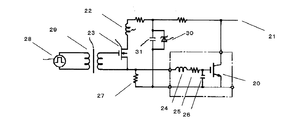
また、図12は特許文献2に記載された従来の半導体スイッチ駆動回路電源を高圧電源系から、降圧回路を介して所定の駆動電源を構成したものである。同図に示すように、半導体スイッチ20と、電源21と、電源21を半導体スイッチ20のゲート駆動電圧まで降圧する降圧回路を構成するインダクタンス22とトランジスタ23と、半導体スイッチ20におけるゲート発振防止回路を構成するインダクタンス24、抵抗25、コンデンサ26、抵抗27と、トランジスタ23を駆動する外部信号源28と、信号電圧用絶縁トランス29と、過電圧保護手段としてツナーダイオード30と、コンデンサ31から構成されるものである。
FIG. 12 shows a conventional semiconductor switch drive circuit power supply described in
この構成によれば、半導体スイッチ20駆動用の特別な電源を用いることなく、駆動電源21からインダクタンス22およびトランジスタスイッチ23を介して、半導体スイッチ20のゲート端子に所定の電源を供給することができる。しかしながら、半導体スイッチ20の駆動信号28は、降圧に設定された一定のデューティパルス状もしくは高周波信号と半導体スイッチ20の駆動信号とを重畳させたもので、トランス29を介して、トランジスタスイッチ23を駆動し、駆動電源21を降圧すると同時に所定の電圧を半導体スイッチ20のゲートに印加していた。
しかしながら、図10に示す従来の構成では、電源系統が少なくとも2系統必要となり、電源回路の構成部品点数増およびコストUPといった課題を有していた。
また、半導体スイッチ1におけるゲート駆動においては、オン時の速度は抵抗2とトランジスタ3の駆動能力で決定され、オフ時の速度は抵抗2’とトランジスタ3’の駆動能力で決定され、ハード的に決定されるので変更することができない。この種のスイッチング回路を設計時において、スイッチング速度を速めるには、抵抗2、2’の抵抗値を小さくすることが一般的ではあるが、しかしながら、この手法ではゲート電流のピーク電流が大きくなるとともに、半導体スイッチ1の負荷電流にも電流ひげが立ち、ノイズ発生、スイッチングロスの増加の原因となるといった課題を有していた。
However, the conventional configuration shown in FIG. 10 requires at least two power supply systems, and has problems such as an increase in the number of components of the power supply circuit and an increase in cost.
In the gate drive in the semiconductor switch 1, the on-speed is determined by the driving capability of the
また、一般的に、この種の半導体スイッチ特性として、駆動電流値および接合部温度により、スイッチング速度(オン、オフ時間)が変化するが、ゲート駆動波形が一定であるために、これら外的要因に対応することができない。この結果、課題として、想定される実使用範囲での最悪条件での設計となり、必要以上のデッドタイム設定が必要となり、スイッチング損失の増加、発生ノイズの増加など種々の課題を有していた。 In general, as a semiconductor switch characteristic of this type, the switching speed (on / off time) varies depending on the drive current value and the junction temperature. However, since the gate drive waveform is constant, these external factors Can not cope with. As a result, the design was made under the worst condition within the assumed actual usage range, and the dead time was set more than necessary, and there were various problems such as an increase in switching loss and an increase in generated noise.
また、図12に示す従来構成では、駆動信号28の発生時において、高周波成分を重畳させることが必要であるといった制約とともに、回路動作の時定数により追従性が悪くなるといった課題を有していた。
In addition, the conventional configuration shown in FIG. 12 has a problem that it is necessary to superimpose a high-frequency component when the
また、ゲート電圧を高電圧の駆動電源21から降圧しているために回り込みなどにより、ゲート耐圧破壊に至るといった信頼性に課題を有している。
Further, since the gate voltage is stepped down from the high-voltage
本発明は、前記従来の課題を解決するもので、半導体スイッチ用の駆動電源を不要とし、信頼性が高く、応答速度が速く、スイッチング特性にあわせた適切な駆動制御が可能といった半導体スイッチ回路半導体スイッチ回路およびその応用商品を提供することを目的とする。 The present invention solves the above-described conventional problems, and eliminates the need for a driving power source for a semiconductor switch, provides a high reliability, has a high response speed, and enables appropriate driving control in accordance with switching characteristics. An object is to provide a switch circuit and its application products.
前記従来の課題を解決するために、本発明の半導体スイッチ回路は、半導体スイッチと、電源供給手段と、電圧昇圧手段とを備え、前記電源供給手段の出力電圧は、前記半導体スイッチの動作電圧以下であることを特徴とするもので、電源供給手段における2次側回路が簡素化され部品点数が削減できる。また、常に半導体スイッチにおける最適なスイッチング速度を具現化するゲート駆動を電圧昇圧手段における昇圧動作で実現できる。さらに、ゲート電圧の充放電曲線を選択できるのでON時における突入電流やひげ電流がなくなり、ノイズ低減を実現する。また、半導体デバイスの温度・電流に応じ、駆動時間を制御できるのでスイッチング損失を低減できるようになる。とくに、降圧のための重畳信号発生が不要となり、信頼性面も不安がないといった特徴を有するものである。 In order to solve the conventional problem, a semiconductor switch circuit of the present invention includes a semiconductor switch, a power supply means, and a voltage boosting means, and an output voltage of the power supply means is equal to or lower than an operating voltage of the semiconductor switch. The secondary circuit in the power supply means is simplified and the number of parts can be reduced. In addition, the gate drive that always realizes the optimum switching speed in the semiconductor switch can be realized by the boosting operation in the voltage boosting means. Furthermore, since the charge / discharge curve of the gate voltage can be selected, inrush current and whisker current at the time of ON are eliminated and noise reduction is realized. Further, since the driving time can be controlled according to the temperature and current of the semiconductor device, the switching loss can be reduced. In particular, there is no need to generate a superimposed signal for stepping down, and there is a feature that there is no concern about reliability.
本発明によれば、半導体スイッチ用の駆動電源を不要とし、信頼性が高く、応答速度が速く、スイッチング特性にあわせた適切な駆動制御が可能といった半導体スイッチ回路半導体スイッチ回路およびその応用商品を提供できる。 According to the present invention, there is provided a semiconductor switch circuit, a semiconductor switch circuit, and an application product thereof that eliminates the need for a driving power source for a semiconductor switch, has high reliability, has a high response speed, and can perform appropriate drive control in accordance with switching characteristics. it can.
第1の発明は、半導体スイッチと、電源供給手段と、電圧昇圧手段とを備え、前記電源供給手段の出力電圧は、前記半導体スイッチの動作電圧以下であることを特徴とするもので、半導体スイッチ駆動手段用の電源供給手段を具備する必要がなくなり、半導体スイッチ回路の小型化・少部品化することができる。 A first invention includes a semiconductor switch, a power supply means, and a voltage boosting means, and an output voltage of the power supply means is lower than an operating voltage of the semiconductor switch. There is no need to provide power supply means for driving means, and the semiconductor switch circuit can be reduced in size and parts.
第2の発明は、半導体スイッチはMOSゲート型駆動素子であり、ゲート動作閾電圧は電源供給手段の出力電圧より大きい値であることを特徴とするもので、入力インピーダンスが高いことにより、駆動時に電荷の漏洩がすくないために、効率よく入力ゲート動作閾電圧Vth以上に電圧増幅が可能となり、半導体スイッチ回路の小型化・少部品化が可能である。 The second invention is characterized in that the semiconductor switch is a MOS gate type driving element, and the gate operation threshold voltage is larger than the output voltage of the power supply means. Since the leakage of electric charge is not high, the voltage can be efficiently amplified to the input gate operation threshold voltage Vth or higher, and the semiconductor switch circuit can be downsized and the number of parts can be reduced.
第3の発明は、電圧昇圧手段は、過電圧制限手段を有するもので、半導体スイッチのゲート端子の過電圧保護手段となり、半導体スイッチ回路の信頼性向上を図ることができる。 In the third invention, the voltage boosting means has an overvoltage limiting means, and serves as an overvoltage protection means for the gate terminal of the semiconductor switch, thereby improving the reliability of the semiconductor switch circuit.
第4の発明は、半導体スイッチ回路は、駆動電荷保持手段を有するもので、より効率よくオン駆動することが可能となり、効率よい駆動を実現することができる。 In the fourth aspect of the invention, the semiconductor switch circuit has the drive charge holding means, and can be turned on more efficiently, thereby realizing efficient drive.
第5の発明は、駆動電荷保持手段は、ダイオードおよび半導体スイッチ駆動端子入力容量に基づいて形成されるもので、電荷保持手段を構成する容量手段として半導体スイッチ駆動端子入力容量を用いて、ダイオードにより放電経路のインピーダンスを高くすることにより、放電時定数を構成することが可能となり、半導体スイッチ回路の駆動回路の小型化・少部品化を実現可能にすることができる。 According to a fifth aspect of the present invention, the drive charge holding means is formed based on a diode and a semiconductor switch drive terminal input capacitance, and a semiconductor switch drive terminal input capacitance is used as a capacitor means constituting the charge hold means. By increasing the impedance of the discharge path, it is possible to configure a discharge time constant, and it is possible to reduce the size and the number of parts of the drive circuit of the semiconductor switch circuit.
第6の発明は、電圧昇圧手段は、インダクタンスとON/OFFを繰り返す昇圧スイッチとから構成されることを特徴とするもので、電圧昇圧手段を、インダクタンスとON/OFFを繰り返す昇圧スイッチとから構成することにより、インダクタンスに蓄えられたエネルギーをもとに昇電圧(昇圧)することが可能となり、効率よく入力ゲート動作閾電圧Vth以上することができる
第7の発明は、昇圧スイッチにおけるスイッチ周波数もしくは昇圧スイッチにおけるON/OFFのデューティを変更することにより、電圧昇圧手段における出力電圧を変更することを特徴とするもので、昇圧スイッチにおけるON/OFF動作において、スイッチ周波数、もしくは昇圧スイッチのデューティ比率を可変することにより、半導体スイッチのゲート端子に印加される電圧値を可変したり、充電時間を変更することが可能となり、半導体スイッチの適切な駆動を実現することができる。
According to a sixth aspect of the present invention, the voltage boosting means is composed of an inductance and a boosting switch that repeats ON / OFF. The voltage boosting means is composed of a boosting switch that repeats the inductance and ON / OFF. By doing so, it becomes possible to increase the voltage (boost) based on the energy stored in the inductance, and to efficiently increase the input gate operation threshold voltage Vth or higher. The output voltage in the voltage boosting means is changed by changing the ON / OFF duty in the booster switch. In the ON / OFF operation in the booster switch, the switch frequency or the duty ratio of the booster switch is changed. By changing the semiconductor switch The voltage value applied to the gate terminal can be varied and the charging time can be changed, so that proper driving of the semiconductor switch can be realized.
第8の発明は、電圧昇圧手段における出力電圧を、半導体スイッチにおける接合部の温度に基づいて変更することを特徴とするもので、電圧昇圧手段における出力電圧を前記半導体スイッチにおける接合部温度により変更することにより、半導体デバイスのスイッチング速度特性の温度依存性をゲート駆動回路の電圧印加波形により補償することが可能となり、常に低損失のスイッチングおよび低ノイズ化を実現することができる。 The eighth invention is characterized in that the output voltage in the voltage boosting means is changed based on the temperature of the junction in the semiconductor switch, and the output voltage in the voltage boosting means is changed by the junction temperature in the semiconductor switch. As a result, the temperature dependence of the switching speed characteristics of the semiconductor device can be compensated by the voltage application waveform of the gate drive circuit, and low-loss switching and low noise can always be realized.
第9の発明は、電圧昇圧手段における出力電圧を、半導体スイッチに流れる電流値に基
づいて変更することを特徴とするもので、電圧昇圧手段における出力電圧を前記半導体スイッチにおける(負荷)電流値により変更することにより、半導体デバイスのスイッチング速度特性の電流依存性をゲート駆動回路の電圧印加波形により補償することが可能となり、常に低損失のスイッチングおよび低ノイズ化を実現することができる。
The ninth invention is characterized in that the output voltage in the voltage boosting means is changed based on the value of the current flowing in the semiconductor switch, and the output voltage in the voltage boosting means is changed by the (load) current value in the semiconductor switch. By changing, it becomes possible to compensate the current dependency of the switching speed characteristics of the semiconductor device by the voltage application waveform of the gate drive circuit, and it is possible to always realize low loss switching and low noise.
第10の発明は、半導体スイッチにおける接合部の温度を、前記半導体スイッチに設けたケルビン端子により検出することを特徴とするもので、接合温度検出を半導体スイッチに設けたケルビン端子により検出することにより、半導体デバイスのスイッチング速度特性の温度依存性をゲート駆動回路の電圧印加波形により補償することが可能となり、精度の高い温度検出を温度センサを設けることなく実現することができる。 The tenth invention is characterized in that the temperature of the junction in the semiconductor switch is detected by a Kelvin terminal provided in the semiconductor switch, and the junction temperature detection is detected by a Kelvin terminal provided in the semiconductor switch. The temperature dependence of the switching speed characteristics of the semiconductor device can be compensated by the voltage application waveform of the gate drive circuit, and highly accurate temperature detection can be realized without providing a temperature sensor.
第11の発明は、半導体スイッチと、半導体スイッチ駆動手段と、電圧昇圧手段とをモノリシックIC化したことを特徴とするもので、半導体スイッチ回路における駆動端子に電荷引抜き手段を具備することにより、半導体スイッチにおけるOFF時における動作が安定化および高速化が可能となり、スイッチングの安定化や損失低減を実現することができる。 The eleventh invention is characterized in that the semiconductor switch, the semiconductor switch driving means, and the voltage boosting means are made into a monolithic IC, and the semiconductor switching circuit is provided with charge extracting means at the driving terminal. The operation when the switch is OFF can be stabilized and speeded up, and switching can be stabilized and loss can be reduced.
第12の発明は、半導体スイッチと、半導体スイッチ駆動手段と、電圧昇圧手段とをモノリシックIC化したことを特徴とするもので、よりいっそう小型化が可能となり、しいては半導体スイッチング回路の小型化・軽量化を実現することができる。 The twelfth invention is characterized in that the semiconductor switch, the semiconductor switch driving means, and the voltage boosting means are made into a monolithic IC, which enables further miniaturization, and further miniaturization of the semiconductor switching circuit.・ Weight reduction can be realized.
第13の発明は、電源供給手段は、少なくとも半導体スイッチ手段と半導体スイッチ駆動手段へ伝達される元信号発生を行う制御手段との両手段へ、電力を供給することを特徴とするもので、少なくとも半導体スイッチ手段と半導体スイッチ手段を駆動する元信号の発生・制御手段との両手段に供給でき、電源構成が簡略化され、小型・少部品化とともに低ノイズ・高効率化を実現することができる。 In a thirteenth aspect of the present invention, the power supply means supplies power to at least both the semiconductor switch means and the control means for generating the original signal transmitted to the semiconductor switch drive means. It can be supplied to both the semiconductor switch means and the original signal generation / control means for driving the semiconductor switch means, the power supply configuration is simplified, and it is possible to realize low noise and high efficiency as well as downsizing and small parts. .
第14の発明は、上記請求項1〜13のいずれか1項に記載の半導体スイッチ回路を搭載したことを特徴とする電力変換装置で、省スペースとなり、小型の電力変換装置を実現することができる。 A fourteenth aspect of the present invention is a power conversion device including the semiconductor switch circuit according to any one of the first to thirteenth aspects, and can save space and realize a small-sized power conversion device. it can.
第15の発明は、上記請求項1〜13のいずれか1項に記載の半導体スイッチ回路を搭載したことを特徴とするインバータ装置で、省スペース、低ノイズ、低損失であるインバータ装置の実現が可能である。 A fifteenth aspect of the present invention is an inverter device comprising the semiconductor switch circuit according to any one of the first to thirteenth aspects, and can realize a space-saving, low noise, low loss inverter device. Is possible.
第16の発明は、上記請求項15記載のインバータ装置を搭載したことを特徴とする空気調和機で、室内外機における電装品のスペースが小型化ができ、発生ノイズ対策部品削減ができ、温度・電流によるスイッチング特性変動の補償が可能となり、低損失な空気調和機を実現することができる。 A sixteenth aspect of the present invention is an air conditioner equipped with the inverter device according to the fifteenth aspect described above, wherein the space for electrical components in the indoor / outdoor units can be reduced, noise generation countermeasure parts can be reduced, and the temperature can be reduced.・ Compensation for switching characteristics fluctuation due to current is possible, and a low-loss air conditioner can be realized.
以下、本発明の実施の形態について、図面を参照しながら説明する。なお、この実施の形態によって本発明が限定されるものではない。 Hereinafter, embodiments of the present invention will be described with reference to the drawings. Note that the present invention is not limited to the embodiments.
(実施の形態1)
図1は、本発明の第1の実施の形態におけるの構成図を示すものである。
(Embodiment 1)
FIG. 1 shows a configuration diagram in the first embodiment of the present invention.
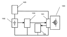
図1において、100は中耐圧の中型電流用FETなどのであり、101は半導体スイッチ駆動端子(ゲート端子)であり、102は電源供給手段DC電源(+5Vの出力電圧)であり、103は前記電源供給手段102からの電源電圧を(+15Vまでに)昇圧動作する電圧昇圧手段であり、104は半導体スイッチ駆動端子(ゲート端子)の電荷引き抜
き手段(小信号トランジスタ)であり、105は半導体スイッチ駆動手段101に対する過電圧制限手段(ツエナーダイオードなど)であり、それぞれが同図ように構成接続されたものである。
In FIG. 1,
以上のように構成された半導体スイッチ回路について、以下その動作、作用を説明する。 The operation and action of the semiconductor switch circuit configured as described above will be described below.
まず、図1を用いて動作の概要を説明し、以下、図2の回路図をもちいて回路動作を説明し、同じく図3を用いて本発明の他の実施の形態について説明をおこなう。以後、図4から図6を用いて、本発明の一実施の形態における回路定数を用いておこなったシュミレーション結果を引用し、回路動作の説明をおこなう。なお、図7〜図9は半導体スイッチの代表的な特性図であり、随時必要に応じて引用する。 First, the outline of the operation will be described with reference to FIG. 1, the circuit operation will be described with reference to the circuit diagram of FIG. 2, and another embodiment of the present invention will be described with reference to FIG. Hereinafter, the circuit operation will be described with reference to the simulation results performed using the circuit constants according to the embodiment of the present invention with reference to FIGS. 7 to 9 are typical characteristic diagrams of the semiconductor switch, and are quoted as needed.
まず、図1において、FETである半導体スイッチ手段100は、ゲート端子である半導体スイッチ駆動端子101をもっており、ゲートの閾値電圧(Vth)は、5〜8V程度であり、実際にオン動作時には+15Vを印加するのが一般的である。いっぽう、この半導体スイッチを駆動する信号源などを発生するマイコン、DSP、制御回路などは、通常5V程度の電源電圧で駆動されており、電源供給手段102から電源供給されている。半導体スイッチ100をオン動作するには、電源供給手段102からの+5Vの電源電圧を電圧昇圧手段103により、+15Vまで昇圧動作するとともに、半導体スイッチ駆動端子(ゲート端子)101へ駆動信号として供給することにより、オン動作をおこなうものである。
First, in FIG. 1, a semiconductor switch means 100, which is an FET, has a semiconductor
また、オフ時には、小信号トランジスタから構成される電荷引き抜き手段104により、半導体スイッチ駆動端子(ゲート端子)101の電荷(ゲート電圧)を引き抜くことにより、半導体スイッチ100をオフさせる。また、なんらかの異常で電圧昇圧手段103が異常となり、半導体スイッチ駆動端子101に過電圧が発生した場合には、ツエナーダイオードなどで構成される過電圧制限手段105が動作して、異常電圧を吸収し、半導体スイッチ駆動端子101を過電圧から保護するものである。また、半導体スイッチ100におけるオン/オフのスイッチング速度は、電圧昇圧手段103を単なるオン動作させるのではなく、半導体スイッチ100の動作周波数よりも充分高い周波数で駆動することにより、たとえばその周波数を変更したり、昇圧比を変更することにより実現できる。
When the switch is off, the
図2をもちいて、本発明の実施の形態について具体的な回路構成を持ちて説明をおこなう。 The embodiment of the present invention will be described with a specific circuit configuration with reference to FIG.
同図において、半導体スイッチ手段として用いたのは、N−chFET110であり、Vce450V、ドレイン電流20A、ゲート入力容量(同図において111で示す)が3000PF程度のものである。このFET110のゲートにはさらに、電荷引き抜き手段として小信号FET112および電荷保持手段としての小信号ダイオード113が接続されている。小信号FET112は、ドレイン電流1A程度のデバイスである。
In the figure, the N-
一方、小信号ダイオード113は、耐圧50V、順電流1A程度のIrrの少ない、高速スイッチダイオードである。また、小信号ダイオード113は、電圧昇圧手段を構成するインダクタンス116および昇圧スイッチの機能を果たすFET114に接続されている。このインダクタンス116は、インダクタンス67.5μF程度のものである。このFET114も、耐圧50V、ドレイン電流1A程度のデバイスである。この昇圧回路の整流および逆流防止機能としても、前記小信号ダイオード113は機能する。
On the other hand, the
なお、このスイッチ回路の電源としては、+5Vの出力をもつ直流電源115から構成
される。なお、この直流電源115は、本半導体スイッチ回路へ電源を供給するとともに、前記FET112およびFET114を駆動するスイッチング信号を発生するマイコンから構成される制御部(図示せず)へも電源供給している。すなわち、本発明の半導体スイッチ回路においては、従来、FET110を駆動するために必要なゲート電圧として+15V電源およびマイコンへの電源+5Vの両者が必要であったが、本実施の形態では電源115のみで同様の効果を実現することができている。
The power supply for this switch circuit is composed of a
また、図3は図2における一実施の形態における半導体スイッチ回路に、ダイオード119およびツエナーダイオード120から構成される、過電圧制限手段を具備したものである。ダイオード119は、耐圧50Vで順方向電圧の低いダイオード(たとえば、ショットキーダイオード)を用いている。また、ツエナーダイオード120は、クランプ電圧が5V程度のものであればよい。また、同図において抵抗器117は、通常ゲートとエミッタ間に入れられ、ゲート発振を防止し、スイッチング動作の安定を保証するものである。通常、1〜30KΩが使用される。また、抵抗器118は、FET112のオン時において、過電流を防止しかつFET110のオフ速度を決める抵抗器である。抵抗器117および抵抗器118は、本実施の形態においては、重要な意味をもつものではないが、回路動作上付加されるべきである。
FIG. 3 shows the semiconductor switch circuit according to the embodiment shown in FIG. 2 provided with overvoltage limiting means including a
このような構成での実施の形態において、回路動作を中心に説明する。 In the embodiment having such a configuration, the circuit operation will be mainly described.
図2において、電源115は+5Vであり、それよりもVthの高いFET110のゲートに印加しても、十分なオン状態を実現することはできない。しかしながら、電圧昇圧手段におけるFET114がオン時は、電源115とインダクタンス116をショート状態にでき、インダクタンスには、回路抵抗値などでのみ制限されるまでの電流を流すことができる。また、FET114のオン時間を変更することにより、インダクタンス116に流れる電流を制御することができる。すなわち、その際の電流値に応じて、Li2(J)の関係で決まる任意のエネルギーを蓄えることができる。
In FIG. 2, the
次に、このFET114がオフ動作となると、この蓄えられたエネルギーおよび電流は、回路が閉塞となるために、行き場所を失い、ダイオード113を介して、ゲート容量111へ流れ込む。このFET114のオン・オフを一定の周期で繰り返すことにより、ゲート容量111の両端電圧、すなわちゲート電圧となる。このゲート容量111に溜まった電荷は、ダイオード113に阻止されているために、リークする以外には消滅することはない。FET110をオンさせるだけであれば、以上説明したように、FET114を所定のオンオフデューティで駆動し、ゲート電圧が+15Vになり、FET110がオン状態になったところで、FET114のスイッチングを停止すれば、オン状態を維持することが可能である。しかしながら、FET110を任意のタイミングでオフされるには、ゲート容量111の電荷を引き抜き、ゲート電圧をVth以下に下げる必要がある。そのために、FET112をFET110のゲートとエミッタ間に接続し、FET112をON動作させることにより、ゲート容量を放電する。
Next, when the
また、何らかの要因により、昇圧手段の異常により、ゲート電圧がFET110のゲート保障電圧(通常はゲート酸化膜の耐圧に依存し、30V程度である)をこえると、破壊にいたるので、図3にしめす過電圧制限手段を用いる。この回路動作は、ゲート電圧が異常に上昇し、電源115(+5V)+ツエナー電圧(+5V)+ダイオード119のVf(0.7V)をこえた場合には、ツエナー電流がダイオード119およびツエナー120を介して、電源115へ流れ込むことにより、所定の電圧値以上にゲート電圧が上昇しないように機能する。これにより、FET110のゲート過電圧破壊を防止できるものである。
Also, for some reason, if the gate voltage exceeds the gate-guaranteed voltage of FET 110 (usually depends on the breakdown voltage of the gate oxide film and is about 30 V) due to an abnormality in the boosting means, it will be destroyed, so FIG. Use overvoltage limiting means. In this circuit operation, when the gate voltage rises abnormally and exceeds the power supply 115 (+5 V) + Zener voltage (+5 V) + Vf (0.7 V) of the
次に、図4〜図6をもちいて、電圧昇圧手段(回路)の動作をシュミレーション結果も用いて説明をおこなう。図4が、本実施の形態の図3における回路のうち、昇圧手段回路、すなわち直流電源115、インダクタンス116、小信号ダイオード113、FET114、FET110のゲート容量111の回路をシュミレーションモデル化したものであり、各構成部品の定数は同図に示すとおりである。本図において、P1はスイッチング周波数およびデューティ比を設定する発信回路である。この発振回路における周波数およびデューティ比により、スイッチSW1(FET114に相当)が動作する。
Next, the operation of the voltage boosting means (circuit) will be described using the simulation results with reference to FIGS. FIG. 4 shows a simulation model of the step-up circuit, that is, the circuit of the
図5は、SW1のオン/オフの一周期の動作を拡大したものである。SW1がオンすると、L1が電源Vdc1に短絡状態で接続されるために、インダクタンスL1および抵抗R1で制限される電流が流れる。この電流は、およそ一定の漸増特性を示しながら電流が増えていく。次にSW1がオフすると、L1に流れる電流は、また一定の漸減特性を示しながら現象する。 FIG. 5 is an enlarged view of the operation of one cycle of SW1 on / off. When SW1 is turned on, L1 is connected to the power supply Vdc1 in a short-circuited state, so that a current limited by the inductance L1 and the resistor R1 flows. This current increases while showing a substantially constant gradual increase characteristic. Next, when SW1 is turned off, the current flowing through L1 again exhibits a constant gradual decrease characteristic.
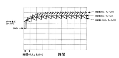
この電流は、流れる経路が遮断されているために、ダイオードD1を介して、コンデンサC1(ゲート容量)へ流れ込み、ゲート電圧を上昇させる。Vg=Q*C=I*dT*Cで示される電圧まで上昇する。図6に示すように、このSW1のオンオフを繰り返すことにより、ゲート電圧を昇圧制御することが可能となる。同図においては、SW1のスイッチ動作、L1の電流およびゲート電圧の時間的な変化を表記している。同図は、図4の回路において、5KHzのスイッチング周波数で50%デューティにてスイッチングを繰り返した場合の波形であり、役1.6μSでゲート電圧が+15Vまで昇圧されていることがわかる。 Since the flow path is cut off, this current flows into the capacitor C1 (gate capacitance) via the diode D1 and raises the gate voltage. The voltage rises to the voltage indicated by Vg = Q * C = I * dT * C. As shown in FIG. 6, the gate voltage can be boosted by repeatedly turning on and off SW1. In the figure, the switch operation of SW1, the current of L1, and the temporal change of the gate voltage are shown. This figure shows the waveform when switching is repeated at 50% duty with a switching frequency of 5 KHz in the circuit of FIG. 4, and it can be seen that the gate voltage is boosted to +15 V at 1.6 μS.
また、このSW1のスイッチング周期(周波数)およびデューティを変更することにより、いわゆる昇圧比を変えることが可能となり、ゲート電圧を変更したり、またゲート電圧を駆動時の立ち上がり時の立ち上がり時定数を変更制御することが可能である。図7において、同じ図3における回路で、デューティ比が同じ50%でスイッチング周波数を2.5KHz、5KHzの場合、また同じスイッチング周波数が5KHzの場合にデューティ比を1%、50%に変更した場合のゲート電圧の立ち上がり状態を示す。同図から明らかに、本実施の形態における電圧昇圧手段におけるスイッチング状態を変更すると、FETの駆動速度を制御することが可能であることがわかる。 Also, by changing the SW1 switching cycle (frequency) and duty, it is possible to change the so-called step-up ratio, change the gate voltage, or change the rise time constant when the gate voltage is driven. It is possible to control. 7, in the same circuit in FIG. 3, when the duty ratio is 50% and the switching frequency is 2.5 KHz and 5 KHz, and when the same switching frequency is 5 KHz, the duty ratio is changed to 1% and 50%. The rising state of the gate voltage is shown. From the figure, it is apparent that the driving speed of the FET can be controlled by changing the switching state of the voltage boosting means in the present embodiment.
以上、図4におけるシュミレーションモデルを用いて説明をおこなったが、本実施の形態の図3においても、同様の結果が得られる。 Although the description has been given above using the simulation model in FIG. 4, similar results are obtained also in FIG. 3 of the present embodiment.
また、この種の用途で一般的な半導体スイッチとしてIGBTがある。このIGBTの代表的な特性として、図7に示すようなオン・オフのスイッチング時間の温度依存性と電流依存性がある。同図において、横軸はIGBTがドライブするコレクタ電流値であり、縦軸はオン時間およびオフ時間を示すスイッチ時間である。ここでプロットされているのは、同じゲート抵抗とゲート駆動電圧を印加した常態での、あるIGBT接合部温度(ジャンクション温度)が25℃と125℃時のオン速度、オフ速度を示している。 In addition, there is an IGBT as a general semiconductor switch for this type of application. Typical characteristics of the IGBT include temperature dependency and current dependency of on / off switching time as shown in FIG. In the figure, the horizontal axis represents the collector current value driven by the IGBT, and the vertical axis represents the switch time indicating the on time and the off time. Plotted here are the on-speed and off-speed when the IGBT junction temperature (junction temperature) is 25 ° C. and 125 ° C. in a normal state where the same gate resistance and gate drive voltage are applied.
TON、TOFFはそれぞれ、オン・オフ時のスイッチング時間を示し、Tr、Tfはそれぞれオン・オフ時における電流の立ち上がり、立下り時間を示している。すべて、高速であるほうがIGBTデバイスとして、高速スイッチングを実現しているといえる。ここでの課題としては、同図から明らかなように、温度・電流値でIGBTのスイッチング速度が変化することである。この変化は、実回路アプリケーションにおいては、たとえばインバータ制御においては、上下アーム短絡防止のデッドタイム設定に影響において、もっとも時間的な遅れが発生する状態でも、アーム短絡しないような十分マージンを持ったデッドタイムを設定する必要があり、通常時においてはインバータ出力効率の低下やロス
を増加させることになる。
TON and TOFF indicate the switching time during on / off, respectively, and Tr and Tf indicate the rise and fall times of the current during on / off, respectively. It can be said that high-speed switching is realized as an IGBT device at higher speeds. The problem here is that the switching speed of the IGBT changes depending on the temperature and current values, as is apparent from FIG. In actual circuit applications, for example, in inverter control, the dead time setting has a sufficient margin to prevent arm short-circuiting even in the most time-delayed state due to the influence of the dead time setting for preventing upper and lower arm short-circuiting It is necessary to set the time, and in a normal time, the inverter output efficiency is reduced and the loss is increased.
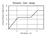
また、スイッチング電源のようなエミッタ設置での駆動においても、オンオフデューティの設定限界として、スイッチング遅れが関係するので、電源変換効率を低下させることになっていた。この課題に対して、本実施の形態では、すでに述べたように図7に示すように、電圧昇圧手段におけるFET14における周波数を変更やオンオフデューティ比を変更することにより、ゲート電圧の立ち上がり速度を変更することができ、スイッチング速度変更することが可能となっている。一般的に、ゲートにおけるチャージ電荷量とゲート電圧との関係をしましたものが図9である。同図において、ゲートチャージ量とともに、ゲート電圧が上昇し、閾値電圧(同図において水平な部分)の動作領域を経て、オンすることがわかる。この図からわかるように、すばやくゲートに電荷を充電することが高速にオンさせることであり、このチャージ充放電時間でスイッチング速度を制御できる。本実施れいにおいては、電圧昇圧回路における動作を制御することにより、変更することが可能である。 Further, even in the case of driving with an emitter such as a switching power supply, since the switching delay is related as the setting limit of the on / off duty, the power conversion efficiency is reduced. In response to this problem, in the present embodiment, as described above, the rising speed of the gate voltage is changed by changing the frequency of the FET 14 in the voltage boosting means or changing the on / off duty ratio as shown in FIG. It is possible to change the switching speed. In general, FIG. 9 shows the relationship between the charge amount at the gate and the gate voltage. In the figure, it can be seen that the gate voltage increases with the amount of gate charge, and is turned on via the operating region of the threshold voltage (horizontal portion in the figure). As can be seen from this figure, quickly charging the gate with charge is turning on at high speed, and the switching speed can be controlled by this charge / discharge time. This embodiment can be changed by controlling the operation of the voltage booster circuit.
すなわち、FET110における接合部の温度、および駆動電流を検出して、所定のスイッチング速度を実現するゲート駆動制御を前記FET114の制御をおこなうことにより、実現している。また、温度検出手段として、FET110にケルビン端子(温度依存性のあるPN接合端子)を用いることにより、より精度がたかくレスポンスの早いスイッチング制御を行うことができる。
That is, the gate drive control for realizing a predetermined switching speed by detecting the temperature of the junction and the drive current in the
また、上記関連回路は、すべてモノリシックIC化が可能であり、IC化することにより、さらに半導体スイッチ回路全体の小型化を実現することが可能である。 The related circuits can all be monolithic ICs, and by making them ICs, it is possible to further reduce the size of the entire semiconductor switch circuit.
また、本発明の半導体スイッチ回路を搭載した電力変換装置においては、電源回路が小型化でき、ゲート充電電流の立ち上がりを制御できるので、ゲートオン時におけるサージ電流を防止でき、ノイズ低減を実現できるとともに、システム全体を小型化することが可能である。 Further, in the power conversion device equipped with the semiconductor switch circuit of the present invention, the power supply circuit can be miniaturized and the rise of the gate charging current can be controlled, so that the surge current at the time of turning on the gate can be prevented, and noise reduction can be realized. It is possible to reduce the size of the entire system.
また、本発明の半導体スイッチ回路を搭載したインバータ装置においては、半導体スイッチのスイッチング速度を温度、電流応じて制御することが容易であるので、インバータ装置のデッドタイムを最適な状態に保つことが可能であり、システム効率の向上を実現できる。 Further, in the inverter device equipped with the semiconductor switch circuit of the present invention, it is easy to control the switching speed of the semiconductor switch according to the temperature and current, so that the dead time of the inverter device can be kept in an optimum state. It is possible to improve the system efficiency.
また、本発明の半導体スイッチ回路を搭載した空気調和機においては、半導体スイッチのスイッチング速度を温度、電流応じて制御することが容易であるので、ノイズ低減を実現できるとともに、電装品ばかりではなくヒートシンクの形状を小型化できるので電装品を小型化することが可能となり、熱交換器や風回路を大きく効率よくすることが可能であるばかりでなく、インバータ装置のデッドタイムを最適な状態に保つことが可能であり、製品効率の向上を実現でき、省エネのインバータ空気調和機を実現できる。 Further, in the air conditioner equipped with the semiconductor switch circuit of the present invention, it is easy to control the switching speed of the semiconductor switch according to the temperature and current, so that noise can be reduced and not only the electrical components but also the heat sink can be realized. The size of the electrical equipment can be reduced, so it is possible to reduce the size of the electrical components, and not only can the heat exchanger and wind circuit be made large and efficient, but also the dead time of the inverter device can be maintained in an optimum state. Therefore, it is possible to improve product efficiency and realize an energy-saving inverter air conditioner.
以上のように、本実施の形態においては半導体スイッチ回路を電源供給手段と、出力電圧が前記半導体スイッチの動作電圧以下である電圧昇圧手段とを備えたものとすることにより、電源供給手段の電源をゲート電圧まで昇圧動作することにより、小型化・低ノイズ化・高効率化することができる。 As described above, in this embodiment, the semiconductor switch circuit includes the power supply means and the voltage boosting means whose output voltage is equal to or lower than the operating voltage of the semiconductor switch. Can be reduced in size, reduced in noise, and improved in efficiency.
また、上記実施の形態においては、半導体スイッチにおいて、おもにFETを用いて説明を行ったが、IGBTなどのゲート駆動型の半導体デバイスであれば同等の効果を得ることができる。 Further, in the above-described embodiment, the semiconductor switch has been described mainly using the FET. However, an equivalent effect can be obtained if it is a gate drive type semiconductor device such as an IGBT.
また、本発明の実施の形態においては、半導体デバイスの特性変動要因として、温度および電流値に関して説明を行ったが、当然スイッチング速度検出手段を設け、その検出値をもとに本実施の形態におけるようなスイッチング帰還制御を設ければ、個々の半導体デバイスにおけるいわゆる特性ばらつきを均一化することが可能である。 In the embodiment of the present invention, the temperature and the current value have been described as the characteristic variation factors of the semiconductor device. However, naturally, a switching speed detecting means is provided, and the present embodiment is based on the detected value. If such switching feedback control is provided, so-called characteristic variations in individual semiconductor devices can be made uniform.
また、本発明における実施の形態において説明した回路構成は、一実施の形態を示すものであり、同様の機能を実現する他の回路手段、制御手段を用いても同様の効果を得ることが可能である。 The circuit configuration described in the embodiment of the present invention shows an embodiment, and the same effect can be obtained even if other circuit means and control means that realize the same function are used. It is.
以上のように、本発明にかかる半導体スイッチ回路は、簡易な単一出力の電源構成で、半導体スイッチの駆動を諸条件に合わせて適切な駆動条件変更が可能となるので、スイッチング電源や電力変換コンバータやインバータ装置や車載における半導体スイッチ回路などの用途にも適用できる。 As described above, the semiconductor switch circuit according to the present invention has a simple single-output power supply configuration, and the driving condition of the semiconductor switch can be changed appropriately according to various conditions. It can also be applied to applications such as converters, inverter devices and in-vehicle semiconductor switch circuits.
100 半導体スイッチ手段
101 半導体スイッチ駆動端子(ゲート端子)
102 電源供給手段
103 電圧昇圧手段
104 電荷引き抜き手段(小信号トランジスタ)
105 過電圧制限手段(ツエナーダイオード)
100 Semiconductor switch means 101 Semiconductor switch drive terminal (gate terminal)
102 power supply means 103 voltage boosting means 104 charge extracting means (small signal transistor)
105 Overvoltage limiting means (Zener diode)
Claims (16)
Priority Applications (1)
| Application Number | Priority Date | Filing Date | Title |
|---|---|---|---|
| JP2004227938A JP2006050776A (en) | 2004-08-04 | 2004-08-04 | Semiconductor switch circuit, power conversion device, inverter device, and air-conditioner |
Applications Claiming Priority (1)
| Application Number | Priority Date | Filing Date | Title |
|---|---|---|---|
| JP2004227938A JP2006050776A (en) | 2004-08-04 | 2004-08-04 | Semiconductor switch circuit, power conversion device, inverter device, and air-conditioner |
Publications (1)
| Publication Number | Publication Date |
|---|---|
| JP2006050776A true JP2006050776A (en) | 2006-02-16 |
Family
ID=36028669
Family Applications (1)
| Application Number | Title | Priority Date | Filing Date |
|---|---|---|---|
| JP2004227938A Pending JP2006050776A (en) | 2004-08-04 | 2004-08-04 | Semiconductor switch circuit, power conversion device, inverter device, and air-conditioner |
Country Status (1)
| Country | Link |
|---|---|
| JP (1) | JP2006050776A (en) |
Cited By (6)
| Publication number | Priority date | Publication date | Assignee | Title |
|---|---|---|---|---|
| JP2008182835A (en) * | 2007-01-25 | 2008-08-07 | Mitsubishi Electric Corp | Semiconductor device |
| JP2009106072A (en) * | 2007-10-23 | 2009-05-14 | Rohm Co Ltd | Overvoltage protection circuit and electronic apparatus using the same |
| JP2010142037A (en) * | 2008-12-12 | 2010-06-24 | Denso Corp | Power conversion device |
| JP2012147646A (en) * | 2011-01-14 | 2012-08-02 | Panasonic Corp | Load control device |
| WO2017026367A1 (en) * | 2015-08-07 | 2017-02-16 | 三菱電機株式会社 | Power switching apparatus |
| WO2018198211A1 (en) * | 2017-04-25 | 2018-11-01 | 新電元工業株式会社 | Switching element control circuit and power module |
-
2004
- 2004-08-04 JP JP2004227938A patent/JP2006050776A/en active Pending
Cited By (13)
| Publication number | Priority date | Publication date | Assignee | Title |
|---|---|---|---|---|
| JP2008182835A (en) * | 2007-01-25 | 2008-08-07 | Mitsubishi Electric Corp | Semiconductor device |
| JP2009106072A (en) * | 2007-10-23 | 2009-05-14 | Rohm Co Ltd | Overvoltage protection circuit and electronic apparatus using the same |
| JP2010142037A (en) * | 2008-12-12 | 2010-06-24 | Denso Corp | Power conversion device |
| JP2012147646A (en) * | 2011-01-14 | 2012-08-02 | Panasonic Corp | Load control device |
| CN107980199A (en) * | 2015-08-07 | 2018-05-01 | 三菱电机株式会社 | Power switch device |
| KR20180023980A (en) * | 2015-08-07 | 2018-03-07 | 미쓰비시덴키 가부시키가이샤 | Power switching device |
| WO2017026367A1 (en) * | 2015-08-07 | 2017-02-16 | 三菱電機株式会社 | Power switching apparatus |
| JPWO2017026367A1 (en) * | 2015-08-07 | 2018-05-10 | 三菱電機株式会社 | Power switching device |
| KR101970112B1 (en) | 2015-08-07 | 2019-04-17 | 미쓰비시덴키 가부시키가이샤 | Power switching device |
| US10651839B2 (en) | 2015-08-07 | 2020-05-12 | Mitsubishi Electric Corporation | Power switching apparatus |
| WO2018198211A1 (en) * | 2017-04-25 | 2018-11-01 | 新電元工業株式会社 | Switching element control circuit and power module |
| GB2577182A (en) * | 2017-04-25 | 2020-03-18 | Shindengen Electric Mfg | Switching element control circuit and power module |
| GB2577182B (en) * | 2017-04-25 | 2022-02-02 | Shindengen Electric Mfg | Switching element control circuit and power module |
Similar Documents
| Publication | Publication Date | Title |
|---|---|---|
| CN101079576B (en) | System for providing switch of power adjuster | |
| US5610503A (en) | Low voltage DC-to-DC power converter integrated circuit and related methods | |
| US6885225B2 (en) | Drive circuit | |
| KR100760085B1 (en) | Switching Power Supply Device and Switching Method | |
| KR100731393B1 (en) | Switching regulator | |
| US20160315553A1 (en) | Rectifier, Alternator, and Power Converter | |
| US8294443B2 (en) | Overshoot/undershoot elimination for a PWM converter which requires voltage slewing | |
| JPWO2016002249A1 (en) | Switching circuit and power supply circuit having the same | |
| CN111771321B (en) | Semiconductor switch control circuit and switching power supply device | |
| JP2010200554A (en) | Dc-dc converter | |
| CN105186859B (en) | Switching converter and method for discharging output terminal thereof | |
| US10715027B2 (en) | Driver circuit | |
| KR101758808B1 (en) | Intelligent Power Module And Power Driving Module Thereof | |
| US7151328B2 (en) | Auxiliary power source and method for operating the auxiliary power source, as well as circuit arrangement for switching a load | |
| EP3832866B1 (en) | Overcurrent protection circuit and switching circuit | |
| US6781432B2 (en) | Control circuit of MOSFET for synchronous rectification | |
| JP5407618B2 (en) | Gate drive circuit and power conversion circuit | |
| US9484801B2 (en) | Start-up regulator for high-input-voltage power converters | |
| JPWO2007091374A1 (en) | Synchronous rectification forward converter | |
| JP2000134075A (en) | Switch device | |
| EP2391184A2 (en) | Led driver circuit | |
| JP2006050776A (en) | Semiconductor switch circuit, power conversion device, inverter device, and air-conditioner | |
| JP4013011B2 (en) | Switching power supply circuit | |
| JP6910115B2 (en) | Active snubber circuit | |
| US20220271670A1 (en) | Converter with hold-up circuit and inrush-control circuit |