JP2006013674A - Radio transmission circuit and transmitter-receiver employing the same - Google Patents
Radio transmission circuit and transmitter-receiver employing the same Download PDFInfo
- Publication number
- JP2006013674A JP2006013674A JP2004184779A JP2004184779A JP2006013674A JP 2006013674 A JP2006013674 A JP 2006013674A JP 2004184779 A JP2004184779 A JP 2004184779A JP 2004184779 A JP2004184779 A JP 2004184779A JP 2006013674 A JP2006013674 A JP 2006013674A
- Authority
- JP
- Japan
- Prior art keywords
- circuit
- frequency
- output
- delta modulator
- sigma delta
- Prior art date
- Legal status (The legal status is an assumption and is not a legal conclusion. Google has not performed a legal analysis and makes no representation as to the accuracy of the status listed.)
- Granted
Links
Images


Classifications
-
- H—ELECTRICITY
- H04—ELECTRIC COMMUNICATION TECHNIQUE
- H04B—TRANSMISSION
- H04B1/00—Details of transmission systems, not covered by a single one of groups H04B3/00 - H04B13/00; Details of transmission systems not characterised by the medium used for transmission
- H04B1/005—Details of transmission systems, not covered by a single one of groups H04B3/00 - H04B13/00; Details of transmission systems not characterised by the medium used for transmission adapting radio receivers, transmitters andtransceivers for operation on two or more bands, i.e. frequency ranges
- H04B1/0053—Details of transmission systems, not covered by a single one of groups H04B3/00 - H04B13/00; Details of transmission systems not characterised by the medium used for transmission adapting radio receivers, transmitters andtransceivers for operation on two or more bands, i.e. frequency ranges with common antenna for more than one band
- H04B1/006—Details of transmission systems, not covered by a single one of groups H04B3/00 - H04B13/00; Details of transmission systems not characterised by the medium used for transmission adapting radio receivers, transmitters andtransceivers for operation on two or more bands, i.e. frequency ranges with common antenna for more than one band using switches for selecting the desired band
Landscapes
- Engineering & Computer Science (AREA)
- Computer Networks & Wireless Communication (AREA)
- Signal Processing (AREA)
- Stabilization Of Oscillater, Synchronisation, Frequency Synthesizers (AREA)
- Transmitters (AREA)
Abstract
Description
本発明は移動体通信機用送信回路に係り、特に大規模集積化に適した無線送信回路及びそれを送信回路部に適用した送受信機に関する。 The present invention relates to a transmission circuit for a mobile communication device, and more particularly to a radio transmission circuit suitable for large-scale integration and a transmitter / receiver to which the transmission circuit unit is applied.
移動体通信機の爆発的な普及につれ、小型、低コスト化への要求が強まっている。そのため集積度を高めた送受信集積回路の適用が望まれている。集積度をあげた送受信機用集積回路の従来例の1つとしては日立製作所により2001年に発表されている(非特許文献1参照)。これはオフセットPLL送信回路を適用しており、送信機にはRF周波数帯位相同期ループ(PLL)、中間(IF)周波数帯PLLのほか送信発振器の計3つの発振回路およびそれを含むPLL回路が存在する。 With the explosive spread of mobile communication devices, there is an increasing demand for miniaturization and cost reduction. Therefore, application of a transmission / reception integrated circuit with an increased degree of integration is desired. One example of a conventional integrated circuit for a transmitter / receiver having an increased degree of integration was announced by Hitachi, Ltd. in 2001 (see Non-Patent Document 1). This uses an offset PLL transmission circuit, and the transmitter has a total of three oscillation circuits including an RF frequency band phase locked loop (PLL), an intermediate (IF) frequency band PLL, and a transmission oscillator, and a PLL circuit including the oscillation circuit. Exists.
また、デジタル入力とデルタ・シグマ(ΔΣ)変調器との間に、当該デジタル入力から離散的に変化しかつ時間平均が当該デジタル入力と一致するデジタル出力をΔΣ変調器へ供給するデジタルディザ回路が設けられた変調型分数分周PLL周波数シンセサイザを用いる携帯電話の構成が知られている(例えば、特許文献1参照)。なお、以下では「デルタ・シグマ変調器」は、一般的には「シグマデルタ(ΣΔ)変調器」と呼ばれているので、「シグマデルタ(ΣΔ)変調器」を用いることとする。 In addition, a digital dither circuit is provided between the digital input and the delta-sigma (ΔΣ) modulator, and supplies a digital output that changes discretely from the digital input and whose time average matches the digital input to the ΔΣ modulator. A configuration of a cellular phone using a provided modulation type frequency division PLL frequency synthesizer is known (see, for example, Patent Document 1). In the following description, the “delta sigma modulator” is generally referred to as a “sigma delta (ΣΔ) modulator”, and therefore the “sigma delta (ΣΔ) modulator” is used.
前者の従来例では、TX(送信周波数)用、RF(高周波数)用、IF周波数用の計3つの発振器を必要とする。これら発振器を集積しようとした場合は、いずれの発振器に対しても低雑音性が要求されるため集積回路上で面積を専有するサイズの大きなインダクタが必要となり、小型化が困難であった。 The former conventional example requires a total of three oscillators for TX (transmission frequency), RF (high frequency), and IF frequency. When these oscillators are to be integrated, a low-noise property is required for any of the oscillators, so a large-sized inductor that occupies a large area on the integrated circuit is required, and it is difficult to reduce the size.
後者の従来例では、例えば、1つのPLLを使ってIF,RF両方の局部発振信号を発生する回路構成が開示されているが、これらの周波数配置に対して発生するスプリアスに対する検討が成されていない。また、このような局部発振器に用いるシンセサイザに好適なΣΔシンセサイザに関しても言及し、ΣΔシンセサイザ特有のスプリアスの問題を解決する際に、ディザ回路の必要性は述べているが、スプリアスの問題を回避すると共に更に小型化を可能にする具体的な構成については述べられていない。 In the latter conventional example, for example, a circuit configuration that generates both IF and RF local oscillation signals using a single PLL is disclosed, but studies on spurious generated for these frequency arrangements have been made. Absent. It also refers to a ΣΔ synthesizer suitable for a synthesizer used for such a local oscillator, and avoids the spurious problem, although the necessity of a dither circuit is described in solving the spurious problem peculiar to the ΣΔ synthesizer. In addition, a specific configuration that enables further miniaturization is not described.
そこで、本発明の目的は、スプリアスの問題を回避すると共に小型化に適し、部品点数を低減でき、高集積可能な送信回路を提供することにある。 SUMMARY OF THE INVENTION An object of the present invention is to provide a transmission circuit that avoids the problem of spurious and is suitable for miniaturization, can reduce the number of components, and can be highly integrated.
また、上記送信回路を用いた送受信機を提供することも目的の一つである。 Another object is to provide a transceiver using the transmission circuit.
本発明の代表的手段の一例を示せば、次の通りである。すなわち、本発明に係る送信回路は、第1の周波数発生回路と、第1の周波数変換回路と、前記第1の周波数変換回路の出力が入力される第2の周波数変換回路と、第1の分周回路部とを具備し、前記第1の周波数発生回路の出力が、前記第1の分周回路部を介して前記第1の周波数変換回路の局部発振信号として供給され、前記第1の周波数発生回路の出力が、直接または第2の分周回路部を介して前記第2の周波数変換回路の局部発振信号として供給され、前記第1の分周回路部の分周数が可変に設定されて成ることを特徴とするものである。ここで上記各回路は、図1で言えば、第1の周波数発生回路はシンセサイザSS、第1の周波数変換回路は直交変調器8、第2の周波数変換回路はオフセットPLL、第1の分周回路部は分周器30,31、第2の分周回路部は27,29にそれぞれ対応する。
An example of typical means of the present invention is as follows. That is, a transmission circuit according to the present invention includes a first frequency generation circuit, a first frequency conversion circuit, a second frequency conversion circuit to which an output of the first frequency conversion circuit is input, And an output of the first frequency generation circuit is supplied as a local oscillation signal of the first frequency conversion circuit through the first frequency division circuit, The output of the frequency generation circuit is supplied as a local oscillation signal of the second frequency conversion circuit directly or via the second frequency division circuit unit, and the frequency division number of the first frequency division circuit unit is set to be variable It is characterized by being made. Here, each of the above circuits is the same as in FIG. 1. The first frequency generating circuit is the synthesizer SS, the first frequency converting circuit is the
本発明によれば、RF周波数帯PLLとIF周波数帯PLLとを1つのPLLシンセサイザで兼用するので、必要な発振器の個数を低減でき、無線送信回路が小型化する。 According to the present invention, since the RF frequency band PLL and the IF frequency band PLL are shared by one PLL synthesizer, the number of necessary oscillators can be reduced and the radio transmission circuit can be downsized.
以下、添付図面を参照しながら、本発明の実施例を詳細に説明する。 Hereinafter, embodiments of the present invention will be described in detail with reference to the accompanying drawings.
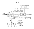
本発明の第1の実施例について、図1〜4を用いて説明する。図1は、本発明に係る無線送信回路を適用した送受信回路を集積化したRFICの構成を示す図である。本RFIC34は、GSM850,GSM900,DCS1800,PCS1900の4つの周波数帯に対応するものである。
A first embodiment of the present invention will be described with reference to FIGS. FIG. 1 is a diagram showing a configuration of an RFIC in which transmission / reception circuits to which a wireless transmission circuit according to the present invention is applied are integrated. This
GSM850は、送信帯域が824MHz〜849MHz、受信帯域が869MHz〜894MHzである。GSM900は、送信帯域が880MHz〜915MHz、受信帯域が925MHz〜960MHzである。DCS1800は、送信帯域が1710MHz〜1785MHz、受信帯域が1805MHz〜1880MHzである。PCS1900は、送信帯域が1850MHz〜1910MHz、受信帯域が1930MHz〜1990MHzである。 GSM850 has a transmission band of 824 MHz to 849 MHz and a reception band of 869 MHz to 894 MHz. GSM900 has a transmission band of 880 MHz to 915 MHz and a reception band of 925 MHz to 960 MHz. The DCS 1800 has a transmission band of 1710 MHz to 1785 MHz and a reception band of 1805 MHz to 1880 MHz. The PCS 1900 has a transmission band of 1850 MHz to 1910 MHz and a reception band of 1930 MHz to 1990 MHz.
受信信号は、アンテナANTから入る妨害波を除去するためのフィルタ回路であるバンドパスフィルタ(BPF)1を介して集積回路上の低雑音増幅器(LNA)2に入力される。低雑音増幅器によって増幅された信号は、ミキサ回路(MIX)3によって周波数変換されI,Q2つのベースバンド信号に変換される。ベースバンド信号は、利得可変増幅器(PGA)と周波数変換された妨害波を除去するためのフィルタ(LPF)とが合成されたPGA/LPF回路5をそれぞれ通り、出力I,Q信号としてRFIC34から出力される。
The received signal is input to a low noise amplifier (LNA) 2 on an integrated circuit via a band pass filter (BPF) 1 which is a filter circuit for removing an interference wave entering from the antenna ANT. The signal amplified by the low noise amplifier is frequency-converted by a mixer circuit (MIX) 3 and converted into two baseband signals I and Q. The baseband signal passes through the PGA /
ミキサ回路3に入力されるローカル信号は、電圧制御発振器(VCO)21の出力信号を分周することで生成される。GSM850、GSM900の場合は、2分周器32がスイッチ33により選択され、更に2分周器4にて合計4分周されてミキサ3を駆動する。DCS1800、PCS1900の場合は、スイッチ33にて2分周器32を非選択とし、計2分周した信号がミキサ3を駆動する。このように分周器を適用することで、正確に90度位相のずれたI,Q用の局部発振信号を生成出来る。VCO21は、可変分周器(DIV)22、位相比較器(PD)23、チャージポンプ回路(CP)24、ループフィルタ(LF)25と合わせて構成されるシンセサイザSSにより安定した周波数制御のもとで動作する。可変分周器22の分周数は制御回路(CONT)26によって設定され、所望の発振周波数に制御できる。
The local signal input to the
送信回路は、GMSK(Gaussian filtered Minimum Shift Keying)変調信号に対応するものであり、入力信号はI,Qの2系統である。入力信号は、信号レベルを後段の直交変調器8に合わせるためのアッテネータ回路6と、帯域外雑音を低減する低域通過フィルタ7を介して直交変調器8に印加される。直交変調器の出力であるIF信号は、リミッタ回路10を介して位相比較器11を駆動する。位相比較器の出力は、ループフィルタ12を介して送信用VCO13の制御電圧を制御する。VCO13の出力には、4分周器14と2分周器15が取りつけられている。
The transmission circuit corresponds to a GMSK (Gaussian filtered Minimum Shift Keying) modulated signal, and input signals are two systems of I and Q. The input signal is applied to the
GSM850,GSM900帯の送信信号は4分周器14より出力され、DCS1800,PCS1900帯の送信信号は、2分周器15より出力される。送信信号は、ミキサ16にてIF信号帯に周波数変換され、位相比較回路11にて入力IF信号との誤差が検出され、VCO13に帰還される。この結果、各分周器14,15の出力に所定の中心周波数をもつGMSK変調信号を発生させる事が出来る。分周器14の出力は電力増幅器17(GSM850,900用)にて増幅され、分周器15の出力は電力増幅器18(DCS1800、PCS1900用)にて増幅される。増幅された送信信号は、それぞれ低域通過フィルタ(LPF)19,20にて高調波が取り除かれ、スイッチS/W21を介してアンテナに放出される。
The GSM850 and GSM900 band transmission signals are output from the
このような送信回路はオフセットPLL回路(O−PLL)として知られているが、直交変調器を駆動するIF局部発振信号と、PLLの帰還ループ内のミキサ回路を駆動するRF局部発振信号が必要となる。先にも述べたように従来では2つの個別のシンセサイザにより、これらの信号を発生させていたが、本実施例では1つのシンセサイザにより発生させて小型化を図っている。 Such a transmission circuit is known as an offset PLL circuit (O-PLL), but requires an IF local oscillation signal that drives the quadrature modulator and an RF local oscillation signal that drives the mixer circuit in the feedback loop of the PLL. It becomes. As described above, conventionally, these signals are generated by two individual synthesizers. However, in this embodiment, the signals are generated by one synthesizer to reduce the size.
受信回路の局部発振信号生成用として用いてきたVCO21を送信用RF,IF信号生成用としても活用する。RF局部発振信号は、VCO21の出力を分周することにより発生させる。具体的には、GSM850,900用としては2つの2分周器27,29をスイッチ28にて選択し、4分周して生成する。DCS1800,1900用としては2分周器27をスイッチ28にて選択し、2分周器27のみを動作させて生成する。
The
これに対して、IF局部発振信号は、VCO21の出力を可変分周器(IFDIV)30により分周する。一般に可変分周器の出力はデューティ比が50%ではない。このため2つの2分周器31、9を用い、常に4分周する事により、正確に90度位相のずれたI,Q用の局部発振信号を生成する。
On the other hand, the IF local oscillation signal divides the output of the
本実施例でIF局部発振信号発生のために可変分周器30を用いる理由を、図2を用いて説明する。本実施例の送信周波数をfTX、VCO21の発振周波数をfVCO、RF局部発振信号周波数をfRF、IF局部発振信号周波数をfIF、リファレンス周波数をfREFとする。
The reason why the
fTX=fRF−fIF …(1)
fRF=fVCO/(2*m)…(2)
fIF=fVCO/(4*N)…(3)
ここで、DCS,PCSの場合は、m=1、GSM850,900の場合は、m=2であり、Nは可変分周数である。
fTX = fRF−fIF (1)
fRF = fVCO / (2 * m) (2)
fIF = fVCO / (4 * N) (3)
Here, m = 1 in the case of DCS and PCS, m = 2 in the case of GSM850 and 900, and N is a variable frequency division number.
上記の式(1)〜(3)より、次の式(4)と(5)が導出される。
fRF=fIF*2N/m …(4)
fTX=fIF*(2N/m−1)…(5)
式(4)と式(5)は、仮に送信周波数fTXを動かしても常に、送信周波数fTXとIF周波数fIFとが、そしてRF局部発振周波数fRFとIF周波数fIFとが、それぞれ整数比にある事を示しており、IF信号に起因する高調波スプリアスは、大信号を発生している送信周波数帯と一致するため、スプリアスの問題は顕在化しない。
From the above equations (1) to (3), the following equations (4) and (5) are derived.
fRF = fIF * 2 N / m (4)
fTX = fIF * (2N / m−1) (5)
Equations (4) and (5) indicate that the transmission frequency fTX and IF frequency fIF, and the RF local oscillation frequency fRF and IF frequency fIF are always in an integer ratio even if the transmission frequency fTX is moved. Since the harmonic spurious attributed to the IF signal coincides with the transmission frequency band in which the large signal is generated, the spurious problem does not become apparent.
これに対して、リファレンス周波数fREFの高調波は周波数の設定にかかわらず常に一定であり、送信周波数の設定によっては、送信中心周波数の近傍にスプリアスが発生する。図2は、GSM900の場合を例にしてこの現象を示している。横軸に送信周波数fTXをとり、縦軸にRF局部発振周波数fRFをとり、リファレンス周波数fREF=26MHzとした場合の、37倍、38倍、39倍のそれぞれの高調波と、可変分周数N=10,11の場合のRF周波数をプロットした。 On the other hand, the harmonics of the reference frequency fREF are always constant regardless of the frequency setting, and spurious is generated near the transmission center frequency depending on the transmission frequency setting. FIG. 2 shows this phenomenon by taking the case of GSM900 as an example. When the horizontal axis represents the transmission frequency fTX, the vertical axis represents the RF local oscillation frequency fRF, and the reference frequency fREF = 26 MHz, the respective harmonics of 37 times, 38 times, and 39 times and the variable frequency division number N The RF frequency was plotted for = 10,11.
N=11で固定すると、898MHz近辺で26MHzの38倍の高調波と一致する。このため、この近傍では送信スプリアスが発生しやすくなる。これを避けるために送信周波数fTX=895MHzでNを11から10へ、fTX=910MHzでNを10から11へ変更することで、RF局部発振周波数fRFとリファレンス周波数fREFの高調波周波数との距離を得ている。距離の目安としては、オフセットPLLの帯域1MHz以上であり、ここでは3〜5MHzに設定してある。
When N = 11 is fixed, it is in the vicinity of 898 MHz and coincides with a harmonic of 38
図3は、図2の動作を具体化する制御回路26の詳細を示すブロック回路図である。なお図3において、図1に示した構成部分と同じ構成部分には同じ参照符号を付してあるが、但し、分周器432は、図1で説明したGSMやDCS等の使用する周波数帯域に応じてVCO21の出力からミキサ回路3へ入力される局部発振信号を生成するために2分周器4,32とスイッチ33とから成る2分周または4分周に切りかえる回路をまとめて簡略化して表わしたものであり、分周器279は、VCO21の出力からRF局部発振信号を生成するために2分周27,29とスイッチ28とから成る2分周又は4分周に切り替える回路ををまとめて簡略化して表わしたものである。後述する図5及び図20における分周器432、279も同様である。
FIG. 3 is a block circuit diagram showing details of the
シンセサイザSS内の可変分周器22の分周数は、シグマデルタ(ΣΔ)変調器43で発生する時変信号を用いて設定しいる。分周比設定レジスタ(CON_REG)42には、リファレンス周波数fREFの整数倍の周波数ピッチを設定するデータと、ΣΔ変調器43の入力を設定するデータを格納し、前者は加算器44を介して直接可変分周器22を制御し、後者は、ΣΔ変調器43により、低ビット長の時変信号に変換され、加算器44を介して可変分周器22を制御する。このようなPLL回路を構成する可変分周器の分周数が時変である構成は、フラクショナル型PLLと呼ばれている。
The frequency division number of the
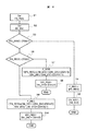
必要に応じて可変分周数Nの値を変化させるために、周波数設定レジスタF_REG、初期周波数設定レジスタFS_REG、第1及び第2の切り替え周波数レジスタFSW1及びFSW2、第1及び第2の切り替え値設定レジスタDDIV1及びDDIV2、初期IF分周比設定レジスタINI_DIV、IF分周比設定レジスタDIV_REGを用いる。動作は、図4に示すように以下の手順で行う。 In order to change the value of the variable frequency division number N as necessary, the frequency setting register F_REG, the initial frequency setting register FS_REG, the first and second switching frequency registers FSW1 and FSW2, and the first and second switching value settings The registers DDIV1 and DDIV2, the initial IF division ratio setting register INI_DIV, and the IF division ratio setting register DIV_REG are used. The operation is performed according to the following procedure as shown in FIG.
まず、ステップS1では、初期周波数設定レジスタFS_REGのデータ設定を行う。
ステップS2では、初期IF分周比設定レジスタINI_DIVのデータ設定を行う。
ステップS3では、初期周波数設定レジスタFS_REGの設定データと第1の切り替え周波数レジスタFSW1とのデータの比較を行い、真ならステップS6を、偽ならステップS4を実行する。
First, in step S1, data is set in the initial frequency setting register FS_REG.
In step S2, data is set in the initial IF division ratio setting register INI_DIV.
In step S3, the setting data in the initial frequency setting register FS_REG is compared with the data in the first switching frequency register FSW1, and if true, step S6 is executed, and if false, step S4 is executed.
ステップS4では、初期周波数設定レジスタFS_REGのデータを、周波数設定レジスタF_REGに格納する。
続いてステップS5に進み、初期IF分周比設定レジスタINI_DIVのデータを、IF分周比設定レジスタDIV_REGに格納して動作を終了する。
In step S4, the data of the initial frequency setting register FS_REG is stored in the frequency setting register F_REG.
In step S5, data in the initial IF division ratio setting register INI_DIV is stored in the IF division ratio setting register DIV_REG, and the operation ends.
ステップS6へ進んだ場合は、初期周波数設定レジスタFS_REGの設定データと第2の切り替え周波数レジスタFSW2のデータとの比較を行い、真ならステップS9を、偽ならステップS7を実行する。 When the process proceeds to step S6, the setting data of the initial frequency setting register FS_REG and the data of the second switching frequency register FSW2 are compared, and if true, step S9 is executed, and if false, step S7 is executed.
ステップS7では、周波数設定レジスタF_REGに、演算結果を格納する。
次に、ステップS8では、IF分周比設定レジスタDIV_REGに、初期IF分周比設定レジスタINI_DIVのデータと、第1の切り替え値設定レジスタDDIV1のデータとの和を格納して動作を終了する。
In step S7, the calculation result is stored in the frequency setting register F_REG.
Next, in step S8, the sum of the data in the initial IF division ratio setting register INI_DIV and the data in the first switching value setting register DDIV1 is stored in the IF division ratio setting register DIV_REG, and the operation ends.
ステップS9では、周波数設定レジスタF_REGに、演算結果を格納する。
ステップS10では、IF分周比設定レジスタDIV_REGに、初期IF分周比設定レジスタINI_DIVのデータと、第2の切り替え値設定レジスタDDIV2のデータとの和を格納して動作を終了する。
In step S9, the calculation result is stored in the frequency setting register F_REG.
In step S10, the sum of the data of the initial IF division ratio setting register INI_DIV and the data of the second switching value setting register DDIV2 is stored in the IF division ratio setting register DIV_REG, and the operation is ended.
ここで示した動作は一例であり、本発明の本質は、IF局部発振信号発生用の分周器の分周数を可変することにある。 The operation shown here is an example, and the essence of the present invention is to vary the frequency division number of the frequency divider for generating the IF local oscillation signal.
本発明の第2の実施例について、図5および図6を用いて説明する。本実施例は、第1の実施例において制御回路26内で行っていた図4に示した演算を、ベースバンドLSI(BBLSI)59で行う場合の例である。
A second embodiment of the present invention will be described with reference to FIGS. In this embodiment, the operation shown in FIG. 4 performed in the
図5は、第1の実施例の図3に対応する図であり、同じ構成部分には同じ参照符号を付して、その重複説明を省略する。本実施例では、図3の構成と異なり、制御回路26内にIF分周比設定レジスタDIV_REGが設けられ、代わりに制御回路26内にあった初期周波数設定レジスタFS_REG、第1及び第2の切り替え周波数レジスタFSW1,FSW2、第1及び第2の切り替え値設定レジスタDDIV1,DDIV2、および初期IF分周比設定レジスタINI_DIVが無い。
FIG. 5 is a diagram corresponding to FIG. 3 of the first embodiment, and the same components are denoted by the same reference numerals, and redundant description thereof is omitted. In this embodiment, unlike the configuration of FIG. 3, an IF frequency division ratio setting register DIV_REG is provided in the
図6は、RFIC34とBBLSI59との間での制御データの受け渡しを示す図である。RFIC34とBBLSI59との伝送のために、RFIC34にはデータ格納主レジスタMREGと個別データ格納レジスタPREG61が設けられている。データ格納主レジスタMREGには、BBLSI59から、クロック信号CLK、データDT、イネーブル信号ENが伝送される。
FIG. 6 is a diagram illustrating the transfer of control data between the
BBLSI59では、周波数設定レジスタF_REGと、IF分周比設定レジスタDIV_REGの内容を演算した後、得られた制御データをRFIC34に伝送する。伝送されてきたデータDTは、データ格納主レジスタMREGが、BBLSI59からのEN信号が発呼された時点で、個別データ格納レジスタPREG61に格納する。図5に示した制御回路26内の周波数設定レジスタF_REGと、IF分周比設定レジスタDIV_REGは、各々この個別データ格納レジスタ61の1つである。
The
制御データDTには、個別データレジスタの番号を登録するアドレス領域ADDと、書き込むデータが格納された領域DATがあり、シリアル伝送でBBLSI59から送られる。本実施例では、IF局部発振信号発生用分周器の分周数切り替えをプログラムで実行できるため、アルゴリズムに対する自由度が増す。
The control data DT includes an address area ADD for registering individual data register numbers and an area DAT in which data to be written is stored, and is sent from the
第3の実施例では、シンセサイザSS内の可変分周器22の分周数をΣΔ変調器を用いて制御する場合に好適なVCOのキャリブレーション方法について、図7〜12を用いて説明する。
In the third embodiment, a VCO calibration method suitable for controlling the frequency division number of the
本実施例では、図7に示す構成のVCOを用いる。このVCOは、電源75から電流源76で制御されるPMOSFET77a,77bを用いた正帰還形の発振器である。制御電圧は端子84に印加し、可変バイアス容量78a,78bを制御する。PMOSFET77a,77b、容量78a,78b、79a,79b、バイアス電流量、インダクタ82a,82bのバラツキによる発振周波数のズレを、k個の端子81−1〜81−kのバイアスを制御する事により、複数の容量79a,79b間に各々接続されるスイッチ80をオンオフさせて制御する。なお、端子83a,83bは、差動出力端子である。また、素子の参照番号に付いている添え字a,bは、理想的には特性が揃った対の素子であることを示している。
In this embodiment, a VCO having the configuration shown in FIG. 7 is used. This VCO is a positive feedback
この制御は、図8に示す回路により実行される。一定バイアス発生回路64の出力を、スイッチ65を切り替え、ループフィルタ25を介してVCO21のバイアス制御端子に印加する。すなわち、キャリブレーションできるように、位相同期ループを開ループにする。そして、シンセサイザで使用していた可変分周器22の出力がリファレンス信号fREF(26MHz)と一致するように、分周比設定レジスタ42内の1次(1st)と3次(3rd)のΣΔ変調器70,71用のΣΔ入力データレジスタCON_REGFと、リファレンス周波数倍周波数設定レジスタCON_REGIとを設定する。ここで、リファレンス周波数倍周波数設定レジスタCON_REGIは、可変分周器22の整数倍の分周数を設定するレジスタであり、例えばfREF=26MHzの整数倍の分周数が格納される。一方、ΣΔ入力データレジスタCON_REGFは上記整数倍以外の周波数ピッチを設定するレジスタであり、例えば100kHzピッチの数値が設定され、1次のΣΔ変調器70または3次のΣΔ変調器71を介して先のリファレンス周波数倍周波数設定レジスタCON_REGIの設定値と加算器73で加算されて可変分周器22の分周数を設定する。1次のΣΔ変調器70と3次のΣΔ変調器71との選択切り替えは、スイッチ72により行う。
This control is executed by the circuit shown in FIG. The output of the constant
VCOのキャリブレーションは、具体的には、破線で示す経路で行われる。先ず、スイッチ66によりループフィルタ25を一定バイアス発生回路64に接続してPLLループから切り離し、開ループにした後、可変分周器22の出力と、リファレンス周波数fREFとを、それぞれ例えば65分周の分周器DiV65A,DiV65Bにより分周して400kHzの信号とし、速度比較器FSDETを用いてどちらが先にカウントを終了するかを観測する。
Specifically, the calibration of the VCO is performed along a path indicated by a broken line. First, the
そして、そのカウント値の差分がゼロとなるように、すなわち図8に示したVCO内の容量78a,78bが設定バイアス条件でのバラツキに応じた容量値となるように、ΣΔ入力データレジスタCON_REGFとリファレンス周波数倍周波数設定レジスタCON_REGIの設定を行う。VCOバンド切り替え回路(VCO Band)69により、これらのレジスタの設定に応じた容量値となるよう図7に示したVCOのスイッチ80を切り替えて、設定された制御電圧、すなわちキャリブレーションされた電圧をVCO21の制御端子に印加する。この後は、スイッチ65を切り替えてループフィルタ25をチャージポンプ24に接続、すなわち閉ループにしてキャリブレーションが終了し、PLL制御による安定したVCO発振動作を続ける。この場合、ΣΔ変調器を用いると、次に説明するような誤差が発生する。
Then, the ΣΔ input data register CON_REGF is set so that the difference between the count values becomes zero, that is, the
図9に1次のΣΔ変調器を、図10に3次のΣΔ変調器の構成を示す。1次のΣΔ変調器86は、遅延器(D)、1ビット量子化器(Q)、増幅器(G)減算器93から構成される。
FIG. 9 shows the configuration of a first-order ΣΔ modulator, and FIG. 10 shows the configuration of a third-order ΣΔ modulator. The
このように構成される1次のΣΔ変調器70は、次のように動作する。入力端子85から入力された固定入力の10ビットのデジタル信号は、遅延器90に入力され、この遅延器90の出力結果と、前回入力された遅延器90の出力を量子化器91で1ビット量子化された結果を増幅器92で増幅されたものと減算器93で差を取り、その差を加算器89で入力端子に入力された信号に加算したものを再び遅延器に加え、遅延器の出力結果を先ほどと同様に量子化器で量子化し1ビットの信号を作り、増幅して帰還をかける。この一連の動作を繰り返し行うと、入力端子85で入力された数値を平均的に与えるようなデータ列(時変信号)が端子97より出力される。
The
また、3次のΣΔ変調器は、同様の構成の1次のΣΔ変調器86,87,88と微分器94,95とを用い、1次のΣΔ変調器86,87,88が直列に接続されると共に、3段目のΣΔ変調器88の出力を微分器95を介した出力と、1個の遅延器を介した2段目のΣΔ変調器87の出力とを加算した出力を、更に微分器94を介して、2個の遅延器を介した初段のΣΔ変調器86の出力に加算する構成となっている。
The third-order ΣΔ modulator uses first-
このように構成される3次のΣΔ変調器71は、次のように動作する。各段のΣΔ変調器の基本的動作は1次のΣΔ変調器と同じであるが、1段目は固定された入力で図9と同じ動作を行い、2段目、3段目のΣΔ変調器87,88は入力信号が固定でなく2段目のΣΔ変調器87は1段目のΣΔ変調器86の誤差が入力となり、3段目は2段目の誤差が入力となっている。ΣΔ変調器自身は積分器の特性を持っているので、3段目のΣΔ変調器88の出力を微分器95を介して元に戻し2段目の出力と加算し、この加算した出力をさらに微分器94でを介して元に戻して1段目の出力と加算して端子96から4ビットのデータ列が出力される。加算時のタイミングを合わせるために1段目のΣΔ変調器86には遅延器が2個、2段目のΣΔ変調器87の出力には遅延器1個それぞれ設けられている。
The third-
1次のΣΔ変調器の場合は、出力では1回の動作での誤差が±0.5(1ビット)の範囲であるが、3次のΣΔ変調器の場合は、出力では誤差が±7(4ビット)であり、次数が低いほうが望ましいのが理解される。このため、図7の構成においては、スイッチ72を切り替えて、シンセサイザ動作を行う場合には、図10に示す3次のΣΔ変調器71を選択し、キャリブレーション時には1次のΣΔ変調器70を選択する。
In the case of the first-order ΣΔ modulator, the error in one operation is in the range of ± 0.5 (1 bit) at the output, but in the case of the third-order ΣΔ modulator, the error is ± 7 in the output. It is understood that (4 bits) and a lower order is desirable. Therefore, in the configuration of FIG. 7, when the synthesizer operation is performed by switching the
図11に、VCOが890.2MHzの局部発振条件で、1次のΣΔ変調器を用いる場合の誤差を示す。図11は、2.5μsの期間の26MHzリファレンス周波数fREFと、890.2MHzのVCO21の発振周波数、および可変分周器22の出力DIVOUTを示している。図11において、四角で囲まれた数字は周期数を示し、2.5μsはfRFでは65周期(以下、ここでは、周期を「クロック」と呼ぶ)、VCOでは2225.5クロックとなるが、1次のΣΔ変調器70を用いた場合の65分周器(DiV65B)の出力DVOUTは、2225.5±0.5クロックとなり、VCOの発振周器で±0.5クロックの誤差があることが分かる。
FIG. 11 shows an error when a first-order ΣΔ modulator is used under a local oscillation condition where the VCO is 890.2 MHz. FIG. 11 shows the 26 MHz reference frequency fREF in the period of 2.5 μs, the oscillation frequency of the
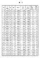
図12に他の主要周波数での計算結果を示す。図12において、CHはGMSのチャネル番号、fは周波数[MHz]、Niはリファレンス周波数倍周波数設定レジスタCON_REGIのレジスタ値、NfはΣΔ変調器入力データレジスタCON_REGFのレジスタ値、THEOは理論値[クロック]、ΣΔ(min)は1次のΣΔ変調器の最小値、ΣΔ(max)は1次のΣΔ変調器の最大値、TMERR(max)はタイミングエラーの最大値[クロック]、TMERR(min)はタイミングエラーの最小値[クロック]である。図12より、全て±0.5クロックである事が確認されている。 FIG. 12 shows the calculation results at other main frequencies. In FIG. 12, CH is the channel number of GMS, f is the frequency [MHz], Ni is the register value of the reference frequency double frequency setting register CON_REGI, Nf is the register value of the ΣΔ modulator input data register CON_REGF, and THEO is the theoretical value [clock. ], ΣΔ (min) is the minimum value of the first-order ΣΔ modulator, ΣΔ (max) is the maximum value of the first-order ΣΔ modulator, TMERR (max) is the maximum value of the timing error [clock], TMERR (min) Is the minimum timing error [clock]. From FIG. 12, it is confirmed that all are ± 0.5 clocks.
本実施例では、図13〜図17を用いてΣΔ変調器の固定スプリアスを低減するために疑似乱数を加える場合について述べる。図13は本実施例で用いる3次のΣΔ変調器である。図10に示した3次のΣΔ変調器と同じ構成部部には同じ参照符号を付して、その重複説明を省略する。すなわち、本実施例では3次のΣΔ変調器の入力に加算器98を設けて疑似乱数発生器100の出力を、直流成分をカットするための微分器99を介して印加する構成としている点が図10の構成と相違する。
In this embodiment, a case where a pseudo random number is added to reduce the fixed spurious of the ΣΔ modulator will be described with reference to FIGS. FIG. 13 shows a third-order ΣΔ modulator used in this embodiment. The same components as those of the third-order ΣΔ modulator shown in FIG. 10 are denoted by the same reference numerals, and redundant description thereof is omitted. That is, in this embodiment, an
ここで重要なのは、直流成分を無くして周波数誤差を発生させない事にある。疑似乱数発生器100の構成例を図14に示す。15個の遅延器101と、3個の排他的論理和102で構成されるPN15と呼ばれる疑似乱数発生器である。図15に示すように、異なる遅延器の出力の論理積(AND)103を取る事により、1の発生確率を制御し、雑音電力を例えば4分の1にすることが出来る。
What is important here is that the DC component is eliminated and no frequency error is generated. A configuration example of the pseudo
また図16に示すように、疑似乱数発生器100の出力を、ΣΔ変調器の2次部分に加算器104、または加算器105(点線の丸で表示)を設けて印加する事により、図13の微分器99を省略する事も出来る。図17に、スペクトルアナライザの表示をリファレンスバンド幅RBW=30kHzとして、GSM用チャネル番号95のシミュレーション結果の特性線を示す。縦軸はスペクトル強度SP(dB)であり、横軸は周波数f(kHz)である。特性線106は疑似乱数を印加しない図10の構成の場合であり、スプリアスが見られる。これに対して、疑似乱数を印加する図13の回路構成の場合の特性線107と、図16の回路構成の場合の特性線108に見られるように、スプリアスが抑圧されている事が分かる。
Also, as shown in FIG. 16, the output of the pseudo
本実施例では、ΣΔ変調器の内蔵ループフィルタが受けるパッケージの影響について述べる。図18Aは、VCO21、可変分周器22、位相比較器23、チャージポンプ回路24、ループフィルタ25で構成されるシンセサイザであり、ループフィルタ25は容量C1と抵抗R1の直列接続回路と容量C2との並列接続で構成されるラグリードフィルタ109とR2と容量C3からなる低域通過フィルタ110で構成される。同図において、Kv/SはVCO21の伝達関数を、1/nは可変分周器22の分周数を表わしている。
In this embodiment, the influence of the package on the built-in loop filter of the ΣΔ modulator will be described. FIG. 18A shows a synthesizer including a
また、本実施例では1次の低域通過フィルタを用いた場合を示しているが、1次以上の低域通過フィルタを用いても良いことは勿論である。 Moreover, although the case where a primary low-pass filter is used is shown in the present embodiment, it goes without saying that a primary or higher-order low-pass filter may be used.
図18Aは理想的な接地が取れた場合であり、図18Bは1箇所で共通して接地する場合、図18Cはラグリードフィルタ109と、低域通過フィルタ110とを分けて接地した場合、すなわちラグリードフィルタ109の接地をチャージポンプ24の接地端子に接続し、低域通過フィルタ110の接地をVCO21の接地端子に接続した場合であり、図18Dはループフィルタを全てパッケージの外に取り付けた場合である。なお、図18B〜Dではパッケージの寄生インダクタLpを加えてある。
18A shows a case where ideal grounding is achieved, FIG. 18B shows a case where grounding is common at one location, and FIG. 18C shows a case where the
図19は、図18A〜Dの接地形態に応じた利得の周波数特性を示す図であり、図中A〜Dは、それぞれ図18A〜Dに対応する。図19において、縦軸は利得GA(dB)、横軸は周波数f(Hz)である。図19より、図18B,図18Dの接地形態の場合はパッケージのインダクタLpの影響で減衰効果に制限がかかるが、図18Cのように接地を分離することで制限を低減できることが分かる。 FIG. 19 is a diagram illustrating frequency characteristics of gains according to the grounding configurations of FIGS. 18A to 18D, where A to D correspond to FIGS. 18A to 18D, respectively. In FIG. 19, the vertical axis represents gain GA (dB), and the horizontal axis represents frequency f (Hz). From FIG. 19, it can be seen that in the case of the ground configuration shown in FIGS. 18B and 18D, the attenuation effect is limited by the influence of the inductor Lp of the package, but the limitation can be reduced by separating the ground as shown in FIG. 18C.
これまでの実施例では、オフセットPLLを主に説明したが、本実施例は図20に示すように、本発明を2ステップ送信機に適用した場合である。ここでは、図3に示した回路構成を適用している。図3と同じ構成部分には、同じ参照符号を付して、重複する説明は省略する。すなわち、本実施例では、図3のオフセットPLL部O−PLLの代わりに、送信周波数帯TXを、送信ミキサ112、RF帯域通過フィルタ113、IF帯域通過フィルタ114で構成している点が相違する。本実施例でも図3の回路と同様に、受信回路の局部発振用として用いてきたシンセサイザSS内のVCO21を、送信用RFローカル信号、直交変調器8を駆動するIFローカル信号を生成している。
In the embodiments so far, the offset PLL has been mainly described, but this embodiment is a case where the present invention is applied to a two-step transmitter as shown in FIG. Here, the circuit configuration shown in FIG. 3 is applied. The same components as those in FIG. 3 are denoted by the same reference numerals, and redundant description is omitted. That is, the present embodiment is different in that the transmission frequency band TX is configured by a
直交変調器の出力は、IF帯域通過フィルタ114を介してミキサ112の一方の入力に、他方のミキサの入力には制御回路26により制御されてVCO21から分周して生成されたRFローカル信号が入力される。ミキサ112の出力はRF帯域通過フィルタ113を介して送信周波数帯信号が生成される。、図2に示したような送信スプリアスを回避する動作を行うことは勿論であり、VCOの共用化により小型化も図れる。
The output of the quadrature modulator is supplied to one input of the
以上、本発明の好適な実施例について欧州向け携帯電話を中心に説明したが、上記実施例に限定されるものではなく、本発明の精神を逸脱しない範囲内において、種々の設計変更をなし得ることは言うまでもない。例えば、本発明はCDMA等他の携帯電話、無線LAN等にも適用できることは勿論である。 The preferred embodiments of the present invention have been described above mainly with respect to mobile phones for Europe. However, the present invention is not limited to the above-described embodiments, and various design changes can be made without departing from the spirit of the present invention. Needless to say. For example, the present invention can be applied to other mobile phones such as CDMA, wireless LAN, and the like.
1…バンドパスフィルタ(BPF)、2…低雑音増幅器(LNA)、3,16…ミキサ、4,9,27,29,31,32…1/2分周器、5…可変増幅器・フィルタ列(PGA/LPF)、6…アッテネータ、7…低域通過フィルタ、8…直交変調器、10…リミッタ、11…位相比較器(PD)、12,25…ループフィルタ(LF)、13…送信用発振器、14…1/4分周器、15…1/2分周器、17…GSM/GSM850用電力増幅器、18…DCS/PCS用電力増幅器、19,20…送信用低域通過フィルタ(LPF)、21…スイッチ、22…可変分周器、23…位相比較器、24…チャージポンプ回路、26…制御回路(CONT)、28,33…切り替えスイッチ、30…可変分周器(IFDIV)、34…RFIC、42…分周比設定レジスタ(CON_REG)、43…シグマデルタ(ΣΔ)変調器、44…加算器、59…ベースバンドLSI(BBLSI)、61…個別データ格納用レジスタ(PREG)、64…一定バイアス回路、66…切り替えスイッチ、68…速度比較器(FSDET)、69…VCOバンド切り替え回路(VCOBand)、70…1次ΣΔ変調器、71…3次ΣΔ変調器、72…切り替えスイッチ、75…電源、76…電流源、77a,77b…PMOSFET、78a,78b…バイアス可変容量、79a,79b…容量、80…スイッチ、81−1〜81−k…スイッチ制御端子、82…インダクタ、83…出力、84…バイアス制御端子、84…スイッチ切り替え端子、85…入力端子、86,87,88…1次ΣΔ変調器、89…加算器、90…遅延器、91…量子化器、92…増幅器、93…減算器、94,95…微分器、96,97…出力端子、98…加算器、99…直流除去手段(微分器)、100…疑似乱数発生器、101…遅延器、102…排他的論理和(EOR)、103…論理積(AND)、104…加算器、105…加算器挿入位置、106…ΣΔ変調器出力、107…図13の出力波形、108…図16の出力波形、109…ラグリード形フィルタ、110…低域通過フィルタ、112…送信ミキサ、113…RF帯域通過フィルタ、114…IF帯域通過フィルタ、FSW1…第1切り替え周波数レジスタ、FSW2…第2切り替え周波数レジスタ、FS_REG…初期周波数設定レジスタ、DDIV1…第1切り替え値設定レジスタ、DDIV2…第2切り替え値設定レジスタ、F_REG…周波数設定レジスタ、INI_DIV…初期IF分周比設定レジスタ、DIV_REG…IF分周比設定レジスタ、MREG…データ格納用主レジスタ、DT…制御データ、ADD…アドレス領域と、DAT…データ格納領域、CON_REGF…ΣΔ変調器入力データレジスタ、CON_REG…リファレンス周波数倍周波数設定レジスタ、DiV65A,DiV65B…分周器、Lp…寄生インダクタ。
DESCRIPTION OF
Claims (9)
第1の周波数変換回路と、
前記第1の周波数変換回路の出力が入力される第2の周波数変換回路と、
第1の分周回路部とを具備し、
前記第1の周波数発生回路の出力が、前記第1の分周回路部を介して前記第1の周波数変換回路の局部発振信号として供給され、
前記第1の周波数発生回路の出力が、直接または第2の分周回路部を介して前記第2の周波数変換回路の局部発振信号として供給され、
前記第1の分周回路部の分周数が、可変に設定されて成ることを特徴とする無線送信回路。 A first frequency generation circuit;
A first frequency conversion circuit;
A second frequency conversion circuit to which an output of the first frequency conversion circuit is input;
A first frequency divider circuit;
The output of the first frequency generation circuit is supplied as a local oscillation signal of the first frequency conversion circuit via the first frequency dividing circuit unit,
The output of the first frequency generation circuit is supplied as a local oscillation signal of the second frequency conversion circuit directly or via a second frequency divider circuit unit,
The wireless transmission circuit according to claim 1, wherein the frequency dividing number of the first frequency dividing circuit section is variably set.
前記第1の周波数変換回路は直交変調器であり、
前記第1の分周回路部の分周数が偶数に設定されることによって前記直交変調器に入力される90度位相の異なる2つの局部発振信号が発生されることを特徴とする無線送信回路。 The wireless transmission circuit according to claim 1,
The first frequency conversion circuit is a quadrature modulator;
A radio transmission circuit characterized in that two local oscillation signals having a phase difference of 90 degrees inputted to the quadrature modulator are generated by setting the frequency division number of the first frequency divider circuit unit to an even number. .
前記第2の周波数変換回路は、
第1および第2の入力端子を有する第1の位相比較回路と、
前記第1の位相比較回路の出力が入力される第1のループフィルタ回路と、
前記第1のループフィルタ回路の出力が電圧制御端子に接続される第1の電圧制御発振器と、
前記第1の電圧制御発振器の出力が入力される第1のミキサ回路とを具備し、
前記第1のループフィルタ回路の入力には前記第1の位相比較回路の出力が接続され、
前記第1の位相比較回路の前記第2の入力端子には前記第1のミキサ回路の出力が接続されて成り、
前記第2の周波数変換回路の入力は前記第1の位相比較回路の第1の入力端子であることを特徴とする無線送信回路。 The wireless transmission circuit according to claim 2,
The second frequency conversion circuit includes:
A first phase comparison circuit having first and second input terminals;
A first loop filter circuit to which an output of the first phase comparison circuit is input;
A first voltage controlled oscillator in which an output of the first loop filter circuit is connected to a voltage control terminal;
A first mixer circuit to which the output of the first voltage controlled oscillator is input,
The output of the first phase comparison circuit is connected to the input of the first loop filter circuit,
An output of the first mixer circuit is connected to the second input terminal of the first phase comparison circuit;
The wireless transmission circuit, wherein an input of the second frequency conversion circuit is a first input terminal of the first phase comparison circuit.
前記第1の周波数発生回路は、第2の電圧制御発振器と、第2の可変分周器と、第2の位相比較回路と、チャージポンプ回路と、第2のループフィルタ回路とを含む位相同期ループ回路で構成されて成り、
前記第2の可変分周器の分周数が時変であるフラクショナル型位相同期ループ発振回路であることを特徴とする無線送信回路。 The wireless transmission circuit according to any one of claims 1 to 3,
The first frequency generation circuit includes a second voltage controlled oscillator, a second variable frequency divider, a second phase comparison circuit, a charge pump circuit, and a second loop filter circuit. It consists of a loop circuit,
A wireless transmission circuit, wherein the second variable frequency divider is a fractional phase-locked loop oscillation circuit in which the frequency division number is time-varying.
前記第1の周波数発生回路は、
前記第2の電圧制御発振器の電圧制御入力に固定電位を与えるバイアス部と、
前記第2の電圧制御発振器の共振周波数を切り替える切り替え部と、
第1の基準信号路で駆動される第1のカウンタ回路と、
前記第2の可変分周器の出力に設けられた第2のカウンタ回路と、
前記第1および第2のカウンタ回路間のカウント時間の差に応じて前記共振周波数の切り替え部の選択を決定する回路部と、
前記第2の可変分周器の分周数を制御する第1のシグマデルタ変調器と、
前記第1のシグマデルタ変調器よりも次数の大きい第2のシグマデルタ変調器とを更に具備し、
前記第1の周波数発生回路が位相同期ループ動作の時には、前記第1のシグマデルタ変調器が用いられ、
前記第1の周波数発生回路がキャリブレーション動作の時には、前記第2のシグマデルタ変調器が用いられることを特徴とする無線送信回路。 The wireless transmission circuit according to claim 4, wherein
The first frequency generation circuit includes:
A bias unit for applying a fixed potential to a voltage control input of the second voltage controlled oscillator;
A switching unit for switching a resonance frequency of the second voltage controlled oscillator;
A first counter circuit driven by a first reference signal path;
A second counter circuit provided at the output of the second variable frequency divider;
A circuit unit that determines selection of the switching unit of the resonance frequency according to a difference in count time between the first and second counter circuits;
A first sigma delta modulator for controlling a frequency division number of the second variable frequency divider;
A second sigma delta modulator having a higher order than the first sigma delta modulator;
When the first frequency generation circuit is in a phase-locked loop operation, the first sigma delta modulator is used,
The wireless transmission circuit, wherein the second sigma delta modulator is used when the first frequency generation circuit is in a calibration operation.
前記位相同期ループ回路内の前記第2の可変分周器の分周比の設定は、
第1のシグマデルタ変調器と、
第1の加算器と、
第2の加算器と、
第1の周波数条件記憶部と、
第2の周波数条件記憶部と、
第1の疑似乱数発生回路とを具備する回路により行われ、
前記第1の加算器の出力が前記第2の可変分周器の分周比設定端子に接続され、
前記第1の加算器の、第1の入力端子が前記第1のシグマデルタ変調器の出力に、第2の入力端子が前記第1の周波数条件記憶部の所定の上位ビット列出力にそれぞれ接続され、
前記第1のシグマデルタ変調器の入力が前記第2の加算器の出力に接続され、
前記第2の加算器の第1の入力端子が前記第2の周波数条件記憶部の所定の下位ビット列出力に接続され、
前記第2の加算器の第2の入力端子が前記第1の疑似乱数発生回路に接続されて成り、
前記疑似乱数発生回路の出力が直流成分を発生しないことを特徴とする無線送信回路。 The wireless transmission circuit according to claim 4, wherein
Setting the frequency division ratio of the second variable frequency divider in the phase locked loop circuit is as follows:
A first sigma delta modulator;
A first adder;
A second adder;
A first frequency condition storage unit;
A second frequency condition storage unit;
A circuit comprising a first pseudo-random number generator,
An output of the first adder is connected to a frequency division ratio setting terminal of the second variable frequency divider;
A first input terminal of the first adder is connected to an output of the first sigma delta modulator, and a second input terminal is connected to a predetermined upper bit string output of the first frequency condition storage unit. ,
The input of the first sigma delta modulator is connected to the output of the second adder;
A first input terminal of the second adder is connected to a predetermined lower bit string output of the second frequency condition storage unit;
A second input terminal of the second adder is connected to the first pseudorandom number generation circuit;
A radio transmission circuit characterized in that the output of the pseudo-random number generation circuit does not generate a DC component.
前記第2の可変分周器の分周比を設定するための回路は、
第1のシグマデルタ変調器と、
第1の加算器と、
第1の周波数条件記憶部と、
第2の周波数条件記憶部と、
第1の疑似乱数発生回路と
第1および第2の微分器とを含んで成り、
前記第1の加算器の出力が前記第2の可変分周器の分周比設定端子に接続され、
前記第1の加算器の、第1の入力端子が前記第1のシグマデルタ変調器の出力に、第2の入力端子が前記第1の周波数条件記憶部の所定の上位ビット列出力にそれぞれ接続され、
前記第1のシグマデルタ変調器の入力が前記第2の周波数条件記憶部の所定の下位ビット列出力に接続され、
前記第1のシグマデルタ変調器が、入力端子、出力端子、誤差出力端子をそれぞれ持つ第1、第2、第3の1次のシグマデルタ変調器を具備して成り、
前記第1の1次のシグマデルタ変調器の誤差出力が前記第2の1次シグマデルタ変調器の入力に接続され、
前記第2の1次シグマデルタ変調器の出力が前記第1の微分器を介して前記第1の1次のシグマデルタ変調器の出力に接続され、
前記第2の1次のシグマデルタ変調器の誤差出力が前記第3の1次シグマデルタ変調器の入力に接続され、
前記第3の1次シグマデルタ変調器の出力が前記第2の微分器を介して前記第2の1次のシグマデルタ変調器の出力に接続され、
前記第1の疑似乱数発生回路の出力が前記第1の1次のシグマデルタ変調器の誤差出力に加算されて前記第2の1次シグマデルタ変調器に入力される構成であることを特徴とする無線送信回路。 The transmission circuit according to claim 4, wherein
A circuit for setting a frequency division ratio of the second variable frequency divider is:
A first sigma delta modulator;
A first adder;
A first frequency condition storage unit;
A second frequency condition storage unit;
Comprising a first pseudo-random number generation circuit and first and second differentiators;
An output of the first adder is connected to a frequency division ratio setting terminal of the second variable frequency divider;
A first input terminal of the first adder is connected to an output of the first sigma-delta modulator, and a second input terminal is connected to a predetermined upper bit string output of the first frequency condition storage unit. ,
An input of the first sigma delta modulator is connected to a predetermined lower bit string output of the second frequency condition storage unit;
The first sigma delta modulator comprises first, second and third primary sigma delta modulators each having an input terminal, an output terminal and an error output terminal;
An error output of the first primary sigma delta modulator is connected to an input of the second primary sigma delta modulator;
The output of the second first order sigma delta modulator is connected to the output of the first first order sigma delta modulator via the first differentiator;
An error output of the second primary sigma delta modulator is connected to an input of the third primary sigma delta modulator;
The output of the third first order sigma delta modulator is connected to the output of the second first order sigma delta modulator via the second differentiator;
The output of the first pseudo random number generation circuit is added to the error output of the first primary sigma delta modulator and input to the second primary sigma delta modulator. Wireless transmission circuit.
前記第2のループフィルタが、少なくとも第1の容量と第1の抵抗で構成される第1の直列接続回路と第2の容量との並列接続で構成される第1のラグリードフィルタと、1次以上の第1の低域通過フィルタとで構成され、
前記チャージポンプ回路の出力は前記第1のラグリードフィルタの第1の端子と前記第1の低域通過フィルタの入力端子とに接続され、
前記第1のラグリードフィルタの第2の端子が前記チャージポンプ回路の接地端子に接続され、
前記第1の低域通過フィルタの出力端子が前記第2の電圧制御発振器の電圧制御端子に、接地端子が前記第2の電圧制御発振器の接地端子にそれぞれ接続されることを特徴とする無線送信回路。 The transmission circuit according to claim 4, wherein
A first lag reed filter configured by a parallel connection of a first series connection circuit including at least a first capacitor and a first resistor and a second capacitor; A first or higher first low-pass filter,
An output of the charge pump circuit is connected to a first terminal of the first lag-lead filter and an input terminal of the first low-pass filter;
A second terminal of the first lug reed filter is connected to a ground terminal of the charge pump circuit;
The radio transmission characterized in that an output terminal of the first low-pass filter is connected to a voltage control terminal of the second voltage controlled oscillator, and a ground terminal is connected to a ground terminal of the second voltage controlled oscillator. circuit.
アンテナで受信した信号を妨害波を除去するフィルタ回路を介して低雑音増幅器により増幅した後、ベースバンド信号に周波数変換してベースバンド部へ送る受信回路部とを備えた送受信機であって、
前記無線送信回路部に、請求項1に記載の無線送信回路を用いたことを特徴とする送受信機。
A wireless transmission circuit unit for transmitting a transmission signal from the baseband processing unit via an antenna;
A transceiver having a receiving circuit unit that amplifies a signal received by an antenna by a low noise amplifier through a filter circuit that removes interference waves, and then converts the frequency to a baseband signal and sends it to the baseband unit,
A transceiver using the wireless transmission circuit according to claim 1 for the wireless transmission circuit unit.
Priority Applications (4)
| Application Number | Priority Date | Filing Date | Title |
|---|---|---|---|
| JP2004184779A JP4327666B2 (en) | 2004-06-23 | 2004-06-23 | Wireless transmission circuit and transceiver using the same |
| CN200510078673XA CN1756093B (en) | 2004-06-23 | 2005-06-21 | Radio transmission circuit and transmitter-receiver employing the same |
| CN201110185923.5A CN102307049B (en) | 2004-06-23 | 2005-06-21 | Wireless transmitter circuit and transceiver using the same |
| US11/158,094 US8055218B2 (en) | 2004-06-23 | 2005-06-22 | Wireless transmitter circuit and transceiver using the same |
Applications Claiming Priority (1)
| Application Number | Priority Date | Filing Date | Title |
|---|---|---|---|
| JP2004184779A JP4327666B2 (en) | 2004-06-23 | 2004-06-23 | Wireless transmission circuit and transceiver using the same |
Related Child Applications (1)
| Application Number | Title | Priority Date | Filing Date |
|---|---|---|---|
| JP2009021328A Division JP2009105959A (en) | 2009-02-02 | 2009-02-02 | Radio transmission circuit and transmitter-receiver employing the same |
Publications (2)
| Publication Number | Publication Date |
|---|---|
| JP2006013674A true JP2006013674A (en) | 2006-01-12 |
| JP4327666B2 JP4327666B2 (en) | 2009-09-09 |
Family
ID=35506567
Family Applications (1)
| Application Number | Title | Priority Date | Filing Date |
|---|---|---|---|
| JP2004184779A Expired - Fee Related JP4327666B2 (en) | 2004-06-23 | 2004-06-23 | Wireless transmission circuit and transceiver using the same |
Country Status (3)
| Country | Link |
|---|---|
| US (1) | US8055218B2 (en) |
| JP (1) | JP4327666B2 (en) |
| CN (2) | CN102307049B (en) |
Cited By (3)
| Publication number | Priority date | Publication date | Assignee | Title |
|---|---|---|---|---|
| JP2007228244A (en) * | 2006-02-23 | 2007-09-06 | Matsushita Electric Ind Co Ltd | Transmitter |
| JP2007259122A (en) * | 2006-03-23 | 2007-10-04 | Renesas Technology Corp | Semiconductor integrated circuit for communication |
| JP2008131098A (en) * | 2006-11-16 | 2008-06-05 | Hitachi Media Electoronics Co Ltd | Multiband radio device and semiconductor integrated circuit |
Families Citing this family (15)
| Publication number | Priority date | Publication date | Assignee | Title |
|---|---|---|---|---|
| GB2424324B (en) * | 2005-03-14 | 2008-10-01 | Renesas Tech Corp | Communication semiconductor integrated circuit device incorporating a pll circuit therein |
| US7474880B2 (en) * | 2005-03-24 | 2009-01-06 | Broadcom Corporation | Linear and non-linear dual mode transmitter |
| US7183858B2 (en) * | 2005-03-31 | 2007-02-27 | Broadcom Corporation | Wireless transmitter having multiple programmable gain amplifiers (PGAs) with tuned impedance to provide substantially linear magnitude and phase responses |
| JP2007133527A (en) * | 2005-11-09 | 2007-05-31 | Fujifilm Corp | Clock signal generation circuit, semiconductor integrated circuit, and frequency-division rate control method |
| US7652604B2 (en) * | 2007-02-28 | 2010-01-26 | Exar Corporation | Programmable analog-to-digital converter for low-power DC-DC SMPS |
| US7995979B2 (en) * | 2008-03-04 | 2011-08-09 | Mediatek Inc. | Wireless receiver with automatic gain control and method for automatic gain control of receiving circuit utilized in wireless receiver |
| DE102008044744B4 (en) * | 2008-08-28 | 2015-05-21 | Intel Mobile Communications GmbH | Method and apparatus for noise shaping a transmission signal |
| US20100094995A1 (en) * | 2008-10-14 | 2010-04-15 | Entropic Communications, Inc. | Silent Probes in a Communication Network |
| US8418036B2 (en) * | 2008-10-16 | 2013-04-09 | Entropic Communications, Inc. | Method and apparatus for performing forward error correction in an orthogonal frequency division multiplexed communication network |
| US8363681B2 (en) * | 2008-10-16 | 2013-01-29 | Entropic Communications, Inc. | Method and apparatus for using ranging measurements in a multimedia home network |
| US8320566B2 (en) * | 2008-10-16 | 2012-11-27 | Entropic Communications, Inc. | Method and apparatus for performing constellation scrambling in a multimedia home network |
| CN101741788B (en) * | 2009-11-27 | 2012-10-03 | 许昌学院 | Method for modulating and demodulating minimum frequency shift keying signal and special method for designing complex analytic band-pass filter |
| CN104967198B (en) * | 2010-07-28 | 2018-08-14 | 株式会社半导体能源研究所 | Wireless power supply system and wireless power method |
| US9712226B2 (en) * | 2014-05-15 | 2017-07-18 | Qualcomm Incorporated | Multi-way diversity receiver with multiple synthesizers in a carrier aggregation transceiver |
| CN106656188B (en) * | 2016-12-30 | 2023-07-18 | 中国电子科技集团公司第四十三研究所 | High-precision zero offset adjustment R/D converter and implementation method thereof |
Family Cites Families (24)
| Publication number | Priority date | Publication date | Assignee | Title |
|---|---|---|---|---|
| JPH09261106A (en) * | 1996-03-22 | 1997-10-03 | Matsushita Electric Ind Co Ltd | Mobile radio equipment operated for plural frequency bands |
| JP3848445B2 (en) * | 1997-09-26 | 2006-11-22 | 松下電器産業株式会社 | Radio equipment compatible with multiple communication systems |
| JP3088368B2 (en) * | 1997-12-10 | 2000-09-18 | 静岡日本電気株式会社 | Direct conversion receiver |
| US6150890A (en) * | 1998-03-19 | 2000-11-21 | Conexant Systems, Inc. | Dual band transmitter for a cellular phone comprising a PLL |
| JP3369480B2 (en) * | 1998-07-31 | 2003-01-20 | 松下電器産業株式会社 | Wireless circuit device |
| US6181212B1 (en) * | 1999-01-28 | 2001-01-30 | Lucent Technologies, Inc. | Phase locked loop for generating two disparate, variable frequency signals |
| WO2001071934A1 (en) | 2000-03-21 | 2001-09-27 | Koninklijke Philips Electronics N.V. | Communication system with frequency modulation and with a single local oscillator |
| JP3461799B2 (en) | 2000-11-16 | 2003-10-27 | 松下電器産業株式会社 | Delta-sigma modulation type fractional frequency division PLL frequency synthesizer |
| JP2002208869A (en) * | 2001-01-09 | 2002-07-26 | Sony Corp | Multiband radio signal transmission/reception device |
| US6920182B2 (en) * | 2001-01-09 | 2005-07-19 | Microtune (Texas), L.P. | Delta-sigma modulator system and method |
| DE10108636A1 (en) * | 2001-02-22 | 2002-09-19 | Infineon Technologies Ag | Adjustment method and adjustment device for PLL circuit for two-point modulation |
| US6671500B2 (en) * | 2001-03-30 | 2003-12-30 | Skyworks Solutions, Inc. | Frequency plan |
| JP2004522361A (en) * | 2001-06-15 | 2004-07-22 | アナログ ディヴァイスィズ インク | Variable coefficient interpolator and variable frequency synthesizer incorporating variable coefficient interpolator |
| US6868261B2 (en) * | 2001-09-05 | 2005-03-15 | Broadcom Corporation | Transmitter method, apparatus, and frequency plan for minimizing spurious energy |
| JP2003318732A (en) * | 2002-04-26 | 2003-11-07 | Hitachi Ltd | Semiconductor integrated circuit for communication, and radio communication system |
| US6707855B2 (en) * | 2002-06-20 | 2004-03-16 | Nokia Corporation | Digital delta sigma modulator in a fractional-N frequency synthesizer |
| JP2004104228A (en) * | 2002-09-05 | 2004-04-02 | Matsushita Electric Ind Co Ltd | Signal processing apparatus and signal processing method, delta sigma modulation fractional frequency division pll frequency synthesizer, wireless communication apparatus, and delta sigma modulation digital/analog converter |
| TW578387B (en) * | 2002-10-31 | 2004-03-01 | Mediatek Inc | Phase-lock loop applying in wireless communication system and method thereof |
| EP1420523A1 (en) * | 2002-11-13 | 2004-05-19 | Asulab S.A. | Apparatus for wireless transmission of information and communication system comprising said apparatus |
| EP1427108A1 (en) * | 2002-12-03 | 2004-06-09 | Motorola, Inc. | A third order sigma-delta modulator for noise shaping in a phase locked loop and method thereof |
| DE10257181B3 (en) * | 2002-12-06 | 2004-07-15 | Infineon Technologies Ag | Phase locked loop with modulator |
| US6903585B2 (en) * | 2003-06-27 | 2005-06-07 | Analog Devices, Inc. | Pulse width modulated common mode feedback loop and method for differential charge pump |
| JP3830924B2 (en) * | 2003-07-04 | 2006-10-11 | 松下電器産業株式会社 | Cascaded delta-sigma modulator |
| US20050266805A1 (en) * | 2004-05-28 | 2005-12-01 | Jensen Henrik T | Digital delta sigma modulator and applications thereof |
-
2004
- 2004-06-23 JP JP2004184779A patent/JP4327666B2/en not_active Expired - Fee Related
-
2005
- 2005-06-21 CN CN201110185923.5A patent/CN102307049B/en not_active Expired - Fee Related
- 2005-06-21 CN CN200510078673XA patent/CN1756093B/en not_active Expired - Fee Related
- 2005-06-22 US US11/158,094 patent/US8055218B2/en active Active
Cited By (5)
| Publication number | Priority date | Publication date | Assignee | Title |
|---|---|---|---|---|
| JP2007228244A (en) * | 2006-02-23 | 2007-09-06 | Matsushita Electric Ind Co Ltd | Transmitter |
| JP2007259122A (en) * | 2006-03-23 | 2007-10-04 | Renesas Technology Corp | Semiconductor integrated circuit for communication |
| JP2008131098A (en) * | 2006-11-16 | 2008-06-05 | Hitachi Media Electoronics Co Ltd | Multiband radio device and semiconductor integrated circuit |
| JP4641021B2 (en) * | 2006-11-16 | 2011-03-02 | 株式会社日立メディアエレクトロニクス | Multiband radio and semiconductor integrated circuit |
| US7945232B2 (en) | 2006-11-16 | 2011-05-17 | Hitachi Media Electronics Co., Ltd. | Multiband wireless device and semiconductor integrated circuit |
Also Published As
| Publication number | Publication date |
|---|---|
| CN1756093B (en) | 2011-08-10 |
| CN102307049A (en) | 2012-01-04 |
| JP4327666B2 (en) | 2009-09-09 |
| US8055218B2 (en) | 2011-11-08 |
| US20050287964A1 (en) | 2005-12-29 |
| CN1756093A (en) | 2006-04-05 |
| CN102307049B (en) | 2014-06-25 |
Similar Documents
| Publication | Publication Date | Title |
|---|---|---|
| US8055218B2 (en) | Wireless transmitter circuit and transceiver using the same | |
| US8670737B2 (en) | Digital delta Sigma modulator and applications thereof | |
| JP5762980B2 (en) | Frequency synthesizer with multiple tuning loops | |
| JP5662911B2 (en) | High frequency signal processing apparatus and radio communication system | |
| US7324789B2 (en) | PLL frequency synthesizer architecture for low phase noise and reference spurs | |
| US9000815B2 (en) | Fractional spur reduction using controlled clock jitter | |
| JP4233082B2 (en) | Frequency synthesizer and mobile terminal device | |
| JP4214098B2 (en) | Sigma delta transmission circuit and transceiver using the same | |
| CN105577178B (en) | A kind of broadband low phase noise Sigma-Delta phaselocked loop | |
| US20060211381A1 (en) | RF transceiver incorporating dual-use PLL frequency synthesizer | |
| EP1458111B1 (en) | Multi-band frequency synthesizer | |
| WO2009152106A2 (en) | Dithering a digitally-controlled oscillator output in a phase-locked loop | |
| CN101090279A (en) | Wireless transceiver and its modulation path delay calibration method | |
| WO2008035260A1 (en) | Digital polar radiofrequency transmitting device with a radiofrequency reference oscillator and an integrated circuit comprising such device | |
| US7974333B2 (en) | Semiconductor apparatus and radio circuit apparatus using the same | |
| US9948450B2 (en) | Frequency generator | |
| US7653359B2 (en) | Techniques to decrease fractional spurs for wireless transceivers | |
| JP2009105959A (en) | Radio transmission circuit and transmitter-receiver employing the same | |
| KR101208041B1 (en) | Frequency synthesizer for wide range frequenct synthesization with compact size | |
| WO2014078311A2 (en) | Frequency synthesis using a phase locked loop | |
| GB2373113A (en) | Improvements in or relating to fast frequency-hopping synthesisers | |
| JP2005328385A (en) | Radio receiving device |
Legal Events
| Date | Code | Title | Description |
|---|---|---|---|
| A621 | Written request for application examination |
Free format text: JAPANESE INTERMEDIATE CODE: A621 Effective date: 20061027 |
|
| RD02 | Notification of acceptance of power of attorney |
Free format text: JAPANESE INTERMEDIATE CODE: A7422 Effective date: 20061027 |
|
| A977 | Report on retrieval |
Free format text: JAPANESE INTERMEDIATE CODE: A971007 Effective date: 20081120 |
|
| A131 | Notification of reasons for refusal |
Free format text: JAPANESE INTERMEDIATE CODE: A131 Effective date: 20081202 |
|
| A521 | Written amendment |
Free format text: JAPANESE INTERMEDIATE CODE: A523 Effective date: 20090202 |
|
| A131 | Notification of reasons for refusal |
Free format text: JAPANESE INTERMEDIATE CODE: A131 Effective date: 20090303 |
|
| A521 | Written amendment |
Free format text: JAPANESE INTERMEDIATE CODE: A523 Effective date: 20090421 |
|
| TRDD | Decision of grant or rejection written | ||
| A01 | Written decision to grant a patent or to grant a registration (utility model) |
Free format text: JAPANESE INTERMEDIATE CODE: A01 Effective date: 20090519 |
|
| A01 | Written decision to grant a patent or to grant a registration (utility model) |
Free format text: JAPANESE INTERMEDIATE CODE: A01 |
|
| A61 | First payment of annual fees (during grant procedure) |
Free format text: JAPANESE INTERMEDIATE CODE: A61 Effective date: 20090611 |
|
| FPAY | Renewal fee payment (event date is renewal date of database) |
Free format text: PAYMENT UNTIL: 20120619 Year of fee payment: 3 |
|
| R150 | Certificate of patent or registration of utility model |
Ref document number: 4327666 Country of ref document: JP Free format text: JAPANESE INTERMEDIATE CODE: R150 Free format text: JAPANESE INTERMEDIATE CODE: R150 |
|
| FPAY | Renewal fee payment (event date is renewal date of database) |
Free format text: PAYMENT UNTIL: 20120619 Year of fee payment: 3 |
|
| S111 | Request for change of ownership or part of ownership |
Free format text: JAPANESE INTERMEDIATE CODE: R313111 |
|
| FPAY | Renewal fee payment (event date is renewal date of database) |
Free format text: PAYMENT UNTIL: 20120619 Year of fee payment: 3 |
|
| R350 | Written notification of registration of transfer |
Free format text: JAPANESE INTERMEDIATE CODE: R350 |
|
| FPAY | Renewal fee payment (event date is renewal date of database) |
Free format text: PAYMENT UNTIL: 20120619 Year of fee payment: 3 |
|
| FPAY | Renewal fee payment (event date is renewal date of database) |
Free format text: PAYMENT UNTIL: 20130619 Year of fee payment: 4 |
|
| FPAY | Renewal fee payment (event date is renewal date of database) |
Free format text: PAYMENT UNTIL: 20130619 Year of fee payment: 4 |
|
| FPAY | Renewal fee payment (event date is renewal date of database) |
Free format text: PAYMENT UNTIL: 20140619 Year of fee payment: 5 |
|
| S531 | Written request for registration of change of domicile |
Free format text: JAPANESE INTERMEDIATE CODE: R313531 |
|
| R350 | Written notification of registration of transfer |
Free format text: JAPANESE INTERMEDIATE CODE: R350 |
|
| LAPS | Cancellation because of no payment of annual fees |