JP2005525604A - Method and device for variable optical attenuator - Google Patents
Method and device for variable optical attenuator Download PDFInfo
- Publication number
- JP2005525604A JP2005525604A JP2004533890A JP2004533890A JP2005525604A JP 2005525604 A JP2005525604 A JP 2005525604A JP 2004533890 A JP2004533890 A JP 2004533890A JP 2004533890 A JP2004533890 A JP 2004533890A JP 2005525604 A JP2005525604 A JP 2005525604A
- Authority
- JP
- Japan
- Prior art keywords
- gel
- prism
- substrate
- light
- electrodes
- Prior art date
- Legal status (The legal status is an assumption and is not a legal conclusion. Google has not performed a legal analysis and makes no representation as to the accuracy of the status listed.)
- Pending
Links
Images


Classifications
-
- G—PHYSICS
- G02—OPTICS
- G02F—OPTICAL DEVICES OR ARRANGEMENTS FOR THE CONTROL OF LIGHT BY MODIFICATION OF THE OPTICAL PROPERTIES OF THE MEDIA OF THE ELEMENTS INVOLVED THEREIN; NON-LINEAR OPTICS; FREQUENCY-CHANGING OF LIGHT; OPTICAL LOGIC ELEMENTS; OPTICAL ANALOGUE/DIGITAL CONVERTERS
- G02F1/00—Devices or arrangements for the control of the intensity, colour, phase, polarisation or direction of light arriving from an independent light source, e.g. switching, gating or modulating; Non-linear optics
- G02F1/29—Devices or arrangements for the control of the intensity, colour, phase, polarisation or direction of light arriving from an independent light source, e.g. switching, gating or modulating; Non-linear optics for the control of the position or the direction of light beams, i.e. deflection
- G02F1/292—Devices or arrangements for the control of the intensity, colour, phase, polarisation or direction of light arriving from an independent light source, e.g. switching, gating or modulating; Non-linear optics for the control of the position or the direction of light beams, i.e. deflection by controlled diffraction or phased-array beam steering
-
- G—PHYSICS
- G02—OPTICS
- G02B—OPTICAL ELEMENTS, SYSTEMS OR APPARATUS
- G02B26/00—Optical devices or arrangements for the control of light using movable or deformable optical elements
- G02B26/004—Optical devices or arrangements for the control of light using movable or deformable optical elements based on a displacement or a deformation of a fluid
-
- G—PHYSICS
- G02—OPTICS
- G02B—OPTICAL ELEMENTS, SYSTEMS OR APPARATUS
- G02B26/00—Optical devices or arrangements for the control of light using movable or deformable optical elements
- G02B26/08—Optical devices or arrangements for the control of light using movable or deformable optical elements for controlling the direction of light
- G02B26/0808—Optical devices or arrangements for the control of light using movable or deformable optical elements for controlling the direction of light by means of one or more diffracting elements
-
- G—PHYSICS
- G02—OPTICS
- G02B—OPTICAL ELEMENTS, SYSTEMS OR APPARATUS
- G02B5/00—Optical elements other than lenses
- G02B5/18—Diffraction gratings
- G02B5/1828—Diffraction gratings having means for producing variable diffraction
-
- G—PHYSICS
- G02—OPTICS
- G02B—OPTICAL ELEMENTS, SYSTEMS OR APPARATUS
- G02B6/00—Light guides; Structural details of arrangements comprising light guides and other optical elements, e.g. couplings
- G02B6/24—Coupling light guides
- G02B6/26—Optical coupling means
- G02B6/264—Optical coupling means with optical elements between opposed fibre ends which perform a function other than beam splitting
- G02B6/266—Optical coupling means with optical elements between opposed fibre ends which perform a function other than beam splitting the optical element being an attenuator
-
- G—PHYSICS
- G02—OPTICS
- G02F—OPTICAL DEVICES OR ARRANGEMENTS FOR THE CONTROL OF LIGHT BY MODIFICATION OF THE OPTICAL PROPERTIES OF THE MEDIA OF THE ELEMENTS INVOLVED THEREIN; NON-LINEAR OPTICS; FREQUENCY-CHANGING OF LIGHT; OPTICAL LOGIC ELEMENTS; OPTICAL ANALOGUE/DIGITAL CONVERTERS
- G02F1/00—Devices or arrangements for the control of the intensity, colour, phase, polarisation or direction of light arriving from an independent light source, e.g. switching, gating or modulating; Non-linear optics
- G02F1/29—Devices or arrangements for the control of the intensity, colour, phase, polarisation or direction of light arriving from an independent light source, e.g. switching, gating or modulating; Non-linear optics for the control of the position or the direction of light beams, i.e. deflection
- G02F1/31—Digital deflection, i.e. optical switching
-
- G—PHYSICS
- G02—OPTICS
- G02B—OPTICAL ELEMENTS, SYSTEMS OR APPARATUS
- G02B6/00—Light guides; Structural details of arrangements comprising light guides and other optical elements, e.g. couplings
- G02B6/10—Light guides; Structural details of arrangements comprising light guides and other optical elements, e.g. couplings of the optical waveguide type
- G02B6/12—Light guides; Structural details of arrangements comprising light guides and other optical elements, e.g. couplings of the optical waveguide type of the integrated circuit kind
- G02B2006/12083—Constructional arrangements
- G02B2006/12107—Grating
-
- G—PHYSICS
- G02—OPTICS
- G02B—OPTICAL ELEMENTS, SYSTEMS OR APPARATUS
- G02B5/00—Optical elements other than lenses
- G02B5/18—Diffraction gratings
- G02B5/1814—Diffraction gratings structurally combined with one or more further optical elements, e.g. lenses, mirrors, prisms or other diffraction gratings
-
- G—PHYSICS
- G02—OPTICS
- G02B—OPTICAL ELEMENTS, SYSTEMS OR APPARATUS
- G02B6/00—Light guides; Structural details of arrangements comprising light guides and other optical elements, e.g. couplings
- G02B6/24—Coupling light guides
- G02B6/26—Optical coupling means
- G02B6/28—Optical coupling means having data bus means, i.e. plural waveguides interconnected and providing an inherently bidirectional system by mixing and splitting signals
- G02B6/293—Optical coupling means having data bus means, i.e. plural waveguides interconnected and providing an inherently bidirectional system by mixing and splitting signals with wavelength selective means
- G02B6/29304—Optical coupling means having data bus means, i.e. plural waveguides interconnected and providing an inherently bidirectional system by mixing and splitting signals with wavelength selective means operating by diffraction, e.g. grating
- G02B6/29305—Optical coupling means having data bus means, i.e. plural waveguides interconnected and providing an inherently bidirectional system by mixing and splitting signals with wavelength selective means operating by diffraction, e.g. grating as bulk element, i.e. free space arrangement external to a light guide
- G02B6/29313—Optical coupling means having data bus means, i.e. plural waveguides interconnected and providing an inherently bidirectional system by mixing and splitting signals with wavelength selective means operating by diffraction, e.g. grating as bulk element, i.e. free space arrangement external to a light guide characterised by means for controlling the position or direction of light incident to or leaving the diffractive element, e.g. for varying the wavelength response
- G02B6/29314—Optical coupling means having data bus means, i.e. plural waveguides interconnected and providing an inherently bidirectional system by mixing and splitting signals with wavelength selective means operating by diffraction, e.g. grating as bulk element, i.e. free space arrangement external to a light guide characterised by means for controlling the position or direction of light incident to or leaving the diffractive element, e.g. for varying the wavelength response by moving or modifying the diffractive element, e.g. deforming
-
- G—PHYSICS
- G02—OPTICS
- G02F—OPTICAL DEVICES OR ARRANGEMENTS FOR THE CONTROL OF LIGHT BY MODIFICATION OF THE OPTICAL PROPERTIES OF THE MEDIA OF THE ELEMENTS INVOLVED THEREIN; NON-LINEAR OPTICS; FREQUENCY-CHANGING OF LIGHT; OPTICAL LOGIC ELEMENTS; OPTICAL ANALOGUE/DIGITAL CONVERTERS
- G02F1/00—Devices or arrangements for the control of the intensity, colour, phase, polarisation or direction of light arriving from an independent light source, e.g. switching, gating or modulating; Non-linear optics
- G02F1/01—Devices or arrangements for the control of the intensity, colour, phase, polarisation or direction of light arriving from an independent light source, e.g. switching, gating or modulating; Non-linear optics for the control of the intensity, phase, polarisation or colour
- G02F1/21—Devices or arrangements for the control of the intensity, colour, phase, polarisation or direction of light arriving from an independent light source, e.g. switching, gating or modulating; Non-linear optics for the control of the intensity, phase, polarisation or colour by interference
-
- G—PHYSICS
- G02—OPTICS
- G02F—OPTICAL DEVICES OR ARRANGEMENTS FOR THE CONTROL OF LIGHT BY MODIFICATION OF THE OPTICAL PROPERTIES OF THE MEDIA OF THE ELEMENTS INVOLVED THEREIN; NON-LINEAR OPTICS; FREQUENCY-CHANGING OF LIGHT; OPTICAL LOGIC ELEMENTS; OPTICAL ANALOGUE/DIGITAL CONVERTERS
- G02F1/00—Devices or arrangements for the control of the intensity, colour, phase, polarisation or direction of light arriving from an independent light source, e.g. switching, gating or modulating; Non-linear optics
- G02F1/29—Devices or arrangements for the control of the intensity, colour, phase, polarisation or direction of light arriving from an independent light source, e.g. switching, gating or modulating; Non-linear optics for the control of the position or the direction of light beams, i.e. deflection
- G02F1/31—Digital deflection, i.e. optical switching
- G02F1/315—Digital deflection, i.e. optical switching based on the use of controlled internal reflection
-
- G—PHYSICS
- G02—OPTICS
- G02F—OPTICAL DEVICES OR ARRANGEMENTS FOR THE CONTROL OF LIGHT BY MODIFICATION OF THE OPTICAL PROPERTIES OF THE MEDIA OF THE ELEMENTS INVOLVED THEREIN; NON-LINEAR OPTICS; FREQUENCY-CHANGING OF LIGHT; OPTICAL LOGIC ELEMENTS; OPTICAL ANALOGUE/DIGITAL CONVERTERS
- G02F2201/00—Constructional arrangements not provided for in groups G02F1/00 - G02F7/00
- G02F2201/30—Constructional arrangements not provided for in groups G02F1/00 - G02F7/00 grating
- G02F2201/305—Constructional arrangements not provided for in groups G02F1/00 - G02F7/00 grating diffraction grating
-
- G—PHYSICS
- G02—OPTICS
- G02F—OPTICAL DEVICES OR ARRANGEMENTS FOR THE CONTROL OF LIGHT BY MODIFICATION OF THE OPTICAL PROPERTIES OF THE MEDIA OF THE ELEMENTS INVOLVED THEREIN; NON-LINEAR OPTICS; FREQUENCY-CHANGING OF LIGHT; OPTICAL LOGIC ELEMENTS; OPTICAL ANALOGUE/DIGITAL CONVERTERS
- G02F2201/00—Constructional arrangements not provided for in groups G02F1/00 - G02F7/00
- G02F2201/30—Constructional arrangements not provided for in groups G02F1/00 - G02F7/00 grating
- G02F2201/307—Reflective grating, i.e. Bragg grating
-
- G—PHYSICS
- G02—OPTICS
- G02F—OPTICAL DEVICES OR ARRANGEMENTS FOR THE CONTROL OF LIGHT BY MODIFICATION OF THE OPTICAL PROPERTIES OF THE MEDIA OF THE ELEMENTS INVOLVED THEREIN; NON-LINEAR OPTICS; FREQUENCY-CHANGING OF LIGHT; OPTICAL LOGIC ELEMENTS; OPTICAL ANALOGUE/DIGITAL CONVERTERS
- G02F2202/00—Materials and properties
- G02F2202/02—Materials and properties organic material
- G02F2202/022—Materials and properties organic material polymeric
-
- G—PHYSICS
- G02—OPTICS
- G02F—OPTICAL DEVICES OR ARRANGEMENTS FOR THE CONTROL OF LIGHT BY MODIFICATION OF THE OPTICAL PROPERTIES OF THE MEDIA OF THE ELEMENTS INVOLVED THEREIN; NON-LINEAR OPTICS; FREQUENCY-CHANGING OF LIGHT; OPTICAL LOGIC ELEMENTS; OPTICAL ANALOGUE/DIGITAL CONVERTERS
- G02F2203/00—Function characteristic
- G02F2203/48—Variable attenuator
Abstract
本発明は、チューナブル動的格子を用いる光通信システムのための可変光変調器を提供する。可変光変調器は、光通信システムへ/光通信システムから、光を伝達するプリズムに隣接して取り付けられたゲル又は膜層と、複数の個別にアドレス可能な電極を有する基板と、駆動手段とを有しており、該駆動手段は、複数の電極の各々に制御された励起電圧を供給して、波動パターンを該ゲル又は膜層の表面上に提供し、該ゲル又は膜層の初期状態に重畳させるためのものである。The present invention provides a variable optical modulator for an optical communication system using a tunable dynamic grating. The variable light modulator includes a gel or film layer attached to / from an optical communication system adjacent to a prism for transmitting light, a substrate having a plurality of individually addressable electrodes, and a driving means. And the driving means supplies a controlled excitation voltage to each of the plurality of electrodes to provide a wave pattern on the surface of the gel or film layer, and the initial state of the gel or film layer. It is for making it superimpose on.
Description
発明
本発明は、概しては、可変光減衰器(VOA)のデバイス及び方法並びにその使用に関し、とりわけ、光通信システムにおけるチューナブル動的格子の使用によって光ファイバにおける光の強度を制御するためのものに関する。
The present invention relates generally to variable optical attenuator (VOA) devices and methods and uses thereof, and more particularly to controlling the intensity of light in an optical fiber through the use of a tunable dynamic grating in an optical communication system. About.
背景
通信及び情報交換のための帯域幅の需要は指数的に増大している。この増大は、波長分割多重化(WDM)技術の導入によって特に加速されており、このWDM技術は、狭いバンドでの異なる波長の使用によって、最少量の散逸を伴って同一の光ファイバに沿って光学シグナルを多重化するために使用される。シグナルを生成、増幅、送信、およびろ過するために、受動(パッシブ)ファイバに加えて、能動(アクティブ)コンポーネントが必要である。このことによって、光ファイバにおいて光を操作するための広範囲の技術が開発され、このような光学コンポーネントとして、フィルター、スイッチ、増幅器、および減衰器が挙げられる。しかし、コンポーネントの高価格、特に、多数のサブパートを含むより進歩したコンポーネントの高価格は、光通信システムの配置の速度、および全ての光ネットワークの導入を阻害している。従って、必要な仕様を有するが、低費用の組立ておよび製造法が使用されるのを可能とする費用効果的なコンポーネントを開発することが必要である。光通信システムは、電気通信システム、地域ネットワーク、広域ネットワーク、テレビジョンネットワーク、計測ネットワークなど、および全ての他の型の通信システムにおいて使用され、これらでは、通信シンボル、メッセージ、シグナル、およびその類のものが、光学手段によって最良に提供される。
Background The demand for bandwidth for communication and information exchange is growing exponentially. This increase has been particularly accelerated by the introduction of wavelength division multiplexing (WDM) technology, which can be used along the same optical fiber with a minimum amount of dissipation due to the use of different wavelengths in a narrow band. Used to multiplex optical signals. In addition to passive fibers, active components are required to generate, amplify, transmit, and filter signals. This has developed a wide range of techniques for manipulating light in optical fibers, such optical components include filters, switches, amplifiers, and attenuators. However, the high cost of components, particularly the higher price of more advanced components, including multiple subparts, hinders the speed of deployment of optical communication systems and the introduction of all optical networks. Therefore, there is a need to develop cost effective components that have the required specifications but that allow low cost assembly and manufacturing methods to be used. Optical communication systems are used in telecommunications systems, regional networks, wide area networks, television networks, measurement networks, etc., and all other types of communication systems, in which communication symbols, messages, signals, and the like Is best provided by optical means.
光ファイバ通信システムにおいて特に要求されるコンポーネントは、可変光減衰器(バリアブル・オプティカル・アッテネータ)である。減衰器は、例えば、他のコンポーネントにおけるエージング効果を補償するために、及び検出器の飽和を避けるために、独立型コンポーネントとして使用される。しかし、例えば全光ネットワークにおけるより動的なネットワーク構造に関して、種々の源からの、又は種々の経路からのシステムにおけるシグナル強度は、広範に変化し、再構成可能な又は動的な可変光減衰器の必要性が生じる。可変光減衰器はまた、イコライザーや光学的な加算/減算(add/drop)マルチプレクサなどのモジュールの重要なサブパートである。このような適用に関して、モジュールの末端価格を決定するのは、特に技術の規模の大きさである。 A particularly required component in an optical fiber communication system is a variable optical attenuator (variable optical attenuator). Attenuators are used as stand-alone components, for example to compensate for aging effects in other components and to avoid detector saturation. However, for example with respect to more dynamic network structures in all-optical networks, the signal strength in systems from different sources or from different paths varies widely and is reconfigurable or dynamic variable optical attenuator The need arises. Variable optical attenuators are also an important subpart of modules such as equalizers and optical add / drop multiplexers. For such applications, it is particularly the size of the technology that determines the end price of the module.
以下の開示のリストは、この分野の従来技術を構成する。英国2265024−Geoffry MartlandProudly−1993年9月15日−空間光変調器アセンブリ、米国3,835,346−Fred Mastら−1974年9月10日−カソード線チューブ、米国5,867,301−Graig D.Engle−1999年2月2日−位相変調デバイス、米国4,879,602−1989年11月7日−William E.Glennら−固体光変調器用電極パターン、米国5,116,674−1992年5月26日−Beat Schmidhalterら−複合材料構造、米国5,221,747−1993年6月22日−Gerald R.Goeら−2,2’Bipyrdilysの調製のための改良プロセス及び触媒、米国4,529,620−1985年7月16日−William E.Glenn−変形可能な光変調器構造の製造方法、米国4,857,978−89年8月15日−Efim Goldburtら−金属化ゲルを組み込んだ固体光変調器及び金属化方法、米国4,900,136−1990年2月13日−Efim Goldburtら−シリカ含有ゲルの金属化方法及び金属化ゲルを組み込んだ固体光変調器、WO 99/09440−1999年2月25日−Foster Miller Inc.−スイッチ可能光学コンポーネント、WO 01/48531−01年7月5日−Yury Guscho−光学システム。 The following list of disclosures constitutes prior art in this field. UK 2265024-Geoffry Martland Proudly-September 15, 1993-Spatial Light Modulator Assembly, US 3,835,346-Fred Mast et al.-September 10, 1974-Cathode Ray Tube, US 5,867,301-Graig D Engle-February 2, 1999-Phase modulation device, US 4,879,602-November 7, 1989-William E. Glenn et al.-Electrode pattern for solid state light modulator, US 5,116,674-1992 May 26—Beat Schmidhalter et al.—Composite Structure, US 5,221,747—June 22, 1993—Gerald R. Goe et al.—2,2′Bipyrdilys Improved Process and Catalyst, US 4 529, 620—July 16, 1985—William E. Glenn—Method of Fabricating Deformable Light Modulator Structure, US Pat. No. 4,857,978—August 15, 89—Efim Goldburt et al.—Metallized Gel Built-in solid state light modulator and metallization method, US 4,900,136-February 13, 1990- Efim Goldburt et al.-Method for metallizing silica-containing gels and solid state light modulators incorporating metallized gels, WO 99/09440-February 25, 1999-Foster Miller Inc.-Switchable optical components, WO 01/48531- July 5, 2001-Yury Guscho-Optical system.
光ファイバコンポーネントへ適用されるチューナブル回折格子について、幾つかの実施態様が提案されている。公知方法の1つは、回折性MEMS(D−MEMS)である。この技術は、例えば、Light ConnectやSilicon Light Machinesから入手できる。これらのデバイスは、少なくとも2個の別個の部材からなる可動性回折格子に基づく。固定反射底面、1つの可動性セットの薄いブレード、格子は、エッチングされたシリコンから製造される。ブレードは、適当な電場の適用によって上下移動できる。この結果は、回折格子であり、ここで、格子の有効位相シフトは、ブレードの相対位置および下方の反射面によって与えられる。このことによって、ほんの数ミリ秒の応答時間で、格子がオン、オフされることが可能となる。しかし、ブレードを変位させるのに必要な電圧は、数十〜数百ボルトのオーダーの電圧であり、まだ高い。この配置を用いて、有効な可変光減衰器を製造できるが、ブレードのセットはシリコンから加工されなければならない。これは、高価なプロセスであり、このプロセスの収率は、システムサイズが増加するにつれ、劇的に下がる。従って、D−MEMSから製造されるコンポーネントは有効であるが、高価である。 Several embodiments have been proposed for tunable diffraction gratings applied to optical fiber components. One known method is diffractive MEMS (D-MEMS). This technology is available from, for example, Light Connect and Silicon Light Machines. These devices are based on a movable diffraction grating consisting of at least two separate members. The fixed reflective bottom, one movable set of thin blades, and the grating are fabricated from etched silicon. The blade can be moved up and down by applying an appropriate electric field. The result is a diffraction grating where the effective phase shift of the grating is given by the relative position of the blades and the lower reflective surface. This allows the grid to be turned on and off with a response time of only a few milliseconds. However, the voltage required to displace the blade is on the order of tens to hundreds of volts and is still high. This arrangement can be used to produce an effective variable optical attenuator, but the set of blades must be fabricated from silicon. This is an expensive process and the yield of this process decreases dramatically as the system size increases. Thus, components manufactured from D-MEMS are effective but expensive.
チューナブル回折格子技術
本発明は、D−MEMSの解決法の性能を有するが、LCD又はLCOS製造方法において見出されるのと同じ製造の容易さを有することを目的とする。本発明は、チューナブル表面回折格子に基づく。このような格子は、文献と特許に開示されている。例えば、我々の好適な実施態様は、ロシアのGuschoによって刊行された論文や書物(Guscho:Physics of reliefography, 1992 Nauka Moscow)及びYuri Guschoによる国際特許出願WO 01/48531に記載の配置に基づく。光学システムのこれらの例は主に、プロジェクター技術に関する適用である。しかし、本発明の実施態様はまた、Engle(米国5,867,301)によって記載されたように、表面被覆を有する変調器に基づき得る。これらの変調器の基本原理は周知であり、約50年前のEidophorプロジェクトの導入以来、投射適用のために使用されてきた。しかし、投射適用に関して、スクリーン上での光のコントラストは重要である。従って、これらの適用は、1次回折次数および2次回折次数における光の使用に頼っている。光ファイバコンポーネントにおける適用に関して、0次における光が代わりに用いられる。
The present invention aims to have the same ease of manufacturing as found in LCD or LCOS manufacturing methods, while having the performance of a D-MEMS solution. The present invention is based on a tunable surface diffraction grating. Such gratings are disclosed in the literature and patents. For example, our preferred embodiment is based on an arrangement described in a paper or book published by Guscho, Russia (Guscho: Physics of reliefography, 1992 Nauka Moscow) and international patent application WO 01/48531 by Yuri Guscho. These examples of optical systems are mainly applications relating to projector technology. However, embodiments of the present invention may also be based on a modulator having a surface coating, as described by Engle (US 5,867,301). The basic principles of these modulators are well known and have been used for projection applications since the introduction of the Eidophor project about 50 years ago. However, for projection applications, the contrast of light on the screen is important. Thus, these applications rely on the use of light in the first and second order diffraction orders. For applications in fiber optic components, light in the 0th order is used instead.
英国特許出願GB2265024は、静電場の温度又は電位差の変化に応答して変形可能な変形可能材料層を有するアセンブリによって提供される空間光変調器アセンブリを記載する。この特許出願に記載された解決は、決して変調されず従って常に完全に平滑である表面からの減衰内部全反射(frustrated total internal reflection)という物理現象に基づく。11頁(一番下)と12頁(一番上)参照:「図1および図2のアセンブリの利点は、ビームにおける読み取りが、インターフェース7である平滑表面のみを見て、変形可能層を用いる従来の変調器アセンブリにおけるのと同様に物理的に変形した表面を進みもそれから反射されもしないということである」。
入射読み取りビームは、内部全反射(TIR)が達成されるような、平面表面7に対する入射角を有する。TIRは、入射ビームとは反対側である反射面のサイドでのいわゆる減衰場の存在によって特徴付けられる。この場は、エネルギーのいかなる移動も示さないが、式e(−2π・z/λ)に比例し、式中、zは、反射面4への距離を示し、λは、気体媒質6中の光学波長である(Max Born及びEmil Wolf著の「Principles of Optics」,Cambridge University Press,7版50頁参照)。気体媒質6への侵入の有効深度は、光学波長未満であるλ/2πのオーダーである。
British patent application GB 2265024 describes a spatial light modulator assembly provided by an assembly having a deformable material layer that is deformable in response to changes in the temperature or potential difference of an electrostatic field. The solution described in this patent application is based on the physical phenomenon of frustrated total internal reflection from a surface that is never modulated and therefore always perfectly smooth. See page 11 (bottom) and page 12 (top): “The advantage of the assembly of FIGS. 1 and 2 is that it uses a deformable layer, looking only at the smooth surface where the reading in the beam is the interface 7 It does not travel or reflect off a physically deformed surface as in a conventional modulator assembly. "
The incident read beam has an incident angle with respect to the planar surface 7 such that total internal reflection (TIR) is achieved. TIR is characterized by the presence of a so-called attenuation field on the side of the reflecting surface that is opposite the incident beam. This field does not show any transfer of energy, but is proportional to the equation e (−2π · z / λ) , where z indicates the distance to the reflective surface 4 and λ is in the gas medium 6. Optical wavelength (see “Principles of Optics” by Max Born and Emil Wolf, Cambridge University Press, 7th edition, page 50). The effective depth of penetration into the gas medium 6 is on the order of λ / 2π, which is less than the optical wavelength.
変調された表面は、反射面の近傍に存在するが、入射読み取りビームに対してそれの反対側である。気体媒質6は、7と10との間に存在すると記載されているので、変形可能材料5及び/又は層10は、読み取りビームの減衰場のみと接触する。屈折率の局所空間変調、および、それによって局所屈折率の局所空間変調を受けるのは、読み取りビームの減衰場である。参考文献、8頁の最後の段落および9頁の最初の段落:「ビーム2における読み取りの振幅変調は、第1層1とギャップ6における気体媒質との間のインターフェース7での内部全反射を受けるビームの内部全反射条件(TIR)の局所スポイリングによって引き起こされる、.....内部全反射条件のこのスポイリングによって、減衰内部全反射の条件となり、そしてその点でのレーザービームの反射係数に局所変化が起こる。」
The modulated surface is in the vicinity of the reflective surface, but on the opposite side of the incident read beam. Since the gaseous medium 6 is described as being between 7 and 10, the deformable material 5 and / or the
減衰TIRのせいで反射されない入射光ビームの部分は、層7を通って伝達され、続く層及び/又は被覆によって吸収される(3頁中央参照)。 The portion of the incident light beam that is not reflected due to the attenuated TIR is transmitted through the layer 7 and absorbed by the following layer and / or coating (see center on page 3).
本発明の1つの態様は、表面から反射される光が入射することに基づいており、該表面は、それ自体空間的に変調されており、故に、全TIRが所望される場合にのみ完全に平坦である。 One aspect of the present invention is based on the incidence of light reflected from a surface, which is itself spatially modulated, and is therefore completely only when total TIR is desired. It is flat.
本発明の別の態様は、それ故、空間的に変調された表面及び/又はその表面被覆(もし、存在すれば)が、入射光の非減衰場と常に接触していることである。 Another aspect of the present invention is therefore that the spatially modulated surface and / or its surface coating (if present) is always in contact with the unattenuated field of incident light.
また、本発明の更に別の態様は、入射光のどの部分もコンポーネントに吸収されないということである。光強度の全ては、コンポーネントの外へ伝搬するが、方向は、ゲルの表面変調によって制御される。 Yet another aspect of the present invention is that no part of the incident light is absorbed by the component. All of the light intensity propagates out of the component, but the direction is controlled by the surface modulation of the gel.
また、本発明の更に別の態様は、0次における光が、全強度から20dBの減衰まで、あるいは、多重パス(multi-pass)構成についてはより一層、連続的に同調することが可能になるということである。ドライバーエレクトロニクスと、光を変調器に送りかつ変調器から光を捕集するための光学解決法との組合せによって、本発明は、光ファイバ電気通信システムにおける適用のために使用されるチューナブル表面回折格子方法及びデバイス(例えば、可変光減衰器)を提供する。 Yet another aspect of the invention allows the light in the 0th order to be continuously tuned from full intensity to 20 dB attenuation, or even more for multi-pass configurations. That's what it means. By combining driver electronics and an optical solution for sending light to the modulator and collecting light from the modulator, the present invention enables tunable surface diffraction to be used for applications in fiber optic telecommunications systems. A grating method and device (eg, a variable optical attenuator) is provided.
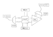
変調器デザイン
本発明は、相等しい光学的及び機能的特徴を有する薄いゲル層又は膜における、表面変調による光回折に基づく。基本的な変調器デザインおよび原理を図1に示す。変調器は、透明プリズムに取り付けられたゲルの薄層(又は膜)からなる。ゲル(膜)は、プリズムガラスとインデックスが整合しており、ゲル(膜)は、可視領域および赤外範囲の両方で低い光吸収(典型的システムについて、2%未満)を有する。典型的には、ゲル層は、厚さ15−30μmである。電極は、薄い空気ギャップ(厚さ5−10μm)によってゲル表面から分離した平滑基板層(図2)上に加工されている。空間は、当業者に公知の方法とは異なる様に配置できる。
Modulator design The present invention is based on light diffraction by surface modulation in a thin gel layer or film having equal optical and functional characteristics. The basic modulator design and principle is shown in FIG. The modulator consists of a thin layer (or film) of gel attached to a transparent prism. The gel (film) is index matched to the prism glass, and the gel (film) has low light absorption (less than 2% for typical systems) in both the visible and infrared ranges. Typically, the gel layer is 15-30 μm thick. The electrodes are processed on a smooth substrate layer (FIG. 2) separated from the gel surface by a thin air gap (thickness 5-10 μm). The space can be arranged differently from methods known to those skilled in the art.
バイアス電圧は、ゲルおよび空気ギャップを交差して適用される。結果として、電場のせいで正味の力がゲル表面に作用する。更に、各シグナル電極に個別にアドレスすることが可能である。局所シグナル電圧を適用することによって、力はゲル表面にかかり、表面変調が生じる。弾性表面応答は急速であり、応答時間は数十マイクロ秒である。しかし、種々のチャージおよび緩和プロセスもまた、ゲルにおいてより長い時間スケールで起こり、マイクロ秒から分の範囲で表面変調の遅いドリフトが生じる。本発明は、安定な作動のためのフィードバックの配置を提供する(下記)。 A bias voltage is applied across the gel and air gap. As a result, a net force acts on the gel surface due to the electric field. Furthermore, it is possible to address each signal electrode individually. By applying a local signal voltage, the force is applied to the gel surface, resulting in surface modulation. The elastic surface response is rapid and the response time is tens of microseconds. However, various charging and relaxation processes also occur at longer time scales in the gel, resulting in a slow drift of surface modulation in the microsecond to minute range. The present invention provides a feedback arrangement for stable operation (below).
図2に示す変調器の例の作用面積(電極)の典型的寸法は、3mm×6mmである。本発明の1実施態様のこの例では、電極は、最大解像度として125ラインペア/mmを有するインターレースのクシとして配置されている。解像度の限界は、表面変調の高密度のために必要な小さいゲル厚さおよび狭い空気ギャップのために必要な高精度のせいである。 A typical dimension of the active area (electrode) of the example modulator shown in FIG. 2 is 3 mm × 6 mm. In this example of one embodiment of the invention, the electrodes are arranged as interlaced combs having a maximum resolution of 125 line pairs / mm. The resolution limitation is due to the small gel thickness required for high density of surface modulation and the high accuracy required for narrow air gaps.
駆動電圧の周期的変動により、電圧と同周期のほぼ正弦の変調が生じる。電極にかけるバイアス電圧および駆動電圧の典型的値は100Vである。 Due to the periodic variation of the drive voltage, a nearly sinusoidal modulation with the same period as the voltage occurs. A typical value for the bias voltage and drive voltage applied to the electrodes is 100V.
変調した表面から光が反射される際、変調器は回折格子として働く。偏光効果および伝搬損失を減少させるために、円錐形回折構成が、高いライン密度のために使用される必要がある。光ビームの入射方向は、電極ラインと、表面変調の対応する溝(グルーブ)とに並行である。結果は、光がより高い回折次数に回折されるということである。 When light is reflected from the modulated surface, the modulator acts as a diffraction grating. In order to reduce polarization effects and propagation losses, conical diffractive configurations need to be used for high line densities. The incident direction of the light beam is parallel to the electrode line and the corresponding groove of the surface modulation. The result is that the light is diffracted to a higher diffraction order.
図3は、理論計算に基づく0次、1次および2次回折次数における強度を示す。強度は波長依存性であり、位相シフトは、1次までa/λに比例し、ここで、aは表面変調の振幅であり、λは光の波長である。Cバンドの波長の変動により、典型的には、1%の減衰の変動が生じるであろう。このことは、オフスイッチについての最良のゼロレベルが、Cバンド全体にわたって1%より悪いであろうことを意味する。表面変調の振幅を変化させることによって、0次の減衰は連続的に変化し得る。1550nmの光について、0次において完全な減衰に到達するために、300nmの表面変調の振幅が必要とされる。図3から分かり得るように、0次における完全減衰での1次における最大強度は、約30%である(最大のうちの1つについて)。 FIG. 3 shows intensities at the 0th, 1st and 2nd diffraction orders based on theoretical calculations. The intensity is wavelength dependent and the phase shift is proportional to a / λ up to first order, where a is the amplitude of the surface modulation and λ is the wavelength of the light. A variation in C-band wavelength will typically result in a 1% attenuation variation. This means that the best zero level for the off switch will be worse than 1% across the C band. By changing the amplitude of the surface modulation, the zero order attenuation can change continuously. For light at 1550 nm, a surface modulation amplitude of 300 nm is required to reach full attenuation in the 0th order. As can be seen from FIG. 3, the maximum intensity in the first order with complete attenuation in the 0th order is about 30% (for one of the maxima).
プリズムが高さ5mmで、幅が10mmである場合、1554nmの光が使用され、プリズムインデックス=1.45、以下の距離はプリズムファセット上で測定した。
0次と1次との間の距離は0.67mmである。
1次と2次次との間の距離は0.70mmである。
When the prism was 5 mm high and 10 mm wide, 1554 nm light was used, prism index = 1.45, distances below were measured on the prism facets.
The distance between the 0th order and the 1st order is 0.67 mm.
The distance between the primary and secondary is 0.70 mm.
これらの距離は、光ファイバとプリズム表面との連結のための位置を規定し、この連結は、当業者に公知のように行われる。 These distances define the position for the connection between the optical fiber and the prism surface, and this connection is made as known to those skilled in the art.
VOAの異なる配置
ゲルが配置された変調器は、プログラム可能な回折格子である。可変の振幅を有する正弦ゲルレリーフを有する格子が配置され得る。電極によって生じた電場は、ゲルの振幅を制御し、電極間の空間は、格子の周期を与える。変調器は、反射格子であり、入射角45°を有する(図4参照)。
Different arrangements of VOAs The modulator in which the gel is arranged is a programmable diffraction grating. A grating having a sinusoidal gel relief with variable amplitude may be placed. The electric field generated by the electrodes controls the amplitude of the gel and the space between the electrodes gives the period of the lattice. The modulator is a reflection grating and has an incident angle of 45 ° (see FIG. 4).
入射する光ビームの配向に依存して、回折は、円錐又は平面内回折であり得る。 Depending on the orientation of the incident light beam, the diffraction can be conical or in-plane diffraction.
構成1:円錐回折
プリズム頭頂部が電極ラインに垂直である場合、円錐回折が生じる。図5は、ゲルレリーフ振幅の関数として、異なる回折次数の強度を示す。格子の周期は8μmであり、これは、125ライン/mmに対応する。
Configuration 1: Conical diffraction occurs when the top of the conical diffraction prism is perpendicular to the electrode line. FIG. 5 shows the intensity of different diffraction orders as a function of gel relief amplitude. The period of the grating is 8 μm, which corresponds to 125 lines / mm.
円錐回折の利点:
−全ての光が格子によって反射され、光はゲルを通って伝搬されないであろう。
−この構成は、入射光の偏光にあまり依存しない。
−0次は、ゼロに非常に近くなるよう減少され得る。
Advantages of conical diffraction:
-All light will be reflected by the grating and no light will propagate through the gel.
-This configuration is less dependent on the polarization of the incident light.
The −0th order can be reduced to be very close to zero.
構成2:斜めの平面内回折
プリズム頭頂部が電極ラインに並行である場合、斜めの平面内回折が生じる。図6は、ゲルレリーフ振幅の関数として、異なる回折次数の強度を示す。格子の周期は8ミクロンであり、これは、125ライン/mmに対応する。
Configuration 2: When the top of the oblique in-plane diffraction prism is parallel to the electrode line, oblique in-plane diffraction occurs. FIG. 6 shows the intensity of different diffraction orders as a function of gel relief amplitude. The period of the grating is 8 microns, which corresponds to 125 lines / mm.
平面内回折の利点:
−回折次数の配向は、直線上である。これにより、平面内回折の変調器をデザインし、組み立てるのが容易になる。
−正及び負の回折次数は非対称である。非対称挙動により、幾つかの次数においてより高い強度が生じ、これは、スイッチデバイスにとってより効率的である。
Advantages of in-plane diffraction:
The orientation of the diffraction orders is linear. This makes it easier to design and assemble an in-plane diffraction modulator.
The positive and negative diffraction orders are asymmetric. Asymmetric behavior results in higher strength in some orders, which is more efficient for the switch device.
本発明の別の実施態様では、ゲルレリーフは、正弦形状から斜めの三角形状へ変化し、新しい回折特性が生じる。 In another embodiment of the invention, the gel relief changes from a sinusoidal shape to an oblique triangular shape, resulting in a new diffractive characteristic.
斜めの三角形状を有する格子は、ブレーズド(blazed)格子と言われる。ブレーズド格子では、ほとんど全ての光が、0次と特定の回折次数との間に分布されるであろう。これらの特徴によって、変調器は、スイッチとして働き得る。図7は、本発明のこのような実施態様の1例における各回折次数の強度をゲルレリーフ厚さの関数として示す。 A grid having an oblique triangular shape is called a blazed grid. In a blazed grating, almost all light will be distributed between the 0th order and a specific diffraction order. With these features, the modulator can act as a switch. FIG. 7 shows the intensity of each diffraction order as a function of gel relief thickness in one example of such an embodiment of the present invention.
電気通信区域におけるチューナブル表面回折格子の幾つかの適用について、できるだけ多くの回折光をインプット光ファイバに方向付けることが望ましい。しかし、実際には、回折次数において、アウトプット光パワーの対称分布が存在する。例えば、±1回折次数における光の最大強度は、+1次で33.9%に、−1次で33.9%に等しい(ゲル層表面での単色光および調波レリーフに関して)。回折次数における光の非対称分布を得るために、非対称レリーフを使用できる。このようなレリーフの可能な形状の1つは、ソーツース(鋸歯)プロフィールである。本発明は、ソーツースプロフィールを形成するための簡単な方法及びデバイスを提供する。 For some applications of tunable surface diffraction gratings in the telecommunications area, it is desirable to direct as much diffracted light as possible to the input optical fiber. However, in practice, there is a symmetric distribution of output optical power in the diffraction order. For example, the maximum intensity of light at ± 1 diffraction orders is equal to 33.9% for the + 1st order and 33.9% for the −1st order (for monochromatic light and harmonic relief on the gel layer surface). An asymmetric relief can be used to obtain an asymmetric distribution of light in the diffraction orders. One possible shape of such a relief is a sawtooth profile. The present invention provides a simple method and device for forming a sawtooth profile.
数学的アプローチ
最も原始的なソーツースプロフィールは、式(1)−(3)および図18から生じるので、2つの調波の合計として得られ得る。
Mathematical Approach The most primitive sawtooth profile arises from equations (1)-(3) and FIG. 18, so it can be obtained as the sum of two harmonics.

第2項F2(x)の振幅が20未満又は30を超える場合、図18と比較して、あまり良くないソーツース形状が生じるであろう。同じことが、第2項の位相シフトについて有効である:値π/2は、最も良く見えるソーツースプロフィールを与える。 If the amplitude of the second term F 2 (x) is less than 20 or more than 30, a sawtooth shape that is not very good will occur as compared to FIG. The same is valid for the second term phase shift: the value π / 2 gives the best looking sawtooth profile.
実際的履行
電極平面における電位分布のソーツースプロフィール(図18)は、図18においてプロットの下方に示す電極構造によって得られ得る。太いダッシュ線は、線状電極を表し、各ストローク上の値は、この電極に適用される電圧である。上方の線は項F1(x)に対応し、中央の線はF2(x)を表し、下部の線は合計FΣ(x)である。
A sawtooth profile of the potential distribution in a practical implementation electrode plane (FIG. 18) can be obtained by the electrode structure shown below the plot in FIG. A thick dash line represents a linear electrode, and the value on each stroke is the voltage applied to this electrode. The upper line corresponds to the term F 1 (x), the middle line represents F 2 (x), and the lower line is the total F Σ (x).
図18に示す電極平面における電位分布のソーツースプロフィールは、同一の形状のレリーフを形成しないであろうことを考慮すべきである。電位分布の空間調波の振幅は、電極平面からゲル層表面まで減少する。そして、該減少の速度は、調波項F2(x)に関して約2倍高い。なぜなら、それは、2倍大きい空間周波数(2倍小さい空間周期)を有するからである。調和的に分布したポンダー(ponder)原動力によって引き起こされる調波レリーフの振幅は、該力の一定の振幅に関して、空間周波数の増加と共に(又は、即ち、空間周期の減少と共に)減少する。 It should be considered that the sawtooth profile of the potential distribution at the electrode plane shown in FIG. 18 will not form a relief of the same shape. The amplitude of the spatial harmonic of the potential distribution decreases from the electrode plane to the gel layer surface. The rate of decrease is about twice as high with respect to the harmonic term F 2 (x). This is because it has a spatial frequency that is twice as large (a spatial period that is twice as small). The harmonic relief amplitude caused by the harmonically distributed ponder motive force decreases with increasing spatial frequency (ie, with decreasing spatial period) for a constant amplitude of the force.
このため、レリーフの第1空間調波の振幅A1(x)(電位の第1空間調波F1(x)によって引き起こされる)は、第2空間調波の振幅A2(x)(F2(x)によって引き起こされる)と比較して、100/25=4倍ではなく、例えば、6−8倍大きいであろう。そして、合計A1(x)+A2(x)は、合計F1(x)+F2(x)と比較して、あまり良くないソーツース形状を有するであろう。 Thus, the first spatial harmonic amplitude A 1 (x) of the relief (caused by the first spatial harmonic F 1 (x) of the potential) is the second spatial harmonic amplitude A 2 (x) (F 2 (x)) is not 100/25 = 4 times, for example 6-8 times larger. And the sum A 1 (x) + A 2 (x) will have a not so good sawtooth shape compared to the sum F 1 (x) + F 2 (x).
F2(x)の振幅の減少のより高い速度を補償するために、F2(x)に関してより大きい振幅を使用すべきである。それは、電極平面における電位分布のあまり良くないソーツース形状に対応するのではなく、レリーフの「正常な」(図18)ソーツース形状に対応するであろう。
To compensate for the higher rate of decrease in the amplitude of the
駆動モード
本発明の実施態様の開示例を駆動する際に生じる問題は、メモリー効果である。ゲルは、長期間そこに留まるならば、その形状に固定される。メモリー効果を除くために、異なるアプローチが使用できる。
・交互モード
電極は、1つおきの電極が電圧を有しかつ1つおきの電極が接地されているように、構成される。正弦格子周期は、1つの接地電極と電圧を有する1つの電極とによって作り出される。構成を周期的様式で逆にすることによって、メモリー効果を除くことが可能である。しかし、スイッチング時間の間、変調器を通して送られた光は制御できず、この方法による配置は、当業者に公知のように、電気通信適用において所望でない光を阻害する経路にオン/オフ光学シャッターデバイスを提供しなければならない。
・ローリング交互モード
ローリング交互モードは、1度に数ヶ所で2つの異なる駆動電圧の間で切り換えを行うだけであろう。情報は、変調器を通して連続的に送られ得る。位相シフトに関する問題は、経路における次なるデバイスにおいて補償され得る。
・フィードバックを有する静的モード
静的駆動モードでは、メモリー効果は生じるであろう。しかし、フィードバック制御システムによって、駆動シグナルは、メモリー効果に関して補償され得る。
Drive Mode A problem that arises when driving the disclosed example embodiments of the present invention is the memory effect. If the gel stays there for a long time, it will be fixed in its shape. Different approaches can be used to eliminate the memory effect.
Alternate mode electrodes are configured such that every other electrode has a voltage and every other electrode is grounded. A sinusoidal period is created by one ground electrode and one electrode having a voltage. It is possible to eliminate the memory effect by reversing the configuration in a periodic manner. However, during the switching time, the light sent through the modulator is not controllable and the arrangement according to this method is an on / off optical shutter in a path that obstructs unwanted light in telecommunications applications, as is known to those skilled in the art. Must provide a device.
Rolling alternate mode Rolling alternate mode will only switch between two different drive voltages at several locations at a time. Information can be sent continuously through the modulator. Problems with phase shift can be compensated for in the next device in the path.
Static mode with feedback In static drive mode, memory effects will occur. However, with the feedback control system, the drive signal can be compensated for memory effects.
ゲル変調器が励起電圧に供されると、ゲル表面上に波動パターンが設定され、これを用いて光学シグナルを偏光させるかまたは減衰させる。励起電圧が除去されると、ゲルは、即座には初期状態に戻らないであろう。 When the gel modulator is subjected to an excitation voltage, a wave pattern is set on the gel surface that is used to polarize or attenuate the optical signal. When the excitation voltage is removed, the gel will not return to its initial state immediately.
メモリー効果の結果は、ゲル変調器のVOA適用において、達成された減衰と適用した励起電圧との間に予測できる関係は存在しないであろうということである。 The result of the memory effect is that in a gel modulator VOA application, there will be no predictable relationship between the achieved attenuation and the applied excitation voltage.
従って、VOAの測定された減衰レベルは、変調器の励起電圧を制御するために、フィードバックシグナルとして使用される。フィードバックシステムを図13に示す。 Thus, the measured attenuation level of the VOA is used as a feedback signal to control the modulator excitation voltage. A feedback system is shown in FIG.
マスター制御ユニットは、減衰標的値をフィードバック制御ユニットに供給する。光学的インプットとアウトプットとが測定され、フィードバックループ制御ユニットは、変調器の減衰を測定する。この減衰値は標的値と比較され、訂正シグナルを与える。駆動電圧は、この訂正シグナルに基づいて調整される。典型的作動シーケンスを図14に示す。 The master control unit supplies the attenuation target value to the feedback control unit. The optical input and output are measured and the feedback loop control unit measures the modulator attenuation. This attenuation value is compared with the target value to give a correction signal. The drive voltage is adjusted based on this correction signal. A typical operating sequence is shown in FIG.
左手軸は、励起電極間の電圧差E=V1−V2を示す。右手軸はゲル減衰レベルAを示す。最初は、減衰はA1であり、定常状態励起電圧はE1である。t1で、マスター制御ユニットは、新しい標的レベルA2を受け取る。フィードバック制御ユニットは、励起電圧をE2に調整して新しい標的値を達成する。ゲルにおけるメモリー効果のせいで、励起電圧は、経時で定常状態レベルE3に落下するであろう。t2で、マスター制御ユニットは、標的値をスイッチしてA1に戻す。メモリー効果のせいで、フィードバックは、励起電圧をE4に減少させる。E4は負であり得、これは、V2電極がV1電極に対して正であることを示す。ある時間後、励起電圧は、定常状態値E5に近づくであろう。 The left hand axis shows the voltage difference E = V1-V2 between the excitation electrodes. The right hand axis shows the gel attenuation level A. Initially, the attenuation is A 1 and the steady state excitation voltage is E 1 . In t 1, the master control unit receives a new target level A 2. Feedback control unit adjusts the excitation voltage to E 2 to achieve the new target value. Because of the memory effect in the gel, the excitation voltage will fall to the steady-state levels E 3 over time. In t 2, the master control unit returns to A 1 to switch the target value. Because of the memory effect, the feedback reduces the excitation voltage E 4. E 4 can be a negative, this indicates that V2 electrode is positive with respect to V1 electrode. After some time, the excitation voltage will approach a steady state value E 5.
本発明は、幾つかの電気的チューナブル電気通信製品を生み出す潜在能力を有する進歩した材料プラットフォームとして、ゲル技術を提供する。電気通信適用からの要求に従うために、円錐回折(低い挿入損失、低い偏光依存性損失)及びフィードバックを有する静的駆動モード(高精度、データ損失無し)は、好適な作動モードである。 The present invention provides gel technology as an advanced material platform with the potential to create several electrically tunable telecommunications products. In order to comply with the requirements from telecommunications applications, a static drive mode (high accuracy, no data loss) with conical diffraction (low insertion loss, low polarization dependent loss) and feedback is a preferred mode of operation.
3つのコア機能は、本発明のこれらの方法:光変調、スペクトルフィルタリング、光学的スイッチングによって実施され得る。以下において、実施態様の例は、これらの機能を示す。 Three core functions can be implemented by these methods of the present invention: light modulation, spectral filtering, optical switching. In the following, example embodiments illustrate these functions.
実施態様のVOA例の2つの基本的型が示される。2つの適用を以下に記載する。 Two basic types of example VOA examples are shown. Two applications are described below.
125 l/mm基板に基づくVOA
以下の機能が、本発明の実施態様のこの例において実施された:
−可変減衰
−可変カプラー/タッパー(スイッチ)
−スペクトル選択性/フィルター
−モニタリング(フィードバック)
VOA based on 125 l / mm substrate
The following functions were implemented in this example of an embodiment of the invention:
-Variable damping-Variable coupler / tapper (switch)
-Spectral selectivity / filter-Monitoring (feedback)
実施態様の例は、オンチップモニタリング機能を有する2個の減衰器のアレイを有する。それは、2個の入射ファイバと4個の出射ファイバとを含む(図8参照)。+1次および−1次は、各入射チャネルにおいてパワーをモニターするために、エネルギーの限定部分を偏光させるためのテーパとして使用できる。スペクトル選択性はまた、コリメーティング光学の角度選択性を用いることによって、実行され得る。 An example embodiment has an array of two attenuators with on-chip monitoring capabilities. It includes two incoming fibers and four outgoing fibers (see FIG. 8). The + 1st order and -1st order can be used as a taper to polarize a limited portion of energy to monitor power in each incident channel. Spectral selectivity can also be performed by using the angular selectivity of collimating optics.
+1次および−1次からのフィードバックは、減衰範囲を増加させかつ精度を最適化するために使用される。 Feedback from the + 1st order and -1st order is used to increase the attenuation range and optimize accuracy.
33 l/mm基板に基づく実施態様の例
33 l/mm基板は、製造するのがより簡単でより安価であり、従って、考慮されるべきでもある。このような場合、回折ビームの非常に小さい角度の分離により、4個のファイバカップルのアウトプットの実際的製造は非常に困難になる。従って、「33 l/mm」変調器を用いる本発明の実施態様の例は、2個のインプットチャネルと2個のアウトプットチャネルとに基づくものであり、より高い回折次数を無視する。デバイスは、以下を有する:
・2個のチャネル用のゲルレリーフを制御する可能性を有する変調器。
・フィードバックループによって両方のチャネルの減衰レベルを制御するためのプログラム可能な制御エレクトロニクスボード。
Example Embodiment Based on 33 l / mm Substrate A 33 l / mm substrate is easier and cheaper to manufacture and therefore should also be considered. In such a case, the very small angular separation of the diffracted beam makes practical production of the output of four fiber couples very difficult. Thus, an example embodiment of the invention using a “33 l / mm” modulator is based on two input channels and two output channels, ignoring higher diffraction orders. The device has the following:
A modulator with the potential to control the gel relief for the two channels.
A programmable control electronics board for controlling the attenuation level of both channels by means of a feedback loop.
該実施態様の機能的スケッチを図9に示し、基板のレイアウトを図12に示す。 A functional sketch of the embodiment is shown in FIG. 9 and a substrate layout is shown in FIG.
チャネル当たり2個の光検出器は、変調器のインプットおよびアウトプットでの光学的パワーレベルに関する情報を提供するであろう。制御エレクトロニクスは、公称値に従って両方のチャネルでシグナルを正確に減衰させるために、この情報を用いて、ゲルに適用される電圧レベルを最適化する。 Two photodetectors per channel will provide information on the optical power levels at the input and output of the modulator. The control electronics uses this information to optimize the voltage level applied to the gel in order to accurately attenuate the signal in both channels according to the nominal value.
2つの主要な実施態様が可能である:
1.可変光減衰器
2つの主要な機能が必要である:
−使用者は、各チャネルに関して光学パワーのアウトプット値を規定し、インプット手段は、この値を制御エレクトロニクスに移し、該制御エレクトロニクスは、要求される光学パワーレベルが得られるまで、電圧レベルを最適化してシグナルを減衰させる。
例:Pin(チャネル1)=12mW、Pin(チャネル2)=10mW。
使用者設定:Pout(チャネル1)=6mW、Pout(チャネル2)=0.1mW。
Two main embodiments are possible:
1. Variable optical attenuator Two main functions are required:
-The user defines the optical power output value for each channel, the input means transfers this value to the control electronics, which optimizes the voltage level until the required optical power level is obtained. To attenuate the signal.
Example : P in (channel 1) = 12 mW, P in (channel 2) = 10 mW.
User setting: P out (channel 1) = 6 mW, P out (channel 2) = 0.1 mW.
変調器および制御エレクトロニクスは、使用者設定(即ち、第1チャネルで6mW、第2チャネルで0.1mW)に達するまで、両方のシグナルを減衰させる。2個のアウトプット光ダイオードからの値は、フィードバックループにおける最適化に使用される。
−使用者は、各チャネルに関して減衰のアウトプット値を規定する。制御エレクトロニクスは、要求される光学パワーレベルが得られるまで、電圧レベルを最適化してシグナルを減衰させる。
例:Pin(チャネル1)=12mW、Pin(チャネル2)=10mW。
使用者設定:減衰(チャネル1)=3dB、減衰(チャネル1)=20dB。
The modulator and control electronics attenuate both signals until a user setting is reached (ie 6 mW on the first channel and 0.1 mW on the second channel). The values from the two output photodiodes are used for optimization in the feedback loop.
-The user specifies the attenuation output value for each channel. The control electronics optimize the voltage level and attenuate the signal until the required optical power level is obtained.
Example : P in (channel 1) = 12 mW, P in (channel 2) = 10 mW.
User setting: attenuation (channel 1) = 3 dB, attenuation (channel 1) = 20 dB.
変調器および制御エレクトロニクスは、使用者設定(即ち、第1チャネルで6mW、第2チャネルで0.1mW)に達するまで、両方のシグナルを減衰させる。各チャネルにおいてインプットおよびアウトプット光ダイオードによって与えられる値の比は、フィードバックループにおける最適化に使用される。 The modulator and control electronics attenuate both signals until a user setting is reached (ie 6 mW on the first channel and 0.1 mW on the second channel). The ratio of the values given by the input and output photodiodes in each channel is used for optimization in the feedback loop.
本発明の実施態様のこの例は、動的チャネル等化を提供する。 This example of an embodiment of the present invention provides dynamic channel equalization.
経時で異なる強度を有する2つのチャネルは、デバイスに送られる。デバイスは、両方のチャネルが等化されるまで、最高の光学パワーを有するチャネルを動的に同定し減衰させる。等化は、1ミリ秒以内に行われる。 Two channels with different intensities over time are sent to the device. The device dynamically identifies and attenuates the channel with the highest optical power until both channels are equalized. Equalization takes place within 1 millisecond.
最後に、別の実施態様では、より高い減衰範囲を得るために、2つのチャネルを直列に接続することは有用であり得る。 Finally, in another embodiment, it may be useful to connect two channels in series to obtain a higher attenuation range.
偏光依存性損失
偏光依存性損失(PLD)の測定値は、実施態様の記載した例のいくつかについては僅かに高い。結果として、幾つかの二重又は多重パス構成が、PDLを相殺するために使用され得る。
Polarization Dependent Loss Polarization dependent loss (PLD) measurements are slightly higher for some of the described examples of embodiments. As a result, several dual or multipath configurations can be used to cancel PDL.
変調器のために多重パス構成を使用する2つの概念的方法がある。第1の方法は、第1の回折後、0次をピックアップし、次いで、この次数をもう1度回折させることである。アウトプットは、0次強度の平方であろう。これにより、非常に高い減衰を得る機会が得られる。0次のみをピックアップすることができるために、レンズ又はコリメータを使用してフラウンホーファー近似を得なければならない。図11は、二重パス構成を示す。 There are two conceptual ways to use a multipath configuration for the modulator. The first method is to pick up the 0th order after the first diffraction and then diffract this order one more time. The output will be the square of the 0th order intensity. This provides an opportunity to obtain very high attenuation. In order to be able to pick up only the zeroth order, a Fraunhofer approximation must be obtained using a lens or collimator. FIG. 11 shows a dual path configuration.
多重パス構成を行う他の方法は、回折ビームを鏡反射させ、それを再び回折させることである。この場合に、2つの回折間の距離は非常に近く、フレネル近似が用いられる。この種の配置によって、全位相シフトは、光ビームが回折パターンに当っている際に生じる全ての位相シフトの合計になるであろう。ビームが回折パターンにn回当っているならば、ゲルの振幅はn倍低くなければならず、およそ、電場はn倍小さくなければならない。 Another way to do a multi-pass configuration is to mirror the diffracted beam and diffract it again. In this case, the distance between the two diffractions is very close and the Fresnel approximation is used. With this type of arrangement, the total phase shift will be the sum of all phase shifts that occur when the light beam strikes the diffraction pattern. If the beam hits the diffraction pattern n times, the gel amplitude must be n times lower and the electric field should be about n times smaller.
他の適用
1×2スイッチ
簡単な1×2スイッチは、0次にて、および1次位置のうちの1つにて、コリメータを固定することによって実現化され得る。格子をオンおよびオフにスイッチングすることによって、光は、1つの位置から他の位置にスイッチされるであろう。(振幅を調整することによって、これはまた、可変タップとして役立ち得る)。可能な実施態様のスケッチを図15に示す。
Other applications
1 × 2 Switch A simple 1 × 2 switch can be realized by fixing the collimator in the zero order and one of the primary positions. By switching the grating on and off, the light will be switched from one position to another. (By adjusting the amplitude, this can also serve as a variable tap). A sketch of a possible embodiment is shown in FIG.
しかし、正弦格子の異なる回折次数の強度分布に基づいて、円錐形のジオメトリを有する変調器は、約30%で1次のうちの1つの最大強度を有するであろう。これは、0次が最小である場合、そうではない。 However, based on the intensity distribution of the different diffraction orders of the sinusoidal grating, a modulator having a conical geometry will have a maximum intensity of one of the first orders at about 30%. This is not the case when the 0th order is minimal.
(上記のように)ブレーズド格子を形成することは、これらの特徴を、選択された1次において効率90%まで劇的に改善する可能性を与える(図15参照)。 Forming a blazed grating (as described above) gives the possibility to dramatically improve these features to 90% efficiency in the chosen first order (see FIG. 15).
動的ゲインイコライザー
チャネルイコライザー、即ち、ゲイン平滑化デバイスは、自由空間デマックス(demux)とVOAアレイとの組合せとして製造できる。チャネルイコライザーは、回折格子や薄膜フィルターなどのデマックス素子との組合せでVOA素子を有し、これは、光学シグナルを分散させ、それによって、個々の波長が空間で分離される。一体化したVOA素子を有するDGE素子を示す例を図16に示す。
A dynamic gain equalizer channel equalizer, or gain smoothing device, can be manufactured as a combination of a free space demux and a VOA array. A channel equalizer has a VOA element in combination with a demax element such as a diffraction grating or a thin film filter, which disperses the optical signal, thereby separating the individual wavelengths in space. An example showing a DGE element having an integrated VOA element is shown in FIG.
R−OADM−再構成可能な光加算−減算(Add-Drop)マルチプレクサ
ゲル変調器の性質は自由空間なので、多重光学機能のハイブリッド統合化(マックス/デマックス(mux/demux)、スイッチアレイ及びVOAアレイ)を行ってR−OADMを構築することが可能である。
R-OADM-Reconfigurable Optical Add-Drop Multiplexer Gel Modulators are free space, so hybrid integration of multiple optical functions (mux / demux, switch arrays and VOA arrays ) To construct the R-OADM.
本発明によるR−OADMハイブリッドデバイスの実施態様の例を図17に示す。 An example embodiment of an R-OADM hybrid device according to the present invention is shown in FIG.
モニタリングデバイス
回折原理は、例えば、モニタリングアウトプットとして1次のうちの1つを使用することによって、適用をモニターするのに適しており、一方、変調器はまた、いくつかの他の光学機能を送達する。光学チャネルモニター(OCM)はまた、フィードバックシステムにおいてタップで較正した検出器を用いることによって実行し得る。
The monitoring device diffraction principle is suitable for monitoring the application, for example by using one of the first orders as the monitoring output, while the modulator also has several other optical functions. Deliver. An optical channel monitor (OCM) can also be implemented by using a tap calibrated detector in the feedback system.
Claims (14)
当該方法は、
透明プリズムに隣接して取り付けられたゲル層又は膜を提供するステップを有し、該プリズムは、該光通信システムへ/該光通信システムから、光を送るおよび/または光を受け取るものであり、
1セットの個別にアドレス可能な電極を基板に提供するステップを有し、該電極は、該プリズムとは反対側を向いた該ゲル又は膜の表面から、適切な間隔を置いて配置されており、
各電極に励起電圧を加えるための手段を提供するステップを有し、これによって、波動パターンを該ゲル又は膜層の表面上に提供して、該ゲル又は膜層の初期状態に重畳させ、
励起電圧を除去して該ゲル又は膜層が該初期状態に戻るように、電極への励起電圧を制御するステップを有すること、
を特徴とする前記方法。 A method for providing modulation of light in an optical communication system comprising:
The method is
Providing a gel layer or film attached adjacent to the transparent prism, the prism sending and / or receiving light to / from the optical communication system;
Providing a set of individually addressable electrodes to the substrate, the electrodes being appropriately spaced from the surface of the gel or membrane facing away from the prism ,
Providing a means for applying an excitation voltage to each electrode, whereby a wave pattern is provided on the surface of the gel or membrane layer and superimposed on the initial state of the gel or membrane layer;
Controlling the excitation voltage to the electrode so that the excitation voltage is removed and the gel or membrane layer returns to the initial state;
A method as described above.
ゲル又は膜層を有し、
光通信システムへ/光通信システムから、光を伝達するプリズムを有し、該ゲル又は膜層は、該プリズムの表面に隣接して取り付けられており、
複数の個別にアドレス可能な電極を有する基板を有し、該電極は、該プリズム表面とは反対側を向いた該ゲル又は膜層の表面からある距離を置いて位置しており、
該複数の電極の各々に制御された励起電圧を提供する駆動手段を有し、該駆動手段は波動パターンを該ゲル又は膜層の表面上に提供して、該ゲル又は膜層の初期状態に重畳させ、該駆動手段は、該励起電圧を除去した際に、該ゲル又は膜層を該初期状態に戻させる補償手段を有すること、
を特徴とする前記デバイス。 A device for modulating light in an optical communication system, the device comprising:
Having a gel or membrane layer,
A prism for transmitting light to / from the optical communication system, the gel or film layer being attached adjacent to the surface of the prism;
A substrate having a plurality of individually addressable electrodes, the electrodes being located at a distance from the surface of the gel or membrane layer facing away from the prism surface;
Driving means for providing a controlled excitation voltage to each of the plurality of electrodes, the driving means providing a wave pattern on the surface of the gel or film layer to bring the gel or film layer into an initial state; The driving means has a compensation means for returning the gel or film layer to the initial state when the excitation voltage is removed;
Said device.
Applications Claiming Priority (3)
| Application Number | Priority Date | Filing Date | Title |
|---|---|---|---|
| US40912602P | 2002-09-06 | 2002-09-06 | |
| NO20024265A NO318004B1 (en) | 2002-09-06 | 2002-09-06 | Method and apparatus for a variable optical attenuator |
| PCT/NO2003/000304 WO2004023197A1 (en) | 2002-09-06 | 2003-08-29 | Method and device for variable optical attenuator |
Publications (1)
| Publication Number | Publication Date |
|---|---|
| JP2005525604A true JP2005525604A (en) | 2005-08-25 |
Family
ID=31980710
Family Applications (1)
| Application Number | Title | Priority Date | Filing Date |
|---|---|---|---|
| JP2004533890A Pending JP2005525604A (en) | 2002-09-06 | 2003-08-29 | Method and device for variable optical attenuator |
Country Status (6)
| Country | Link |
|---|---|
| US (1) | US6897995B2 (en) |
| EP (1) | EP1535108A1 (en) |
| JP (1) | JP2005525604A (en) |
| CN (1) | CN100520485C (en) |
| AU (1) | AU2003263690A1 (en) |
| WO (1) | WO2004023197A1 (en) |
Families Citing this family (13)
| Publication number | Priority date | Publication date | Assignee | Title |
|---|---|---|---|---|
| NO20033940D0 (en) | 2003-09-05 | 2003-09-05 | Photonyx As | Method and apparatus for reducing polarization dependent effects in a controllable optical component |
| US7133184B2 (en) * | 2004-06-03 | 2006-11-07 | Samsung Electro-Mechanics Co., Ltd. | Variable grating diffractive light modulator |
| NO327026B1 (en) * | 2005-12-06 | 2009-04-06 | Ignis Display As | Method for Increasing the Surface Conductivity of a Polymer Used in a Adjustable Diffraction Grid (TDG) Modulator |
| NO326468B1 (en) * | 2005-12-06 | 2008-12-08 | Ignis Display As | Modulator with adjustable diffraction grating (TDG) with total internal reflection (TIR), method for producing an elastomer for use therein and use of the elastomer. |
| NO20055796D0 (en) * | 2005-12-07 | 2005-12-07 | Ignis Photonyx As | Line scan projection display system including a dual pixel radius light modulator |
| WO2007081220A1 (en) * | 2006-01-13 | 2007-07-19 | Ignis Display As | Dynamic pixel structure |
| US8150267B1 (en) | 2007-04-18 | 2012-04-03 | Hewlett-Packard Development Company, L.P. | Optical interconnect |
| US8659835B2 (en) | 2009-03-13 | 2014-02-25 | Optotune Ag | Lens systems and method |
| US8699141B2 (en) | 2009-03-13 | 2014-04-15 | Knowles Electronics, Llc | Lens assembly apparatus and method |
| EP2296019A1 (en) | 2009-09-14 | 2011-03-16 | poLight AS | Optical power switch (OPS) |
| EP2322957A1 (en) | 2009-11-12 | 2011-05-18 | poLight AS | A method, device and system for reducing speckle contrast |
| JP2012156285A (en) * | 2011-01-26 | 2012-08-16 | Fujitsu Ltd | Light amplifier |
| CN112933449B (en) * | 2021-01-13 | 2022-01-21 | 安徽大学 | Biological piezoelectric type intelligent mask and intelligent control method thereof |
Family Cites Families (18)
| Publication number | Priority date | Publication date | Assignee | Title |
|---|---|---|---|---|
| CH454296A (en) * | 1967-03-17 | 1968-04-15 | Foerderung Forschung Gmbh | Device for amplifying the intensity of an optically generated image |
| CH537129A (en) | 1971-10-27 | 1973-05-15 | Eidophor Ag | Projection device, in particular for television pictures |
| US4529620A (en) | 1984-01-30 | 1985-07-16 | New York Institute Of Technology | Method of making deformable light modulator structure |
| US4635082A (en) * | 1984-05-17 | 1987-01-06 | Xerox Corporation | Thermo-optic light modulation array |
| US4857978A (en) | 1987-08-11 | 1989-08-15 | North American Philips Corporation | Solid state light modulator incorporating metallized gel and method of metallization |
| US4900136A (en) | 1987-08-11 | 1990-02-13 | North American Philips Corporation | Method of metallizing silica-containing gel and solid state light modulator incorporating the metallized gel |
| US4879602A (en) | 1987-09-04 | 1989-11-07 | New York Institute Of Technology | Electrode patterns for solid state light modulator |
| US5221747A (en) | 1989-01-19 | 1993-06-22 | Reilly Industries, Inc. | Improved process and catalyst for the preparation of 2,2' bipyridyls |
| US5116674A (en) | 1989-01-27 | 1992-05-26 | Ciba-Geigy Corporation | Composite structure |
| GB2265024B (en) * | 1992-03-14 | 1996-01-24 | British Aerospace | A spatial light modulator assembly |
| US5867301A (en) | 1996-04-22 | 1999-02-02 | Engle; Craig D. | Phase modulating device |
| EP1023621A4 (en) | 1997-08-13 | 2001-08-08 | Foster Miller Inc | Switchable optical components |
| DE69828034T2 (en) * | 1998-01-20 | 2005-04-21 | Seiko Epson Corp | OPTICAL SWITCHING DEVICE, IMAGE DISPLAY AND PROJECTION DEVICE |
| US6369936B1 (en) * | 1999-03-12 | 2002-04-09 | Kodak Polychrome Graphics Llc | Pixel intensity control in electro-optic modulators |
| GB9930555D0 (en) | 1999-12-23 | 2000-02-16 | Opti Switch As | Optical systems |
| US6456419B1 (en) * | 2000-09-29 | 2002-09-24 | Innovative Technology Licensing, Llc | Frequency modulated liquid crystal beamsteering device |
| US6587288B2 (en) * | 2001-03-12 | 2003-07-01 | Optical Coating Laboratory, Inc. | Optical attenuation filter |
| JP2002365603A (en) * | 2001-06-12 | 2002-12-18 | Minolta Co Ltd | Optical shutter device |
-
2003
- 2003-08-29 JP JP2004533890A patent/JP2005525604A/en active Pending
- 2003-08-29 EP EP03794360A patent/EP1535108A1/en not_active Withdrawn
- 2003-08-29 AU AU2003263690A patent/AU2003263690A1/en not_active Abandoned
- 2003-08-29 WO PCT/NO2003/000304 patent/WO2004023197A1/en active Application Filing
- 2003-09-05 CN CNB031255574A patent/CN100520485C/en not_active Expired - Fee Related
- 2003-09-05 US US10/656,009 patent/US6897995B2/en not_active Expired - Lifetime
Also Published As
| Publication number | Publication date |
|---|---|
| CN100520485C (en) | 2009-07-29 |
| WO2004023197A1 (en) | 2004-03-18 |
| US6897995B2 (en) | 2005-05-24 |
| AU2003263690A1 (en) | 2004-03-29 |
| CN1495454A (en) | 2004-05-12 |
| EP1535108A1 (en) | 2005-06-01 |
| US20040130773A1 (en) | 2004-07-08 |
Similar Documents
| Publication | Publication Date | Title |
|---|---|---|
| US11243450B2 (en) | Saw modulator having optical power component for extended angular redirection of light | |
| US7085492B2 (en) | Wavelength division multiplexed device | |
| US7019883B2 (en) | Dynamic optical filter having a spatial light modulator | |
| US7352927B2 (en) | Optical add-drop multiplexer architecture with reduced effect of mirror edge diffraction | |
| EP1497682B1 (en) | Tunable optical filter | |
| US7346234B2 (en) | Reduction of MEMS mirror edge diffraction in a wavelength selective switch using servo-based multi-axes rotation | |
| CN104204916B (en) | optical device and method | |
| EP1292857B1 (en) | Dynamically variable diffractive optical devices | |
| JP5692865B2 (en) | Wavelength cross-connect equipment | |
| JP5730526B2 (en) | Light switch | |
| EP1400047A2 (en) | Wavelength division multiplexed device | |
| JP2005525604A (en) | Method and device for variable optical attenuator | |
| KR20030064850A (en) | MEMS Reconfigurable Optical Grating | |
| US20030206681A1 (en) | Integrating element for optical fiber communication systems based on photonic multi-bandgap quasi-crystals having optimized transfer functions | |
| JP2002267998A (en) | Wavelength dispersion compensation module, optical receiving circuit, and optical communication system | |
| WO2001011419A9 (en) | Dynamic spectral shaping in optical fibre communication | |
| US20030206694A1 (en) | Photonic multi-bandgap lightwave device and methods for manufacturing thereof | |
| JPH03211529A (en) | Optical multiplexer and demultiplexer integrated at high density | |
| WO2001086848A1 (en) | Optical wavelength division multiplexer and de-multiplexer | |
| CA2490768A1 (en) | Method and apparatus for detecting multiple optical wave lengths | |
| KR100637917B1 (en) | Method and device for variable optical attenuator | |
| JP2005099800A (en) | Spatial phase filter for light beam, filter system and filter calculation method | |
| KR100839335B1 (en) | Application apparatus for reflective micro optic interferometric filter | |
| Yu | Optical signal processing with MEMS technology: Applications in optical communication systems | |
| TW202032931A (en) | Wavelength selective enable bidirectional access system |
Legal Events
| Date | Code | Title | Description |
|---|---|---|---|
| A977 | Report on retrieval |
Free format text: JAPANESE INTERMEDIATE CODE: A971007 Effective date: 20070615 |
|
| A131 | Notification of reasons for refusal |
Free format text: JAPANESE INTERMEDIATE CODE: A131 Effective date: 20071002 |
|
| A601 | Written request for extension of time |
Free format text: JAPANESE INTERMEDIATE CODE: A601 Effective date: 20071212 |
|
| A602 | Written permission of extension of time |
Free format text: JAPANESE INTERMEDIATE CODE: A602 Effective date: 20071219 |
|
| A02 | Decision of refusal |
Free format text: JAPANESE INTERMEDIATE CODE: A02 Effective date: 20080507 |