JP2005513585A - Selective metal removal method for metallized retroreflective and holographic films and radio frequency device produced by the method - Google Patents
Selective metal removal method for metallized retroreflective and holographic films and radio frequency device produced by the method Download PDFInfo
- Publication number
- JP2005513585A JP2005513585A JP2002586510A JP2002586510A JP2005513585A JP 2005513585 A JP2005513585 A JP 2005513585A JP 2002586510 A JP2002586510 A JP 2002586510A JP 2002586510 A JP2002586510 A JP 2002586510A JP 2005513585 A JP2005513585 A JP 2005513585A
- Authority
- JP
- Japan
- Prior art keywords
- antenna
- metallized
- layer
- base layer
- metal
- Prior art date
- Legal status (The legal status is an assumption and is not a legal conclusion. Google has not performed a legal analysis and makes no representation as to the accuracy of the status listed.)
- Pending
Links
Images


Classifications
-
- G—PHYSICS
- G06—COMPUTING; CALCULATING OR COUNTING
- G06K—GRAPHICAL DATA READING; PRESENTATION OF DATA; RECORD CARRIERS; HANDLING RECORD CARRIERS
- G06K19/00—Record carriers for use with machines and with at least a part designed to carry digital markings
- G06K19/06—Record carriers for use with machines and with at least a part designed to carry digital markings characterised by the kind of the digital marking, e.g. shape, nature, code
- G06K19/067—Record carriers with conductive marks, printed circuits or semiconductor circuit elements, e.g. credit or identity cards also with resonating or responding marks without active components
- G06K19/07—Record carriers with conductive marks, printed circuits or semiconductor circuit elements, e.g. credit or identity cards also with resonating or responding marks without active components with integrated circuit chips
- G06K19/0723—Record carriers with conductive marks, printed circuits or semiconductor circuit elements, e.g. credit or identity cards also with resonating or responding marks without active components with integrated circuit chips the record carrier comprising an arrangement for non-contact communication, e.g. wireless communication circuits on transponder cards, non-contact smart cards or RFIDs
-
- G—PHYSICS
- G06—COMPUTING; CALCULATING OR COUNTING
- G06K—GRAPHICAL DATA READING; PRESENTATION OF DATA; RECORD CARRIERS; HANDLING RECORD CARRIERS
- G06K19/00—Record carriers for use with machines and with at least a part designed to carry digital markings
- G06K19/06—Record carriers for use with machines and with at least a part designed to carry digital markings characterised by the kind of the digital marking, e.g. shape, nature, code
- G06K19/067—Record carriers with conductive marks, printed circuits or semiconductor circuit elements, e.g. credit or identity cards also with resonating or responding marks without active components
- G06K19/07—Record carriers with conductive marks, printed circuits or semiconductor circuit elements, e.g. credit or identity cards also with resonating or responding marks without active components with integrated circuit chips
- G06K19/077—Constructional details, e.g. mounting of circuits in the carrier
- G06K19/07718—Constructional details, e.g. mounting of circuits in the carrier the record carrier being manufactured in a continuous process, e.g. using endless rolls
-
- G—PHYSICS
- G06—COMPUTING; CALCULATING OR COUNTING
- G06K—GRAPHICAL DATA READING; PRESENTATION OF DATA; RECORD CARRIERS; HANDLING RECORD CARRIERS
- G06K19/00—Record carriers for use with machines and with at least a part designed to carry digital markings
- G06K19/06—Record carriers for use with machines and with at least a part designed to carry digital markings characterised by the kind of the digital marking, e.g. shape, nature, code
- G06K19/067—Record carriers with conductive marks, printed circuits or semiconductor circuit elements, e.g. credit or identity cards also with resonating or responding marks without active components
- G06K19/07—Record carriers with conductive marks, printed circuits or semiconductor circuit elements, e.g. credit or identity cards also with resonating or responding marks without active components with integrated circuit chips
- G06K19/077—Constructional details, e.g. mounting of circuits in the carrier
- G06K19/07745—Mounting details of integrated circuit chips
-
- G—PHYSICS
- G06—COMPUTING; CALCULATING OR COUNTING
- G06K—GRAPHICAL DATA READING; PRESENTATION OF DATA; RECORD CARRIERS; HANDLING RECORD CARRIERS
- G06K19/00—Record carriers for use with machines and with at least a part designed to carry digital markings
- G06K19/06—Record carriers for use with machines and with at least a part designed to carry digital markings characterised by the kind of the digital marking, e.g. shape, nature, code
- G06K19/067—Record carriers with conductive marks, printed circuits or semiconductor circuit elements, e.g. credit or identity cards also with resonating or responding marks without active components
- G06K19/07—Record carriers with conductive marks, printed circuits or semiconductor circuit elements, e.g. credit or identity cards also with resonating or responding marks without active components with integrated circuit chips
- G06K19/077—Constructional details, e.g. mounting of circuits in the carrier
- G06K19/07749—Constructional details, e.g. mounting of circuits in the carrier the record carrier being capable of non-contact communication, e.g. constructional details of the antenna of a non-contact smart card
- G06K19/0775—Constructional details, e.g. mounting of circuits in the carrier the record carrier being capable of non-contact communication, e.g. constructional details of the antenna of a non-contact smart card arrangements for connecting the integrated circuit to the antenna
-
- G—PHYSICS
- G06—COMPUTING; CALCULATING OR COUNTING
- G06K—GRAPHICAL DATA READING; PRESENTATION OF DATA; RECORD CARRIERS; HANDLING RECORD CARRIERS
- G06K19/00—Record carriers for use with machines and with at least a part designed to carry digital markings
- G06K19/06—Record carriers for use with machines and with at least a part designed to carry digital markings characterised by the kind of the digital marking, e.g. shape, nature, code
- G06K19/067—Record carriers with conductive marks, printed circuits or semiconductor circuit elements, e.g. credit or identity cards also with resonating or responding marks without active components
- G06K19/07—Record carriers with conductive marks, printed circuits or semiconductor circuit elements, e.g. credit or identity cards also with resonating or responding marks without active components with integrated circuit chips
- G06K19/077—Constructional details, e.g. mounting of circuits in the carrier
- G06K19/07749—Constructional details, e.g. mounting of circuits in the carrier the record carrier being capable of non-contact communication, e.g. constructional details of the antenna of a non-contact smart card
- G06K19/07758—Constructional details, e.g. mounting of circuits in the carrier the record carrier being capable of non-contact communication, e.g. constructional details of the antenna of a non-contact smart card arrangements for adhering the record carrier to further objects or living beings, functioning as an identification tag
- G06K19/0776—Constructional details, e.g. mounting of circuits in the carrier the record carrier being capable of non-contact communication, e.g. constructional details of the antenna of a non-contact smart card arrangements for adhering the record carrier to further objects or living beings, functioning as an identification tag the adhering arrangement being a layer of adhesive, so that the record carrier can function as a sticker
-
- G—PHYSICS
- G06—COMPUTING; CALCULATING OR COUNTING
- G06K—GRAPHICAL DATA READING; PRESENTATION OF DATA; RECORD CARRIERS; HANDLING RECORD CARRIERS
- G06K19/00—Record carriers for use with machines and with at least a part designed to carry digital markings
- G06K19/06—Record carriers for use with machines and with at least a part designed to carry digital markings characterised by the kind of the digital marking, e.g. shape, nature, code
- G06K19/067—Record carriers with conductive marks, printed circuits or semiconductor circuit elements, e.g. credit or identity cards also with resonating or responding marks without active components
- G06K19/07—Record carriers with conductive marks, printed circuits or semiconductor circuit elements, e.g. credit or identity cards also with resonating or responding marks without active components with integrated circuit chips
- G06K19/077—Constructional details, e.g. mounting of circuits in the carrier
- G06K19/07749—Constructional details, e.g. mounting of circuits in the carrier the record carrier being capable of non-contact communication, e.g. constructional details of the antenna of a non-contact smart card
- G06K19/07771—Constructional details, e.g. mounting of circuits in the carrier the record carrier being capable of non-contact communication, e.g. constructional details of the antenna of a non-contact smart card the record carrier comprising means for minimising adverse effects on the data communication capability of the record carrier, e.g. minimising Eddy currents induced in a proximate metal or otherwise electromagnetically interfering object
-
- G—PHYSICS
- G06—COMPUTING; CALCULATING OR COUNTING
- G06K—GRAPHICAL DATA READING; PRESENTATION OF DATA; RECORD CARRIERS; HANDLING RECORD CARRIERS
- G06K19/00—Record carriers for use with machines and with at least a part designed to carry digital markings
- G06K19/06—Record carriers for use with machines and with at least a part designed to carry digital markings characterised by the kind of the digital marking, e.g. shape, nature, code
- G06K19/067—Record carriers with conductive marks, printed circuits or semiconductor circuit elements, e.g. credit or identity cards also with resonating or responding marks without active components
- G06K19/07—Record carriers with conductive marks, printed circuits or semiconductor circuit elements, e.g. credit or identity cards also with resonating or responding marks without active components with integrated circuit chips
- G06K19/077—Constructional details, e.g. mounting of circuits in the carrier
- G06K19/07749—Constructional details, e.g. mounting of circuits in the carrier the record carrier being capable of non-contact communication, e.g. constructional details of the antenna of a non-contact smart card
- G06K19/07773—Antenna details
- G06K19/07777—Antenna details the antenna being of the inductive type
- G06K19/07779—Antenna details the antenna being of the inductive type the inductive antenna being a coil
- G06K19/07783—Antenna details the antenna being of the inductive type the inductive antenna being a coil the coil being planar
-
- H—ELECTRICITY
- H05—ELECTRIC TECHNIQUES NOT OTHERWISE PROVIDED FOR
- H05K—PRINTED CIRCUITS; CASINGS OR CONSTRUCTIONAL DETAILS OF ELECTRIC APPARATUS; MANUFACTURE OF ASSEMBLAGES OF ELECTRICAL COMPONENTS
- H05K1/00—Printed circuits
- H05K1/02—Details
- H05K1/0266—Marks, test patterns or identification means
- H05K1/0269—Marks, test patterns or identification means for visual or optical inspection
-
- H—ELECTRICITY
- H05—ELECTRIC TECHNIQUES NOT OTHERWISE PROVIDED FOR
- H05K—PRINTED CIRCUITS; CASINGS OR CONSTRUCTIONAL DETAILS OF ELECTRIC APPARATUS; MANUFACTURE OF ASSEMBLAGES OF ELECTRICAL COMPONENTS
- H05K3/00—Apparatus or processes for manufacturing printed circuits
- H05K3/02—Apparatus or processes for manufacturing printed circuits in which the conductive material is applied to the surface of the insulating support and is thereafter removed from such areas of the surface which are not intended for current conducting or shielding
- H05K3/06—Apparatus or processes for manufacturing printed circuits in which the conductive material is applied to the surface of the insulating support and is thereafter removed from such areas of the surface which are not intended for current conducting or shielding the conductive material being removed chemically or electrolytically, e.g. by photo-etch process
- H05K3/067—Etchants
-
- G—PHYSICS
- G06—COMPUTING; CALCULATING OR COUNTING
- G06K—GRAPHICAL DATA READING; PRESENTATION OF DATA; RECORD CARRIERS; HANDLING RECORD CARRIERS
- G06K19/00—Record carriers for use with machines and with at least a part designed to carry digital markings
- G06K19/06—Record carriers for use with machines and with at least a part designed to carry digital markings characterised by the kind of the digital marking, e.g. shape, nature, code
- G06K2019/06215—Aspects not covered by other subgroups
- G06K2019/0629—Holographic, diffractive or retroreflective recording
-
- H—ELECTRICITY
- H01—ELECTRIC ELEMENTS
- H01L—SEMICONDUCTOR DEVICES NOT COVERED BY CLASS H10
- H01L2924/00—Indexing scheme for arrangements or methods for connecting or disconnecting semiconductor or solid-state bodies as covered by H01L24/00
- H01L2924/0001—Technical content checked by a classifier
- H01L2924/0002—Not covered by any one of groups H01L24/00, H01L24/00 and H01L2224/00
-
- H—ELECTRICITY
- H05—ELECTRIC TECHNIQUES NOT OTHERWISE PROVIDED FOR
- H05K—PRINTED CIRCUITS; CASINGS OR CONSTRUCTIONAL DETAILS OF ELECTRIC APPARATUS; MANUFACTURE OF ASSEMBLAGES OF ELECTRICAL COMPONENTS
- H05K1/00—Printed circuits
- H05K1/02—Details
- H05K1/0274—Optical details, e.g. printed circuits comprising integral optical means
-
- H—ELECTRICITY
- H05—ELECTRIC TECHNIQUES NOT OTHERWISE PROVIDED FOR
- H05K—PRINTED CIRCUITS; CASINGS OR CONSTRUCTIONAL DETAILS OF ELECTRIC APPARATUS; MANUFACTURE OF ASSEMBLAGES OF ELECTRICAL COMPONENTS
- H05K1/00—Printed circuits
- H05K1/02—Details
- H05K1/03—Use of materials for the substrate
- H05K1/0393—Flexible materials
-
- H—ELECTRICITY
- H05—ELECTRIC TECHNIQUES NOT OTHERWISE PROVIDED FOR
- H05K—PRINTED CIRCUITS; CASINGS OR CONSTRUCTIONAL DETAILS OF ELECTRIC APPARATUS; MANUFACTURE OF ASSEMBLAGES OF ELECTRICAL COMPONENTS
- H05K2201/00—Indexing scheme relating to printed circuits covered by H05K1/00
- H05K2201/01—Dielectrics
- H05K2201/0104—Properties and characteristics in general
- H05K2201/0133—Elastomeric or compliant polymer
-
- H—ELECTRICITY
- H05—ELECTRIC TECHNIQUES NOT OTHERWISE PROVIDED FOR
- H05K—PRINTED CIRCUITS; CASINGS OR CONSTRUCTIONAL DETAILS OF ELECTRIC APPARATUS; MANUFACTURE OF ASSEMBLAGES OF ELECTRICAL COMPONENTS
- H05K2201/00—Indexing scheme relating to printed circuits covered by H05K1/00
- H05K2201/09—Shape and layout
- H05K2201/09209—Shape and layout details of conductors
- H05K2201/09654—Shape and layout details of conductors covering at least two types of conductors provided for in H05K2201/09218 - H05K2201/095
- H05K2201/09781—Dummy conductors, i.e. not used for normal transport of current; Dummy electrodes of components
-
- H—ELECTRICITY
- H05—ELECTRIC TECHNIQUES NOT OTHERWISE PROVIDED FOR
- H05K—PRINTED CIRCUITS; CASINGS OR CONSTRUCTIONAL DETAILS OF ELECTRIC APPARATUS; MANUFACTURE OF ASSEMBLAGES OF ELECTRICAL COMPONENTS
- H05K2201/00—Indexing scheme relating to printed circuits covered by H05K1/00
- H05K2201/09—Shape and layout
- H05K2201/09818—Shape or layout details not covered by a single group of H05K2201/09009 - H05K2201/09809
- H05K2201/09936—Marks, inscriptions, etc. for information
-
- H—ELECTRICITY
- H05—ELECTRIC TECHNIQUES NOT OTHERWISE PROVIDED FOR
- H05K—PRINTED CIRCUITS; CASINGS OR CONSTRUCTIONAL DETAILS OF ELECTRIC APPARATUS; MANUFACTURE OF ASSEMBLAGES OF ELECTRICAL COMPONENTS
- H05K2201/00—Indexing scheme relating to printed circuits covered by H05K1/00
- H05K2201/20—Details of printed circuits not provided for in H05K2201/01 - H05K2201/10
- H05K2201/2054—Light-reflecting surface, e.g. conductors, substrates, coatings, dielectrics
-
- H—ELECTRICITY
- H05—ELECTRIC TECHNIQUES NOT OTHERWISE PROVIDED FOR
- H05K—PRINTED CIRCUITS; CASINGS OR CONSTRUCTIONAL DETAILS OF ELECTRIC APPARATUS; MANUFACTURE OF ASSEMBLAGES OF ELECTRICAL COMPONENTS
- H05K2203/00—Indexing scheme relating to apparatus or processes for manufacturing printed circuits covered by H05K3/00
- H05K2203/01—Tools for processing; Objects used during processing
- H05K2203/0104—Tools for processing; Objects used during processing for patterning or coating
- H05K2203/0143—Using a roller; Specific shape thereof; Providing locally adhesive portions thereon
-
- H—ELECTRICITY
- H05—ELECTRIC TECHNIQUES NOT OTHERWISE PROVIDED FOR
- H05K—PRINTED CIRCUITS; CASINGS OR CONSTRUCTIONAL DETAILS OF ELECTRIC APPARATUS; MANUFACTURE OF ASSEMBLAGES OF ELECTRICAL COMPONENTS
- H05K2203/00—Indexing scheme relating to apparatus or processes for manufacturing printed circuits covered by H05K3/00
- H05K2203/15—Position of the PCB during processing
- H05K2203/1545—Continuous processing, i.e. involving rolls moving a band-like or solid carrier along a continuous production path
Landscapes
- Engineering & Computer Science (AREA)
- Microelectronics & Electronic Packaging (AREA)
- Computer Hardware Design (AREA)
- Physics & Mathematics (AREA)
- General Physics & Mathematics (AREA)
- Theoretical Computer Science (AREA)
- Computer Networks & Wireless Communication (AREA)
- Manufacturing & Machinery (AREA)
- Electromagnetism (AREA)
- Details Of Aerials (AREA)
- Laminated Bodies (AREA)
- ing And Chemical Polishing (AREA)
- Exposure Of Semiconductors, Excluding Electron Or Ion Beam Exposure (AREA)
- Aerials With Secondary Devices (AREA)
- Credit Cards Or The Like (AREA)
- Radar Systems Or Details Thereof (AREA)
- Printing Methods (AREA)
Abstract
Description
本出願は、その全ての開示を引用例として本明細書に組み込む、2001年4月30日出願のドイツ国特許出願第10121126.0号の優先権を主張し、かつ2001年10月26日出願のメキシコ国特許出願第010967号、2001年10月26日出願のメキシコ国特許出願第010968号、2001年10月26日出願のメキシコ国特許出願第010969号、2001年10月26日出願のメキシコ国特許出願第010971号、2002年3月25日出願のメキシコ国特許出願第003141号、および2002年3月26日出願のメキシコ国特許出願第003202号の優先権を主張する。本出願は、同じくその開示を引用例として本明細書に組み込む、2002年4月9日出願の米国特許出願第10/118092号の一部継続出願である。 This application claims the priority of German Patent Application No. 10121126.0 filed on April 30, 2001, the entire disclosure of which is incorporated herein by reference, and filed on October 26, 2001. Mexican Patent Application No. 010967, Mexican Patent Application No. 010968 filed October 26, 2001, Mexican Patent Application No. 010969 filed October 26, 2001, Mexico filed October 26, 2001 Priority is claimed on National Patent Application No. 010971, Mexican Patent Application No. 003141 filed on March 25, 2002, and Mexican Patent Application No. 003202 filed on March 26, 2002. This application is a continuation-in-part of US patent application Ser. No. 10/118092 filed Apr. 9, 2002, the disclosure of which is also incorporated herein by reference.
発明の背景
発明の分野
本発明は、一般にメタライズされたフィルムから選択的に金属材料を取り除く方法に関し、特に、フレキソ印刷などの印刷方法を用いて、メタライズされたポリマーフィルムから金属材料を除去することに関する。フィルムは、例えば無線周波数(RF)トランスポンダを備える識別装置で使用されることができる、反射フィルム(例えば、逆反射フィルム)またはホログラフィックフィルムであることができる。
BACKGROUND OF THE INVENTION 1. Field of the Invention The present invention relates generally to a method for selectively removing metallic material from a metallized film, and more particularly to removing metallic material from a metallized polymer film using a printing method such as flexographic printing. About. The film can be a reflective film (eg, a retroreflective film) or a holographic film that can be used, for example, in an identification device comprising a radio frequency (RF) transponder.
発明の背景
逆反射材料は、入射光の光源の方向に平行な方向に、入射光を反射しかつ再放出することができる。換言すれば、逆反射材料は、光を光源に向けて直接反射して戻す。そのような材料および装置は、夜間の輸送および安全性の領域で広く用いられる。例えば、逆反射材料は、車両のヘッドライトから放出される光を用いて、高速道路の車線および道路標識を識別するために使用される。逆反射材料はまた、全ての種類の車両、およびトラックコンテナ、トラクタならびに他の適用に関する、カープレート、デカールおよび識別要素の製造に用いられる。逆反射材料は、人間の視覚を妨げることなく直接光の下で明るい効果を有する。
BACKGROUND OF THE INVENTION A retroreflective material can reflect and re-emit incident light in a direction parallel to the direction of the incident light source. In other words, the retroreflective material reflects light back directly toward the light source. Such materials and devices are widely used in the area of nighttime transportation and safety. For example, retroreflective materials are used to identify highway lanes and road signs using light emitted from vehicle headlights. Retroreflective materials are also used in the manufacture of car plates, decals and identification elements for all types of vehicles and truck containers, tractors and other applications. Retroreflective materials have a bright effect under direct light without interfering with human vision.
ホログラフィック材料もまた、識別の目的で使用されてきた。ホログラムは、ほとんど模造することが不可能であるため、安全性を増大させるために、運転者免許、クレジットカード、バスのパスなどを含む全てのタイプの識別にますます用いられている。 Holographic materials have also been used for identification purposes. Because holograms are almost impossible to imitate, they are increasingly used for all types of identification, including driver licenses, credit cards, bus passes, etc., to increase safety.
逆反射材料およびホログラフィック材料の両方は、一般にアルミニウムなどの金属を非常に高いレベルで含む。例えばホログラムは、一般に金属箔から打ち抜かれる。無線周波数(RF)信号は、材料内の含有金属によって吸収され、歪まされるので、金属が、無線周波数(RF)信号の送信および受信を妨げることが知られている。その結果、信号は、金属によって妨げられたアンテナによって受信されることができない。そのような妨げられた信号は、例えば接続された装置を作動させるために用いられることができない。この同じ遮断作用は、装置が金属材料の上に位置しようと下に位置しようと発生することがある。なぜなら、RF信号の歪みおよび吸収は、どちらの場合においても影響を受けるからである。したがって、従来技術には、RF信号を受信する装置の表面で、逆反射材料およびホログラフィック材料ならびに金属を含む他の材料を使用することに関して問題がある。 Both retroreflective and holographic materials generally contain very high levels of metals such as aluminum. For example, a hologram is generally punched out of a metal foil. Since radio frequency (RF) signals are absorbed and distorted by the contained metal in the material, it is known that the metal prevents transmission and reception of radio frequency (RF) signals. As a result, the signal cannot be received by the antenna disturbed by the metal. Such disturbed signals cannot be used, for example, to operate connected devices. This same blocking action may occur whether the device is positioned above or below the metal material. This is because the distortion and absorption of the RF signal is affected in both cases. Thus, the prior art has problems with using retroreflective and holographic materials and other materials, including metals, on the surface of devices that receive RF signals.
RFトランスポンダを、逆反射材料、ホログラフィック画像または金属を含む他の材料を具備する識別装置に組み込むことが望ましい。RFトランスポンダは、電子的な識別に用いることができる。 It is desirable to incorporate the RF transponder into an identification device comprising retro-reflective material, holographic images or other materials including metal. The RF transponder can be used for electronic identification.
発明の概要
本発明の第1の態様によれば、逆反射材料またはホログラフィック材料、あるいは金属を含む他の材料と、無線周波数(RF)信号を受信するための有用なアンテナとを含む識別装置が提供される。識別装置は、ベース層と、搭載されたRFチップおよびベース層上に配置されたアンテナを備えるRFトランスポンダと、メタライズされた領域とを備える。メタライズされた領域は、ホログラフィック画像または逆反射層を備えることができる。アンテナは、チップと電気的に通信している。本発明のこの態様によれば、メタライズされた領域は、RFトランスポンダが無線周波数で情報を送信および受信できるように、断続的である。
SUMMARY OF THE INVENTION According to a first aspect of the invention, an identification device comprising retroreflective or holographic material, or other material including metal, and a useful antenna for receiving radio frequency (RF) signals. Is provided. The identification device includes a base layer, an RF chip mounted and an RF transponder including an antenna disposed on the base layer, and a metallized region. The metallized area can comprise a holographic image or a retroreflective layer. The antenna is in electrical communication with the chip. According to this aspect of the invention, the metallized area is intermittent so that the RF transponder can transmit and receive information at radio frequencies.
本発明の第2の態様によれば、メタライズされた層にパターンを形成する方法が提供される。その方法は、印刷法を用いて、金属エッチング溶液をメタライズされた層の露出面の部分へ移すことと、エッチング溶液をメタライズされた層と反応させて、選択的に表面をデメタライズすることと、選択的にデメタライズされた表面を洗浄することとを含む。 According to a second aspect of the present invention, a method is provided for forming a pattern in a metallized layer. The method uses a printing method to transfer a metal etching solution to a portion of the exposed surface of the metallized layer, react the etching solution with the metallized layer, and selectively demetallize the surface; Cleaning the selectively demetallized surface.
本発明の第3の態様によれば、ベース層とその上に配置された少なくとも1つの金属領域とを備える識別装置を製造する方法が提供される。その方法は、装置の第1の金属領域を選択的にデメタライズすることと、第1の金属領域にホログラフィック画像を形成することと、ベース層上にアンテナを形成することと、RFチップをベース層上にアンテナと電気的に通信させて搭載してRFトランスポンダを形成することとを含む。本発明のこの態様によれば、第1の金属領域の選択的なデメタライゼーションは、RFトランスポンダが情報を送信および受信することを可能にする。 According to a third aspect of the invention, there is provided a method of manufacturing an identification device comprising a base layer and at least one metal region disposed thereon. The method selectively demetallizes a first metal region of the device, forms a holographic image on the first metal region, forms an antenna on the base layer, and bases on an RF chip. Mounting in electrical communication with the antenna on the layer to form an RF transponder. According to this aspect of the invention, selective demetallization of the first metal region allows the RF transponder to transmit and receive information.
本発明の第4の態様によれば、ベース層とメタライズされた逆反射層とを備える識別装置を製造する方法が提供される。その方法は、ベース層上にアンテナを形成することと、無線周波数(RF)チップをベース層上にアンテナと電気的に通信させて搭載してRFトランスポンダを形成することとを含む。本発明のこの態様によれば、アンテナは、連続してメタライズされた層の選択的なデメタライゼーションによって、または断続的にメタライズされた層の部分的な被着によって形成される。 According to a fourth aspect of the present invention, there is provided a method for manufacturing an identification device comprising a base layer and a metallized retroreflective layer. The method includes forming an antenna on the base layer and mounting a radio frequency (RF) chip in electrical communication with the antenna on the base layer to form an RF transponder. According to this aspect of the invention, the antenna is formed by selective demetallization of successive metallized layers or by partial deposition of intermittent metallized layers.
本発明の第5の態様によれば、識別装置が提供される。その装置は、ベース層と、RFチップおよびベース層上に配置されたアンテナを備える無線周波数(RF)トランスポンダとを含み、アンテナは、チップと電気的に通信している。本発明のこの態様によれば、アンテナは、連続してメタライズされた層の選択的なデメタライゼーションによって、または断続的にメタライズされた層の部分的な被着によって形成される。 According to a fifth aspect of the present invention, an identification device is provided. The apparatus includes a base layer and a radio frequency (RF) transponder comprising an RF chip and an antenna disposed on the base layer, the antenna being in electrical communication with the chip. According to this aspect of the invention, the antenna is formed by selective demetallization of successive metallized layers or by partial deposition of intermittent metallized layers.
本発明のさらなる利点および新規な特徴は、以下の記載において一部が示され、また一部は、以下を検討することにより、または本発明の実施によって習得することにより、当業者には明らかになるであろう。 Additional advantages and novel features of the invention will be set forth in part in the description which follows, and in part will be apparent to those skilled in the art upon consideration of the following or by learning the practice of the invention. It will be.
本発明は、添付の図面を参照して記載される。 The present invention will be described with reference to the accompanying drawings.
発明の詳細な説明
本発明者らは、無線周波数(RF)装置を、メタライズされた反射(例えば逆反射)材料またはホログラフィック材料を含む識別装置に組み込むことができる方法を見出した。特に、本発明者らは、金属を選択的に除去または被着させて断続的な金属層を形成することによって、メタライズされた層の導電性を遮断することができ、RF装置が電源として使用する無線波の吸収および歪みの作用を低減することができることを見出した。このように、無線周波数装置は、免許プレート、デカール(例えば車両免許プレート)または識別カードなどの逆反射材料またはホログラフィック材料に組み込まれることができる。
DETAILED DESCRIPTION OF THE INVENTION The inventors have discovered a method by which a radio frequency (RF) device can be incorporated into an identification device that includes a metallized reflective (eg, retroreflective) material or holographic material. In particular, we can block the conductivity of the metallized layer by selectively removing or depositing metal to form an intermittent metal layer, and the RF device can be used as a power source It has been found that the effects of radio wave absorption and distortion can be reduced. In this way, the radio frequency device can be incorporated into retroreflective or holographic materials such as license plates, decals (eg, vehicle license plates) or identification cards.
本発明によれば、水酸化ナトリウム(NaOH)の溶液などのデメタライゼーション溶液を、印刷工程におけるインクの代わりに使用して金属層を選択的にデメタライズすることができる。特に、デメタライゼーション溶液は、印刷装置のステンレス鋼トレイに注ぐことができる。デメタライゼーション溶液は、次に、印刷法を用いてメタライズされた表面に加える。例えば、溶液は、隆起されたパターンを有する印刷プレートに加えることができる。プレートは、次に、隆起された区域上の溶液がメタライズされた表面に移されるように、メタライズされた表面に接触させることができる。メタライズされた表面にデメタライゼーション溶液を加えることは、印刷装置のインク塗布ローラによって(例えばインク塗布ローラに加えられる圧力によって)制御することができる。 In accordance with the present invention, a metallization layer can be selectively demetallized using a demetallization solution, such as a solution of sodium hydroxide (NaOH), instead of ink in the printing process. In particular, the demetallization solution can be poured into the stainless steel tray of the printing device. The demetallization solution is then added to the metallized surface using a printing method. For example, the solution can be applied to a printing plate having a raised pattern. The plate can then be contacted with the metallized surface so that the solution on the raised area is transferred to the metallized surface. The application of the demetallization solution to the metallized surface can be controlled by the ink applicator roller of the printing device (eg, by the pressure applied to the ink applicator roller).
本発明の好ましい実施形態によれば、デメタライジング溶液は、フレキソ印刷法を使用してメタライズされた層に加えられる。フレキソ印刷法は、基板にインクを加えるために、隆起した画像を有する柔軟で弾性のあるプレートを用いる回転インライン印刷方法である。本発明の好ましい実施形態によれば、フレキソ印刷法は、高い解像度を可能にするために、レーザで刻み込まれるアニロックスロールを用いて実施することができる。 According to a preferred embodiment of the invention, the demetallizing solution is added to the metallized layer using flexographic printing. The flexographic printing method is a rotational in-line printing method that uses a flexible and elastic plate with raised images to apply ink to a substrate. According to a preferred embodiment of the present invention, the flexographic printing method can be carried out using an anilox roll that is laser engraved to allow high resolution.
フレキソ印刷法などの印刷法を使用することによって、水酸化ナトリウム溶液を、メタライズされたフィルムの選択された部分に移すことができる。このようにして、金属は、これらの区域から選択的に除去されることができる。本発明によれば、水酸化ナトリウム溶液に対するメタライズされた層の露出時間は、結果としての化学反応が所望の区域から金属を十分に除去することを確実にするように制御することができる。 By using a printing method, such as a flexographic printing method, the sodium hydroxide solution can be transferred to selected portions of the metallized film. In this way, metal can be selectively removed from these areas. According to the present invention, the exposure time of the metallized layer to sodium hydroxide solution can be controlled to ensure that the resulting chemical reaction sufficiently removes the metal from the desired area.
本発明によれば、デメタライゼーション工程が完了した後、選択的にデメタライズされたフィルムを、過剰なまたは残留する化学的な溶液を除去することができる洗浄ユニットに移すことができる。本発明の好ましい実施形態によれば、デメタライズされた表面の洗浄は、精密スプリンクラーを用いて達成することができる。 In accordance with the present invention, after the demetallization process is complete, the selectively demetalized film can be transferred to a cleaning unit that can remove excess or residual chemical solution. According to a preferred embodiment of the present invention, cleaning of the demetalized surface can be achieved using a precision sprinkler.
前の洗浄によって湿されたメタライズされたフィルムは、次に、残留物蒸発工程を受けることができる。残留物蒸発は、2本一組のローラ(例えば、1本はゴム製であり、1本は鋼製である)、ならびに空気洗浄フィルタ、スポンジおよび/または吹き付けられた空気の使用などの方法によって達成することができる。残留物蒸発工程は、熱駆動乾燥段階に対する予備的な準備ステップとして用いることができる。熱駆動乾燥段階の間、熱は、例えば電気抵抗によって発生させることができる。 The metallized film wetted by the previous washing can then undergo a residue evaporation step. Residual evaporation is accomplished by methods such as the use of a pair of rollers (eg, one made of rubber and one made of steel) and air wash filters, sponges and / or sprayed air. Can be achieved. The residue evaporation process can be used as a preliminary preparation step for the thermally driven drying stage. During the heat driven drying phase, heat can be generated, for example, by electrical resistance.
本発明による金属除去工程は、無線周波数送信を妨げないメタライズされた材料を製造するために使用することができる。したがって、無線周波数装置は、メタライズされた(すなわち、逆反射またはホログラフィック)層を有する識別装置(例えばカードまたはプレート)に組み込むことができる。デメタライゼーション工程の結果として、無線周波数装置は、メタライズされた層に非常に近接した状態であるが、情報を送信または受信することができる。さらに、本発明による選択的なデメタライゼーション工程を使用することによって、メタライズされたフィルムは、半透明にすることができる。したがって、見ることができるシールを、本発明によるメタライズされた層の下に組み込むことができる。 The metal removal process according to the present invention can be used to produce a metallized material that does not interfere with radio frequency transmission. Thus, the radio frequency device can be incorporated into an identification device (eg, card or plate) having a metallized (ie, retroreflective or holographic) layer. As a result of the demetallization process, the radio frequency device is in close proximity to the metallized layer, but can transmit or receive information. Furthermore, by using the selective demetallization process according to the present invention, the metallized film can be made translucent. Thus, a visible seal can be incorporated under the metallized layer according to the invention.
次に、メタライズされた材料(例えば、メタライズされたポリマーフィルム)についての金属除去工程に関する本発明の特徴をより詳細に記載する。本発明の好ましい実施形態によれば、方法は、メタライズされた材料を、インクが金属エッチング溶液に置き換えられたフレキソ印刷法に付すことを含む。本発明の好ましい実施形態によれば、金属エッチング溶液は酸化溶液である。例えば、酸化溶液は、標準のフレキソ印刷ステーションのステンレス鋼インクトレイに注ぐことができる。本発明による酸化溶液は、好ましくは、水酸化ナトリウム(NaOH)、水(H2O)、および場合によってはエチレングリコールを含む。エチレングリコールは、密度低減剤として使用することができる。 The features of the present invention regarding the metal removal process for metallized material (eg, metallized polymer film) will now be described in more detail. According to a preferred embodiment of the invention, the method comprises subjecting the metallized material to a flexographic printing method in which the ink is replaced with a metal etching solution. According to a preferred embodiment of the present invention, the metal etching solution is an oxidizing solution. For example, the oxidizing solution can be poured into a standard flexographic printing station stainless steel ink tray. The oxidation solution according to the invention preferably comprises sodium hydroxide (NaOH), water (H 2 O) and optionally ethylene glycol. Ethylene glycol can be used as a density reducing agent.
本発明の好ましい実施形態によれば、酸化溶液は、第2のローラ(すなわち“アニロックス”ローラ)を介してインク塗布ローラに移すことができる。酸化溶液は、次に、メタライズされた表面へ溶液を搬送する第3のローラへ移すことができる。 According to a preferred embodiment of the present invention, the oxidizing solution can be transferred to the ink applicator roller via a second roller (ie, “anilox” roller). The oxidizing solution can then be transferred to a third roller that transports the solution to the metallized surface.
メタライズされた表面のデメタライゼーション溶液への露出時間は、結果としての化学反応が所望の区域から適切に金属を除去することを確実にするように制御することができる。 The exposure time of the metallized surface to the demetallization solution can be controlled to ensure that the resulting chemical reaction properly removes the metal from the desired area.
上記に示されたように、本発明によるデメタライジング溶液は、水酸化ナトリウム(NaOH)水溶液であることができる。NaOHが金属表面に接触すると、金属は、酸化化学反応を介して金属酸化物に転換される。この酸化工程を停止するために、メタライズされた表面を水洗することができる。例えば、メタライズされた表面は、残留および/または過剰なデメタライジング溶液の除去を確実にするように、メタライズされた表面全体を覆う精密スプリンクラーを用いて洗浄することができる。 As indicated above, the demetalizing solution according to the present invention can be an aqueous sodium hydroxide (NaOH) solution. When NaOH contacts the metal surface, the metal is converted to a metal oxide via an oxidation chemical reaction. To stop this oxidation step, the metallized surface can be washed with water. For example, the metallized surface can be cleaned with a precision sprinkler that covers the entire metallized surface to ensure removal of residual and / or excess demetallizing solution.
本発明はまた、メタライズされた材料(例えば、逆反射材料またはホログラフィック材料)で形成される、チップおよびアンテナを含む識別装置(すなわち無線周波数装置)の製造に関する。本発明の好ましい実施形態によれば、アンテナは、反射材料またはホログラフィック材料を製造するために使用される同じメタライズされた層から形成することができる。装置が、ホログラフィック画像を用いて作られるとき、電子的識別(すなわちチップに格納されたデータの読み取りを介して)と、光学的識別(すなわちホログラフィック画像を使用して)との両方の能力を有する識別装置を提供することができる。例えば、装置は、チップに格納されたデータの読み取りを介する電子的識別と、装置上のホログラムの検査を介する光学的識別とを可能にする識別カードとして構成することができる。 The invention also relates to the manufacture of an identification device (ie a radio frequency device) comprising a chip and an antenna formed of a metallized material (eg retroreflective material or holographic material). According to a preferred embodiment of the present invention, the antenna can be formed from the same metallized layer used to produce a reflective or holographic material. When the device is made with holographic images, both electronic identification (ie through reading data stored on the chip) and optical identification (ie using holographic images) Can be provided. For example, the device can be configured as an identification card that allows electronic identification via reading of data stored on the chip and optical identification via inspection of holograms on the device.
識別装置上のホログラフィック画像について、アルミニウムフィルムなどの金属フィルムを使用することができる。金属フィルムは、公知の技術を用いてホログラムを形成するために装置上でグルーピングすることができる。例えば、ホログラムは、従来の技術を用いて作る、例えば型彫り法を用いて作られたホログラムプレートで金属箔を打ち抜くことによってホログラムを形成することができる。 For holographic images on the identification device, a metal film such as an aluminum film can be used. Metal films can be grouped on the apparatus to form holograms using known techniques. For example, a hologram can be formed by punching a metal foil with a hologram plate made by using a conventional technique, for example, a mold engraving method.
チップに格納された識別データの読み取り装置への送信を可能にすることができる識別カードまたは識別スティッカの場合には、輸送ユニットとチップおよびアンテナとの結合を含むグルーピング技術を使用することができる。アンテナは、装置上にワイヤ導体を配置することによって、または金属フィルムにアンテナをエッチングすることによって作ることができる。 In the case of an identification card or identification sticker that can allow the identification data stored on the chip to be transmitted to the reader, a grouping technique involving the coupling of the transport unit with the chip and antenna can be used. The antenna can be made by placing a wire conductor on the device or by etching the antenna into a metal film.
したがって、本発明の1つの目的は、装置上のホログラフィック画像を介する光学的な識別と、装置上に搭載されたRFチップを介する電子的な識別との両方を可能にする識別装置を提供することである。メタライズされた層は、RF装置のためのアンテナを準備すること、ならびに装置上の光学画像を準備することの両方に使用することができる。アンテナおよび画像を同じメタライズされた層から作ることができるという事実は、単一のメタライズされた層しか必要としないため、利点を示す。結果として、製造工程を簡素化し、装置製造のコストを低減することができる。 Accordingly, one object of the present invention is to provide an identification device that allows both optical identification via holographic images on the device and electronic identification via an RF chip mounted on the device. That is. The metallized layer can be used both to prepare an antenna for an RF device as well as to prepare an optical image on the device. The fact that the antenna and image can be made from the same metallized layer represents an advantage since only a single metallized layer is required. As a result, the manufacturing process can be simplified and the cost of manufacturing the apparatus can be reduced.
前述の選択的デメタイゼーション方法が好ましいが、他の選択的デメタライゼーション方法を本発明に従って用いることもできる。例えば、フォトマスク層をメタライジングされた層上に形成し、フォトリソグラフィー技術を用いてマスク層上にパターンを形成することができる。後で、メタライズされた層の露出部分を、ウエット(例えば化学的)またはドライ(例えばプラズマ)のいずれかのエッチング技術を用いて除去することができる。 While the selective demetrization methods described above are preferred, other selective demetallization methods can also be used in accordance with the present invention. For example, a photomask layer can be formed on the metallized layer, and a pattern can be formed on the mask layer using a photolithography technique. Later, the exposed portions of the metallized layer can be removed using either wet (eg, chemical) or dry (eg, plasma) etching techniques.
さらに、本発明によるアンテナ、および/またはホログラムもしくは逆反射層を形成する断続的にメタライズされた領域は、連続してメタライズされた層の選択的なデメタライズによって、あるいはまた、メタライズされた層の部分的なまたは選択的な被着によって形成することができる。メタライズされた層の部分的な被着は、例えばマスキング技術を用いて実施することができる。アンテナおよび/または断続的にメタライズされた領域は、例えば、化学的析出、電気的析出、スパッタリングおよび蒸気被覆からなる群から選択される被着方法を用いて、メタライズされた層の部分的なまたは選択的な被着によって形成することができる。 Furthermore, the antenna according to the invention and / or the intermittently metallized areas forming the hologram or retroreflective layer can be produced by selective demetallization of the continuously metallized layer or alternatively part of the metallized layer. It can be formed by selective or selective deposition. Partial deposition of the metallized layer can be performed using, for example, a masking technique. The antenna and / or the intermittently metallized region may be part of the metallized layer using, for example, a deposition method selected from the group consisting of chemical deposition, electrodeposition, sputtering and vapor coating. It can be formed by selective deposition.
アンテナおよび/または断続的にメタライズされた領域のメタライズされた層は、好ましくは、アルミニウム、アルミニウム合金、ニッケル、銀および銅からなる群から選択される少なくとも1つの金属を含む。アンテナおよび/または断続的にメタライズされた領域が形成される金属層は、好ましくは、非晶質金属を含む。非晶質金属層は、従来の被着技術を用いて形成することができる。非晶質金属を用いることによって、より高い導電率を達成することができる。結果として、より薄い層をアンテナに使用することができ、したがって増大した柔軟性を有する識別装置を提供する。アンテナを形成するために使用されるメタライズされた層の厚みは、好ましくは0.5〜3ミクロンである。非晶質金属層の使用は、また、本発明による化学的エッチング溶液を用いるデメタライゼーションを容易にすることができる。 The metallized layer of the antenna and / or intermittently metallized region preferably comprises at least one metal selected from the group consisting of aluminum, aluminum alloy, nickel, silver and copper. The metal layer in which the antenna and / or the intermittent metallized region is formed preferably comprises an amorphous metal. The amorphous metal layer can be formed using conventional deposition techniques. Higher conductivity can be achieved by using amorphous metal. As a result, a thinner layer can be used for the antenna, thus providing an identification device with increased flexibility. The thickness of the metallized layer used to form the antenna is preferably 0.5-3 microns. The use of an amorphous metal layer can also facilitate demetallization using a chemical etching solution according to the present invention.
本発明によるベース層の厚みは、好ましくは、約5〜3,000ミクロンである。より薄いベース層を使用すると、より柔軟な識別装置を提供することができる。 The thickness of the base layer according to the present invention is preferably about 5-3,000 microns. Using a thinner base layer can provide a more flexible identification device.
メタライズされた層からアンテナを形成することによって、不正行為防止の特徴を装置に与えることができる。例えば本発明によれば、メタライズされた層(例えば、選択的にデメタライズされた、または部分的に被着されたメタライズされた層のいずれか)から形成されたアンテナは、装置に対する不正な試み(例えば、装置の1つ以上の層を剥がすことによる)がアンテナを損傷する結果になるように、製造することができる。このように、本発明による識別装置に対する不正な試みは、RFトランスポンダを動作不能にすることができる。 By forming the antenna from the metallized layer, the device can be provided with fraud prevention features. For example, according to the present invention, an antenna formed from a metallized layer (e.g., either a selectively demetallized or partially deposited metallized layer) can cause unauthorized attempts at the device ( For example, it can be manufactured such that (by peeling one or more layers of the device) results in damage to the antenna. Thus, unauthorized attempts at the identification device according to the present invention can render the RF transponder inoperable.
さらに、アンテナおよび画像装置は、基板材料の反対側に形成することができる。アンテナをいくつかの部品として装置に構築することが有利であることもある(すなわち、画像装置と同じ側にアンテナの一部を形成し、反対の光学画像の側にアンテナの他の一部を形成する)。この場合、比較的小さい識別装置上に高出力アンテナを作ることができる。 Further, the antenna and the imaging device can be formed on the opposite side of the substrate material. It may be advantageous to build the antenna into the device as several parts (i.e. form part of the antenna on the same side as the imaging device and other part of the antenna on the opposite optical image side). Form). In this case, a high output antenna can be made on a relatively small identification device.
チップおよびアンテナによって作られる発振回路の所望の周波数に特に応じて、アンテナは、コイルとしてまたはダイポールとして製造することができる。発振チップ周波数挙動に影響するために、少なくとも部分的に画像材料を電子交換素子を作るために使用することが有利である可能性がある。例えば、画像材料は、アンテナの一部を作るために使用することができる。これは、アンテナがアンテナコイルとして作られるときに、特に有利である。コンデンサ素子を作るために、画像材料を使用することも可能である。アンテナの電磁場に悪影響を与える可能性がある金属層の生成を防ぐために、画像構造に表面構造を重ねてホログラム支持体から金属表面を分離し、それによって電気絶縁された部分的な金属層を形成することが有用であることがある。 Depending on the desired frequency of the oscillating circuit made by the chip and the antenna, the antenna can be manufactured as a coil or as a dipole. In order to influence the oscillation chip frequency behavior, it may be advantageous to use the imaging material at least in part to make an electronic exchange element. For example, the imaging material can be used to make part of an antenna. This is particularly advantageous when the antenna is made as an antenna coil. It is also possible to use imaging material to make a capacitor element. To prevent the formation of a metal layer that can adversely affect the electromagnetic field of the antenna, the surface structure is overlaid on the image structure to separate the metal surface from the hologram support, thereby forming an electrically isolated partial metal layer It may be useful to do.
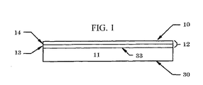
図面に戻ると、図1は、その上面33上に搭載されたメタライズされたフィルムまたは箔12を有する基板またはベース層11を有する、本発明による識別ユニット10の側面図を示す。基板11の下面30がまた示されている。示されるように、メタライズされたフィルムまたは箔12は、金属層14で被覆されたフィルム13を含む。フィルム13は、好ましくはポリマーフィルムなどの誘電体フィルムである。ポリエチレンテレフタレート(PET)が、フィルムに好ましい材料である。しかしながら、他の材料をフィルム13に使用することもできる。基板もまた、好ましくは誘電体材料である。しかしながら、基板11は、使用されるフィルム13のタイプに応じて、電気導電特性または誘電特性のいずれかを有する材料で作ることができる。例えば、フィルム13が、ポリマーフィルムなどの誘電体材料であるなら、基板11が誘電体材料である必要性はない。
Returning to the drawings, FIG. 1 shows a side view of an
図1に示される識別装置10は、カードまたは識別ラベルの形態であることができる。ラベルは、一般に識別カードより柔軟である。識別装置の剛性は、基板11に使用される材料の選択によって、および基板11の厚みによって変わることができる。
The
さらに、図1に示される識別装置10は、必ずしも実際の最終製品を表す必要はないが、図1に示される層に加えて、特に上部および下部を覆う層などのさらなる層を備えることができることに留意されたい。さらに、識別ユニットが識別ラベルとして構成されているなら、装置は、感圧接着剤面などの接着性表面を備えることができる。
In addition, the
図2は、本発明による識別装置10の平面図である。図2に示されるように、メタライズされた層12は、隣接した位置に配置された2つのフィールドに分割されている。すなわち、ホログラフィック画像フィールド16と、アンテナフィールド17である。ホログラフィックフィールド16において、金属フィルム12は、ホログラム20を形成するための公知の方法(例えば、打ち抜き法を使用して)で識別装置に転写することができるホログラフィック画像18を形成する。
FIG. 2 is a plan view of the
図2に示されるように、アンテナフィールド17は、例えば、本発明による化学的エッチング技術を使用することによって形成されるアンテナコイル22を備える。図示するコイルは、各端部に接触フィールド23および24を備える。接触フィールド23および24は、図3に示されるようにベース層11の底面30との電気的な接続を提供するスルーコンタクトとして提供される。
As shown in FIG. 2, the
図2に示されるアンテナコイル22の構成に関して、腐食性材料(すなわち、NaOH水溶液)を、金属層14上にプリントして、金属箔12から金属層18の部分を選択的に除去し、それによってアンテナコイル22として画定される区域だけを残すことができる。
With respect to the configuration of the
図3は、図2に示される装置の底面図を示す。図3に示されるように、アンテナコイル22の接触点23、24は、アンテナ22とチップ31との間の電気接触をより容易にするために示されるようにチップモジュール32に搭載される、基板11の底面30上のチップ31に対するスルーコンタクトとして接続される。
FIG. 3 shows a bottom view of the apparatus shown in FIG. As shown in FIG. 3, the contact points 23, 24 of the
図1から図3に示される識別装置10のアンテナコイル22およびチップ31は、トランスポンダユニット34を形成し、このトランスポンダユニット34は、読み取りユニットによって、電子的な識別の目的でチップ31のデータに対する接点の無いアクセスを可能にする。同時に、識別ユニット10の上面に搭載されたホログラム20は、光学的な識別がなされることを可能にする。
The
図4は、互いに上下に配置される2つの基板41、42を有する識別装置40を示し、各基板は、その上面43、44上に搭載されたメタライズされた箔45、46を有する。構成部品は、メタライズされた箔45が、基板41と42との間に配置され、メタライズされた箔46が、メタライズされた層41の上面43上に位置し、同時に識別装置40の上層を形成するように構成されている。図4に示されるように、各金属箔45、46は、メタライズされた表面39を有するフィルムまたは箔層47を備える。本発明の好ましい実施形態によれば、金属箔45、46は、アルミニウムを含むメタライズされた表面を有するポリマーフィルムを含む。
FIG. 4 shows an
図4に示される識別装置40において、上方金属箔46は、図2の金属箔12と同じ方法で構成または分割されている。換言すれば、識別装置40は、例えばホログラム区域16におけるホログラム20、ならびにアンテナ区域17におけるアンテナコイル22の両方を備える。示されるように、基板42の上面44上に搭載され、かつ基板42と基板41との間に配置される金属箔45は、接触点23、24を有するスルーコンタクトを介して、アンテナ区域17上に配置された第1のアンテナコイルと電気的に接触する第2のアンテナコイル49を備える。第2のアンテナコイル49は、それら自身が、基板42の底面におけるへこみ52に搭載されるチップモジュール53に接続される接触点50、51にスルーコンタクトによって自身が接続される。このように、アンテナコイル22および49は、それぞれ識別装置40の完全なアンテナコイルユニット54の構成部品を形成する。
In the
図5は、示されていない基板の上面上に金属箔56を備える識別装置55の平面図を示す。それぞれ図2および図4の金属箔12および46と同様な方法で、識別装置55が、例えば、ホログラムまたは逆反射区域57、あるいは他のメタライズされた物質、およびアンテナ区域58を備える。図5に示されるようなアンテナ区域58は、フィルムまたは箔層(図示されていない)上に被着された金属層61から作られる金属箔を選択的にエッチングすることによって、前述された方法で形成されることができる単一のアンテナコイル59を含む。示されるように、アンテナコイル59は、接触点62、63を備える。接触点62、63は、基板の底面上に搭載されたチップモジュール64の接触区域に接続されたスルーコンタクトとして設計することができる。
FIG. 5 shows a plan view of an
ホログラム、または金属箔56の他のメタライズされた区域57において、ホログラムまたは他の画像65が、前述された方法で金属層に形成される。しかしながら、図5に示されるように、ホログラムまたは他の金属材料65は、互いに電気的に絶縁された2つの画像セクション66、67を含み、これらのセクションは、見たとき、複雑な接続された光学的構造を形成する。小さい方の画像セクション67は、大きい方の画像セクション66から電気的に絶縁される。示されるように、小さい方の画像セクション67は、一般に2つのU字形状のアイランドとして見える2つの金属面を備える。図5に示されるように、各これらの金属表面は、接触区域62または63に接続され、かつコンデンサユニット70のパネル68、69を形成する。
In the hologram or other metallized
図6は、それぞれ図2、図4および図5に示される金属フィルム12、46、56と同様に、金属フィルム72を含む識別装置71を示す。示されるように、識別装置71はまた、同様にまたは代わりに、他のタイプの画像、または例えば逆反射材料、およびアンテナフィールド74を含むことができるホログラフィックフィールド73を含む。しかしながら、図2に示される金属フィルム12とは対照的に、金属フィルム12は、金属材料75のラインまたはストリップを有する網状の金属被覆である。結果として、画像は、金属フィールド77と1つおきにある非金属フィールド76から形成される。そのような構成は、前述の印刷/化学的なエッチング手順を用いて、アンテナコイル22と同じ方法を用いて形成することができる。特に、ホログラフィックフィールド73における連続する金属被覆は、連続する金属被覆上の化学的エッチング剤の印刷ラインによって網状にすることができる。結果として、網状のホログラフィック材料(すなわち、除去された金属材料の1つおきのラインまたはストリップを有する)を、形成することができる。
FIG. 6 shows an
図2と図6とを比較するとき、図6のホログラフィック材料78と図2のホログラフィック材料20との画像内容が類似していることを見ることができる。しかしながら、画像は異なる解像度を有する。特に、図6の画像は、ホログラフィック材料78の網状の構造のためにより低い解像度を有する。しかしながら、ホログラフィック材料78の網状構造は、RFエネルギーとの干渉を低減し、RFトランスポンダを識別装置71上に搭載することができるようにする。
When comparing FIG. 2 and FIG. 6, it can be seen that the image content of the
図7は、ホログラフィックまたは他のメタライズされたフィールドと、図2に示される金属箔12などのアンテナフィールドとを有する金属箔の製造方法を示す。特に、連続する順番で互いに接続された多数の箔セグメント26を有する金属箔ストリップ25が図7に示されている。金属箔ストリップ25が、切り取り点線27に沿って長手方向に分離されるとき、図2の金属箔12などの個々の金属箔セクションを提供することができる。
FIG. 7 shows a method for manufacturing a metal foil having a holographic or other metallized field and an antenna field such as the
図7に示されるように、金属箔ストリップ25は、走行方向28に、互いから連続して続く、示されるように中央の走行ライン29の左側および右側に配置された連続するホログラムまたは他のメタライズされた区域16と、アンテナ区域17とを含む。走行方向28において互いに続く1つの長いラインにおける、ホログラムまたは他のメタライズされた区域16およびアンテナ区域17の配設が、金属箔ストリップ25が走行方向28に前方に動くとき、ホログラムまたは他のメタライズされた区域16におけるホログラムまたは他のメタライズされた材料20と、アンテナ区域17におけるアンテナコイル22との連続的な製造を可能にする。さらに、金属箔ストリップ25の前方の移動は、様々な段階(段階I、IIおよびIIIとして図7に示されている)で、様々な操作を箔に実施することができるように段階的にすることができる。特に、金属箔ストリップ25上のアンテナ区域17は、段階Iで金属エッチング剤での印刷を受けることができる。腐食性材料の残りは、洗い落すことができ、一方、同時に金属層14の酸化区域は、段階IIで除去することができる。最後に、金属箔ストリップ25のアンテナ区域17を乾燥させることができる(段階III)。
As shown in FIG. 7, the metal foil strips 25 are continuous holograms or other metallizations arranged in the direction of
金属箔ストリップ25のアンテナ区域17におけるアンテナコイル22の製造に関して、ホログラフィックまたは他のメタライズされたフィールド16におけるメタライズされた層は、図7に示されるように選択的にデメタライズすることができる。さらに、ホログラフィックまたは他のメタライズされた材料20は、デメタライゼーション工程の後で、(例えば、回転するプレスによって)金属箔ストリップ25のホログラムまたは他の区域16に形成することができる。
With respect to the fabrication of the
図2に示される識別装置10を構成するために、ホログラムまたは他のメタライズされた区域16に形成されたホログラムまたは他のメタライズされた材料20と、アンテナ区域17に形成されたアンテナコイル22とを有する金属箔ストリップ25を、図示されていない基板上に配置し、(例えば接着剤で)積層し、分離ライン27に沿って分離して、図2に示される識別装置10などの個別の識別装置を提供することができる。
To construct the
次に、本発明によるデメタライジング工程を、より詳細に記載する。 Next, the demetalizing process according to the present invention will be described in more detail.
デメタライズされるべき区域が(例えば、グラフィックデザインを使用して)決定されると、ゴムの凹版(例えば、フレキソプレート)を製作して、フィルムのメタライズされた表面上にデメタライジング溶液(例えば、水酸化ナトリウムの水溶液)の被着するために使用される印刷ローラを覆うことができる。水酸化ナトリウム溶液は、例えば、従来のフレキソ印刷装置の1つの印刷ステーションに配置することができる。例えば、デメタライジング溶液は、インクを保持するために一般に使用されるステンレス鋼トレイに入れることができる。そして、デメタライジング溶液は、デメタライズされるメタライズされた表面の区域へ選択的に移されるように、印刷ローラによってメタライズされた表面に加えることができる。メタライズされたフィルム上に“印刷される”水酸化ナトリウムの量は、インクを使用する印刷の場合と同様に、例えば、印刷ローラ(すなわち、アニロックスローラ)およびインク塗布ローラの構造(すなわち解像度)によって、および印刷ローラ上に加えられる圧力によって、制御することができる。 Once the area to be demetalized is determined (eg, using graphic design), a rubber intaglio (eg, flexographic plate) is made to produce a demetalizing solution (eg, on the metallized surface of the film) The printing roller used to deposit the aqueous solution of sodium hydroxide) can be covered. The sodium hydroxide solution can be placed, for example, in one printing station of a conventional flexographic printing apparatus. For example, the demetalizing solution can be placed in a stainless steel tray that is commonly used to hold ink. The demetallizing solution can then be added to the metallized surface by the printing roller so that it is selectively transferred to the area of the metallized surface to be demetallized. The amount of sodium hydroxide “printed” on the metallized film depends on, for example, the construction of the printing roller (ie, anilox roller) and the ink application roller (ie, resolution), as in the case of printing using ink. , And the pressure applied on the printing roller.
デメタライジング作用は、デメタライジング溶液がメタライズされた表面に加えられた実質直後に起こるが、溶液と接触する区域で化学反応が完了するように、デメタライジング溶液が、所定の時間だけメタライズされる表面との接触を維持することを可能することが望ましいかもしれない。 The demetalizing action occurs immediately after the demetalizing solution is applied to the metallized surface, but the demetalizing solution is metallized for a predetermined time so that the chemical reaction is completed in the area where it contacts the solution. It may be desirable to be able to maintain contact with the surface being made.
溶液の酸化作用を停止するために、メタライズされた表面を水洗することができる(好ましくは再利用しない)。例えば、(事前に印刷された)メタライズされた表面は、残留する水酸化ナトリウムおよび酸化された金属(すなわち、酸化アルミニウム)を除去することができる洗浄区域に通すことができる。好ましい実施形態において、水は、メタライズされた表面の全ての印刷された区域を湿す。例えば、精密スプリンクラーを使用して全ての印刷された区域を覆うことができる。洗浄工程をより効率的にするために、かつ化学的工程の残留物を完全に取り除くために、洗浄は、毎回新しい水を使用しながら1回または複数回繰り返すこともできる。 In order to stop the oxidizing action of the solution, the metallized surface can be washed (preferably not reused). For example, the (pre-printed) metallized surface can be passed through a wash area where residual sodium hydroxide and oxidized metal (ie, aluminum oxide) can be removed. In a preferred embodiment, the water wets all printed areas of the metallized surface. For example, a precision sprinkler can be used to cover all printed areas. In order to make the washing process more efficient and to completely remove chemical process residues, the washing can also be repeated one or more times using fresh water each time.
フィルムが乾燥ステーションに入る前に、残留する残りの水の蒸発を容易にするために、メタライズされた表面から過剰な水を取り除くことが望ましいかもしれない。水を取り除くために、一対のローラ(例えば、一方がゴムで他方が金属)、エアークリーナ、スポンジおよび/または空気スプリンクラーを用いることが薦められる。最後に、熱乾燥(例えば、電気抵抗加熱を用いて)のためにフィルムを乾燥ユニットに通して材料から水を完全に取り除く。 It may be desirable to remove excess water from the metallized surface to facilitate evaporation of the remaining water before the film enters the drying station. To remove water, it is recommended to use a pair of rollers (eg, one rubber and the other metal), air cleaner, sponge and / or air sprinkler. Finally, the film is passed through a drying unit for heat drying (eg, using electrical resistance heating) to completely remove water from the material.
選択的なデメタライジング方法の補足として、インクでの重ね印刷工程を同じ製造ラインに含めることが可能である。このように、同じ材料でデメタライジングおよび印刷の作用を得ることができる。 As a supplement to the selective demetalizing method, an ink overprinting process can be included in the same production line. In this way, demetalizing and printing effects can be obtained with the same material.
溶剤ベースのインクと比較して、水ベースのインクは、非常に扱いやすく、清浄であり、かつ紫外線(UV)光に対して非常に耐性がある。これらの理由のために、水ベースのインクが望ましい。それにもかかわらず、デメタライジング工程の1つの副工程が洗浄であるため、デメタライジングステップおよび洗浄ステップが完了した後、水ベースのインクで印刷することが好ましい。 Compared to solvent-based inks, water-based inks are very easy to handle, clean, and very resistant to ultraviolet (UV) light. For these reasons, water-based inks are desirable. Nevertheless, since one sub-step of the demetalizing process is washing, it is preferable to print with water-based ink after the demetalizing and washing steps are completed.
さらに、所定のメタライズされた区域が印刷されないことが望ましいなら、メタライズされたフィルムを保護する印刷として、透明な溶剤ベースのワニスを使用することが可能である。印刷保護の後、メタライズされた層をデメタライズすることができる。このように、より高い解像度を達成することができる。この技術は、微細な文字および/または非常に微細なラインを作成するために、高いセキュリティを要する用途で使用することができる。 Furthermore, if it is desired that a given metallized area is not printed, it is possible to use a clear solvent-based varnish as a print that protects the metallized film. After print protection, the metallized layer can be demetallized. In this way, higher resolution can be achieved. This technique can be used in high security applications to create fine characters and / or very fine lines.
本発明による逆反射材料などのメタライズされた材料とで使用するデメタライジング工程を、図8を参照して以下に記載する。第1に、金属層83上に存在するライナまたは保護層81を除去して、金属を露出させる。図8において、金属層132が、キャリアまたはベース層78上に配置された状態で示されている。キャリアまたはベース層78は、ポリ塩化ビニルまたはポリエチレンテレフタレートであることができる。そして、金属層132を、所望の区域から金属を除去するために、フレキソ、スクリーン、オフセットまたは他の印刷工程を用いて、水酸化ナトリウム溶液などの腐食性材料の腐食作用に選択的にさらす(79)。この工程は、メキシコ特許出願第2001/010968号および第2001/010969号、ならびにドイツ国特許出願第10121126号に詳細に記載されている。これらの出願全体を引用例として本明細書に組み込む。選択的な金属除去は、RFトランスポンダのためのアンテナを形成するために使用することができる。
A demetalizing process for use with a metallized material such as a retroreflective material according to the present invention is described below with reference to FIG. First, the liner or
第2のステップとして、同じデメタライジング工程を使用して微細なラインのデメタライジング工程を残留する金属表面上で実施して、金属層の導電性および無線波の吸収または歪みを断つことができる。これが、RFエネルギーを無線周波数装置のアンテナによって捉えられることを可能にする。この工程は、好ましくは、残留する金属層の逆反射(すなわち、例えばホログラフィック)特性を維持するために高解像度で行われ、一方、同時にRF受信および送信を可能にするように金属の導電性を遮断する。 As a second step, using the same demetalizing process, a fine line demetalizing process may be performed on the remaining metal surface to break the conductivity and radio wave absorption or distortion of the metal layer. it can. This allows RF energy to be captured by the antenna of the radio frequency device. This step is preferably performed at a high resolution to maintain the retroreflective (ie, holographic, for example) properties of the remaining metal layer, while at the same time conducting the metal to allow RF reception and transmission. Shut off.
本発明の好ましい実施形態によれば、メタライズされた層は、第2の組の平行ラインまたはデメタライズされた材料に対して直角に向けられたデメタライズされた材料の第1の組の平行ラインを備える方形格子パターンでデメタライズされる。本発明のさらなる実施形態によれば、方形格子パターンにおけるメタライズされた材料の方形は、5mm×5mm以下、より好ましくは3mm×3mm以下の寸法を有する。メタライズされた材料の方形が約5mm以下の寸法を有するとき、シールド率(すなわち、歪みおよび/または吸収)が約5%以下に低減し、メタライズされた材料の方形が、約3mm以下の寸法を有するとき、シールド率(すなわち、歪みおよび/または吸収)が約1%以下に低減することが見出された。 According to a preferred embodiment of the invention, the metallized layer comprises a second set of parallel lines or a first set of parallel lines of demetalized material oriented at right angles to the demetalized material. Demetallized with a square lattice pattern. According to a further embodiment of the invention, the square of the metallized material in the square lattice pattern has a dimension of 5 mm x 5 mm or less, more preferably 3 mm x 3 mm or less. When the square of the metallized material has a dimension of about 5 mm or less, the shielding rate (ie, strain and / or absorption) is reduced to about 5% or less, and the square of the metallized material has a dimension of about 3 mm or less. When having, it has been found that the shielding rate (ie, strain and / or absorption) is reduced to about 1% or less.
方形格子状のデメタライズされたパターンが好ましいが、他のパターンを本発明にしたがって用いることもできる。他のパターンが用いられるとき、メタライズされた区域上に描かれることができる最も長い直線ラインが、約5mm以下、より好ましくは3mm以下であることが好ましい。 A square grid demetallized pattern is preferred, but other patterns may be used in accordance with the present invention. When other patterns are used, it is preferred that the longest straight line that can be drawn on the metallized area is about 5 mm or less, more preferably 3 mm or less.
メタライズされた材料のロールの選択的なデメタライゼーションのための装置の概略が図9に示されている。図9に示されるように、ロール121からメタライズされた材料(例えば逆反射材料)が巻き戻され、印刷ローラ123に通され、そこでリザーバ35から化学的エッチング剤(例えば、NaOH)が所望のパターンで加えられる。そして、印刷されたメタライズされた層は、温度印加ローラ128を超えて洗浄ステーション36へ通過する。洗浄後、ドライヤ37からの高温空気が、洗浄された材料の表面上へ向けられる。その後、場合によっては、選択的にデメタライズされた材料は様々な印刷ステーション38、120へ移され、デザインをその上に重ね印刷することができる。重ね印刷後、メタライズされた材料は、接着剤塗布ローラ122へ移され、キャリア材料またはベース層材料124に接着結合されることができる。ベース層材料124は、連続する長い材料から個別の識別装置の分離を可能にするために、貫通孔(図示されていない)を有することができる。ベース層への結合後、材料は、テイクオフローラ126に巻かれた状態で示されている。
A schematic of an apparatus for selective demetallization of a roll of metallized material is shown in FIG. As shown in FIG. 9, the metallized material (eg, retroreflective material) from
材料をデメタライゼーション剤にさらした後、水で表面を洗浄しかつ直ちに乾燥することによってデメタライゼーション工程を終了させることができる。その後、固定または可変の印刷工程を使用してデザインを識別装置上に重ね印刷することができる。 After exposing the material to a demetallization agent, the demetallization process can be terminated by washing the surface with water and immediately drying. The design can then be overprinted on the identification device using a fixed or variable printing process.
金属が装置の区域から除去されると、デメタライズされた区域に無線周波数装置を搭載することができる。無線周波数装置は、車両免許プレートなどのラベルまたは識別タグとして使用することができる。 Once the metal is removed from the area of the device, the radio frequency device can be mounted in the demetallized area. The radio frequency device can be used as a label or identification tag such as a vehicle license plate.
ある例示的な適用において、本発明によるラベルは、例えば、全てのタイプの車両制御に使用することができる。ラベルは、自動車免許プレート、トラクタプラットフォームでの使用のために、またはコンテナ情報、車両制御用途などのために自動接着剤形態で提供することができる。ラベルは、読み取りおよび書き込み能力を備えることができ、また指紋、虹彩認識データ、顔面認識データ、音声認識データ、写真データなどの生物測定データ、および運転手に関する交通違反データを含むことができる。 In certain exemplary applications, the labels according to the invention can be used, for example, for all types of vehicle control. The label can be provided in an auto-adhesive form for use on automobile license plates, tractor platforms, or for container information, vehicle control applications, and the like. The label can have read and write capabilities and can include biometric data such as fingerprints, iris recognition data, face recognition data, voice recognition data, photographic data, and traffic violation data for the driver.
自動車免許プレートは、一般に金属、アクリルまたはポリカーボネートから作ることができる。材料に係わらず、RF装置を加える工程は通常類似する。この工程を、金属免許プレートに関して図10を参照して以下に記載する。第1に、金属プレート80の上面82をエンボス加工して、くぼんだ領域84を形成する。次に、絶縁層86(例えばフェライト複合物層)をくぼんだ領域84に取り付ける。そして、無線周波数装置88を絶縁層に取り付ける。このように、RF装置88は、金属プレート80からの干渉なしに情報を送信および受信することができる。その後、免許プレートを、例えば選択的にデメタライズされた逆反射材料90とで積層することができる。本発明の好ましい実施形態によれば、無線周波数装置88が搭載される区域92上の逆反射材料90の領域は、メタライズされた材料がない。さらに、逆反射材料90の残りは、好ましくは、干渉を低減するために、上述のデメタライゼーション工程を使用して、微細なラインのデメタライゼーションパターン93で選択的にデメタライズされる。
Automobile license plates can generally be made from metal, acrylic or polycarbonate. Regardless of the material, the process of adding an RF device is usually similar. This process is described below with reference to FIG. 10 for the metal license plate. First, the
得られる免許プレートを図11に示す。図11から分かるように、免許プレート94は、アンテナ領域96および逆反射領域98を含む。逆反射領域は、免許プレート番号とともに重ね印刷された状態で示されている。図11から分かるように、逆反射材料は、アンテナ領域96から除去されている。アンテナは、上述された印刷手順を使用して、連続する金属層を選択的にデメタライジングすることによって形成することができる。
The resulting license plate is shown in FIG. As can be seen from FIG. 11, the
アンテナを形成する代わりの工程は、埋め込まれたアンテナ(好ましくは銅アンテナ)を有する薄いポリマー層(例えば、ポリ塩化ビニル(PVC)またはポリエチレンテレフタレート)の製造を含む。このタイプの構造は、一般にインレーと呼ばれる。本発明によるはめ込みアンテナの製造方法が図12に示されている。図12に示されるように、導電ワイヤ100(好ましくは銅ワイヤ)をスプール102から巻き戻し、ポリマーシート104の表面に埋め込む。図12に示されるように、導電ワイヤ100は、加熱超音波ヘッド106上を超えかつブリッジ108下を通過したのち、ポリマーシート104に埋め込まれてアンテナ110を形成する。はめ込まれたアンテナに、識別装置のベース層または基板に対する自動接着剤または感圧接着剤を付けることができる。アンテナは、識別装置の金属との接触を避けるためにデメタライズされている装置の区域に付けなければならない。
An alternative process of forming the antenna involves the manufacture of a thin polymer layer (eg, polyvinyl chloride (PVC) or polyethylene terephthalate) with an embedded antenna (preferably a copper antenna). This type of structure is commonly referred to as an inlay. A method for manufacturing a telescoping antenna according to the invention is shown in FIG. As shown in FIG. 12, the conductive wire 100 (preferably copper wire) is unwound from the
金属プレートまたはスティッカ上に逆反射または他のメタライズされた材料を得るための、キャリアまたはベース層がPVCまたはPETなどのポリマーである代わりの方法を用いることができる。この実施形態において、アンテナは、上記に示された超音波エネルギーを使用してキャリアに直接埋め込むことができる。そして、逆反射または他のメタライズされた層をキャリア上に付けることができる。アンテナを覆う逆反射または他のメタライズされた層の部分は、逆反射または他のメタライズされた材料の含有金属とのアンテナの接触を避けるために、デメタライズされるべきである。微細なラインのデメタライゼーション工程を、無線周波数装置と干渉することがあるRF歪みまたは吸収を最小化するために、逆反射または他のメタライズされた材料の残りに対して上述のように使用することができる。その後で、アクリルまたはエポキシ樹脂を塗布して、識別装置をラベルに変えることができる。 Alternative methods for obtaining a retroreflective or other metallized material on a metal plate or sticker where the carrier or base layer is a polymer such as PVC or PET can be used. In this embodiment, the antenna can be directly embedded in the carrier using the ultrasonic energy indicated above. A retroreflective or other metallized layer can then be applied over the carrier. The portion of the retroreflective or other metallized layer that covers the antenna should be demetallized to avoid antenna contact with the retroreflective or other metallized material containing metal. A fine line demetallization process is used as described above for retroreflective or other metallized material remnants to minimize RF distortion or absorption that may interfere with radio frequency equipment. be able to. Thereafter, acrylic or epoxy resin can be applied to turn the identification device into a label.
図13は、はめ込まれたアンテナ110が、逆反射または他のメタライズされた層114のデメタライズされた部分112の下のキャリア層(図示されていない)に配置される、本発明のこの実施形態による識別装置を示す。同じく図13に示されるように、微細なラインのデメタライゼーション工程を逆反射層114の連続する金属部分116に用いて、干渉を低減し、それによって無線周波数送信118および受信119機能の適切な性能を保証している。このように、RFエネルギーの適切な送信および受信を可能にしながらも逆反射または他のメタライズされた材料特性を維持することができる。
FIG. 13 shows that an embedded
本発明に対するこれらおよび他の修正および変形は、本発明の本質および範囲を逸脱することなく、当業者によって実行することができる。さらに当業者は、前述の記載が、例示だけを目的とするものであり、本発明を限定するものではないことを理解するであろう。 These and other modifications and variations to the present invention can be made by those skilled in the art without departing from the essence and scope of the present invention. Moreover, those skilled in the art will appreciate that the foregoing description is for illustrative purposes only and is not intended to limit the invention.
Claims (66)
ベース層と、
無線周波数(RF)チップ、およびチップと電気的に通信しており、ベース層上に配置されたアンテナを備えるRFトランスポンダと、
断続的にメタライズされた領域とを備え、
断続的にメタライズされた領域が、RFトランスポンダが無線周波数で情報を送信および受信することを可能にする識別装置。 An identification device,
The base layer,
An RF transponder comprising a radio frequency (RF) chip and an antenna in electrical communication with the chip and disposed on the base layer;
With intermittent metallized areas,
An identification device in which intermittently metallized regions allow RF transponders to transmit and receive information at radio frequencies.
印刷法を用いて、メタライズされた領域の露出面の部分に金属エッチング溶液を移すことと、
エッチング溶液をメタライズされた領域と反応させて、表面を選択的にデメタライズすることと、
選択的にデメタライズされた表面を洗浄することとを含む方法。 A method of forming a pattern in a metallized area,
Using a printing method to transfer the metal etching solution to the exposed surface portion of the metallized area;
Reacting the etching solution with the metallized areas to selectively demetallize the surface;
Cleaning the selectively demetallized surface.
第1のメタライズされた領域にアンテナを形成することと、
第2のメタライズされた領域にホログラフィック画像を形成することとを含み、
アンテナが、
印刷法を用いて、メタライズされた層の露出面の部分に金属エッチング溶液を移すことと、
エッチング溶液を金属と反応させて、表面を選択的にデメタライズすることと、
選択的にデメタライズされた表面を洗浄することとを含む方法によって形成される方法。 A method of manufacturing an identification device comprising a base layer and a plurality of metallized regions disposed on the base layer,
Forming an antenna in the first metallized region;
Forming a holographic image in a second metallized region;
The antenna is
Using a printing method to transfer the metal etching solution to the exposed portion of the metallized layer;
Reacting the etching solution with a metal to selectively demetallize the surface;
Cleaning the selectively demetallized surface.
ベース層上にアンテナを形成することと、
アンテナと電気的に通信している無線周波数(RF)チップをベース層上に搭載してRFトランスポンダを形成することとを含み、
アンテナが、連続してメタライズされた層の選択的なデメタライゼーションによって、または断続的にメタライズされた層の部分的な被着によって形成される方法。 A method of manufacturing a radio frequency (RF) identification device comprising:
Forming an antenna on the base layer;
Mounting a radio frequency (RF) chip in electrical communication with the antenna on the base layer to form an RF transponder;
A method wherein the antenna is formed by selective demetallization of successive metallized layers or by partial deposition of intermittent metallized layers.
印刷法を用いて、連続してメタライズされた層の露出面の部分に金属エッチング溶液を移すことと、
エッチング溶液を金属と反応させることと、
メタライズされた層の露出面を洗浄することとを含む、請求項30に記載の方法。 The antenna is formed by selective demetallization of successive metallized layers, and the selective demetallization is
Using a printing method to transfer the metal etching solution to the exposed surface portion of the continuously metallized layer;
Reacting the etching solution with the metal;
31. The method of claim 30, comprising cleaning the exposed surface of the metallized layer.
ベース層上に断続的な逆反射層を形成することと、
ベース層上にアンテナを形成することと、
ベース層上に無線周波数(RF)チップを搭載することとを含み、
チップとアンテナとが電気的に通信してRFトランスポンダを形成し、RFトランスポンダが無線周波数で情報を送信および受信することを許しながら、断続的な逆反射層が逆反射特性を維持する方法。 A method of manufacturing an identification device comprising a base layer and a metallized retroreflective layer, comprising:
Forming an intermittent retroreflective layer on the base layer;
Forming an antenna on the base layer;
Mounting a radio frequency (RF) chip on the base layer,
A method in which an intermittent retroreflective layer maintains retroreflective properties while the chip and antenna are in electrical communication to form an RF transponder, allowing the RF transponder to transmit and receive information at radio frequencies.
ポリマー層に導電ワイヤを埋め込むことによってはめ込みアンテナを形成することと、
ベース層にはめ込みアンテナを取り付けることとを含む、請求項35に記載の方法。 Forming an antenna,
Forming a telescoping antenna by embedding a conductive wire in the polymer layer;
36. The method of claim 35, comprising attaching a telescoping antenna to the base layer.
接着剤層を介してアンテナを装置に接着結合することを含む、請求項37に記載の方法。 An adhesive layer is provided for the inset antenna, further mounting the antenna,
38. The method of claim 37, comprising adhesively bonding the antenna to the device via an adhesive layer.
くぼんだ領域に絶縁層を形成することとを含み、
無線周波数(RF)チップが絶縁層上に搭載される、請求項35に記載の方法。 In addition, forming a recessed region in the base layer;
Forming an insulating layer in the recessed area;
36. The method of claim 35, wherein a radio frequency (RF) chip is mounted on the insulating layer.
印刷法を用いて、連続してメタライズされた逆反射層の露出面の部分に金属エッチング溶液を移すことと、
エッチング溶液を逆反射層の金属と反応させることと、
メタライズされた逆反射層の露出面を洗浄することとを含む、請求項35に記載の方法。 Forming an intermittent retroreflective layer,
Using a printing method to transfer the metal etching solution to the exposed surface portion of the continuously metallized retroreflective layer;
Reacting the etching solution with the metal of the retroreflective layer;
36. The method of claim 35, comprising cleaning an exposed surface of the metallized retroreflective layer.
ベース層に導電ワイヤを埋め込むことによってはめ込みアンテナを形成することを含む、請求項35に記載の方法。 The base layer comprises a polymer material to form an antenna;
36. The method of claim 35, comprising forming a telescoping antenna by embedding a conductive wire in the base layer.
ベース層と、
無線周波数(RF)チップ、およびチップと電気的に通信しており、ベース層上に配置されたアンテナを備えるRFトランスポンダとを含み、
アンテナが、連続してメタライズされた層の選択的なデメタライゼーションによって、または断続的にメタライズされた層の部分的な被着によって形成されている識別装置。 An identification device,
The base layer,
A radio frequency (RF) chip and an RF transponder in electrical communication with the chip and comprising an antenna disposed on the base layer;
An identification device in which the antenna is formed by selective demetallization of successive metallized layers or by partial deposition of intermittent metallized layers.
Applications Claiming Priority (9)
| Application Number | Priority Date | Filing Date | Title |
|---|---|---|---|
| DE10121126A DE10121126A1 (en) | 2001-04-30 | 2001-04-30 | Identification medium and process for its production |
| MXPA01010967 MXPA01010967A (en) | 2001-10-26 | 2001-10-26 | Dematallizing process of holographic plastic particles. |
| MXPA01010969 MXPA01010969A (en) | 2001-10-26 | 2001-10-26 | Reflective material device and obtaining process. |
| MXPA01010968 MXPA01010968A (en) | 2001-10-26 | 2001-10-26 | Demetallized process of reflective plastic particles. |
| MXPA01010971A MXPA01010971A (en) | 2001-04-30 | 2001-10-26 | Holographic material device having a chip and an integrated antenna, and a process for obtaining the same. |
| MXPA02003141 MXPA02003141A (en) | 2002-03-25 | 2002-03-25 | Process for obtaining a device of a retro reflective material of pvc or pet with a radio frequency device. |
| MXPA02003202 MXPA02003202A (en) | 2002-03-26 | 2002-03-26 | Process for obtaining a device of a retro reflective material with a radio frequency device. |
| US10/118,092 US7034688B2 (en) | 2001-04-30 | 2002-04-09 | Selective metal removal process for metallized retro-reflective and holographic films and radio frequency devices made therewith |
| PCT/IB2002/001439 WO2002089338A2 (en) | 2001-04-30 | 2002-04-30 | Selective metal removal process for metallized retro-reflective and holographic films and radio frequency devices made therewith |
Publications (2)
| Publication Number | Publication Date |
|---|---|
| JP2005513585A true JP2005513585A (en) | 2005-05-12 |
| JP2005513585A5 JP2005513585A5 (en) | 2005-12-22 |
Family
ID=33136388
Family Applications (1)
| Application Number | Title | Priority Date | Filing Date |
|---|---|---|---|
| JP2002586510A Pending JP2005513585A (en) | 2001-04-30 | 2002-04-30 | Selective metal removal method for metallized retroreflective and holographic films and radio frequency device produced by the method |
Country Status (8)
| Country | Link |
|---|---|
| US (1) | US7463154B2 (en) |
| EP (3) | EP1405278B1 (en) |
| JP (1) | JP2005513585A (en) |
| AT (1) | ATE480843T1 (en) |
| AU (1) | AU2002255218A1 (en) |
| DE (1) | DE60237606D1 (en) |
| MX (1) | MXPA03009959A (en) |
| WO (1) | WO2002089338A2 (en) |
Cited By (8)
| Publication number | Priority date | Publication date | Assignee | Title |
|---|---|---|---|---|
| JP2009544111A (en) * | 2006-07-18 | 2009-12-10 | ジェイディーエス ユニフェイズ コーポレーション | Protective measures by demetalization of holographic magnetic stripes |
| JP2010055467A (en) * | 2008-08-29 | 2010-03-11 | Toppan Printing Co Ltd | Rfid label with optical function |
| JP2010160683A (en) * | 2009-01-08 | 2010-07-22 | Toppan Printing Co Ltd | Optical variable device having ic tag inlet |
| JP2011134048A (en) * | 2009-12-24 | 2011-07-07 | Toppan Printing Co Ltd | Antenna sheet and booklet body with ic |
| US8052171B2 (en) | 2004-06-30 | 2011-11-08 | Ovd Kinegram Ag | Security element for RF identification |
| JP2017003619A (en) * | 2015-06-04 | 2017-01-05 | 凸版印刷株式会社 | Sealing sticker |
| KR20180078157A (en) * | 2016-12-29 | 2018-07-09 | 더 스와치 그룹 리서치 앤 디벨롭먼트 엘티디 | Portable object comprising a near-field connection device |
| WO2021199460A1 (en) * | 2020-03-30 | 2021-10-07 | 住友理工株式会社 | Film antenna and method for producing film antenna |
Families Citing this family (50)
| Publication number | Priority date | Publication date | Assignee | Title |
|---|---|---|---|---|
| DE10121126A1 (en) * | 2001-04-30 | 2002-11-07 | Intec Holding Gmbh | Identification medium and process for its production |
| DE10232007A1 (en) | 2002-07-15 | 2004-02-19 | Giesecke & Devrient Gmbh | Transponder for flat-shaped articles |
| AU2003288687A1 (en) * | 2002-11-22 | 2004-06-18 | Bnc Ip Switzerland Gmbh | Radio frequency identification device formed in a non-metallized region with an antenna connected to an outside metallized region, and method of manufacturing |
| EP1468619B1 (en) * | 2003-04-17 | 2006-10-18 | Industria Bergamasca Rifrangenti S.r.l. | Method for producing printed retroreflective high visibility products |
| GB0326576D0 (en) | 2003-11-14 | 2003-12-17 | Printetch Ltd | Printing composition |
| KR20070085841A (en) | 2004-11-08 | 2007-08-27 | 프레쉬포인트 홀딩스 에스아 | Time-temperature indicating device |
| GB0427664D0 (en) * | 2004-12-16 | 2005-01-19 | Forshaw Guy | Identification system |
| US7323977B2 (en) * | 2005-03-15 | 2008-01-29 | Intermec Ip Corp. | Tunable RFID tag for global applications |
| WO2007054264A1 (en) * | 2005-11-08 | 2007-05-18 | Joergen Brosow | Areal substrate for recording information and method for producing the substrate |
| DE102006025485B4 (en) * | 2006-05-30 | 2008-03-20 | Polylc Gmbh & Co. Kg | Antenna arrangement and its use |
| US8236220B2 (en) * | 2006-08-16 | 2012-08-07 | High Impact Technology, Llc | Method of making an embedded-object and composite-material product |
| GB2441013A (en) * | 2006-08-19 | 2008-02-20 | Curtis Consulting Ltd | A sign, in particular a vehicle number plate, incorporating an RFID device and an antenna for the RFID device. |
| AU2007317875B2 (en) | 2006-11-06 | 2014-03-06 | Josef Feldman | Laminated identification document |
| EP2131217A4 (en) * | 2007-03-01 | 2010-11-03 | Nippon Carbide Kogyo Kk | Radio wave transmission type retroreflection sheet |
| KR20090017870A (en) * | 2007-08-16 | 2009-02-19 | 삼성광주전자 주식회사 | Suction brush for vacuum cleaner having hair removal unit |
| DE102007041752A1 (en) * | 2007-09-04 | 2009-03-05 | Bielomatik Leuze Gmbh + Co Kg | Chip module for an RFID system |
| PL2192530T3 (en) * | 2007-09-14 | 2013-08-30 | Toppan Printing Co Ltd | Antenna sheet, transponder and booklet |
| AU2009256212B2 (en) * | 2008-06-04 | 2015-12-10 | Jp Laboratories Inc. | A monitoring system based on etching of metals |
| JP2008276799A (en) * | 2008-07-08 | 2008-11-13 | Dainippon Printing Co Ltd | Optical diffraction ic tag label |
| FR2938095B1 (en) * | 2008-11-03 | 2012-12-21 | Oberthur Technologies | METHOD FOR INCREASING THE GAIN OF A PLANAR ANTENNA, IN PARTICULAR FOR A MICROCIRCUIT BOARD. |
| US8628679B2 (en) * | 2010-01-20 | 2014-01-14 | Phoenix Inks And Coatings, Llc | High-definition demetalization process |
| EA017569B1 (en) * | 2010-10-20 | 2013-01-30 | Республиканское Унитарное Предприятие "Минская Печатная Фабрика" Гознака | Method of formation of pattern on the surface of aluminized polymeric rolled material and etching solution therefor |
| TWI459418B (en) | 2012-03-23 | 2014-11-01 | Lg伊諾特股份有限公司 | Wireless power receiver and portable terminal comprising the same |
| JP6313744B2 (en) | 2012-03-23 | 2018-04-18 | エルジー イノテック カンパニー リミテッド | Wireless power receiver |
| DE102012106594A1 (en) * | 2012-07-20 | 2014-01-23 | J.H. Tönnjes E.A.S.T. GmbH & Co. KG | Vehicle identification means |
| AU2013231074A1 (en) * | 2012-10-08 | 2014-04-24 | Taxi Club Pty Ltd | Transport service card and system and method for facilitating a transport service |
| CA2896549A1 (en) | 2012-12-29 | 2014-07-03 | Meps Real-Time, Inc. | System and method of optimizing the process of identifying items tagged with rfid tags in an enclosed shielded space |
| TWI553732B (en) * | 2013-01-25 | 2016-10-11 | 矽品精密工業股份有限公司 | Electronic package structure |
| EP2851876A3 (en) * | 2013-09-19 | 2015-07-08 | Taxi Club Pty Ltd | Transport service card and system and method for facilitating a transport service |
| US9761945B2 (en) * | 2013-10-18 | 2017-09-12 | Taoglas Group Holdings Limited | Ultra-low profile monopole antenna for 2.4GHz band |
| US9917654B2 (en) | 2014-10-10 | 2018-03-13 | Richard Michael Hassler | Chip for transdermal emission or augmentation of energy |
| US10135148B2 (en) * | 2014-01-31 | 2018-11-20 | Kymeta Corporation | Waveguide feed structures for reconfigurable antenna |
| KR101762778B1 (en) | 2014-03-04 | 2017-07-28 | 엘지이노텍 주식회사 | Wireless communication and charge substrate and wireless communication and charge device |
| CN104062695A (en) * | 2014-03-20 | 2014-09-24 | 台州市万创夜光明工贸有限公司 | Method for manufacturing environment-friendly reflective fabric |
| CN104062698A (en) * | 2014-03-20 | 2014-09-24 | 台州市万创夜光明工贸有限公司 | Production method for high-intensity reflective films |
| KR20170065591A (en) | 2014-09-30 | 2017-06-13 | 쓰리엠 이노베이티브 프로퍼티즈 캄파니 | Retroreflective colored articles |
| US9688202B2 (en) | 2014-10-29 | 2017-06-27 | Neology, Inc. | Radio frequency identification enabled mirrors |
| EP3281153B1 (en) | 2015-04-07 | 2021-11-10 | Neology, Inc. | Radio frequency identification tag in a license plate |
| EP3329428B1 (en) | 2015-08-01 | 2021-12-01 | Smartrac Technology Fletcher, Inc. | Detachable radio frequency identification switch tag |
| EP3328692B1 (en) | 2015-08-01 | 2020-05-27 | Neology, Inc. | License plate validation |
| MX2017012620A (en) | 2015-08-01 | 2018-08-15 | Neology Inc | Self declaring device for a vehicle using restrict traffic lanes. |
| EP3733459B1 (en) | 2015-09-03 | 2022-02-09 | Neology, Inc. | Self-declaring electronic license plate |
| FR3042847B1 (en) * | 2015-10-23 | 2019-04-12 | Valeo Vision | LUMINOUS MODULE FOR A MOTOR VEHICLE WITH ELECTRONIC BIN ENCODING |
| CA3019902C (en) * | 2016-03-16 | 2022-06-21 | Ncc Nano, Llc | Method for depositing a functional material on a substrate |
| WO2017172888A1 (en) | 2016-03-30 | 2017-10-05 | 3M Innovative Properties Company | Article featuring a predetermined pattern of randomly distributed microspheres and methods of making the same |
| US10891530B2 (en) | 2018-11-07 | 2021-01-12 | Neology, Inc. | Detachable radio frequency identification switch tag |
| WO2020168375A1 (en) | 2019-02-18 | 2020-08-27 | Licensys Australasia Pty Ltd | A vehicle license plate |
| EP3977336A1 (en) * | 2019-05-24 | 2022-04-06 | 3M Innovative Properties Company | Radar-optical fusion article and system |
| DE102019127776A1 (en) * | 2019-08-14 | 2021-03-04 | Vacuumschmelze Gmbh & Co. Kg | Amorphous metal tape and a method for making an amorphous metal tape |
| US20210158125A1 (en) * | 2019-11-26 | 2021-05-27 | Avery Dennison Retail Information Services, Llc | Rfid devices including embossed or other elements |
Family Cites Families (30)
| Publication number | Priority date | Publication date | Assignee | Title |
|---|---|---|---|---|
| US3220899A (en) * | 1962-08-23 | 1965-11-30 | Litho Chemical & Supply Co Inc | Process for chemically graining lithographic plates |
| US4682852A (en) * | 1984-07-23 | 1987-07-28 | Victor Weber | Reflective sheeting technology |
| CA1242796A (en) * | 1984-10-12 | 1988-10-04 | Yoshihiro Kitsuda | Microwave plane antenna |
| US4610755A (en) * | 1985-04-16 | 1986-09-09 | Beckett Donald E | Demetallizing method |
| US4727360A (en) * | 1985-09-13 | 1988-02-23 | Security Tag Systems, Inc. | Frequency-dividing transponder and use thereof in a presence detection system |
| JPH01147078A (en) * | 1987-12-02 | 1989-06-08 | Ricoh Co Ltd | Etching ink composition for forming transparent electrode pattern and method for using same |
| US5046792A (en) * | 1989-12-13 | 1991-09-10 | Britton Zabka | Holographic printer |
| US5115182A (en) * | 1990-04-23 | 1992-05-19 | Motorola, Inc. | Battery charging controller for a battery powered device and method for using the same |
| US5396559A (en) * | 1990-08-24 | 1995-03-07 | Mcgrew; Stephen P. | Anticounterfeiting method and device utilizing holograms and pseudorandom dot patterns |
| DE69220029T2 (en) * | 1992-02-05 | 1997-09-18 | Texas Instruments Inc | Method for producing a flat, flexible antenna core for a chip transponder, built into a card or similar object, and an antenna core produced in this way |
| US5557279A (en) * | 1993-09-28 | 1996-09-17 | Texas Instruments Incorporated | Unitarily-tuned transponder/shield assembly |
| JP3305843B2 (en) * | 1993-12-20 | 2002-07-24 | 株式会社東芝 | Semiconductor device |
| US5621571A (en) * | 1994-02-14 | 1997-04-15 | Minnesota Mining And Manufacturing Company | Integrated retroreflective electronic display |
| US5682143A (en) * | 1994-09-09 | 1997-10-28 | International Business Machines Corporation | Radio frequency identification tag |
| US5528222A (en) * | 1994-09-09 | 1996-06-18 | International Business Machines Corporation | Radio frequency circuit and memory in thin flexible package |
| EP0704928A3 (en) * | 1994-09-30 | 1998-08-05 | HID Corporation | RF transponder system with parallel resonant interrogation and series resonant response |
| US5477219A (en) * | 1995-03-30 | 1995-12-19 | Minnesota Mining And Manufacturing Company | Composite electronic article surveillance, identification, and security marker assembly and system |
| US5945938A (en) * | 1996-11-14 | 1999-08-31 | National University Of Singapore | RF identification transponder |
| TW350054B (en) * | 1996-11-29 | 1999-01-11 | Mitsubishi Materials Corp | Burglarproof label |
| CH691098A5 (en) | 1997-03-24 | 2001-04-12 | Em Microelectronic Marin Sa | monolithic structure of integrated circuit and antenna coil provided with a peripheral protective ring. |
| WO1999008245A1 (en) * | 1997-08-08 | 1999-02-18 | Ird A/S | Polymeric radio frequency resonant tags and method for manufacture |
| US5973600A (en) * | 1997-09-11 | 1999-10-26 | Precision Dynamics Corporation | Laminated radio frequency identification device |
| US6608911B2 (en) * | 2000-12-21 | 2003-08-19 | Digimarc Corporation | Digitally watermaking holograms for use with smart cards |
| US6018299A (en) * | 1998-06-09 | 2000-01-25 | Motorola, Inc. | Radio frequency identification tag having a printed antenna and method |
| AU4708399A (en) | 1998-06-23 | 2000-01-10 | Trustees Of Boston University | Crystallographic wet chemical etching of iii-nitride material |
| JP2000085278A (en) | 1998-09-07 | 2000-03-28 | Konica Corp | Security card, method and device for its manufacture |
| US6203952B1 (en) | 1999-01-14 | 2001-03-20 | 3M Innovative Properties Company | Imaged article on polymeric substrate |
| US6222453B1 (en) * | 1999-03-24 | 2001-04-24 | Nexpak | Apparatus for holding a compact disk and accepting affixation of an electronic anti-theft tag |
| US7159298B2 (en) * | 2001-03-15 | 2007-01-09 | Daniel Lieberman | Method for the formation of RF antennas by demetallizing |
| DE10121126A1 (en) * | 2001-04-30 | 2002-11-07 | Intec Holding Gmbh | Identification medium and process for its production |
-
2002
- 2002-04-30 AU AU2002255218A patent/AU2002255218A1/en not_active Abandoned
- 2002-04-30 EP EP02724551A patent/EP1405278B1/en not_active Expired - Lifetime
- 2002-04-30 EP EP06009477A patent/EP1699276A3/en not_active Withdrawn
- 2002-04-30 JP JP2002586510A patent/JP2005513585A/en active Pending
- 2002-04-30 US US10/485,863 patent/US7463154B2/en not_active Expired - Lifetime
- 2002-04-30 MX MXPA03009959A patent/MXPA03009959A/en active IP Right Grant
- 2002-04-30 EP EP06009478A patent/EP1688868A3/en not_active Withdrawn
- 2002-04-30 AT AT02724551T patent/ATE480843T1/en not_active IP Right Cessation
- 2002-04-30 WO PCT/IB2002/001439 patent/WO2002089338A2/en active Application Filing
- 2002-04-30 DE DE60237606T patent/DE60237606D1/en not_active Expired - Lifetime
Cited By (10)
| Publication number | Priority date | Publication date | Assignee | Title |
|---|---|---|---|---|
| US8052171B2 (en) | 2004-06-30 | 2011-11-08 | Ovd Kinegram Ag | Security element for RF identification |
| JP2009544111A (en) * | 2006-07-18 | 2009-12-10 | ジェイディーエス ユニフェイズ コーポレーション | Protective measures by demetalization of holographic magnetic stripes |
| JP2010055467A (en) * | 2008-08-29 | 2010-03-11 | Toppan Printing Co Ltd | Rfid label with optical function |
| JP2010160683A (en) * | 2009-01-08 | 2010-07-22 | Toppan Printing Co Ltd | Optical variable device having ic tag inlet |
| JP2011134048A (en) * | 2009-12-24 | 2011-07-07 | Toppan Printing Co Ltd | Antenna sheet and booklet body with ic |
| JP2017003619A (en) * | 2015-06-04 | 2017-01-05 | 凸版印刷株式会社 | Sealing sticker |
| KR20180078157A (en) * | 2016-12-29 | 2018-07-09 | 더 스와치 그룹 리서치 앤 디벨롭먼트 엘티디 | Portable object comprising a near-field connection device |
| JP2018109623A (en) * | 2016-12-29 | 2018-07-12 | ザ・スウォッチ・グループ・リサーチ・アンド・ディベロップメント・リミテッド | Portable article including short range radio communication device |
| KR101992032B1 (en) * | 2016-12-29 | 2019-06-21 | 더 스와치 그룹 리서치 앤 디벨롭먼트 엘티디 | Portable object comprising a near-field connection device |
| WO2021199460A1 (en) * | 2020-03-30 | 2021-10-07 | 住友理工株式会社 | Film antenna and method for producing film antenna |
Also Published As
| Publication number | Publication date |
|---|---|
| US20050046573A1 (en) | 2005-03-03 |
| WO2002089338A3 (en) | 2003-04-10 |
| EP1405278B1 (en) | 2010-09-08 |
| EP1688868A3 (en) | 2007-03-14 |
| EP1405278A2 (en) | 2004-04-07 |
| AU2002255218A1 (en) | 2002-11-11 |
| ATE480843T1 (en) | 2010-09-15 |
| EP1405278A4 (en) | 2005-05-18 |
| WO2002089338A2 (en) | 2002-11-07 |
| US7463154B2 (en) | 2008-12-09 |
| EP1699276A2 (en) | 2006-09-06 |
| DE60237606D1 (en) | 2010-10-21 |
| EP1688868A2 (en) | 2006-08-09 |
| MXPA03009959A (en) | 2005-07-01 |
| EP1699276A3 (en) | 2007-03-14 |
Similar Documents
| Publication | Publication Date | Title |
|---|---|---|
| US7463154B2 (en) | Selective metal removal process for metallized retro-reflective and holographic films and radio frequency devices made therewith | |
| US7034688B2 (en) | Selective metal removal process for metallized retro-reflective and holographic films and radio frequency devices made therewith | |
| US7421775B2 (en) | Method of manufacturing antenna for RFID tag | |
| US7159298B2 (en) | Method for the formation of RF antennas by demetallizing | |
| US20070210924A1 (en) | RFID Smart Label with Reduced Layers and Method of Production | |
| JP2005513585A5 (en) | ||
| EP2587413B1 (en) | Antenna circuit structure body for ic card/tag and production method therefor | |
| CN105637984B (en) | Manufacture method, printed circuit and the electronic module of printed circuit | |
| US7644487B2 (en) | Mechanism of producing a conductor pattern on a substrate | |
| JP4029681B2 (en) | IC chip assembly | |
| US20190283483A1 (en) | Composite laminate assembly used to form plural individual cards and method of manufacturing the same | |
| JP4176244B2 (en) | Chip card | |
| JP5157394B2 (en) | RFID transfer foil with optical function, RFID tag with optical function, and information recording medium including the tag | |
| JP4240698B2 (en) | Contactless data carrier | |
| KR20090043077A (en) | Antenna for radio frequency identification and method of manufacturing the same | |
| JP4249354B2 (en) | Method for manufacturing a non-contact data carrier | |
| US20110169701A1 (en) | Manipulation-proof rfid antenna having safety feature | |
| JP4693295B2 (en) | Circuit formation method | |
| KR20080096930A (en) | Method of manufacturing antenna for radio frequency identification | |
| CN216249292U (en) | Foldable high-frequency and ultrahigh-frequency RFID (radio frequency identification) tag | |
| KR101042680B1 (en) | Method for manufacture inlay antenna of RF Card | |
| JP2002183696A (en) | Method of manufacturing coil of ic card | |
| JP2000187716A (en) | Non-contact ic card and its manufacture | |
| MXPA02003202A (en) | Process for obtaining a device of a retro reflective material with a radio frequency device. | |
| JP2001266095A (en) | Antenna baseboard, non-contact ic card using the same and method for manufacturing antenna base board |
Legal Events
| Date | Code | Title | Description |
|---|---|---|---|
| A521 | Request for written amendment filed |
Free format text: JAPANESE INTERMEDIATE CODE: A523 Effective date: 20050422 |
|
| A621 | Written request for application examination |
Free format text: JAPANESE INTERMEDIATE CODE: A621 Effective date: 20050422 |
|
| A521 | Request for written amendment filed |
Free format text: JAPANESE INTERMEDIATE CODE: A821 Effective date: 20050722 |
|
| A711 | Notification of change in applicant |
Free format text: JAPANESE INTERMEDIATE CODE: A711 Effective date: 20050722 |
|
| A521 | Request for written amendment filed |
Free format text: JAPANESE INTERMEDIATE CODE: A821 Effective date: 20050722 |
|
| A977 | Report on retrieval |
Free format text: JAPANESE INTERMEDIATE CODE: A971007 Effective date: 20071016 |
|
| A131 | Notification of reasons for refusal |
Free format text: JAPANESE INTERMEDIATE CODE: A131 Effective date: 20071113 |
|
| A601 | Written request for extension of time |
Free format text: JAPANESE INTERMEDIATE CODE: A601 Effective date: 20080201 |
|
| A602 | Written permission of extension of time |
Free format text: JAPANESE INTERMEDIATE CODE: A602 Effective date: 20080208 |
|
| A601 | Written request for extension of time |
Free format text: JAPANESE INTERMEDIATE CODE: A601 Effective date: 20080310 |
|
| A602 | Written permission of extension of time |
Free format text: JAPANESE INTERMEDIATE CODE: A602 Effective date: 20080317 |
|
| A601 | Written request for extension of time |
Free format text: JAPANESE INTERMEDIATE CODE: A601 Effective date: 20080404 |
|
| A602 | Written permission of extension of time |
Free format text: JAPANESE INTERMEDIATE CODE: A602 Effective date: 20080411 |
|
| A02 | Decision of refusal |
Free format text: JAPANESE INTERMEDIATE CODE: A02 Effective date: 20080729 |