JP2005510081A - Fabrication method of high mobility silicon germanium structure by low energy plasma enhanced chemical vapor deposition - Google Patents
Fabrication method of high mobility silicon germanium structure by low energy plasma enhanced chemical vapor deposition Download PDFInfo
- Publication number
- JP2005510081A JP2005510081A JP2003546385A JP2003546385A JP2005510081A JP 2005510081 A JP2005510081 A JP 2005510081A JP 2003546385 A JP2003546385 A JP 2003546385A JP 2003546385 A JP2003546385 A JP 2003546385A JP 2005510081 A JP2005510081 A JP 2005510081A
- Authority
- JP
- Japan
- Prior art keywords
- growth
- layer
- substrate
- substrate temperature
- lepecvd
- Prior art date
- Legal status (The legal status is an assumption and is not a legal conclusion. Google has not performed a legal analysis and makes no representation as to the accuracy of the status listed.)
- Pending
Links
- 238000000034 method Methods 0.000 title claims abstract description 44
- 238000004519 manufacturing process Methods 0.000 title claims abstract description 21
- 238000000623 plasma-assisted chemical vapour deposition Methods 0.000 title claims abstract description 15
- LEVVHYCKPQWKOP-UHFFFAOYSA-N [Si].[Ge] Chemical group [Si].[Ge] LEVVHYCKPQWKOP-UHFFFAOYSA-N 0.000 title description 5
- 239000000758 substrate Substances 0.000 claims abstract description 49
- 239000007789 gas Substances 0.000 claims abstract description 27
- 239000004065 semiconductor Substances 0.000 claims abstract description 15
- 239000002019 doping agent Substances 0.000 claims abstract description 10
- 239000012495 reaction gas Substances 0.000 claims abstract description 9
- 125000004435 hydrogen atom Chemical class [H]* 0.000 claims abstract description 8
- 239000001257 hydrogen Substances 0.000 claims abstract description 7
- 229910052739 hydrogen Inorganic materials 0.000 claims abstract description 7
- 239000000872 buffer Substances 0.000 claims description 24
- 229910052710 silicon Inorganic materials 0.000 claims description 9
- XUIMIQQOPSSXEZ-UHFFFAOYSA-N Silicon Chemical compound [Si] XUIMIQQOPSSXEZ-UHFFFAOYSA-N 0.000 claims description 8
- 239000010703 silicon Substances 0.000 claims description 8
- 230000015572 biosynthetic process Effects 0.000 claims description 7
- 239000004094 surface-active agent Substances 0.000 claims description 3
- 238000004886 process control Methods 0.000 claims description 2
- 229910000577 Silicon-germanium Inorganic materials 0.000 description 48
- 230000037230 mobility Effects 0.000 description 21
- 238000005253 cladding Methods 0.000 description 16
- 238000000038 ultrahigh vacuum chemical vapour deposition Methods 0.000 description 11
- 230000003746 surface roughness Effects 0.000 description 10
- 238000001451 molecular beam epitaxy Methods 0.000 description 9
- 229910052732 germanium Inorganic materials 0.000 description 6
- GNPVGFCGXDBREM-UHFFFAOYSA-N germanium atom Chemical compound [Ge] GNPVGFCGXDBREM-UHFFFAOYSA-N 0.000 description 5
- 238000010586 diagram Methods 0.000 description 4
- 238000004518 low pressure chemical vapour deposition Methods 0.000 description 4
- 239000000463 material Substances 0.000 description 4
- 125000004429 atom Chemical group 0.000 description 3
- 230000001419 dependent effect Effects 0.000 description 3
- 230000000694 effects Effects 0.000 description 3
- 238000010891 electric arc Methods 0.000 description 3
- 230000005525 hole transport Effects 0.000 description 3
- 239000000203 mixture Substances 0.000 description 3
- XKRFYHLGVUSROY-UHFFFAOYSA-N Argon Chemical compound [Ar] XKRFYHLGVUSROY-UHFFFAOYSA-N 0.000 description 2
- 239000013078 crystal Substances 0.000 description 2
- 230000007547 defect Effects 0.000 description 2
- 238000005516 engineering process Methods 0.000 description 2
- 238000000407 epitaxy Methods 0.000 description 2
- 238000005498 polishing Methods 0.000 description 2
- 229910008310 Si—Ge Inorganic materials 0.000 description 1
- 238000004458 analytical method Methods 0.000 description 1
- 229910052786 argon Inorganic materials 0.000 description 1
- 238000006243 chemical reaction Methods 0.000 description 1
- 230000007423 decrease Effects 0.000 description 1
- 230000001627 detrimental effect Effects 0.000 description 1
- 230000005669 field effect Effects 0.000 description 1
- 239000010408 film Substances 0.000 description 1
- 230000012447 hatching Effects 0.000 description 1
- 238000010438 heat treatment Methods 0.000 description 1
- 238000001534 heteroepitaxy Methods 0.000 description 1
- 150000002500 ions Chemical class 0.000 description 1
- 230000002045 lasting effect Effects 0.000 description 1
- 238000004377 microelectronic Methods 0.000 description 1
- 239000002243 precursor Substances 0.000 description 1
- 239000007787 solid Substances 0.000 description 1
- 238000004611 spectroscopical analysis Methods 0.000 description 1
- 239000000126 substance Substances 0.000 description 1
- 238000005979 thermal decomposition reaction Methods 0.000 description 1
- 239000010409 thin film Substances 0.000 description 1
- 230000005533 two-dimensional electron gas Effects 0.000 description 1
Images


Classifications
-
- H—ELECTRICITY
- H01—ELECTRIC ELEMENTS
- H01L—SEMICONDUCTOR DEVICES NOT COVERED BY CLASS H10
- H01L29/00—Semiconductor devices adapted for rectifying, amplifying, oscillating or switching, or capacitors or resistors with at least one potential-jump barrier or surface barrier, e.g. PN junction depletion layer or carrier concentration layer; Details of semiconductor bodies or of electrodes thereof ; Multistep manufacturing processes therefor
- H01L29/66—Types of semiconductor device ; Multistep manufacturing processes therefor
- H01L29/68—Types of semiconductor device ; Multistep manufacturing processes therefor controllable by only the electric current supplied, or only the electric potential applied, to an electrode which does not carry the current to be rectified, amplified or switched
- H01L29/76—Unipolar devices, e.g. field effect transistors
- H01L29/772—Field effect transistors
- H01L29/778—Field effect transistors with two-dimensional charge carrier gas channel, e.g. HEMT ; with two-dimensional charge-carrier layer formed at a heterojunction interface
- H01L29/7782—Field effect transistors with two-dimensional charge carrier gas channel, e.g. HEMT ; with two-dimensional charge-carrier layer formed at a heterojunction interface with confinement of carriers by at least two heterojunctions, e.g. DHHEMT, quantum well HEMT, DHMODFET
-
- H—ELECTRICITY
- H01—ELECTRIC ELEMENTS
- H01L—SEMICONDUCTOR DEVICES NOT COVERED BY CLASS H10
- H01L21/00—Processes or apparatus adapted for the manufacture or treatment of semiconductor or solid state devices or of parts thereof
- H01L21/02—Manufacture or treatment of semiconductor devices or of parts thereof
- H01L21/02104—Forming layers
- H01L21/02365—Forming inorganic semiconducting materials on a substrate
- H01L21/02367—Substrates
- H01L21/0237—Materials
- H01L21/02373—Group 14 semiconducting materials
- H01L21/02381—Silicon, silicon germanium, germanium
-
- H—ELECTRICITY
- H01—ELECTRIC ELEMENTS
- H01L—SEMICONDUCTOR DEVICES NOT COVERED BY CLASS H10
- H01L21/00—Processes or apparatus adapted for the manufacture or treatment of semiconductor or solid state devices or of parts thereof
- H01L21/02—Manufacture or treatment of semiconductor devices or of parts thereof
- H01L21/02104—Forming layers
- H01L21/02365—Forming inorganic semiconducting materials on a substrate
- H01L21/02436—Intermediate layers between substrates and deposited layers
- H01L21/02439—Materials
- H01L21/02441—Group 14 semiconducting materials
- H01L21/0245—Silicon, silicon germanium, germanium
-
- H—ELECTRICITY
- H01—ELECTRIC ELEMENTS
- H01L—SEMICONDUCTOR DEVICES NOT COVERED BY CLASS H10
- H01L21/00—Processes or apparatus adapted for the manufacture or treatment of semiconductor or solid state devices or of parts thereof
- H01L21/02—Manufacture or treatment of semiconductor devices or of parts thereof
- H01L21/02104—Forming layers
- H01L21/02365—Forming inorganic semiconducting materials on a substrate
- H01L21/02436—Intermediate layers between substrates and deposited layers
- H01L21/02494—Structure
- H01L21/02496—Layer structure
- H01L21/02502—Layer structure consisting of two layers
-
- H—ELECTRICITY
- H01—ELECTRIC ELEMENTS
- H01L—SEMICONDUCTOR DEVICES NOT COVERED BY CLASS H10
- H01L21/00—Processes or apparatus adapted for the manufacture or treatment of semiconductor or solid state devices or of parts thereof
- H01L21/02—Manufacture or treatment of semiconductor devices or of parts thereof
- H01L21/02104—Forming layers
- H01L21/02365—Forming inorganic semiconducting materials on a substrate
- H01L21/02436—Intermediate layers between substrates and deposited layers
- H01L21/02494—Structure
- H01L21/02496—Layer structure
- H01L21/0251—Graded layers
-
- H—ELECTRICITY
- H01—ELECTRIC ELEMENTS
- H01L—SEMICONDUCTOR DEVICES NOT COVERED BY CLASS H10
- H01L21/00—Processes or apparatus adapted for the manufacture or treatment of semiconductor or solid state devices or of parts thereof
- H01L21/02—Manufacture or treatment of semiconductor devices or of parts thereof
- H01L21/02104—Forming layers
- H01L21/02365—Forming inorganic semiconducting materials on a substrate
- H01L21/02518—Deposited layers
- H01L21/02521—Materials
- H01L21/02524—Group 14 semiconducting materials
- H01L21/02532—Silicon, silicon germanium, germanium
-
- H—ELECTRICITY
- H01—ELECTRIC ELEMENTS
- H01L—SEMICONDUCTOR DEVICES NOT COVERED BY CLASS H10
- H01L21/00—Processes or apparatus adapted for the manufacture or treatment of semiconductor or solid state devices or of parts thereof
- H01L21/02—Manufacture or treatment of semiconductor devices or of parts thereof
- H01L21/02104—Forming layers
- H01L21/02365—Forming inorganic semiconducting materials on a substrate
- H01L21/02612—Formation types
- H01L21/02617—Deposition types
- H01L21/0262—Reduction or decomposition of gaseous compounds, e.g. CVD
Abstract
半導体構造体の製造方法であって、この製造方法は、以下の工程を含んでいる。傾斜Si1−xGex層と非傾斜Si1−xGex層とから成る仮想基板を、高密度の低エネルギープラズマ強化化学蒸着法(LEPECVD)を用いて形成する工程で、この工程では、成長速度が2nm/s以上、基板温度が400℃〜850℃、及びガス導入口での全反応ガス流量が5sccm〜200sccmにされる。
上記仮想基板上に、Geチャンネル(55、65)と変調ドープ層(56、64、67)とを含む活性領域(14、58、68)を、低密度の低エネルギープラズマ強化化学蒸着法(LEPECVD)を用いて形成する工程で、この工程では、成長チャンバに水素(H2)を導入し、基板温度を400℃〜500℃に保持し、そして、変調ドープ層を形成するためにドーパントガスを成長チャンバにパルス状に導入する。A method for manufacturing a semiconductor structure, which includes the following steps. A step of forming a virtual substrate composed of a tilted Si 1-x Ge x layer and a non-tilted Si 1-x Ge x layer by using a high density low energy plasma enhanced chemical vapor deposition (LEPECVD), The growth rate is 2 nm / s or more, the substrate temperature is 400 ° C. to 850 ° C., and the total reaction gas flow rate at the gas inlet is 5 sccm to 200 sccm.
An active region (14, 58, 68) including a Ge channel (55, 65) and a modulation doped layer (56, 64, 67) is formed on the virtual substrate by using a low density low energy plasma enhanced chemical vapor deposition (LEPECVD). In this step, hydrogen (H 2 ) is introduced into the growth chamber, the substrate temperature is maintained at 400 ° C. to 500 ° C., and a dopant gas is used to form the modulation doped layer. Introduce into the growth chamber in pulses.
Description
本発明は、シリコンゲルマニウム構造体の形成に関し、特に、急激なホール移動度の増加を示すヘテロ構造体に関する。以下に示す方法を用いることにより、変調ドープ型電界効果トランジスタ及び変調ドープ型量子井戸構造を形成することができる。 The present invention relates to the formation of silicon germanium structures, and more particularly to heterostructures that exhibit a rapid increase in hole mobility. By using the following method, a modulation doped field effect transistor and a modulation doped quantum well structure can be formed.
発明の背景
新規の材料及び材料組成物は、例えばトランジスタのような半導体デバイスを改良するために、工業的に利用されている。これにより、集積回路(ICs)の生産スピード及びその性能を向上することができる。
BACKGROUND OF THE INVENTION Novel materials and material compositions are utilized industrially to improve semiconductor devices such as transistors. Thereby, the production speed and performance of integrated circuits (ICs) can be improved.
典型的な例として、シリコンゲルマニウム(SiGe)のシリコン上への解重合がある。周知のシリコンゲルマニウムヘテロ構造デバイス10の1例を図1に示す。デバイス10は、(001)方向のシリコン基板11を含んでいる。傾斜SiGe層12は、Si基板11の上面に形成されている。傾斜SiGe層12は、その格子定数を、シリコンの格子定数から、主にゲルマニウムの濃度によって決定されるシリコンゲルマニウム層12の格子定数へ、徐々に変化することが可能である。この例では、一定組成のバッファ層13が、傾斜SiGe層12の上面に形成されている。SiGe層12は、バッファ層13と共に、次の処理工程において形成される層の仮想基板(virtual substrate)として機能する。活性デバイス層14の積層体は、この仮想基板の上に形成される。Ge濃度は、デバイス10の左側のグラフ15により示されている。SiGe層12のゲルマニウム濃度(X)は、X=0からX=Xfまで徐々に増加している。SiGe層12は、欠陥濃度を低くするために、通常は厚さ数ミクロンである。
A typical example is the depolymerization of silicon germanium (SiGe) onto silicon. An example of a known silicon
SiGeデバイス10等の形成に広く用いられている幾つかの方法がある。そのうちの2つの例として、分子線エピタキシー(MBE)と超高真空化学蒸着法(UHV−CVD)とがある。これらの方法を用いて、Ge富化のSiGe構造体及びデバイスを製造するのは困難である。これらの既知の方法の他の欠点は、成長速度が低いことである。SiGe層12は、欠陥濃度を許容水準に補償するために、ある最小厚さにすることが要求されており、この層の形成には非常に短い時間しかかからない。しかしながら、成長速度が低いと、工業的な大量生産には非常に不利である。
There are several methods widely used to form the
UHV−CVDには、2つの異なる方法がある。一方は、ホットウォールUHV−CVDと呼ばれており、他方は、コールドウォールUHV−CVDもしくは急速加熱CVD(RTCVD)と呼ばれている。 There are two different methods for UHV-CVD. One is called hot wall UHV-CVD and the other is called cold wall UHV-CVD or rapid heating CVD (RTCVD).
ホットウォールCVDは、バッチ処理用としてよく研究されており、通常は450〜550℃の低い基板温度で行われる。ホットウォールUHV−CVDを用いると、SiGeバッファ上に歪んだSiチャンネルが形成される。105cm2/Vs以上の非常に高い電子移動度が、Ismailら、"Extremely high electron mobilities in Si/SiGe modulation-doped heterostructures"、Appl. Phys. Lett, Vol.66, p.1077, 1995 に報告されている。このホットウォールUHV−CVDは、以下のような欠点を有している。
B.S. Meyersonら、"Cooperative growth phenomena in Silicon/germanium low-temperature epitaxy"、Appl. Phys. Lett., Vol.53, p.2555, 1988 に報告されているように、純粋なSiは、基板温度550℃付近で、ほぼnm/minオーダーの低い成長速度である。
M. Arafaら、"Device and fabrication issues of high performance Si/SiGe Fets", Mat. Soc., Symp. Proc. Vol.533, p.83, 1998 に記載されているように、大きな表面粗さは、緩和現象により、いわゆるクロスハッチングの発生によって生じる。クロスハッチングの影響は、濃度勾配(傾斜率)が増加すると、さらに顕著になる。バッファ層表面のGe濃度がXf=0.3と比較的低かったとしても、丘部と溝部との高さの差は、通常は30nmである。表面粗さは、MODFET構造体の品質に有害な影響をもたらす。
P.M. Mooneyら、"SiGe technology: heteroepitaxy and high-speed microelectronics"、Annu. Rev. Mater. Sci., Vol.30, pp.335, 2000 に記載されているように、ホットウォール法は、特に高いGe濃度での制御が困難である。このように、ホットウォール法は、高移動度のホール輸送材料には適していない。従って、ホットウォール技術を利用して、純粋なGeチャンネルを含む高性能のp−MODFET構造体を形成することは不可能である。
Hot wall CVD is well studied for batch processing and is typically performed at low substrate temperatures of 450-550 ° C. When hot wall UHV-CVD is used, a distorted Si channel is formed on the SiGe buffer. Very high electron mobility of 10 5 cm 2 / Vs or higher is reported in Ismail et al., “Extremely high electron mobilities in Si / SiGe modulation-doped heterostructures”, Appl. Phys. Lett, Vol. 66, p. 1077, 1995. It has been reported. This hot wall UHV-CVD has the following drawbacks.
As reported in BS Meyerson et al., “Cooperative growth phenomena in Silicon / germanium low-temperature epitaxy”, Appl. Phys. Lett., Vol. 53, p. 2555, 1988, pure Si is a substrate temperature of 550. In the vicinity of ° C., the growth rate is as low as approximately nm / min.
As described in M. Arafa et al., “Device and fabrication issues of high performance Si / SiGe Fets”, Mat. Soc., Symp. Proc. Vol. 533, p. 83, 1998, large surface roughness is This is caused by the occurrence of so-called cross hatching due to the relaxation phenomenon. The effect of cross-hatching becomes more prominent as the concentration gradient (gradient rate) increases. Even if the Ge concentration on the surface of the buffer layer is relatively low, X f = 0.3, the difference in height between the hill and the groove is usually 30 nm. Surface roughness has a detrimental effect on the quality of the MODFET structure.
As described in PM Mooney et al., “SiGe technology: heteroepitaxy and high-speed microelectronics”, Annu. Rev. Mater. Sci., Vol. 30, pp. 335, 2000, It is difficult to control the concentration. Thus, the hot wall method is not suitable for high mobility hole transport materials. Therefore, it is impossible to form high performance p-MODFET structures containing pure Ge channels using hot wall technology.
コールドウォールCVDは、単一ウェハ処理用に研究されている。この方法は、通常は、700℃以上の温度で行われる。傾斜SiGeバッファ層に関する最初の成果は、E.A. Fitzgeraldら、題名"Totally relaxed GexSi1-x layers with low threading dislocation densities grown on Si substrates"、Appl. Phys. Lett., Vol.59, p.811, 1991 の論文の中に見いだすことができる。基板温度が800〜900℃の場合、その表面粗さは、ホットウォール法により製造された層の表面粗さよりも大きくなる。Si0.7Ge0.3バッファ層のRMS粗さは、30nmであり、バッファ層のGe濃度が増加すると、表面粗さがより強くなる傾向があると報告されている。詳細については、S.B. Samavedanら、"Novel dislocation structure and surface morphology effects in relaxed Ge/Si-Ge(graded)/Si structure"、J. Appl. Phys, Vol81, p.3108, 1997 に記載されている。
Cold wall CVD is being investigated for single wafer processing. This method is usually performed at a temperature of 700 ° C. or higher. The first achievement on graded SiGe buffer layers is EA Fitzgerald et al., Entitled “Totally relaxed Ge x Si 1-x layers with low threading dislocation features grown on Si substrates”, Appl. Phys. Lett., Vol. 59, p. 811. , 1991, can be found in the paper. When the substrate temperature is 800 to 900 ° C., the surface roughness is larger than the surface roughness of the layer manufactured by the hot wall method. The RMS roughness of the Si 0.7 Ge 0.3 buffer layer is 30 nm, and it has been reported that as the Ge concentration of the buffer layer increases, the surface roughness tends to become stronger. Details are described in SB Samavedan et al., "Novel dislocation structure and surface morphology effects in relaxed Ge / Si-Ge (graded) / Si structure", J. Appl. Phys,
コールドウォールUHV−CVDを用いて、層の表面におけるGe濃度が100%になるように濃度を傾斜させたSiGeバッファ層を形成すると、その層表面は、非常に粗くなる(RMS粗さ30nm以上)。ヘテロ構造デバイスは、化学−機械的研磨(CMP)しなければ、そのような粗い表面上には形成できない。詳細については、E.A. Fitzgeraldら、"Controlling threading dislocation densities in Ge on Si using graded SiGe layers and chemical-mechanical polishing"、Appl. Phys. Lett, Vol.72, p.1718, 1998を参照されたい。
When a SiGe buffer layer with a concentration gradient is formed so that the Ge concentration on the surface of the layer becomes 100% by using cold wall UHV-CVD, the layer surface becomes very rough (
現在までのところ、MODFET構造体及び高移動度のホール輸送デバイスの製造について、全ての層の積層にコールドウォールUHV−CVDを用いて製造したとの報告はない。 To date, there are no reports of manufacturing MODFET structures and high mobility hole transport devices using cold wall UHV-CVD for all layer stacks.
別の周知の処理技術には、低圧化学蒸着法(LPCVD)がある。A.C. Churchillら、"High-mobility two-dimensional electron gases in Si/SiGe heterostructures on relaxed SiGe layers grown at high temperature"、Semicond. Sci. Technol. Vol.12, p.943, 1998 に報告されているように、LPCVD法において、比較的高い処理温度にすると、表面粗さが顕著になる。これは、傾斜率が10%/μm以下の場合である。バッファ表面のGe濃度がXf=0.24で、基板温度が800℃の場合、RMS粗さは、6nm以下になることが報告された。詳細については、D.J. Wallisら、"Mosaic crystal tilts and their relationship to dislocation structure, surface roughness and growth conditions in relaxed SiGe layers"、Mat. Res. Soc. Symp. Proc., 533, p.77, 1998 を参照されたい。 Another well known processing technique is low pressure chemical vapor deposition (LPCVD). As reported in AC Churchill et al., "High-mobility two-dimensional electron gases in Si / SiGe heterostructures on relaxed SiGe layers grown at high temperature", Semicond. Sci. Technol. Vol.12, p.943, 1998. In the LPCVD method, when the processing temperature is relatively high, the surface roughness becomes remarkable. This is a case where the gradient is 10% / μm or less. It was reported that when the Ge concentration on the buffer surface is X f = 0.24 and the substrate temperature is 800 ° C., the RMS roughness is 6 nm or less. See DJ Wallis et al., "Mosaic crystal tilts and their relationship to dislocation structure, surface roughness and growth conditions in relaxed SiGe layers", Mat. Res. Soc. Symp. Proc., 533, p.77, 1998. I want to be.
層の表面におけるGe濃度が100%(即ちXf=1)の傾斜バッファ層では、RMS粗さが160nmと非常に大きい。 In the graded buffer layer having a Ge concentration of 100% (ie, X f = 1) on the surface of the layer, the RMS roughness is as large as 160 nm.
コールドウォールUHV−CVDと類似のLPCVDは、高いホール移動度が要求される構造体の製造には適していない。 LPCVD, similar to cold wall UHV-CVD, is not suitable for manufacturing structures that require high hole mobility.
上記のように、MBEは、半導体構造体の製造に広く用いられている他の方法である。仮想基板(図1の層12及び13)は、MBE法により、表面に重大な問題を生じることなく製造できる。J.-H. Liら、"Strain relaxation and surface morphology of compositionally graded Si/Si1-xGex buffers"、J.-Vac. Sco. Technol., Vol.B 16, p.1610, 1998 で取り扱われているように、層の化学組成は、基板の温度から独立して大きくできるので、仮想基板層の緩和及び表面粗さは、温度プロフィル及び傾斜率を適切に選択することにより、最適化することができる。 As noted above, MBE is another method that is widely used in the manufacture of semiconductor structures. The virtual substrate (layers 12 and 13 in FIG. 1) can be manufactured by the MBE method without causing serious problems on the surface. J.-H. Li et al., "Strain relaxation and surface morphology of compositionally graded Si / Si 1-x Ge x buffers", J.-Vac. Sco. Technol., Vol.B 16, p.1610, dealt with in 1998 As can be seen, the chemical composition of the layer can be increased independently of the temperature of the substrate, so the relaxation and surface roughness of the virtual substrate layer is optimized by appropriate selection of the temperature profile and gradient. be able to.
T. Hackbarthら、"Alternatives to thick MBE-grown relaxed SiGe buffers"、Thin Solid Films, Vol.369, p.148, 2000 に記載されているように、MBEの最も深刻な欠点は、蒸発るつぼの容量が限られていることである。このことは、特に、SiGeバッファ層の厚い層を成長させる時に不利になる。このように、MBEは、SiGeデバイスの工業的製造には、あまり適していない。 As described in T. Hackbarth et al., “Alternatives to thick MBE-grown relaxed SiGe buffers”, Thin Solid Films, Vol. 369, p. 148, 2000, the most serious drawback of MBE is Is limited. This is particularly disadvantageous when growing thick layers of SiGe buffer layers. Thus, MBE is not well suited for industrial manufacture of SiGe devices.
仮想基板上に、Ge富化の圧縮歪みチャンネルを備えているデバイスでは、3次元的に成長する傾向がある。特に、純粋なGe層は、300℃程度の低い基板温度で成長した層を除いては、著しい表面粗さを示す。しかしながら、そのような低い温度では、受容できる電気的特性のデバイスを得ることができない。 Devices with Ge-enriched compressive strain channels on a virtual substrate tend to grow in three dimensions. In particular, a pure Ge layer exhibits significant surface roughness except for layers grown at substrate temperatures as low as 300 ° C. However, at such low temperatures, devices with acceptable electrical properties cannot be obtained.
本発明は、MODFET構造体又はMODQW構造体のような改良したSiGe構造体を製造する方法を提供することを目的とする。 The present invention seeks to provide a method of manufacturing an improved SiGe structure, such as a MODFET structure or a MODQW structure.
本発明は、向上したホール移動度を有するSiGeデバイスを製造する方法を提供することを目的とする。 The present invention seeks to provide a method of manufacturing a SiGe device having improved hole mobility.
本発明は、向上したSiGeヘテロ構造体デバイスを提供することを目的とする。 The present invention seeks to provide an improved SiGe heterostructure device.
本発明は、SiGeデバイスを形成するための方法を実施する成長システムを提供することを目的とする。 The present invention seeks to provide a growth system that implements a method for forming a SiGe device.
本発明の概要
本発明は、低エネルギープラズマ強化化学蒸着法(LEPECVD)に基づいている。
SUMMARY OF THE INVENTION The present invention is based on low energy plasma enhanced chemical vapor deposition (LEPECVD).
本発明は、半導体構造体の製造方法を提案する。本発明は、傾斜Si1−xGex層と非傾斜Si1−xGex層とを備えた仮想基板を、高密度の低エネルギープラズマ強化化学蒸着法(LEPECVD)を用いてSi基板上に形成する工程を含んでいる。この高密度LEPECVDは、成長速度が2nm/s以上、基板温度が400℃〜850℃、ガス導入口での全反応ガス流量が5sccm〜200sccmの条件下で行われる。
さらに、この方法は、仮想基板上に、Geチャンネルと少なくとも1つの変調ドープ層とを含む活性領域を、低密度の低エネルギープラズマ強化化学蒸着法(LEPECVD)を用いて形成する工程を含んでいる。この低密度LEPECVDは、成長チャンバに水素(H2)を導入し、基板温度は、400℃〜500℃に保持され、そして、変調ドープ層を製造するために成長チャンバにドーパントガスをパルス状に導入して行われる。
The present invention proposes a method for manufacturing a semiconductor structure. The present invention provides a virtual substrate comprising a graded Si 1-x Ge x layer and a non-gradient Si 1-x Ge x layer on a Si substrate using high density low energy plasma enhanced chemical vapor deposition (LEPECVD). Forming. This high density LEPECVD is performed under the conditions that the growth rate is 2 nm / s or more, the substrate temperature is 400 ° C. to 850 ° C., and the total reaction gas flow rate at the gas inlet is 5 sccm to 200 sccm.
Further, the method includes forming an active region including a Ge channel and at least one modulation doped layer on a virtual substrate using a low density low energy plasma enhanced chemical vapor deposition (LEPECVD). . This low density LEPECVD introduces hydrogen (H 2 ) into the growth chamber, the substrate temperature is maintained between 400 ° C. and 500 ° C., and the dopant gas is pulsed into the growth chamber to produce a modulated doped layer. Introduced and done.
様々な有利な方法は、従属する請求項2〜10に記載されている。 Various advantageous methods are described in the dependent claims 2 to 10.
本発明は、半導体デバイスを提案する。このデバイスは、Si基板と、傾斜Si1−xGex層と、一定のGe濃度を有するSi1−xGexバッファ層と、Si1−xGex層の上側に位置している活性領域と、を含んでいる。この活性領域は、少なくとも1つの変調ドープ層と、4.2Kでのホール移動度が70000〜87000cm2/VsのGeチャンネルと、を有している。 The present invention proposes a semiconductor device. The device includes an Si substrate, a graded Si 1-x Ge x layer, a Si 1-x Ge x buffer layer having a constant Ge concentration, and an active region located above the Si 1-x Ge x layer. And. This active region has at least one modulation doped layer and a Ge channel with a hole mobility of 70000-87000 cm 2 / Vs at 4.2K.
有利なデバイスは、従属する請求項12に記載されている。
Advantageous devices are described in
本発明は、成長システムを提案する。このシステムは、ガス導入口を有する成長チャンバを含んでいる。このシステムは、少なくとも2つの工程を含む低エネルギープラズマ強化化学蒸着法(LEPECVD)を実施するために装備されている。
第1の処理工程のシステムパラメータは、基板温度が400℃〜850℃、ガス導入口での全反応ガス流量が5sccm〜200sccmであり、成長速度が2nm/s以上になるになるように調整される。
第2の処理工程のシステムパラメータは、基板温度を400℃〜500℃に保持するように調節されており、水素(H2)を成長チャンバに導入し、且つドーパントガスを成長チャンバ中にパルス状に導入して、少なくとも1つの層に変調ドーピングできるようにされている。
The present invention proposes a growth system. The system includes a growth chamber having a gas inlet. The system is equipped to perform low energy plasma enhanced chemical vapor deposition (LEPECVD) that includes at least two steps.
The system parameters of the first processing step are adjusted so that the substrate temperature is 400 ° C. to 850 ° C., the total reaction gas flow rate at the gas inlet is 5 sccm to 200 sccm, and the growth rate is 2 nm / s or more. The
The system parameters of the second processing step are adjusted to maintain the substrate temperature between 400 ° C. and 500 ° C., hydrogen (H 2 ) is introduced into the growth chamber, and dopant gas is pulsed into the growth chamber. In such a case, modulation doping can be applied to at least one layer.
有利な成長システムは、請求項15〜19に記載されている。 An advantageous growth system is described in claims 15-19.
ここに記載された本発明の利点は、既知の方法の欠点や障害を、避ける又は除去できることである。デバイスは、未知のホール移動度を実現することができる。本発明の方法は、成長速度が非常に増大しているので、半導体デバイスの工業的製造に利用できる。さらなる利点は、詳細な説明で明らかにされる。 An advantage of the invention described here is that the disadvantages and obstacles of the known methods can be avoided or eliminated. The device can achieve unknown hole mobility. The method of the present invention can be used for industrial manufacture of semiconductor devices because the growth rate is greatly increased. Further advantages will become apparent in the detailed description.
本発明をより完全に記述し、本発明のさらなる目的と利点とを明らかにするために、添付の図面と共に以下に説明する。 In order to describe the invention more fully and to reveal further objects and advantages of the invention, it is described in the following with the accompanying drawings.
詳細な説明
本発明は、異なった格子パラメータの材料の一方を他方の上側に成長させたときの、歪み層エキタピシーの本質的な利点をうまく利用している。例えば、ゲルマニウム(Ge)を小さい格子パラメータの基板上に析出したとき、Ge原子は、下側の原子と配列して、Geに圧縮歪みが加えられる。例えば、歪んだGeの内部では、ホールは、抵抗が低くなって、より速く移動できるようになる。この効果は、個々のデバイスの寸法を小さくすることなく、速いデバイスを実現するのに利用できる。
DETAILED DESCRIPTION The present invention takes advantage of the inherent advantages of strained-layer epitaxy when one of the materials with different lattice parameters is grown on top of the other. For example, when germanium (Ge) is deposited on a substrate having a small lattice parameter, Ge atoms are aligned with lower atoms, and compressive strain is applied to Ge. For example, inside a distorted Ge, the hole has a lower resistance and can move faster. This effect can be used to achieve fast devices without reducing the size of the individual devices.
シリコンは、ゲルマニウムの結晶格子に比べると、原子の間隔がわずかに小さい。よって、SiGe層は、シリコンの格子定数よりも大きい格子定数を有する。SiGeの格子定数は、Ge濃度の増加に伴って増加する。 Silicon has a slightly smaller atomic spacing than the germanium crystal lattice. Therefore, the SiGe layer has a lattice constant larger than that of silicon. The lattice constant of SiGe increases with increasing Ge concentration.
本発明は、低エネルギープラズマ強化化学蒸着法(LEPECVD)に基づいている。通常のLEPECVDシステム20を図2に示す。LEPECVDは、低電圧直流アーク放電に基づいている。直流アーク放電は、プラズマチャンバ22の中のホットフィラメント21と、成長チャンバ23の壁部及び/又は予備アノード24との間で発生する。SiGe層を形成するための基板25は、高強度で低エネルギーのプラズマに直接さらされる。基板の電位は、高エネルギーのイオンによる損傷を排除するために、例えば−12V程度にされる。適切なバイアスが、バイアス制御ユニット31により印加されている。LEPECVDは、プラズマ電位がほぼ0Vであるという特徴がある。必要な反応ガス(例えば、H2、SiH4、GeH4、PH3)は、出入口26及びガス導入口30を通して成長チャンバ内に直接に供給される。アルゴン(Ar)放電ガスは、出入口27を通ってプラズマチャンバ22に供給される。プラズマチャンバ22は、成長チャンバ23に取り付けられており、小さいオリフィス28によって分離されている。高強度のプラズマによって、前駆体ガス(例えばSiH4、GeH4等)を非常に効率よく分解できるので、Si及びSiGe薄膜を、非常に高い成長速度で形成できる。この成長速度は、プラズマを磁場によって閉じ込めることにより、さらに高めることができる。磁場は、成長チャンバ23の回りに巻き付けたコイルにより発生させる。フィラメント21を通るAC電流を駆動するために、適切な電圧を使用する。この電流(約120アンペア)により、フィラメント21を所望の温度に加熱する。さらに、フィラメント21とアースとの間に直流電源32(約25V)を印可して、アーク放電を生成する。システム20は、さらに、ターボ分子ポンプ29を含んでいる。
The present invention is based on low energy plasma enhanced chemical vapor deposition (LEPECVD). A
LEPECVDシステムのさらなる詳細については、例えば、PCT出願WO98/58099で取り扱われている。このPCT出願の詳細な説明を参照して、本明細書に取り込む。 Further details of the LEPECVD system are addressed, for example, in PCT application WO 98/58099. Reference is made to the detailed description of this PCT application and incorporated herein.
LEPECVDシステムの利点は、非常に高いプラズマ密度を達成できることである。本発明では、仮想基板の成長に高密度プラズマを用いている。高密度プラズマ中では、反応ガスの熱分解が非常に効率的であるので、成長速度を増大することができる。基板温度が400℃〜850℃で、10nm/sまでの非常に高い成長速度が達成できる。従来のCVDシステムとは異なり、LEPECVDシステムでの成長速度が、この温度範囲では、基板温度に殆ど完全に独立である。 The advantage of the LEPECVD system is that very high plasma densities can be achieved. In the present invention, high-density plasma is used for the growth of the virtual substrate. In high-density plasma, the thermal decomposition of the reaction gas is very efficient, so that the growth rate can be increased. Very high growth rates up to 10 nm / s can be achieved at substrate temperatures between 400 ° C. and 850 ° C. Unlike conventional CVD systems, the growth rate in LEPECVD systems is almost completely independent of substrate temperature in this temperature range.
本発明により、LEPECVDシステムにおけるSiGeの成長速度は、全流量が一定の場合、成長チャンバ内の反応ガス濃度に殆ど完全に独立であることが明らかにされた。従来のCVDシステムでは、成長速度とガス濃度とは、非常に強く依存している。 The present invention has shown that the growth rate of SiGe in a LEPECVD system is almost completely independent of the reaction gas concentration in the growth chamber when the total flow rate is constant. In conventional CVD systems, the growth rate and gas concentration are very strongly dependent.
本発明では、変調ドーピングと呼ばれる方法が用いられており、これにより、図2に関する記述と同様に、LEPECVDシステム内でドーピングを行っている。変調ドーピングの基本的な原理は、他の成長方法と殆ど同じである。ドープ層は、ホール運搬チャンネルと直接に接触しておらず、例えば、XieらがAppl. Phys. Lett., Vol.63, p.2263, 1993 に発表した論文に記載されている。図3に、通常のドーピング方法の例が示されている。ここでは、Ge濃度は、秒単位の時間の関数として示されている。図3において、Ge流は、Geチャンネルの形成前、形成中、形成後というように示されている。このドーピングは、10回のジボラン(di-boran)のパルス41により実現されており、各パルスは、約70秒間持続する。ジボランパルス41の間、Ge流は、0まで減少する。本発明に係る、対応するヘテロ構造体デバイス50は、図5に示されている。このデバイスは、Si基板51を含んでおり、この基板上には、仮想的なSiGe基板が形成されている。仮想基板は、傾斜SiGe層52と、Ge濃度一定のバッファ層53と、を含んでいる。図5の仮想基板の厚さの比率は、正確ではない。活性領域58は、仮想基板の上に形成されている。活性領域58は、クラッド層54を含んでおり、このクラッド層54のGe濃度は、バッファ層53のGe濃度より低くされている。クラッド層54の上面には、Geチャンネル55が形成されている。このチャンネル55は、変調ドープクラッド層56及びSiキャップ層57により覆われている。低いGe濃度の2つのクラッド層54、56は、活性領域58の歪みの補償を提供している。
In the present invention, a method called modulation doping is used, whereby doping is performed in the LEPECVD system, similar to the description with respect to FIG. The basic principle of modulation doping is almost the same as other growth methods. The doped layer is not in direct contact with the hole transport channel and is described, for example, in a paper published by Xie et al. In Appl. Phys. Lett., Vol. 63, p.2263, 1993. FIG. 3 shows an example of a typical doping method. Here, the Ge concentration is shown as a function of time in seconds. In FIG. 3, the Ge flow is shown before, during and after the formation of the Ge channel. This doping is realized by 10 di-
図4は、本発明の方法を用いた純粋なGeチャンネル中で達成されたホール移動度(cm2/Vs)を、温度(K)の関数として示している。本発明を用いることにより、4.2Kで、70000〜87000cm2/Vsの移動度が得られる。特に、87000cm2/Vsの移動度は、特筆すべきである。この移動度は、文献(Xieらにより公開された上述の論文を参照)に報告されている従来の最も優れた移動度55000cm2/Vs(4.2K)よりも、非常に大きい。どちらの場合においても、キャリア密度は殆ど同じであり、LEPECVD法のサンプルは、約6.18×1011cm−2であり、XieらによるMBE法のサンプルは、約5.5×1011cm−2である。後者の場合、表面が粗くなるので、Geチャンネルの下側の層に変調ドーピングを行わなければならなかった。この構成では、変調ドーピング工程がチャンネルの形成前に行われているので、チャンネル内にドーパントが拡散又は離脱しやすくなり、不利である。さらに、この構成は、ドープ層とゲートとが大きく離れるので、トランジスタを基本構造とする用途にはあまり適していない。 FIG. 4 shows the hole mobility (cm 2 / Vs) achieved in a pure Ge channel using the method of the invention as a function of temperature (K). By using the present invention, a mobility of 70000-87000 cm 2 / Vs is obtained at 4.2K. In particular, the mobility of 87000 cm 2 / Vs should be noted. This mobility is much greater than the conventional best mobility 55000 cm 2 / Vs (4.2 K) reported in the literature (see the above-mentioned paper published by Xie et al.). In either case, the carrier density is almost the same, the LEPECVD sample is about 6.18 × 10 11 cm −2 , and the MBE sample by Xie et al. Is about 5.5 × 10 11 cm 2. -2 . In the latter case, since the surface becomes rough, modulation doping must be performed on the lower layer of the Ge channel. In this configuration, since the modulation doping process is performed before the channel is formed, the dopant is easily diffused or separated in the channel, which is disadvantageous. Furthermore, this configuration is not very suitable for applications in which the transistor is a basic structure because the doped layer and the gate are far apart.
本発明の方法を行うためのLEPECVDシステムを用いることにより、非常に高いホール移動度を有する合成デバイスを、非常に高い成長速度で成長させることができる。SiGe層12(図1参照)が、10%/μmで、厚さ8μm、Xf=70%に傾斜されており、且つ、バッファ層13の厚さが約1μmの場合には、成長速度5〜10nm/sが達成できる。MEBシステムによる通常の成長速度は、0.1〜0.3nm/sである。UHV−CVDシステムによる成長速度は、同程度の基板温度ではケタ違いに小さい。
By using a LEPECVD system for performing the method of the present invention, synthetic devices with very high hole mobility can be grown at very high growth rates. When the SiGe layer 12 (see FIG. 1) is inclined at 10% / μm, a thickness of 8 μm, X f = 70%, and the thickness of the
本発明では、400℃〜850℃、好ましくは450℃〜750℃の低い基板温度が用いられる。さらに、仮想基板の形成中のプラズマ密度は、活性領域のエピタキシャル成長中に比べて、約10倍ほど高く保持される。 In the present invention, a low substrate temperature of 400 ° C. to 850 ° C., preferably 450 ° C. to 750 ° C. is used. Furthermore, the plasma density during the formation of the virtual substrate is kept about 10 times higher than during the epitaxial growth of the active region.
重要なことを言い残したが、活性領域の成長中、H2は成長チャンバ23に導入されており、そこで水素は、界面活性剤として機能して、表面でSi及びGeの原子が拡散するのを低減する。これにより、3次元成長が低減する。そのため、よく規定された(はっきりとした)境界を有する活性領域を形成することができる。このように、よく規定された境界は、通常のMBE法を用いては実現することができない。
Importantly, during the active region growth, H 2 was introduced into the
MODFETの用途では、特に、室温での移動度が重要である。本発明の方法を用いて製造したデバイスを分析したところ、変調ドープしたGeチャンネルの最大のホール移動度は、293Kにおいて、約3000cm2/Vsであることが明らかになった。この値を、MBE法を用いて達成した1700cm2/Vsのホール移動度と比較しよう。このホール移動度は、MBE法を用いて実現できる最良の移動度である。詳細については、Madhaviら、J. Appl. Phys., Vol.89, p.2497, 2001 で取り扱われている。 For MODFET applications, mobility at room temperature is particularly important. Analysis of devices fabricated using the method of the present invention revealed that the maximum hole mobility of the modulation-doped Ge channel is about 3000 cm 2 / Vs at 293K. Compare this value with the 1700 cm 2 / Vs hole mobility achieved using the MBE method. This hole mobility is the best mobility that can be achieved using the MBE method. Details are dealt with in Madhavi et al., J. Appl. Phys., Vol. 89, p.2497, 2001.
図1のデバイス10は、図5に示すように、歪んだGeチャンネルの両側にクラッド層を加えて改良することができる。この場合、2つのクラッド層は、Geチャンネルと共に、活性デバイス層14を形成する。例えば、バッファ層13のGe濃度がX=70%の場合、クラッド層のGe濃度は、X=60%にしなければならない。クラッド層の厚みは、それぞれ約150nmにすることができる。クラッド層のGe濃度がバッファ層13のGe濃度よりも低いので、クラッド層は、引張り歪みを受ける。そして、Geチャンネルは、圧縮歪みを受ける。
The
本発明の別の実施形態では、仮想基板の形成中に基板温度を故意に変化させている。これは、温度範囲が400℃〜850℃では、LEPECVDシステムの成長速度が、基板温度にほぼ完全に独立しているので、可能になる。 In another embodiment of the present invention, the substrate temperature is deliberately changed during the formation of the virtual substrate. This is possible because the growth rate of the LEPECVD system is almost completely independent of the substrate temperature in the temperature range of 400 ° C. to 850 ° C.
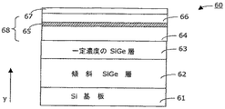
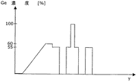
さらに別の実施形態を図6及び図7に示す。デバイス60は、図5に図示したものと類似である。デバイス60は、Si基板61を含んでおり、このSi基板61の上に、仮想SiGe基板が形成されている。仮想基板は、傾斜SiGe層62と、濃度X=0.6の一定のGe濃度のバッファ層63とを含んでいる。各層の厚さの比率は、正確ではない。活性領域68は、仮想基板の上に形成されている。活性領域68は、クラッド層64を含んでおり、このクラッド層64のGe濃度は、バッファ層63のGe濃度よりも低く、X=0.55である。クラッド層64は、変調ドーピングを含んでいる。Geチャンネル65は、変調ドープクラッド層64の上に形成されている。このGeチャンネル65は、別の変調ドープクラッド層66及びSiキャップ層67に覆われている。低いGe濃度の2つのクラッド層54、56は、活性領域58の歪みの補償を提供している。Ge濃度のプロフィルを図7に示す。変調ドープ層64及び66は、それぞれ1つのドーピングスパイクを含んでいる。
Yet another embodiment is shown in FIGS.
本発明の半導体構造体の形成方法は、以下の工程を含んでいる。
以下の条件の、高密度の低エネルギープラズマ強化化学蒸着法(LEPECVD)を用いて、Si基板上に仮想基板を形成する工程。仮想基板は、傾斜Si1−xGex層で0≦X≦Xfの層と、Ge濃度が一定のSi1−xGex層と、を含んでいる。この工程は、
i.成長速度が2nm/s以上
ii.基板温度が400℃〜850℃
iii.成長チャンバのガス導入口における全反応ガス流が5sccm〜200sccm
の条件で行われる。
以下の条件の、低密度の低エネルギープラズマ強化化学蒸着法(LEPECVD)を用いて、仮想基板上に活性領域を形成する工程。活性領域は、Geチャンネルと、少なくとも1つの変調ドープ層を含んでいる。この工程は、
i.成長チャンバ内に水素(H2)を導入して、界面活性剤として機能させる
ii.基板温度を400℃〜500℃に保持する
iii.成長チャンバ内にドーパントガスをパルス状に導入し、変調ドープ層を形成する
の条件を含んでいる。
The method for forming a semiconductor structure of the present invention includes the following steps.
A step of forming a virtual substrate on a Si substrate using a high density low energy plasma enhanced chemical vapor deposition (LEPECVD) under the following conditions. The virtual substrate includes an inclined Si 1-x Ge x layer, a layer of 0 ≦ X ≦ X f , and a Si 1-x Ge x layer having a constant Ge concentration. This process
i. Growth rate is 2nm / s or more
ii. Substrate temperature is 400 ° C to 850 ° C
iii. The total reactive gas flow at the gas inlet of the growth chamber is 5 sccm to 200 sccm
It is performed under the conditions of
A step of forming an active region on a virtual substrate using a low density low energy plasma enhanced chemical vapor deposition (LEPECVD) under the following conditions. The active region includes a Ge channel and at least one modulation doped layer. This process
i. Hydrogen (H 2 ) is introduced into the growth chamber to function as a surfactant.
ii. The substrate temperature is maintained at 400 ° C. to 500 ° C.
iii. The conditions include introducing a dopant gas into the growth chamber in a pulsed manner to form a modulation doped layer.
本発明の方法は、さまざまに変更することができる。 The method of the present invention can be variously modified.
本発明によれば、特別な成長システム80は、本発明の方法を自動処理に使用して実現できる。一例を図8に示す。この成長システム80は、ガス導入口及び他の部品を備えた成長チャンバ23を含んでおり、図2に示したものに類似している。この成長システム80は、少なくとも2つの工程を含む低エネルギープラズマ強化化学蒸着法(LEPECVD)を行うために装備されている。第1の処理工程中のシステムパラメータは、基板温度が400℃〜850℃、ガス導入口での全反応ガス流量が5sccm〜200sccmであり、成長速度が2nm/s以上になるになるように調整される。第2の処理工程中のシステムパラメータは、基板温度を400℃〜500℃に保持するように調整される。さらに、水素(H2)を成長チャンバに導入し、且つドーパントガスを成長チャンバにパルス状に導入して、少なくとも1つの層に変調ドーピングできるようにされている。
According to the present invention, a
図8に概略的に示すように、本発明に係る成長システム80は、処理制御ユニット81、好ましくは適当なソフトウェアモジュール82及び83を備えたコンピュータを含んでおり、システムパラメータを制御することができる。
As schematically shown in FIG. 8, the
本発明の方法によれば、RMF表面粗さ5nm以下のSiGe層を形成することができる。 According to the method of the present invention, a SiGe layer having an RMF surface roughness of 5 nm or less can be formed.
本発明の概念は、トランジスタ、センサ、分光法、量子コンピュータ、及びその他のデバイス/システムに用いるのに非常に適している。 The inventive concept is well suited for use in transistors, sensors, spectroscopy, quantum computers, and other devices / systems.
Claims (19)
以下の条件による高密度の低エネルギープラズマ強化化学蒸着法(LEPECVD)を用いて、シリコン基板(11、51、61)上に、傾斜Si1−xGex層(12、52、62)とそれに続いてGe濃度一定のSi1−xGex層(13、53、63)とを含む仮想基板を形成する工程であって、高密度のLEPECVDの条件が、
i.成長速度が2nm/s以上、
ii.基板温度が400℃〜850℃、及び
iii.ガス導入口での全反応ガス流量が5sccm〜200sccm、の工程と、
以下の条件による低密度の低エネルギープラズマ強化化学蒸着法(LEPECVD)を用いて、上記仮想基板上に、Geチャンネル(55、65)と変調ドープ層(56、64、67)とを含む活性領域(14、58、68)を形成する工程であって、低密度のLEPECVDの条件が、
i.成長チャンバ(23)に水素(H2)を導入して、界面活性剤として機能させること、
ii.基板温度を400℃〜500℃に保持すること、及び
iii.成長チャンバ(23)にドーパントガスをパルス状に導入し、上記変調ドープ層(56、64、67)を形成すること、である工程と、
を含んでいる半導体ヘテロ構造体の製造方法。 A method of manufacturing a semiconductor heterostructure in a growth chamber (23) having gas inlets (26, 30), wherein the manufacturing method comprises
Using a high density low energy plasma enhanced chemical vapor deposition (LEPECVD) under the following conditions, a graded Si 1-x Ge x layer (12, 52, 62) and a silicon substrate (11, 51, 61) Subsequently, a process of forming a virtual substrate including a Si 1-x Ge x layer (13, 53, 63) having a constant Ge concentration, wherein the conditions for high-density LEPECVD are:
i. Growth rate is 2 nm / s or more,
ii. The substrate temperature is 400 ° C. to 850 ° C., and
iii. A process in which the total reaction gas flow rate at the gas inlet is 5 sccm to 200 sccm;
An active region including a Ge channel (55, 65) and a modulation doped layer (56, 64, 67) on the virtual substrate using a low density low energy plasma enhanced chemical vapor deposition (LEPECVD) under the following conditions: (14, 58, 68), wherein the low density LEPECVD conditions are:
i. Introducing hydrogen (H 2 ) into the growth chamber (23) to function as a surfactant;
ii. Maintaining the substrate temperature between 400 ° C. and 500 ° C .; and
iii. Introducing a dopant gas into the growth chamber (23) in a pulsed manner to form the modulation doped layer (56, 64, 67);
A method for manufacturing a semiconductor heterostructure including:
シリコン基板(11、51、61)と、
傾斜Si1−xGex層(12、52、62)と、
Ge濃度一定のSi1−xGexバッファ層(13、53、63)と、
上記バッファ層(13、53、63)上に位置している活性領域(14、58、68)と、
4.2Kにおいて70000〜87000cm2/Vsのホール移動度を有するGeチャンネル(55、65)と、を含んでおり、
上記活性領域(14、58、68)が、少なくとも1つの変調ドープ層(56、64、67)を含む半導体デバイス。 A heterostructure semiconductor device comprising:
A silicon substrate (11, 51, 61);
Graded Si 1-x Ge x layers (12, 52, 62);
A Si 1-x Ge x buffer layer (13, 53, 63) having a constant Ge concentration;
Active regions (14, 58, 68) located on the buffer layers (13, 53, 63);
And a Ge channel (55, 65) having a hole mobility of 70000-87000 cm 2 / Vs at 4.2K,
A semiconductor device wherein the active region (14, 58, 68) comprises at least one modulation doped layer (56, 64, 67).
成長システム(80)は、少なくとも2つの工程を含む低密度の低エネルギープラズマ強化化学蒸着法(LEPECVD)を行うために装備されており、これにより
第1の処理工程中のシステムパラメータが、基板温度を400℃〜850℃、ガス導入口での全反応ガス流量を5sccm〜200sccmにして、成長速度を2nm/s以上にするように調整され、
第2の処理工程中のシステムパラメータが、基板温度を400℃〜500℃に保持するように調整され、水素(H2)を成長チャンバ(23)に導入し、且つドーパントガスを成長チャンバ(23)にパルス状に導入して、少なくとも1つの層に変調ドーピングできる、成長システム。 A growth system (80) comprising a growth chamber (23) with gas inlets (26, 30),
The growth system (80) is equipped to perform a low density, low energy plasma enhanced chemical vapor deposition (LEPECVD) process comprising at least two steps, whereby the system parameters during the first processing step are determined by the substrate temperature. Is adjusted to 400 ° C. to 850 ° C., the total reaction gas flow rate at the gas inlet is 5 sccm to 200 sccm, and the growth rate is 2 nm / s or more,
System parameters during the second processing step are adjusted to maintain the substrate temperature between 400 ° C. and 500 ° C., hydrogen (H 2 ) is introduced into the growth chamber (23), and dopant gas is introduced into the growth chamber (23 A growth system which can be introduced in a pulsed manner into the at least one layer.
The processing control unit (81), the growth system of claim 13 capable of controlling the introduction into the growth chamber of the SiH 4 and GeH 4 (23).
Applications Claiming Priority (2)
| Application Number | Priority Date | Filing Date | Title |
|---|---|---|---|
| EP01127834A EP1315199A1 (en) | 2001-11-22 | 2001-11-22 | Formation of high-mobility silicon-germanium structures by low-energy plasma enhanced chemical vapor deposition |
| PCT/EP2002/009922 WO2003044839A2 (en) | 2001-11-22 | 2002-09-05 | Formation of high-mobility silicon-germanium structures by low-energy plasma enhanced chemical vapor deposition |
Publications (2)
| Publication Number | Publication Date |
|---|---|
| JP2005510081A true JP2005510081A (en) | 2005-04-14 |
| JP2005510081A5 JP2005510081A5 (en) | 2006-01-05 |
Family
ID=8179316
Family Applications (1)
| Application Number | Title | Priority Date | Filing Date |
|---|---|---|---|
| JP2003546385A Pending JP2005510081A (en) | 2001-11-22 | 2002-09-05 | Fabrication method of high mobility silicon germanium structure by low energy plasma enhanced chemical vapor deposition |
Country Status (6)
| Country | Link |
|---|---|
| US (1) | US7115895B2 (en) |
| EP (1) | EP1315199A1 (en) |
| JP (1) | JP2005510081A (en) |
| CN (1) | CN100345254C (en) |
| AU (1) | AU2002335310A1 (en) |
| WO (1) | WO2003044839A2 (en) |
Cited By (2)
| Publication number | Priority date | Publication date | Assignee | Title |
|---|---|---|---|---|
| JP2010267969A (en) * | 2009-05-13 | 2010-11-25 | Siltronic Ag | Method for producing wafer including silicon single crystal substrate having front side and back side and layer of sige deposited on the front side |
| KR20140147250A (en) * | 2013-06-19 | 2014-12-30 | 엘지이노텍 주식회사 | Semiconductor substrate, light emitting device, and Electronic device |
Families Citing this family (14)
| Publication number | Priority date | Publication date | Assignee | Title |
|---|---|---|---|---|
| US6855436B2 (en) * | 2003-05-30 | 2005-02-15 | International Business Machines Corporation | Formation of silicon-germanium-on-insulator (SGOI) by an integral high temperature SIMOX-Ge interdiffusion anneal |
| AU2003223991A1 (en) * | 2003-03-26 | 2004-10-18 | Eidgenoessische Technische Hochschule Zuerich | Formation of thin semiconductor layers by low-energy plasma enhanced chemical vapor deposition and semiconductor heterostructure devices |
| EP1513233B1 (en) * | 2003-09-05 | 2008-10-29 | Epispeed S.A. | InGaAs/GaAs lasers on Silicon produced by LEPECVD and MOCVD |
| EP1745165B1 (en) | 2004-04-30 | 2011-03-30 | Dichroic cell s.r.l. | Method for producing virtual ge substrates for iii/v-integration on si(001) |
| JP2007250903A (en) * | 2006-03-16 | 2007-09-27 | Matsushita Electric Ind Co Ltd | Heterojunction bipolar transistor and manufacturing method therefor |
| EP2049939A1 (en) * | 2006-08-11 | 2009-04-22 | Paul Scherrer Institut | Light modulators comprising si-ge quantum well layers |
| JP5308336B2 (en) | 2006-08-25 | 2013-10-09 | ブレイン アンド サイエンス エルエルシー | A system to detect a specific cognitive emotional state of a subject |
| FR2914783A1 (en) * | 2007-04-03 | 2008-10-10 | St Microelectronics Sa | METHOD FOR MANUFACTURING CONCENTRATING GRADIENT DEVICE AND CORRESPONDING DEVICE. |
| US20110017127A1 (en) * | 2007-08-17 | 2011-01-27 | Epispeed Sa | Apparatus and method for producing epitaxial layers |
| US8237126B2 (en) * | 2007-08-17 | 2012-08-07 | Csem Centre Suisse D'electronique Et De Mictrotechnique Sa | X-ray imaging device and method for the manufacturing thereof |
| TWI562195B (en) | 2010-04-27 | 2016-12-11 | Pilegrowth Tech S R L | Dislocation and stress management by mask-less processes using substrate patterning and methods for device fabrication |
| CN103165420B (en) * | 2011-12-14 | 2015-11-18 | 中国科学院上海微系统与信息技术研究所 | The method that superlattice prepare strain Si is embedded in a kind of SiGe |
| CN105632927B (en) * | 2014-10-30 | 2018-09-07 | 中芯国际集成电路制造(上海)有限公司 | The forming method of PMOS transistor |
| KR102465536B1 (en) * | 2016-06-08 | 2022-11-14 | 삼성전자주식회사 | Method of manufacturing semiconductor devices |
Family Cites Families (4)
| Publication number | Priority date | Publication date | Assignee | Title |
|---|---|---|---|---|
| EP0380077A3 (en) * | 1989-01-25 | 1990-09-12 | Hitachi, Ltd. | Transistor provided with strained germanium layer |
| US5241197A (en) * | 1989-01-25 | 1993-08-31 | Hitachi, Ltd. | Transistor provided with strained germanium layer |
| US5442205A (en) * | 1991-04-24 | 1995-08-15 | At&T Corp. | Semiconductor heterostructure devices with strained semiconductor layers |
| ATE394794T1 (en) * | 1999-03-12 | 2008-05-15 | Ibm | HIGH VELOCITY GE CHANNEL HETEROSTRUCTURE FOR FIELD EFFECT ARRANGEMENTS |
-
2001
- 2001-11-22 EP EP01127834A patent/EP1315199A1/en not_active Withdrawn
-
2002
- 2002-09-05 JP JP2003546385A patent/JP2005510081A/en active Pending
- 2002-09-05 CN CNB028273095A patent/CN100345254C/en not_active Expired - Fee Related
- 2002-09-05 WO PCT/EP2002/009922 patent/WO2003044839A2/en active Application Filing
- 2002-09-05 AU AU2002335310A patent/AU2002335310A1/en not_active Abandoned
- 2002-09-05 US US10/496,245 patent/US7115895B2/en not_active Expired - Fee Related
Cited By (3)
| Publication number | Priority date | Publication date | Assignee | Title |
|---|---|---|---|---|
| JP2010267969A (en) * | 2009-05-13 | 2010-11-25 | Siltronic Ag | Method for producing wafer including silicon single crystal substrate having front side and back side and layer of sige deposited on the front side |
| KR20140147250A (en) * | 2013-06-19 | 2014-12-30 | 엘지이노텍 주식회사 | Semiconductor substrate, light emitting device, and Electronic device |
| KR102142707B1 (en) * | 2013-06-19 | 2020-08-07 | 엘지이노텍 주식회사 | Semiconductor substrate, light emitting device, and Electronic device |
Also Published As
| Publication number | Publication date |
|---|---|
| AU2002335310A8 (en) | 2003-06-10 |
| WO2003044839A2 (en) | 2003-05-30 |
| AU2002335310A1 (en) | 2003-06-10 |
| WO2003044839A3 (en) | 2003-10-30 |
| EP1315199A1 (en) | 2003-05-28 |
| US7115895B2 (en) | 2006-10-03 |
| CN1615540A (en) | 2005-05-11 |
| US20050116226A1 (en) | 2005-06-02 |
| CN100345254C (en) | 2007-10-24 |
Similar Documents
| Publication | Publication Date | Title |
|---|---|---|
| US9934964B2 (en) | Semiconductor heterostructures having reduced dislocation pile-ups and related methods | |
| US6593625B2 (en) | Relaxed SiGe layers on Si or silicon-on-insulator substrates by ion implantation and thermal annealing | |
| US7060632B2 (en) | Methods for fabricating strained layers on semiconductor substrates | |
| TWI382456B (en) | Epitaxial growth of relaxed silicon germanium layers | |
| US20040092085A1 (en) | Semiconductor crystal film and method for preparation thereof | |
| JP5065676B2 (en) | Method and layer structure for producing a strained layer on a substrate | |
| JP2005510081A (en) | Fabrication method of high mobility silicon germanium structure by low energy plasma enhanced chemical vapor deposition | |
| Fitzgerald | GeSi/Si Nanostructures | |
| Seal et al. | Chemical vapor deposition growth and characterization of undoped and doped Ge and Ge 1− x C x quantum dots on Si | |
| US7678645B2 (en) | Formation of thin semiconductor layers by low-energy plasma enhanced chemical vapor deposition and semiconductor heterostructure devices | |
| Rosenblad et al. | Low Energy Plasma Enhanced Chemical Vapour Deposition-Plasma Enhanced Deposition of Epitaxial Si and Sige | |
| Rosenblad et al. | Virtual substrates for the n-and p-type Si-MODFET grown at very high rates | |
| Grimm et al. | Annealing experiments on supercritical Si1–xGex layers grown by RPCVD | |
| Hammond | The structural and electrical characterisation of SiGe heterostructures deposited on strain relaxed virtual substrates | |
| BLOWER | SPEC. GAS SOURCE FURNACE |
Legal Events
| Date | Code | Title | Description |
|---|---|---|---|
| A521 | Written amendment |
Free format text: JAPANESE INTERMEDIATE CODE: A523 Effective date: 20050816 |
|
| A621 | Written request for application examination |
Free format text: JAPANESE INTERMEDIATE CODE: A621 Effective date: 20050816 |
|
| RD03 | Notification of appointment of power of attorney |
Free format text: JAPANESE INTERMEDIATE CODE: A7423 Effective date: 20070730 |
|
| A521 | Written amendment |
Free format text: JAPANESE INTERMEDIATE CODE: A821 Effective date: 20070730 |
|
| A977 | Report on retrieval |
Free format text: JAPANESE INTERMEDIATE CODE: A971007 Effective date: 20081030 |
|
| A131 | Notification of reasons for refusal |
Free format text: JAPANESE INTERMEDIATE CODE: A131 Effective date: 20081111 |
|
| A521 | Written amendment |
Free format text: JAPANESE INTERMEDIATE CODE: A523 Effective date: 20090210 |
|
| A02 | Decision of refusal |
Free format text: JAPANESE INTERMEDIATE CODE: A02 Effective date: 20090602 |