JP2005509899A - Optical device with reflective and transmissive modes for display - Google Patents
Optical device with reflective and transmissive modes for display Download PDFInfo
- Publication number
- JP2005509899A JP2005509899A JP2003544520A JP2003544520A JP2005509899A JP 2005509899 A JP2005509899 A JP 2005509899A JP 2003544520 A JP2003544520 A JP 2003544520A JP 2003544520 A JP2003544520 A JP 2003544520A JP 2005509899 A JP2005509899 A JP 2005509899A
- Authority
- JP
- Japan
- Prior art keywords
- light
- display device
- layer
- optical cavity
- reflective polarizer
- Prior art date
- Legal status (The legal status is an assumption and is not a legal conclusion. Google has not performed a legal analysis and makes no representation as to the accuracy of the status listed.)
- Withdrawn
Links
- 230000003287 optical effect Effects 0.000 title claims abstract description 72
- 230000010287 polarization Effects 0.000 claims abstract description 77
- 230000028161 membrane depolarization Effects 0.000 claims abstract description 33
- 230000003098 cholesteric effect Effects 0.000 claims abstract description 17
- 230000005540 biological transmission Effects 0.000 claims abstract description 12
- 230000010363 phase shift Effects 0.000 claims abstract description 8
- 238000009792 diffusion process Methods 0.000 claims description 23
- 239000011248 coating agent Substances 0.000 claims description 10
- 238000000576 coating method Methods 0.000 claims description 10
- 238000005286 illumination Methods 0.000 claims description 10
- 229910052751 metal Inorganic materials 0.000 claims description 8
- 239000002184 metal Substances 0.000 claims description 8
- 230000009977 dual effect Effects 0.000 abstract description 4
- 239000010410 layer Substances 0.000 description 88
- 230000000694 effects Effects 0.000 description 12
- 229920000642 polymer Polymers 0.000 description 9
- 238000012937 correction Methods 0.000 description 4
- 239000003085 diluting agent Substances 0.000 description 4
- 238000000034 method Methods 0.000 description 4
- 230000002093 peripheral effect Effects 0.000 description 4
- 238000002310 reflectometry Methods 0.000 description 4
- BQCADISMDOOEFD-UHFFFAOYSA-N Silver Chemical compound [Ag] BQCADISMDOOEFD-UHFFFAOYSA-N 0.000 description 3
- 239000012790 adhesive layer Substances 0.000 description 3
- 229910052782 aluminium Inorganic materials 0.000 description 3
- XAGFODPZIPBFFR-UHFFFAOYSA-N aluminium Chemical compound [Al] XAGFODPZIPBFFR-UHFFFAOYSA-N 0.000 description 3
- 230000005684 electric field Effects 0.000 description 3
- 239000002245 particle Substances 0.000 description 3
- 238000004064 recycling Methods 0.000 description 3
- 229910052709 silver Inorganic materials 0.000 description 3
- 239000004332 silver Substances 0.000 description 3
- 239000000758 substrate Substances 0.000 description 3
- 239000000853 adhesive Substances 0.000 description 2
- 230000001070 adhesive effect Effects 0.000 description 2
- 239000006185 dispersion Substances 0.000 description 2
- 238000003709 image segmentation Methods 0.000 description 2
- 238000007689 inspection Methods 0.000 description 2
- 239000000463 material Substances 0.000 description 2
- 150000002739 metals Chemical class 0.000 description 2
- 238000012986 modification Methods 0.000 description 2
- 230000004048 modification Effects 0.000 description 2
- 229920000139 polyethylene terephthalate Polymers 0.000 description 2
- 239000005020 polyethylene terephthalate Substances 0.000 description 2
- -1 silver and aluminum Chemical class 0.000 description 2
- 239000011800 void material Substances 0.000 description 2
- 229920002799 BoPET Polymers 0.000 description 1
- 229910010413 TiO 2 Inorganic materials 0.000 description 1
- 238000010521 absorption reaction Methods 0.000 description 1
- 230000002051 biphasic effect Effects 0.000 description 1
- 230000000903 blocking effect Effects 0.000 description 1
- 230000008859 change Effects 0.000 description 1
- 238000001816 cooling Methods 0.000 description 1
- 230000003247 decreasing effect Effects 0.000 description 1
- 238000013461 design Methods 0.000 description 1
- 230000007613 environmental effect Effects 0.000 description 1
- 239000012456 homogeneous solution Substances 0.000 description 1
- 238000003384 imaging method Methods 0.000 description 1
- 238000012423 maintenance Methods 0.000 description 1
- 238000004519 manufacturing process Methods 0.000 description 1
- 238000005259 measurement Methods 0.000 description 1
- 230000036314 physical performance Effects 0.000 description 1
- 229920006254 polymer film Polymers 0.000 description 1
- 230000008569 process Effects 0.000 description 1
- 239000011241 protective layer Substances 0.000 description 1
- 238000010791 quenching Methods 0.000 description 1
- 230000000171 quenching effect Effects 0.000 description 1
- 230000009467 reduction Effects 0.000 description 1
- 229920006126 semicrystalline polymer Polymers 0.000 description 1
- 238000000926 separation method Methods 0.000 description 1
- 239000002904 solvent Substances 0.000 description 1
- 125000006850 spacer group Chemical group 0.000 description 1
- 238000002145 thermally induced phase separation Methods 0.000 description 1
Images


Classifications
-
- G—PHYSICS
- G02—OPTICS
- G02F—OPTICAL DEVICES OR ARRANGEMENTS FOR THE CONTROL OF LIGHT BY MODIFICATION OF THE OPTICAL PROPERTIES OF THE MEDIA OF THE ELEMENTS INVOLVED THEREIN; NON-LINEAR OPTICS; FREQUENCY-CHANGING OF LIGHT; OPTICAL LOGIC ELEMENTS; OPTICAL ANALOGUE/DIGITAL CONVERTERS
- G02F1/00—Devices or arrangements for the control of the intensity, colour, phase, polarisation or direction of light arriving from an independent light source, e.g. switching, gating or modulating; Non-linear optics
- G02F1/01—Devices or arrangements for the control of the intensity, colour, phase, polarisation or direction of light arriving from an independent light source, e.g. switching, gating or modulating; Non-linear optics for the control of the intensity, phase, polarisation or colour
- G02F1/13—Devices or arrangements for the control of the intensity, colour, phase, polarisation or direction of light arriving from an independent light source, e.g. switching, gating or modulating; Non-linear optics for the control of the intensity, phase, polarisation or colour based on liquid crystals, e.g. single liquid crystal display cells
- G02F1/133—Constructional arrangements; Operation of liquid crystal cells; Circuit arrangements
- G02F1/1333—Constructional arrangements; Manufacturing methods
- G02F1/1335—Structural association of cells with optical devices, e.g. polarisers or reflectors
- G02F1/1336—Illuminating devices
- G02F1/13362—Illuminating devices providing polarized light, e.g. by converting a polarisation component into another one
-
- G—PHYSICS
- G02—OPTICS
- G02F—OPTICAL DEVICES OR ARRANGEMENTS FOR THE CONTROL OF LIGHT BY MODIFICATION OF THE OPTICAL PROPERTIES OF THE MEDIA OF THE ELEMENTS INVOLVED THEREIN; NON-LINEAR OPTICS; FREQUENCY-CHANGING OF LIGHT; OPTICAL LOGIC ELEMENTS; OPTICAL ANALOGUE/DIGITAL CONVERTERS
- G02F1/00—Devices or arrangements for the control of the intensity, colour, phase, polarisation or direction of light arriving from an independent light source, e.g. switching, gating or modulating; Non-linear optics
- G02F1/01—Devices or arrangements for the control of the intensity, colour, phase, polarisation or direction of light arriving from an independent light source, e.g. switching, gating or modulating; Non-linear optics for the control of the intensity, phase, polarisation or colour
- G02F1/13—Devices or arrangements for the control of the intensity, colour, phase, polarisation or direction of light arriving from an independent light source, e.g. switching, gating or modulating; Non-linear optics for the control of the intensity, phase, polarisation or colour based on liquid crystals, e.g. single liquid crystal display cells
- G02F1/133—Constructional arrangements; Operation of liquid crystal cells; Circuit arrangements
- G02F1/1333—Constructional arrangements; Manufacturing methods
- G02F1/1335—Structural association of cells with optical devices, e.g. polarisers or reflectors
- G02F1/133528—Polarisers
- G02F1/133536—Reflective polarizers
-
- G—PHYSICS
- G02—OPTICS
- G02F—OPTICAL DEVICES OR ARRANGEMENTS FOR THE CONTROL OF LIGHT BY MODIFICATION OF THE OPTICAL PROPERTIES OF THE MEDIA OF THE ELEMENTS INVOLVED THEREIN; NON-LINEAR OPTICS; FREQUENCY-CHANGING OF LIGHT; OPTICAL LOGIC ELEMENTS; OPTICAL ANALOGUE/DIGITAL CONVERTERS
- G02F2201/00—Constructional arrangements not provided for in groups G02F1/00 - G02F7/00
- G02F2201/34—Constructional arrangements not provided for in groups G02F1/00 - G02F7/00 reflector
- G02F2201/343—Constructional arrangements not provided for in groups G02F1/00 - G02F7/00 reflector cholesteric liquid crystal reflector
-
- G—PHYSICS
- G02—OPTICS
- G02F—OPTICAL DEVICES OR ARRANGEMENTS FOR THE CONTROL OF LIGHT BY MODIFICATION OF THE OPTICAL PROPERTIES OF THE MEDIA OF THE ELEMENTS INVOLVED THEREIN; NON-LINEAR OPTICS; FREQUENCY-CHANGING OF LIGHT; OPTICAL LOGIC ELEMENTS; OPTICAL ANALOGUE/DIGITAL CONVERTERS
- G02F2203/00—Function characteristic
- G02F2203/09—Function characteristic transflective
Landscapes
- Physics & Mathematics (AREA)
- Nonlinear Science (AREA)
- Mathematical Physics (AREA)
- Chemical & Material Sciences (AREA)
- Crystallography & Structural Chemistry (AREA)
- General Physics & Mathematics (AREA)
- Optics & Photonics (AREA)
- Liquid Crystal (AREA)
- Devices For Indicating Variable Information By Combining Individual Elements (AREA)
- Polarising Elements (AREA)
- Optical Elements Other Than Lenses (AREA)
Abstract
ディスプレイ装置(100;200;400;500;1400)は、周辺光(110;210;510)のみを用いた反射モードおよび光源(105;205;505;1405)を用いた透過モードで、情報を表示することができることが示されている。一実施形態において、ディスプレイ装置(100;1400)は、光変調層(102;1402)と等方性光キャビティ(105;106;1405;1406)との間に配置される反射偏光子(104;1408)を具備している。光キャビティ(105;106;1405;1406)は、第1の偏光を有する入射光を反射する。反射偏光子(104;1408)は、少なくとも1つの偏光に関して、第1の程度の脱偏光より大きい第2の程度の脱偏光を有する光を反射する。ディスプレイ装置(200;1400)の別の実施形態において、微細構造フィルム(204;1404)は少なくとも傾斜面(211、212;1411、1412)を有する鋸歯構成(207;1407)を備えている場合に、微細構造フィルム(204;1404)は、光キャビティ(205、206;1405、1406)の上であり、光変調システム(201、202、203、208、1401、1402、1403、1415)の下に具備されている。デュアルモードディスプレイ装置(500)の別の実施形態において、ディスプレイ(500)は、光変調層(502)と光キャビティ(505、506)との間に配置されるコレステリック反射偏光子(504)を具備し、光キャビティ(505、506)は、反射時に偏光位相シフトを生じる。 The display device (100; 200; 400; 500; 1400) displays information in reflection mode using only ambient light (110; 210; 510) and transmission mode using a light source (105; 205; 505; 1405). It is shown that it can be displayed. In one embodiment, the display device (100; 1400) includes a reflective polarizer (104; 1408) disposed between the light modulating layer (102; 1402) and the isotropic optical cavity (105; 106; 1405; 1406). It has. The optical cavities (105; 106; 1405; 1406) reflect incident light having a first polarization. The reflective polarizer (104; 1408) reflects light having a second degree of depolarization greater than the first degree of depolarization for at least one polarization. In another embodiment of the display device (200; 1400), the microstructured film (204; 1404) comprises a sawtooth configuration (207; 1407) having at least inclined surfaces (211; 212; 1411; 1412). The microstructured film (204; 1404) is above the light cavity (205, 206; 1405, 1406) and below the light modulation system (201, 202, 203, 208, 1401, 1402, 1403, 1415). It is equipped. In another embodiment of the dual mode display device (500), the display (500) comprises a cholesteric reflective polarizer (504) disposed between the light modulation layer (502) and the light cavity (505, 506). The optical cavities (505, 506) cause a polarization phase shift when reflected.
Description
本発明は一般に、反射モードおよび透過モードの両方で情報を表示することができる光学デバイスに関する。 The present invention relates generally to optical devices capable of displaying information in both reflective and transmissive modes.
携帯電話などのハンドヘルド型電子デバイスの多くは、像形成のために周辺照明またはバックライトの両方を用いて動作することができるディスプレイを具備している。このようなディスプレイは、透過モードおよび反射モードのいずれでも動作すると言われ、一般に半透過型(transflective)ディスプレイと呼ばれている。これらのディスプレイは、周辺光が利用可能であるときには周辺光を用い、必要である場合または利用者によって選択された場合にのみバックライトを用いる。バックライトへの依存性を小さくすることにより、電力消費を削減し、バッテリ寿命をより長くすることができる。 Many handheld electronic devices, such as cell phones, include a display that can be operated with both ambient lighting or backlighting for imaging. Such a display is said to operate in both transmissive and reflective modes and is commonly referred to as a transflective display. These displays use ambient light when ambient light is available and use a backlight only when necessary or selected by the user. By reducing the dependency on the backlight, it is possible to reduce power consumption and extend battery life.
このような半透過型ディスプレイは、部分的またはパターン形成された金属ミラー、または適切な反射粒子を装着した透明ポリマーであってもよい半透過層を具備している。この半透過層は、反射モードでディスプレイを形成する際に用いるための周辺光を反射し、透過モードでディスプレイを形成する際に用いるためのバックライトからの光を透過するように設計される。半透過層は、2つの動作モード間の強度バランスを図っている。半透過体の透過特性がバックライト中または透過作動中の照明を改善するために増大する場合には、半透過層によって反射される周辺光が少ないため、反射モードまたは周辺光モード動作中にディスプレイの明るさが減少している。逆に言えば、半透過体の反射率を改善することにより、周辺光の明るさを増大させるが、バックライティング動作中の明るさを犠牲にする。 Such a transflective display comprises a transflective layer, which may be a partially or patterned metal mirror, or a transparent polymer fitted with suitable reflective particles. This transflective layer is designed to reflect ambient light for use in forming the display in the reflective mode and to transmit light from the backlight for use in forming the display in the transmissive mode. The transflective layer balances the intensity between the two operation modes. If the transflective properties of the transflector increase to improve illumination in backlight or transmissive operation, less ambient light is reflected by the transflective layer, so the display during reflective or ambient light mode operation The brightness has decreased. Conversely, the brightness of the ambient light is increased by improving the reflectivity of the transflector, but at the expense of the brightness during the backlighting operation.
一実施形態において、ディスプレイ装置は、周辺光のみを用いた反射モードおよび光源を用いた透過モードで、情報を表示することができる。ディスプレイ装置は、反射偏光子と、反射体を有する等方性光キャビティと、を具備している。光キャビティは、入射光の第1の程度の脱偏光を伴なって入射光を反射する。光変調層と光キャビティとの間に配置される反射偏光子は、第1の偏光を有する入射光の成分を透過し、第2の偏光を有する入射光の成分を反射するようになされる。反射偏光子は、第1の程度の脱偏光より大きい第2の程度の脱偏光をもって第2の偏光の光を反射し、第1の偏光の一部の光を形成する。ディスプレイ装置は、半透過層を具備しないことが好ましい。一実施形態において、光キャビティは、反射において偏光状態を実質的に維持する。 In one embodiment, the display device can display information in a reflective mode using only ambient light and a transmissive mode using a light source. The display device includes a reflective polarizer and an isotropic optical cavity having a reflector. The optical cavity reflects incident light with a first degree of depolarization of the incident light. The reflective polarizer disposed between the light modulation layer and the optical cavity transmits the incident light component having the first polarization and reflects the incident light component having the second polarization. The reflective polarizer reflects light of the second polarization with a second degree of depolarization greater than the first degree of depolarization to form part of the first polarization. The display device preferably does not include a semi-transmissive layer. In one embodiment, the optical cavity substantially maintains the polarization state in reflection.
本発明の第2の実施形態において、ディスプレイ装置は、光キャビティの上であり、光変調システムの下に位置する第1の微細構造フィルムを具備している。第1の微細構造フィルムは鋸歯構成を備え、鋸歯構成のそれぞれが傾斜面を備えている。周辺光が第1の微細構造フィルムに当たる場合には、周辺光の入射エネルギーにおける第1の部分が第1の角度方向に屈折し、周辺光の入射エネルギーにおける第2の部分が第1の角度方向とは異なる第2の角度方向に屈折する。このディスプレイは、周辺光のみを用いてまたは光源からの光のみを用いて作動することができる。ディスプレイ装置は、半透過層を具備していないことが好ましい。鋸歯構成は、プリズムまたは角錐形状を備えていてもよい。ディスプレイ装置の第3の実施形態において、第2の微細構造フィルムがディスプレイ装置に具備される。 In a second embodiment of the invention, the display device comprises a first microstructured film located above the optical cavity and below the light modulation system. The first microstructured film has a sawtooth configuration, each of the sawtooth configurations having an inclined surface. When the ambient light strikes the first microstructured film, the first portion of the incident light of the ambient light is refracted in the first angular direction, and the second portion of the incident light of the ambient light is the first angular direction. Refracts in a second angular direction different from. The display can be operated using only ambient light or only light from the light source. The display device preferably does not include a transflective layer. The sawtooth configuration may comprise a prism or pyramid shape. In a third embodiment of the display device, a second microstructured film is provided in the display device.
本発明の第4の実施形態において、ディスプレイ装置は、光変調システムと、光変調層に光を選択的に提供するようになされた光キャビティと、コレステリック反射偏光子と、を具備している。光キャビティは、反射時に偏光位相シフトを生じるように構成される。コレステリック反射偏光子は、光変調層と光キャビティとの間に配置され、第1の偏光を有する入射光の成分を透過し、第2の偏光を有する入射光の成分を反射するようになされる。このディスプレイはまた、周辺光のみを用いてまたは光源からの光のみを用いて作動することができる。ディスプレイ装置は、半透過層を具備していないことが好ましい。 In a fourth embodiment of the present invention, a display device comprises a light modulation system, a light cavity adapted to selectively provide light to a light modulation layer, and a cholesteric reflective polarizer. The optical cavity is configured to produce a polarization phase shift upon reflection. The cholesteric reflective polarizer is disposed between the light modulation layer and the optical cavity, and is configured to transmit a component of incident light having a first polarization and reflect a component of incident light having a second polarization. . The display can also operate using only ambient light or only light from a light source. The display device preferably does not include a transflective layer.
本発明は、添付図面と共に本発明のさまざまな実施形態に関する以下の詳細な説明を考慮すればさらに完全に理解されると思われる。 The present invention will be more fully understood in view of the following detailed description of various embodiments of the invention in conjunction with the accompanying drawings.
本発明はさまざまな修正形態および代替形態に基づいて吟味されるが、その仕様は図面によって示され、詳細に説明される。しかし、記載された特定の実施形態に本発明を限定するわけではないことを理解されたい。逆に言えば、添付特許請求の範囲によって定義されるように、本発明の精神および範囲を逸脱することなく、すべての修正物、等価物および代替物を網羅するものとする。 The invention will be examined on the basis of various modifications and alternatives, the specification of which is illustrated by the drawings and explained in detail. However, it should be understood that the invention is not limited to the specific embodiments described. On the contrary, it is intended to cover all modifications, equivalents, and alternatives without departing from the spirit and scope of the invention as defined by the appended claims.
本発明は、反射モードおよび透過モードで動作することができるディスプレイを有するさまざまな異なる光学デバイスに適用可能である。このデュアルモード動作は、半透過層を用いることなく実現されることができる。本発明はそのように限定されていないが、本発明のさまざまな態様の用途は、以下に提供される例の説明によって得られるであろう。 The present invention is applicable to a variety of different optical devices having displays that can operate in reflective and transmissive modes. This dual mode operation can be realized without using a transflective layer. While the present invention is not so limited, the application of various aspects of the invention will be obtained by the description of the examples provided below.
図1は、バックライトキャビティの上に半透過層を具備していないディスプレイ装置を示している。図1のディスプレイ装置100は、第1の偏光子101および光変調層102の周囲の第2の偏光子103を具備している。補償または位相遅延フィルム108が、複屈折率の補正または光変調層に関する他の表示特性の改善のために具備されてもよい。ディスプレイ100は、光を光変調層102に提供する光キャビティ105を具備している。一実施形態において、光キャビティ105は、等方性である。バックライトまたは光キャビティ105は、ディスプレイ照明のための面光源を提供するために、発光ダイオードまたは蛍光灯を用いたエッジ照明型導波路であってもよいが、それに限定されるわけではない光源を具備している。光源としてほかに考えられるものとしては、エレクトロルミネセントパネル、有機発光ダイオードまたは面型蛍光灯が挙げられる。「光キャビティ」なる語は、光を提供するキャビティを指す。光キャビティ105は、実質的に光学的に等方性であり、中を通過する光の偏光が実質的に変化しないことが好ましい。ディスプレイ100はまた、光キャビティから光変調層に向かって光を向ける底部反射体106を具備している。底部反射体はまた、周辺光を反射して、光変調層に向ける。
FIG. 1 shows a display device without a transflective layer above the backlight cavity. The
別の考えうる光源としては、エッジ照明光導波路が挙げられ、反射体に対して一定の角度内にあるエッジ照明光導波路の下に光を向ける。この種の光源は、光変調層の上にあるディスプレイ装置で用いられることが多いため、フロントライトと呼ばれることがある。フロントライトは、画像分割層を提供するように構成されてもよい。本願明細書において以下に詳細に述べるように、この機能は、ピクセルのシャドーイング作用を低減するために有用である。 Another possible light source is an edge illumination light guide, which directs light under the edge illumination light guide that is within a certain angle to the reflector. Since this type of light source is often used in a display device on a light modulation layer, it is sometimes called a front light. The frontlight may be configured to provide an image segmentation layer. As will be discussed in detail herein below, this feature is useful for reducing pixel shadowing effects.
ディスプレイ100は、反射偏光子104をさらに具備し、その透過軸に沿って第1の偏光状態を透過し、その反射軸に沿って第1および第2の偏光状態の脱偏光反射を形成する。入射偏光が反射偏光子104の透過軸に沿って配置される第1の偏光状態(P1)のみを備える場合には、P1光はごくわずかな脱偏光で実質的に透過される。用いることができる反射偏光子の一例としては、3Mによって作製されるDRPFが挙げられる。バックライト素子105、106は少なくとも1つの偏光状態に関してごくわずかな脱偏光であることが好ましい。
The
ここで、「偏光」および「脱偏光」なる語について説明する。「偏光」とは、光の秩序付けされた状態を指す。言い換えれば、光の偏光ビームに関して、電場ベクトルの向きは予測可能である。この向きは、電場ベクトルが振動の一定方向を維持しているか、または空間的に規則的な態様で変化するかを明確にする。向きは、直線偏光の場合のように、基準面に対して平行または垂直である振動であってもよく、または円偏光または楕円偏光の場合のように、光の伝搬方向を中心にして回転状態であってもよい。任意に定義された偏光状態に関して適切な検光子が構成され、1つの検光子の構成では光の入射偏光ビームが実質的に透過され、一方、垂直な検光子構成では光の入射偏光ビームが実質的に消光または遮断される。例では、直線偏光の入射ビームに関して高品質のダイクロイック直線偏光子の入射面を照射する。1つの構成において、ダイクロイック直線偏光子は、光の入射偏光ビームの大部分を透過し、光の進行方向を中心にした約90°の回転により、光の入射偏光ビームの大部分を消光する。 Here, the terms “polarized light” and “depolarized light” will be described. “Polarized light” refers to the ordered state of light. In other words, the direction of the electric field vector is predictable with respect to the polarization beam of light. This orientation makes it clear whether the electric field vector maintains a constant direction of vibration or changes in a spatially regular manner. The orientation may be a vibration that is parallel or perpendicular to the reference plane, as in the case of linearly polarized light, or is rotated about the light propagation direction, as in the case of circularly or elliptically polarized light. It may be. Appropriate analyzers are configured for arbitrarily defined polarization states, with one analyzer configuration substantially transmitting the incident polarized beam of light, while in the vertical analyzer configuration the incident polarized beam of light is substantially transmitted. Quenched or blocked. In the example, the incident surface of a high quality dichroic linear polarizer is illuminated for a linearly polarized incident beam. In one configuration, the dichroic linear polarizer transmits most of the incident polarization beam of light and quenches most of the incident polarization beam of light by a rotation of about 90 ° about the traveling direction of the light.
偏光していない光または脱偏光光の状況に関して、結果として生じる電場ベクトルは、常に一定のままであるか、または振動が予測可能な向きを維持するとは限らない。その結果、検光子は、1つの構成では光の入射ビームが実質的に透過され、第2の構成では光の同一の入射ビームが実質的に消光されるように構成されることはできない。 For unpolarized or depolarized light situations, the resulting electric field vector does not always remain constant or the vibrations do not always maintain a predictable orientation. As a result, the analyzer cannot be configured such that in one configuration, the incident beam of light is substantially transmitted and in the second configuration, the same incident beam of light is substantially quenched.
ここで、周辺モードまたは反射モードにおけるディスプレイ100の動作について説明する。ビューアと同一の側からディスプレイに入射する光線110は、偏光子101によって第一に偏光され、1つの偏光状態のみ、たとえばP1が偏光子101から出射する。次に、この偏光状態が、偏光子103によって実質的に遮断または通過するように層102によって変調される。この変調は、ピクセルを定義するパターン形成された電極に印加される電気信号の存在または光変調層102の個別のアパーチャによって行われる。たとえば、電気信号が印加される位置において、入射するP1光が光変調層102によって変調され、偏光状態(P2)として出射する。電気信号が光変調層102に印加されなかった位置では、入射するP1光が光変調層102を通過し、P1光として変化しない状態で出射する。既存の偏光状態に応じて、偏光層103の向きは、光エネルギーを吸収して、周辺の遮断状態を形成するか、または光エネルギーを透過して、周辺の明るい状態を形成するように作用にする。光が透過されるディスプレイの位置では、下部偏光子103を通過する光(たとえば、P1光)は、反射偏光子104を通過するように進む。反射偏光子104は、P1光などの少なくとも1つの偏光状態の光を、著しい脱偏光を生じることなく通過させることができることが好ましい。次に、光は、キャビティ105を通過して、脱偏光または他の損失をほとんど生じることなく、底部反射体106から反射される。底部層はある程度の脱偏光を有し、第1の程度の脱偏光と呼ばれる。第1の程度の脱偏光が最小限に抑えられ、光キャビティが反射において実質的に偏光を維持することが好ましい。反射時に、光は、ディスプレイ100から戻り、周辺の明るい状態を形成する。光キャビティ105および底部反射体106がこのような少なくとも1つの偏光状態を維持する実質的に偏光である場合には、この動作モードにおいて出射する光強度は最大である。その結果、ディスプレイは、半透過層を必要とすることなく純粋に反射モードで動作することができることから、周辺の明るさが最適化される。
Here, the operation of the
透過光をある程度散乱させるために、拡散層が反射偏光子に設けることによって視角を広くすることが好ましい。反射偏光子104は、3Mによって作製されるDRPFフィルムなどの分散位相反射偏光子であってもよい。さらに、適切な接着層が、図示されていないが、ディスプレイ100に組込まれてもよい。たとえば、ディスプレイ100の視角を広くするために、ある程度散乱させるために、偏光維持拡散体が、光路110に沿った任意の場所に配置されてもよい。
In order to scatter the transmitted light to some extent, it is preferable that the viewing angle be widened by providing a diffusion layer on the reflective polarizer. The
バックライティングまたは透過動作中、光線111は鏡面または拡散方向に光キャビティ105を出射する。光線111は一般に、偏光されていないため、第1の偏光状態P1および第2の偏光状態P2を備える。いずれの偏光状態も反射偏光子104に当たる。たとえば、1つの状態P1は脱偏光をほとんど生じることなく、反射偏光子104によって透過される。同一の偏光状態P1は、下部偏光子103を通過する。一部の偏光状態P1の光は光変調層102によって変調され、ある位置ではP2光となる。P2光が光変調層から出射する場合には、吸収偏光子101によって吸収され、ディスプレイのバックライトの暗い状態を形成する。別の位置では、P1光は光変調層102および吸収偏光子101を通過し、ディスプレイ上にバックライトの明るい状態を形成する。
During the backlighting or transmission operation, the
偏光状態P2は、光キャビティ105から出射すると、反射偏光子104によって反射され、反射エネルギーの一部が両方の偏光状態P1、P2を備えるように脱偏光される。反射偏光子104が、ある程度の脱偏光を伴なって光を反射し、第2の程度の脱偏光と呼ばれる。光キャビティ105に再入射して、底部反射体106から反射されるとき、これらの2つの偏光状態は、実質的に維持されている。反射偏光子104への偏光状態P1、P2の反射により、偏光状態P1を反射偏光子104によって透過させ、反射偏光子104によって偏光状態P2の脱偏光された反射を行うことができる。この再循環は、偏光状態P2のすべてが偏光状態P1に変換されるまで、または吸収損失が有効レベル未満の偏光状態P2の強度に減少するまで続けられる。
As the polarization state P2 exits the
1つの偏光状態の再循環は、少なくとも1つの偏光状態に関して少なくともある程度反射脱偏光を伴う反射偏光子を備えることによって実現される。底部反射体は反射時に第1の程度の脱偏光を有し、一方、反射偏光子は反射時に第2の程度の脱偏光を有する。第2の程度の脱偏光は、第1の程度の脱偏光より大きい。したがって、透過モードにおけるより明るいディスプレイを形成するために、1つの偏光状態の光が再循環される。 Recirculation of one polarization state is achieved by providing a reflective polarizer with at least some reflective depolarization for at least one polarization state. The bottom reflector has a first degree of depolarization when reflected, while the reflective polarizer has a second degree of depolarization when reflected. The second degree of depolarization is greater than the first degree of depolarization. Thus, one polarization state of light is recycled to form a brighter display in transmissive mode.
反射偏光子が反射において光キャビティのある程度の脱偏光より大きい程度の脱偏光を有するかどうかを決定する1つの方法は、2つの吸収偏光子を用いて、各構成要素の脱偏光の程度を個別に検査することである。第一に、光源は、第1の偏光状態の光を吸収し、第2の偏光状態の光を透過する第1の吸収偏光子を通るように光を向けるように配置される。第1の吸収偏光子から出射する第2の偏光状態の光は、検査対象の構成要素、反射偏光子または光キャビティのいずれかに向けられる。検査される構成要素から反射された光は、第1の偏光状態の光を吸収し、第2の偏光状態の光を透過する第2の吸収偏光子を通るように光を向ける。第2の吸収偏光子からの出力が明るければ明るいほど、検査される構成要素に生じる脱偏光が小さくなる。第2の吸収偏光子における出力の測定は、拡散反射および鏡面反射の両方を備えるように積分されるものとする。当業界で公知であるように、さまざまな入射照明位置および検出器の位置を用いることができる。検査装置の構成要素の適切な配置も重要である。 One method of determining whether a reflective polarizer has a degree of depolarization in reflection that is greater than some degree of depolarization of the optical cavity is to use two absorbing polarizers to individually determine the degree of depolarization of each component. To inspect. First, the light source is arranged to direct light through a first absorbing polarizer that absorbs light in the first polarization state and transmits light in the second polarization state. The light in the second polarization state exiting from the first absorbing polarizer is directed to either the component under inspection, the reflective polarizer or the optical cavity. The light reflected from the component to be inspected directs light through a second absorbing polarizer that absorbs light in the first polarization state and transmits light in the second polarization state. The brighter the output from the second absorbing polarizer, the less depolarization that will occur in the component being tested. The output measurement at the second absorbing polarizer shall be integrated to provide both diffuse and specular reflection. As is known in the art, a variety of incident illumination positions and detector positions can be used. Proper placement of inspection device components is also important.
さまざまな異なる構成が、光キャビティ105および底部反射体106に関して可能である。本願明細書では、これらの代替物の一部が図示され、図5〜11を参照して説明される。
A variety of different configurations are possible for the
図2は、微細構造フィルム204を備えているデュアルモードディスプレイ200を示している。デュアルモードディスプレイ200はまた、第1の偏光子201と、光変調層202と、第2の偏光子203と、を具備している。補償または位相遅延フィルム208が、複屈折率の補正または光変調層に関する他の表示特性の改善のために具備されてもよい。光キャビティ205および底部反射体206もまた、ディスプレイ200に設けられる。反射体206は、周辺モードまたは反射モードの両方でディスプレイを形成するために、光変調層202に光を向けるために用いられる。したがって、ディスプレイ200は半透過層を必要とせず、ディスプレイ200に半透過層を具備しないことが好ましい。
FIG. 2 shows a
微細構造層204を備えることにより、ピクセルのシャドーイング作用を低減する。ディスプレイ装置が使用中であるとき、光変調層は、対応されるピクセルまたは暗い状態のピクセルのパターンを形成する。周辺光ディスプレイモードでは、このパターンは反射体からビューアに向かって反射され、反射されたパターンが光変調層によって作製されたパターンの上に重ねられる。パターンの反射がパターン自体からわずかに横方向にずれている場合には、これら2つのパターンが重ねられるとき、より明るい第2の画像が現れることがある。ピクセル面または光変調層から反射体までの距離によって、横方向の移動が生じる場合がある。光変調層と反射体との距離が大きければ大きいほど、ピクセルのシャドーイング作用も大きくなる可能性が高い。したがって、図2に示されているように、反射体がディスプレイの底部にある場合には、従来の半透過型ディスプレイのように、反射体または半透過体が光キャビティの上にある場合より、ピクセルのシャドーイングが問題となる。
Providing the
図3は、微細構造フィルム204の斜視図である。微細構造フィルム204は、鋸歯構成207を備え、各鋸歯構成207が第1の傾斜面211および第2の傾斜面212を含んでいる。図示の実施形態では、鋸歯構成はプリズム形状である。周辺光が微細構造フィルム204に当たるとき、周辺光の入射エネルギーにおける第1の部分が第1の傾斜面211に当たり、第1の角度方向に屈折する。同様に、周辺光の入射エネルギーにおける第2の部分は微細構造フィルムの第2の傾斜面212に当たり、第1の角度方向とは異なる第2の角度方向に屈折する。周辺光は2つの異なる経路をとるため、任意のピクセルのシャドーイング作用が一部の部分で低減される。たとえば、微細構造フィルムが図2の断面図に示したように、等しい割合で2つのタイプの異なる傾斜面を含んでいる場合には、周辺光の第1の半分は第1の角度方向に屈折し、周辺光の第2の半分は第2の角度方向に屈折する。結果として、任意のピクセルのシャドーイング作用は、約2分の1に低減される。
FIG. 3 is a perspective view of the
また、図4に示されているように、ディスプレイ400に第2の微細構造フィルム404を備えることも可能である。尚、第2の微細構造フィルム404は、第1の微細構造フィルム204と同一である。図3に示されている実施形態において、微細構造フィルム204は、側面213と、側面213に対して垂直である側面214と、を有する。図2および図4において、第1の微細構造フィルム204の断面図は、側面213に対して平行にとられており、鋸歯構成が断面図において見ることができるようになっている。図4において、第2の微細構造フィルム404の断面図は、傾斜面に平行にとられているため、鋸歯構成を断面図では見ることができない。図4の第2の微細構造フィルム404は、第1の微細構造フィルム204の鋸歯構成207に垂直に延びる鋸歯構成(図4で見ることはできない)を含んでいる。図4は、図2と同一の構成要素を備える。交差した微細構造フィルム204、404の結果として、任意のピクセルのシャドーイング作用がさらに低減される。第1の微細構造フィルムを通過した光が第2の微細構造フィルムに当たるとき、入射エネルギーの第1の部分は第3の角度方向に屈折し、入射エネルギーの第2の部分は第3の角度方向とは異なる第4の角度方向に屈折する。したがって、第1の微細構造フィルムが等しい割合の2つのタイプの傾斜面を含み、第2の微細構造フィルムも等しい割合の2つのタイプの傾斜面を含んでいる場合には、ピクセルのシャドーイング作用が約4倍低減される。
Further, as shown in FIG. 4, the
微細構造フィルム204は、光キャビティから視角に向かって小さい角度の光を向けるために回転レンズとしても機能する下を指している構成207を有するように反転されてもよい。微細構造フィルム204は、鋸歯構成に隣接して、空気などの低屈折率の界面材料を備えていてもよい。
The
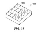
図13は、微細構造フィルム204の代わりに、ディスプレイ装置の一実施形態に含まれてもよい異なる微細構造フィルム1300の斜視図である。微細構造フィルム1300は、四角錐である鋸歯構成1302を備える。各構成1302は、4つの異なる角度方向に入射光を屈折する4つの傾斜面を備える。周辺光は、微細構造フィルム1300において角錐の4つの傾斜面のうちの1つに当たり、4つの角度方向のうちの1つの方向に屈折する。入射光は反射体まで多くの異なる経路をとることから、ピクセルのシャドーイングが低減される。図13に示された例において、4つの側面は等しい面積を有する。その結果、この例の場合には任意のピクセルのシャドーイング作用は、4倍低減される。
FIG. 13 is a perspective view of a different
図14は、微細構造フィルム1404および反射偏光子1408の両方を備える本発明のディスプレイ装置1400の別の実施形態を示している。このディスプレイ装置はまた、第1の偏光子1401と、光変調層1402と、第2の偏光子1403と、光キャビティ1405と、底部反射体1406と、を具備している。補償または位相遅延フィルム1415が、複屈折率の補正または光変調層に関する他の表示特性の改善のために具備されてもよい。
FIG. 14 shows another embodiment of a
図2および図3に関連して上述したように、ディスプレイ装置に微細構造フィルムを備えることにより、ピクセルのシャドーイング作用の低減を生じる。図1に関連して上述したように、反射偏光子1408を備えることにより、光の再循環およびより明るいディスプレイを生じる。底部反射体1406は第1の程度の脱偏光で光を反射し、反射偏光子1408は第2の程度の脱偏光で光を反射する。第2の程度の脱偏光は、少なくとも1つの偏光状態に関して第1の程度の脱偏光より大きい。微細構造フィルム1404は、第1の傾斜面1411および第2の傾斜面1412を備える鋸歯構成1407を備えている。鋸歯構成は、図3に示されたようなプリズムであってもよい。別の実施形態としては、図4の構成と同様に、第2の微細構造フィルムをディスプレイ装置1400に備えたものが考えられる。
As described above in connection with FIGS. 2 and 3, providing the display device with a microstructured film results in reduced pixel shadowing effects. As described above in connection with FIG. 1, the provision of a
図14において、微細構造フィルム1404および反射偏光子1408が、反射偏光子の上部に微細構造フィルム1404を備え、互いから離隔するように配置されている。尚、微細構造フィルム1404の鋸歯構成1407は光変調層1402に面している。微細構造フィルムおよび反射偏光子は、ディスプレイ装置内部で多くの異なる態様に配置され、ピクセルのシャドーイングの低減および光の再循環を依然として実現することができる。微細構造フィルムおよび反射偏光子に関する他の構成の例が数例、図15〜図18に示されている。図15〜図18の構成は、微細構造フィルム1404および反射偏光子1407の代わりに、図14のディスプレイ装置1400内部に用いることも可能である。
In FIG. 14, a
図15に示されているように、反射偏光子1508は、微細構造フィルム1504の上に配置されてもよく、鋸歯構成1507がディスプレイ装置1400の光変調層1402に面する。図16に示されているように、微細構造フィルム1604は反射偏光子1608と結合されてもよく、微細構造フィルム1604の鋸歯構成1607がディスプレイ装置1400の光変調層1402に面する。
As shown in FIG. 15, the
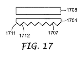
また、鋸歯構成が光変調層とは反対側に面し、依然としてピクセルのシャドーイング作用の低減を実現するように、微細構造フィルムを配置することも可能である。図17に示されているように、反射偏光子1708が、微細構造フィルム1704の上に配置されてもよく、鋸歯構成1707がディスプレイ装置1400の光変調層1402とは反対側に面する。各鋸歯構成1707は、第1の傾斜面1711および第2の傾斜面1712を備える。この構成において周辺光が微細構造フィルム1704を通過するとき、周辺光の入射エネルギーにおける第1の部分が第1の傾斜面1711に当たり、第1の角度方向に屈折する。周辺光の入射エネルギーにおける第2の部分が第2の傾斜面1712に当たり、第2の角度方向に屈折する。周辺光は2つの異なる経路をとるため、周辺光が一部の部分で低減される。微細構造フィルムが図17に示したように、等しい割合で2つのタイプの傾斜面を含んでいる場合には、ピクセルのシャドーイング作用は、2分の1に低減される。
It is also possible to arrange the microstructured film so that the sawtooth configuration faces away from the light modulation layer and still achieves a reduced pixel shadowing effect. As shown in FIG. 17, a
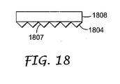
図18に示されているように、微細構造フィルム1807は、反射偏光子1808と結合されてもよく、微細構造フィルム1807の鋸歯構成1807が光変調層1402とは反対側に面するように配置される。この構成は、ディスプレイ装置1400のようなディスプレイ装置に配置される場合には、図17の構造物と同様にピクセルのシャドーイングの低減を実現する。
As shown in FIG. 18, the
図(15および図17)のディスプレイ装置の2つの構成要素の間に、間隙が示されている場合には、一般に、2つの構成要素の間に空隙が存在する。ディスプレイ装置と相互に作用する光が空隙を認識するために、わずか数ミクロンの間隙で十分である。この空隙は、当業界で公知のさまざまな異なる態様で実現されることができる。たとえば、スペーサ素子を用いてもよい。2つの構成要素の面の滑らかさを小さくするために、艶消し層を用いてもよい。構成要素の1つが、図15の場合のような別の素子の平面に隣接して積層されることになっている微細構造フィルムである場合には、微細構造素子は、微細構造素子と隣接する構成要素との間に光学的に十分な空隙を取ることができるように、先端のすべてが同一の高さでなくてもよいように構成することも可能である。 If a gap is shown between the two components of the display device of the figures (15 and 17), there is generally a gap between the two components. A gap of only a few microns is sufficient for the light interacting with the display device to recognize the air gap. This void can be realized in a variety of different ways known in the art. For example, a spacer element may be used. A matte layer may be used to reduce the smoothness of the surfaces of the two components. If one of the components is a microstructured film that is to be laminated adjacent to the plane of another element as in FIG. 15, the microstructure element is adjacent to the microstructure element. It is also possible to configure so that not all of the tips need to be the same height so that an optically sufficient gap can be provided between the components.
図16および図18に示されている構造において、微細構造フィルム1604、1804と反射偏光子1608、1808との間に空隙を有する必要はない。2つの素子を接合または共に結合することができる。また、基板として反射偏光子を用いて、反射偏光子上に直接、微細構造素子を形成することも可能である。
In the structure shown in FIGS. 16 and 18, it is not necessary to have a gap between the
また、微細構造フィルムの代わりに、図14〜図18の構造に含まれるように角錐形状の微細構造フィルム1300を具備することも可能である。別の実施形態としては、図4の構成と同様に、第2の微細構造フィルムを図14〜図18のそれぞれに備えたものが考えられる。
Further, instead of the fine structure film, a pyramid shaped
図5は、透過モードおよび反射モードで作動することができるディスプレイ装置を示している。図5のディスプレイ500は、コレステリック反射偏光子504を具備している。ディスプレイ500はまた、第1の偏光子501と、光変調層502と、第2の偏光子503と、を具備し、第1の偏光子501および第2の偏光子503が光変調層502を包囲している。補償または位相遅延フィルム508が、複屈折率の補正または光変調層に関する他の表示特性の改善のために具備されてもよい。ディスプレイ500はまた、光キャビティ505および底部反射体506を具備している。ディスプレイは、コレステリック反射偏光子504と第2の偏光子503との間に4分の1波長フィルム507をさらに具備している。
FIG. 5 shows a display device that can operate in transmissive and reflective modes. The
透過モードにおいて、光キャビティ505からの光線511が、コレステリック反射偏光子504によって円偏光される。たとえば、右円偏光(RH)光が透過され、左円偏光(LH)光が反射される。透過光の場合には、4分の1波長フィルム507が底部偏光子503によってRH光入力から直線偏光状態を構成する。コレステリック反射偏光子から反射されるLH光の場合には、底部反射体506からの反射時の位相シフトが望ましい。底部反射体506が反射時に位相シフトを生じるように構成される。この位相シフトは、コレステリック反射偏光子504による透過の場合に、LH光をRH光に変換する。高い反射率および位相シフト特性を形成する底部反射体506に関する適切な反射体材料としては、銀およびアルミニウムなどの金属、または有機発光ダイオードに一般に見られる不透明な電極金属が挙げられる。
In the transmissive mode, the
ディスプレイ500がディスプレイを透過する周辺光を用いて照明される反射モードにおいて、入射光510がコレステリック反射偏光子504によって光キャビティ505に透過される。光を出射するために、2つの位相シフトが必要である。たとえば、コレステリック反射偏光子504によって透過されるRH光は、底部反射体506からの反射によってLH光となる。次に、LHは、コレステリック反射偏光子504によって反射され、底部反射体506に戻される。底部反射体506からの第2の反射によって、LH光はRH光に戻るように変換され、最後にコレステリック反射偏光子504によって透過される。この複数回の跳ね返り状態により、横方向のピクセルのシャドーイング分離を強化することができる。ディスプレイ500は、半透過層を備える必要がなく、周辺光または光源からの光を用いて、ディスプレイを形成する。有機発光ダイオードなどの厚みを薄くしたバックライト、適切な拡散層および/または適切な微細構造層をディスプレイ500に備えることは有利であると考えられる。
In the reflective mode, where the
ディスプレイ500は、光源としてフロントライトを備えていてもよく、エッジ照明型光導波路が光を表示円錐において反射体に向かって下方に向けるように構成される。このフロントライトは、図2および図4の微細構造フィルム204と同様に、画像分割機能を提供するように構成されてもよく、それによってピクセルのシャドーイング作用を低減する。
The
コレステリック反射偏光子も備える別のディスプレイにおいて、4分の1波長フィルム507を省略することが可能であり、代わりに、コレステリック反射偏光子層504が4分の1波長フィルムの性能を提供するコーティングを備えることも可能である。
In another display that also includes a cholesteric reflective polarizer, the quarter-
図6〜図12は、本願明細書に記載したディスプレイ装置用の底部反射体の構成を示している。図6〜図12に示された構造は、ディスプレイ100用の底部反射体106、図2のディスプレイ200または図4のディスプレイの底部反射体206または図14の底部反射体1406に用いることが可能である。
6-12 show the configuration of the bottom reflector for the display device described herein. The structure shown in FIGS. 6-12 can be used for the
図6は、鏡面反射を形成する平面ミラー600を示している。平面ミラー600は、適切な基板上の不透明なアルミニウムまたは銀のコーティング、または多層ポリマーミラーであってもよいが、それらに限定されるわけではないミラー層601を備える。保護層(図示せず)が、環境的性能または物理的性能を改善するために、ミラー面に塗布されてもよい。
FIG. 6 shows a
図7は、ミラー層701のための制御した拡散反射を形成するために、テクスチャー加工された面702を備えた拡散ミラー700を示している。ミラー層701はまた、適切な基板上の不透明なアルミニウムまたは銀のコーティング、または多層ポリマーミラーであってもよいが、それらに限定されるわけではない。拡散ミラー700の断層図は、反射時に少なくとも1つの偏光状態を実質的に維持するように構成される。
FIG. 7 shows a diffusing
図8は、ミラー層801および拡散層802を備える拡散ミラー800の断面図を示している。ミラー層801は、図6および図7に関して説明したタイプであってもよい。拡散層802は、粒子を装着したコーティングであってもよいが、それに限定されるわけではない。少なくとも1つの偏光状態を実質的に維持し、所望の拡散を提供するために、粒子サイズ、形状、屈折率、断層図およびコーティングの厚さなどのコーティングの変数をすべて調節することができる。
FIG. 8 shows a cross-sectional view of a
図9は、ミラー層901および反射偏光子902を備えた偏光ミラー900を示している。反射偏光子902は、反射または透過のいずれかまたはその両方において、実質的に偏光状態を維持するものとする。層902に関する適切な例としては、多層分散位相反射偏光子またはコレステリック反射偏光子が挙げられるが、それらに限定されるわけではない。ミラー層901としては、金属コーティング、積層金属フィルム、積層ポリマー多層ミラーまたは交差反射偏光子のいずれかが可能である。適切な接着層は、図示されていないが、分散層に共に接合されるように組込まれてもよい。偏光反射を形成するように反射偏光子層902を向けることができるが、ミラー層901は反射における偏光を維持する必要はない。
FIG. 9 shows a
たとえば、P1偏光を有する光が偏光ミラー900に垂直入射する場合およびミラー層901が反射時に実質的に偏光を維持しない場合には、ミラー層901はP1偏光およびP2偏光の両方の光を反射する。偏光ミラー900が全体として偏光を維持するように、反射偏光子902は、P1偏光の光のみを出射することができるように構成されてもよい。
For example, when light having P1 polarization enters normal to the
図10は、ミラー層1001と、拡散層1002と、反射偏光子1003と、を組込んだ拡散偏光ミラー1000を示している。反射偏光子1003は、図9に関連して説明した反射偏光子902と類似である。拡散層1002は、反射偏光子1003の構造の一面に組込まれてもよく、または分離積層拡散層または拡散接着剤であってもよい。ミラー層1001は、図6および図7に関連して説明したミラー層と類似であってもよい。適切な接着層は、図示されていないが、分散層に共に接合されるように用いられてもよい。反射偏光子1003が偏光反射を形成するように配置されることができるため、拡散層1002およびミラー層1001は偏光を維持する必要はない。図10に示された拡散偏光ミラー1000は、散乱体の軸を分離することができる。さらなる拡散層を反射偏光子層1003の上の拡散偏光ミラー1000に追加することも可能である。拡散偏光ミラー1000の適切な例としては、拡散側が金属コーティングで覆われた3Mによって作製されたDBEF−Mフィルムが挙げられる。
FIG. 10 shows a diffusing
図11は、拡散層1101および反射偏光子1102を組込んだ別の拡散反射偏光子1100を示している。反射偏光子1102は、図9に関連して説明したタイプであってもよい。拡散層1101は、接着剤が示されていないが、マイクロボイド形成フィルムからなる分離積層フィルムであってもよいが、それに限定されるわけではない。
FIG. 11 shows another diffusely
マイクロボイド形成フィルムは、微孔フィルムとも呼ばれ、拡散反射を形成するために拡散反射偏光子1100に備えられてもよい。マイクロボイド形成フィルムは、全体にわたって離隔されたきわめて小さいボイド領域を有するポリマーフィルムである。熱誘導相分離技術を用いて、マイクロボイド形成フィルムを作製することができる。マイクロボイド形成フィルムを作製するために、半結晶質ポリマーおよび溶媒または希釈剤が用いられる。ポリマーおよび希釈剤は、低温で不相溶であるが、より高温では溶液を形成する。ポリマーおよび希釈剤は、加熱され、均質な溶液を形成するまで押出機で共に混合される。次に、この溶液がシートを形成し、冷却される。冷却または急冷工程中、ポリマーは溶液から結晶化してポリマータイフィブリルによって連結された微視的な結晶性の球晶となる。微細構造物のサイズは、さまざまな技術によって操作されることができる。ポリマーが凝固した後、希釈剤を抽出して、フィルムを光の波長のサイズ程度の微細構造物のサイズに適合させるように延伸することによって、2相フィルムを多孔性になすことができ、それによって、単位厚さ当たり、きわめて効率的な反射体にすることができる。
The microvoided film is also referred to as a microporous film, and may be provided in the diffuse
ディスプレイ装置に用いられることが多い1つのマイクロボイド形成フィルムは、BaSO4を装着したポリエチレンテレフタレート(PET)であり、約95%の反射率を有し、厚さ約9ミルである。より好ましくは、反射率が99%を超えることができるマイクロボイドを形成したTiO2装着PETフィルムを用いる。拡散層1101は、反射偏光子層1102の一面に直接、組込まれてもよい。拡散反射偏光子1100の適切な例としては、マイクロボイド形成フィルムに積層された3Mによって作製されたDBEFフィルムであろう。
One microvoided film often used in display devices is polyethylene terephthalate (PET) with BaSO 4 mounted, has a reflectivity of about 95%, and is about 9 mils thick. More preferably, a TiO 2 -attached PET film on which microvoids capable of exceeding 99% reflectivity are used. The diffusion layer 1101 may be incorporated directly on one surface of the
図12は、ブレーズ(blazed)ミラー反射体1200を示している。まばゆいミラー層1201は、傾斜ミラーまたは拡散構造物またはホログラフィック構造物を備えていてもよいが、それらに限定されるわけではない。まばゆいミラー反射体1200は、反射時に偏光を維持することが理想的であるが、ビームステアリング用途において用いるために、反射伝搬方向において角度シフトを形成する。
FIG. 12 shows a blazed
特定のバックライト設計に応じて、完全鏡面反射体またはある程度の拡散反射によって、一様性および明るさを最適化することが望ましいと考えられる。偏光維持の少なくとも1つの軸を維持することにより、この特徴を必要とするディスプレイ装置用の実質的に偏光を維持するバックライトキャビティを有する必要性を満たす。拡散軸は、光導波路のアパーチャを満たすために有用である。実質的な偏光維持軸の拡散外形を制御することにより、周辺の反射の明るさを最大限にするために役立つ。バックライトにおける拡散は、ディスプレイの視角を広くするために望ましい。しかし、明るいディスプレイを有するために、ランベルト反射に比べて、反射におけるゲインを有することも望ましい。ランベルト反射は、すべての方向において等しい強度の光を反射するため、すべての方向から等しく明るく見えると仮定される。十分に広い視角を有し、十分に明るいディスプレイを提供するために、ゲインおよび拡散の関係のバランスをとらなければならない。バックライト反射体に対するわずかな拡散も、画像面から画像反射体の移動のために、視差およびピクセルのシャドーイングを最小限に抑えるために有用である場合がある。 Depending on the particular backlight design, it may be desirable to optimize uniformity and brightness with a perfect specular reflector or some degree of diffuse reflection. By maintaining at least one axis of polarization maintenance, the need to have a backlight cavity that maintains substantially polarization for display devices that require this feature is met. The diffusion axis is useful to fill the aperture of the optical waveguide. Controlling the diffuse profile of the substantial polarization maintaining axis helps to maximize the brightness of the surrounding reflections. Diffusion in the backlight is desirable to increase the viewing angle of the display. However, in order to have a bright display, it is also desirable to have a gain in reflection compared to Lambertian reflection. Lambert reflection is assumed to appear equally bright from all directions because it reflects equal intensity light in all directions. In order to provide a sufficiently bright display with a sufficiently wide viewing angle, the relationship between gain and diffusion must be balanced. Slight diffusion to the backlight reflector may also be useful to minimize parallax and pixel shadowing due to movement of the image reflector from the image plane.
上述の詳説、例およびデータにより、本発明の製造および構成の利用に関する完全な説明を提供する。本発明のさまざまな実施形態は本発明の精神及び範囲を逸脱することなく形成されるため、本発明は以後に添付された特許請求の範囲に属している。 The above detailed description, examples and data provide a complete description of the manufacture and use of the invention. Since the various embodiments of the invention can be made without departing from the spirit and scope of the invention, the invention resides in the claims hereinafter appended.
Claims (50)
第1の偏光層と第2の偏光層との間に光変調層を備える光変調システムと、
光源および反射体を備える等方性光キャビティであって、前記光キャビティが光を前記光変調層に選択的に提供するようになっており、前記光キャビティが入射光の第1の程度の脱偏光を伴って入射光を反射し、前記反射体が周辺光を前記光変調層に反射して、前記反射モードにおいて周辺光のみを用いて前記ディスプレイを照明するように構成される前記光キャビティと、
前記光変調層と前記光キャビティとの間に配置され、第1の偏光を有する入射光の成分を透過し、第2の偏光を有する入射光の成分を反射するようになっている反射偏光子であって、前記第1の偏光の光を提供するために前記第1の程度の脱偏光より大きい第2の程度の脱偏光を伴って前記第2の偏光の光を反射する前記偏光子と、を具備するディスプレイ装置。 A display device capable of displaying information in a reflection mode using only ambient light and a transmission mode using a light source,
A light modulation system comprising a light modulation layer between the first polarizing layer and the second polarizing layer;
An isotropic optical cavity comprising a light source and a reflector, wherein the optical cavity selectively provides light to the light modulation layer, wherein the optical cavity provides a first degree of depolarization of incident light. The optical cavity configured to illuminate the display using only ambient light in the reflection mode, wherein incident light is reflected, and the reflector reflects ambient light to the light modulation layer;
A reflective polarizer disposed between the light modulation layer and the optical cavity and configured to transmit a component of incident light having a first polarization and reflect a component of incident light having a second polarization The polarizer reflecting the second polarized light with a second degree of depolarization greater than the first degree of depolarization to provide the first polarized light; A display device comprising:
光変調層および第1の偏光層を備える光変調システムと、
光を前記光変調層に提供するための光キャビティと、
前記光キャビティの下に位置し、前記光キャビティから光を受光し、光を前記光変調層に向け、前記反射モードにおいて周辺光のみを用いて前記ディスプレイを照明するように配置される反射体と、
前記光キャビティの上かつ、前記光変調システムの下に位置する第1の微細構造フィルムと、を具備し、前記第1の微細構造フィルムが鋸歯構成を備え、前記鋸歯構成のそれぞれが傾斜面を含み、
周辺光が前記第1の微細構造フィルムに当たり、前記周辺光の入射エネルギーにおける第1の部分が第1の角度方向に屈折し、前記周辺光の入射エネルギーにおける第2の部分が前記第1の角度方向とは異なる第2の角度方向に屈折するディスプレイ装置。 A display device capable of displaying information in a reflection mode using only ambient light and a transmission mode using a light source,
A light modulation system comprising a light modulation layer and a first polarizing layer;
An optical cavity for providing light to the light modulating layer;
A reflector positioned below the optical cavity, receiving light from the optical cavity, directing the light to the light modulation layer, and illuminating the display using only ambient light in the reflection mode; ,
A first microstructured film located above the optical cavity and below the light modulation system, wherein the first microstructured film has a sawtooth configuration, each of the sawtooth configurations having an inclined surface. Including
Ambient light strikes the first microstructured film, a first portion in the incident energy of the ambient light is refracted in a first angular direction, and a second portion in the incident energy of the ambient light is the first angle. A display device that refracts in a second angular direction different from the direction.
前記第1の微細構造フィルムを通過した入射光が前記第2の微細構造フィルムに当たり、前記入射光の入射エネルギーにおける第1の部分が第3の角度方向に屈折し、前記入射光の入射エネルギーにおける第2の部分が前記第3の角度方向とは異なる第4の角度方向に屈折する請求項24に記載のディスプレイ装置。 A second microstructured film disposed under the first microstructured film, wherein the second microstructured film comprises a sawtooth configuration, each sawtooth configuration comprising a prism having an inclined surface, The sawtooth configuration of one microstructured film is perpendicular to the sawtooth configuration of the second microstructured film;
Incident light that has passed through the first microstructured film hits the second microstructured film, a first portion of the incident energy of the incident light is refracted in a third angular direction, and the incident energy of the incident light The display device according to claim 24, wherein the second portion is refracted in a fourth angular direction different from the third angular direction.
前記光変調層と前記光キャビティとの間に配置され、第1の偏光を有する入射光の成分を透過し、第2の偏光を有する入射光の成分を反射するようになっている反射偏光子であって、前記第1の偏光の光を提供するために前記第1の程度の脱偏光より大きい第2の程度の脱偏光を伴って前記第2の偏光の光を反射する前記偏光子をさらに備える請求項22に記載のディスプレイ装置。 The optical cavity is isotropic, reflects incident light with a first degree of depolarization of the incident light, the reflector reflects ambient light toward the light modulation layer, and the reflection mode; Is configured to illuminate the display using only ambient light,
A reflective polarizer disposed between the light modulation layer and the optical cavity and configured to transmit a component of incident light having a first polarization and reflect a component of incident light having a second polarization The polarizer reflecting the second polarized light with a second degree of depolarization greater than the first degree of depolarization to provide the first polarized light. The display device according to claim 22, further comprising:
第1の偏光層と第2の偏光層との間に光変調層を備える光変調システムと、
光源および反射体を備える、光を前記光変調層に選択的に提供するようになっている光キャビティと、ここで前記反射体が周辺光を前記光変調層に反射して、前記反射モードにおいて周辺光のみを用いて前記ディスプレイを照明するように構成され、前記光キャビティの前記反射体が反射時に偏光位相シフトを生じ、
前記光変調層と前記光キャビティとの間に配置され、第1の偏光を有する入射光の成分を透過し、第2の偏光を有する入射光の成分を反射するようになされたコレステリック反射偏光子と、を具備するディスプレイ装置。 A display device capable of displaying information in a reflection mode using only ambient light and a transmission mode using a light source,
A light modulation system comprising a light modulation layer between the first polarizing layer and the second polarizing layer;
An optical cavity comprising a light source and a reflector configured to selectively provide light to the light modulation layer, wherein the reflector reflects ambient light to the light modulation layer and in the reflection mode Configured to illuminate the display using only ambient light, and the reflector of the optical cavity produces a polarization phase shift upon reflection;
A cholesteric reflective polarizer disposed between the light modulation layer and the optical cavity and configured to transmit a component of incident light having a first polarization and reflect a component of incident light having a second polarization And a display device.
Applications Claiming Priority (2)
| Application Number | Priority Date | Filing Date | Title |
|---|---|---|---|
| US35868901P | 2001-11-09 | 2001-11-09 | |
| PCT/US2002/034413 WO2003042747A2 (en) | 2001-11-09 | 2002-10-28 | Optical devices having reflective and transmissive modes for display |
Publications (2)
| Publication Number | Publication Date |
|---|---|
| JP2005509899A true JP2005509899A (en) | 2005-04-14 |
| JP2005509899A5 JP2005509899A5 (en) | 2006-01-05 |
Family
ID=23410639
Family Applications (1)
| Application Number | Title | Priority Date | Filing Date |
|---|---|---|---|
| JP2003544520A Withdrawn JP2005509899A (en) | 2001-11-09 | 2002-10-28 | Optical device with reflective and transmissive modes for display |
Country Status (8)
| Country | Link |
|---|---|
| US (1) | US6894821B2 (en) |
| EP (1) | EP1451635A2 (en) |
| JP (1) | JP2005509899A (en) |
| KR (1) | KR20050040855A (en) |
| CN (1) | CN1606712A (en) |
| AU (1) | AU2002340300A1 (en) |
| TW (1) | TWI229769B (en) |
| WO (1) | WO2003042747A2 (en) |
Cited By (1)
| Publication number | Priority date | Publication date | Assignee | Title |
|---|---|---|---|---|
| JP2015507346A (en) * | 2012-02-17 | 2015-03-05 | スリーエム イノベイティブ プロパティズ カンパニー | Backlight guide |
Families Citing this family (34)
| Publication number | Priority date | Publication date | Assignee | Title |
|---|---|---|---|---|
| US6515785B1 (en) * | 1999-04-22 | 2003-02-04 | 3M Innovative Properties Company | Optical devices using reflecting polarizing materials |
| KR100606502B1 (en) | 2003-01-14 | 2006-08-02 | 에이에스엠엘 네델란즈 비.브이. | Level sensor for lithographic apparatus |
| US7236217B2 (en) | 2003-01-16 | 2007-06-26 | 3M Innovative Properties Company | Package of optical films with zero-gap bond outside viewing area |
| US7091661B2 (en) * | 2003-01-27 | 2006-08-15 | 3M Innovative Properties Company | Phosphor based light sources having a reflective polarizer |
| JP2005055481A (en) * | 2003-06-09 | 2005-03-03 | Toyota Industries Corp | Optical element, planar illumination apparatus and display apparatus |
| US7247986B2 (en) * | 2003-06-10 | 2007-07-24 | Samsung Sdi. Co., Ltd. | Organic electro luminescent display and method for fabricating the same |
| US7413336B2 (en) | 2003-08-29 | 2008-08-19 | 3M Innovative Properties Company | Adhesive stacking for multiple optical films |
| US7147358B2 (en) | 2003-12-31 | 2006-12-12 | 3M Innovative Properties Company | Cover removal tab for optical products |
| US20050238852A1 (en) * | 2004-04-23 | 2005-10-27 | Naoki Nakayama | Optical products for displays |
| US7339635B2 (en) | 2005-01-14 | 2008-03-04 | 3M Innovative Properties Company | Pre-stacked optical films with adhesive layer |
| US7777832B2 (en) * | 2005-11-18 | 2010-08-17 | 3M Innovative Properties Company | Multi-function enhancement film |
| KR100961660B1 (en) | 2005-12-21 | 2010-06-09 | 에스케이에너지 주식회사 | Microporous film of semicrystalline polymer and method for preparing the same |
| DE102005061749A1 (en) * | 2005-12-21 | 2007-07-05 | Giesecke & Devrient Gmbh | Optically variable security element for making valuable objects safe has an achromatic reflecting micro-structure taking the form of a mosaic made from achromatic reflecting mosaic elements |
| EP2009471B1 (en) * | 2006-03-30 | 2017-03-15 | Ube Industries, Ltd. | Optical filter |
| US20090079668A1 (en) * | 2007-09-22 | 2009-03-26 | Dennis Liu | Method for measuring readability of screen under sunshine |
| WO2009091365A1 (en) * | 2008-01-17 | 2009-07-23 | Thomson Licensing | Display system |
| US8870436B2 (en) * | 2008-09-17 | 2014-10-28 | 3M Innovative Properties Company | Patterned adhesives for reflectors |
| JP5259501B2 (en) * | 2009-06-11 | 2013-08-07 | 富士フイルム株式会社 | Infrared light reflection plate, infrared light reflective laminated glass, and laminate and laminated glass having a cholesteric liquid crystal layer |
| JP5608385B2 (en) * | 2010-02-08 | 2014-10-15 | デクセリアルズ株式会社 | OPTICAL BODY, MANUFACTURING METHOD THEREFOR, WINDOW MATERIAL, JOINT, AND sunshine blocking device |
| US9523919B2 (en) * | 2011-05-31 | 2016-12-20 | 3M Innovative Properties Company | Methods for making differentially pattern cured microstructured articles |
| CN103137075B (en) * | 2011-12-05 | 2016-03-02 | 联想(北京)有限公司 | Terminal device and display control method |
| KR102596990B1 (en) * | 2012-11-30 | 2023-10-31 | 쓰리엠 이노베이티브 프로퍼티즈 컴파니 | Emissive display with reflective polarizer |
| IL232197B (en) | 2014-04-23 | 2018-04-30 | Lumus Ltd | Compact head-mounted display system |
| KR20170119793A (en) | 2016-04-19 | 2017-10-30 | 삼성디스플레이 주식회사 | Display apparatus |
| CA2992213C (en) | 2016-10-09 | 2023-08-29 | Yochay Danziger | Aperture multiplier using a rectangular waveguide |
| KR20230084335A (en) | 2016-11-08 | 2023-06-12 | 루머스 리미티드 | Light-guide device with optical cutoff edge and corresponding production methods |
| KR102537642B1 (en) | 2017-07-19 | 2023-05-26 | 루머스 리미티드 | LCOS lighting via LOE |
| US11194010B2 (en) * | 2018-05-07 | 2021-12-07 | Omnitek Partners Llc | Non-GPS local full position and orientation referencing system |
| IL259518B2 (en) | 2018-05-22 | 2023-04-01 | Lumus Ltd | Optical system and method for improvement of light field uniformity |
| US11415812B2 (en) | 2018-06-26 | 2022-08-16 | Lumus Ltd. | Compact collimating optical device and system |
| JP7398131B2 (en) | 2019-03-12 | 2023-12-14 | ルムス エルティーディー. | image projector |
| KR20240059655A (en) | 2019-12-08 | 2024-05-07 | 루머스 리미티드 | Optical systems with compact image projector |
| WO2021150813A1 (en) * | 2020-01-24 | 2021-07-29 | Brightview Technologies, Inc. | Optical film for back light unit and back light unit including same |
| CN114114496B (en) * | 2020-08-31 | 2023-03-21 | 宁波激智科技股份有限公司 | Polarization-maintaining optical film and preparation method thereof |
Family Cites Families (19)
| Publication number | Priority date | Publication date | Assignee | Title |
|---|---|---|---|---|
| US6630974B2 (en) | 1991-11-27 | 2003-10-07 | Reveo, Inc. | Super-wide-angle cholesteric liquid crystal based reflective broadband polarizing films |
| US6002829A (en) * | 1992-03-23 | 1999-12-14 | Minnesota Mining And Manufacturing Company | Luminaire device |
| JP3006306B2 (en) * | 1992-09-16 | 2000-02-07 | インターナショナル・ビジネス・マシーンズ・コーポレイション | Optical film and liquid crystal display device using the optical film |
| US5339179A (en) | 1992-10-01 | 1994-08-16 | International Business Machines Corp. | Edge-lit transflective non-emissive display with angled interface means on both sides of light conducting panel |
| CA2178325A1 (en) * | 1993-12-21 | 1995-06-29 | Andrew J. Ouderkirk | Reflective polarizer with brightness enhancement |
| US5751388A (en) | 1995-04-07 | 1998-05-12 | Honeywell Inc. | High efficiency polarized display |
| CA2247625C (en) | 1996-02-29 | 2006-05-30 | Minnesota Mining And Manufacturing Company | Display brightness enhancement film |
| US5825543A (en) | 1996-02-29 | 1998-10-20 | Minnesota Mining And Manufacturing Company | Diffusely reflecting polarizing element including a first birefringent phase and a second phase |
| JPH10260403A (en) * | 1997-01-20 | 1998-09-29 | Seiko Epson Corp | Liquid-crystal device and electronic equipment |
| JP3460588B2 (en) | 1997-09-18 | 2003-10-27 | セイコーエプソン株式会社 | Display device and electronic device using the same |
| JP3580125B2 (en) * | 1998-03-05 | 2004-10-20 | 日東電工株式会社 | Optical element, lighting device and liquid crystal display device |
| JPH11352479A (en) * | 1998-06-12 | 1999-12-24 | Dainippon Printing Co Ltd | Backlight device and transmission type display device |
| US6181394B1 (en) | 1999-01-22 | 2001-01-30 | White Electronic Designs, Corp. | Super bright low reflection liquid crystal display |
| WO2000049453A1 (en) | 1999-02-17 | 2000-08-24 | Central Research Laboratories Limited | Liquid crystal display |
| US6515785B1 (en) | 1999-04-22 | 2003-02-04 | 3M Innovative Properties Company | Optical devices using reflecting polarizing materials |
| JP2001083508A (en) * | 1999-09-14 | 2001-03-30 | Seiko Epson Corp | Display device and electronic instrument using the same |
| WO2001022129A1 (en) * | 1999-09-20 | 2001-03-29 | 3M Innovative Properties Company | Optical films having at least one particle-containing layer |
| US6975455B1 (en) | 2000-04-18 | 2005-12-13 | 3M Innovative Properties Company | Transflective layer for displays |
| JP2001350008A (en) | 2000-06-09 | 2001-12-21 | Sumitomo Chem Co Ltd | Optical member having reflection function and transmission function |
-
2002
- 2002-10-28 EP EP02778649A patent/EP1451635A2/en not_active Withdrawn
- 2002-10-28 KR KR1020047007071A patent/KR20050040855A/en not_active Application Discontinuation
- 2002-10-28 JP JP2003544520A patent/JP2005509899A/en not_active Withdrawn
- 2002-10-28 WO PCT/US2002/034413 patent/WO2003042747A2/en active Application Filing
- 2002-10-28 AU AU2002340300A patent/AU2002340300A1/en not_active Abandoned
- 2002-10-28 US US10/281,582 patent/US6894821B2/en not_active Expired - Lifetime
- 2002-10-28 CN CNA028222377A patent/CN1606712A/en active Pending
- 2002-11-07 TW TW091132773A patent/TWI229769B/en not_active IP Right Cessation
Cited By (1)
| Publication number | Priority date | Publication date | Assignee | Title |
|---|---|---|---|---|
| JP2015507346A (en) * | 2012-02-17 | 2015-03-05 | スリーエム イノベイティブ プロパティズ カンパニー | Backlight guide |
Also Published As
| Publication number | Publication date |
|---|---|
| AU2002340300A1 (en) | 2003-05-26 |
| AU2002340300A8 (en) | 2005-10-13 |
| KR20050040855A (en) | 2005-05-03 |
| WO2003042747A3 (en) | 2003-08-07 |
| TWI229769B (en) | 2005-03-21 |
| TW200300217A (en) | 2003-05-16 |
| US20030090804A1 (en) | 2003-05-15 |
| EP1451635A2 (en) | 2004-09-01 |
| WO2003042747A2 (en) | 2003-05-22 |
| US6894821B2 (en) | 2005-05-17 |
| CN1606712A (en) | 2005-04-13 |
Similar Documents
| Publication | Publication Date | Title |
|---|---|---|
| JP2005509899A (en) | Optical device with reflective and transmissive modes for display | |
| TWI605287B (en) | Display Device | |
| JP3719433B2 (en) | Display device and electronic device | |
| KR101363703B1 (en) | Optical element for lateral light spreading in back-lit displays and system using same | |
| KR101336397B1 (en) | Color mixing illumination unit and optical system using the same | |
| US6975455B1 (en) | Transflective layer for displays | |
| KR100393823B1 (en) | Liquid crystal display | |
| KR100712333B1 (en) | Backlight device and liquid crystal display device including the same | |
| US20100123854A1 (en) | Optical sheet, illuminating device and liquid crystal display device | |
| JP2008547059A (en) | High polarization sensitivity illumination element and system using the same | |
| JP2010262813A (en) | Lighting device, and liquid crystal display device | |
| US6246455B1 (en) | Display device with liquid crystal between reflective polarizers, and a light source illuminating between the polazers | |
| JP2006019027A (en) | Lighting system | |
| JP4353279B2 (en) | Display device and mobile phone | |
| JP4225301B2 (en) | Display device and electronic device | |
| JP4353271B2 (en) | Display device and mobile phone | |
| JP3953078B2 (en) | Display device and electronic device | |
| JP4813705B2 (en) | Liquid crystal display | |
| JP4389963B2 (en) | Display device and mobile phone | |
| JP2022020391A (en) | Planar lighting device | |
| JP4389970B2 (en) | Display device and mobile phone | |
| JP4086087B2 (en) | Display device and electronic device |
Legal Events
| Date | Code | Title | Description |
|---|---|---|---|
| A521 | Request for written amendment filed |
Free format text: JAPANESE INTERMEDIATE CODE: A523 Effective date: 20051005 |
|
| A621 | Written request for application examination |
Free format text: JAPANESE INTERMEDIATE CODE: A621 Effective date: 20051005 |
|
| A761 | Written withdrawal of application |
Free format text: JAPANESE INTERMEDIATE CODE: A761 Effective date: 20080707 |