JP2005296737A - Beat plate - Google Patents
Beat plate Download PDFInfo
- Publication number
- JP2005296737A JP2005296737A JP2004113623A JP2004113623A JP2005296737A JP 2005296737 A JP2005296737 A JP 2005296737A JP 2004113623 A JP2004113623 A JP 2004113623A JP 2004113623 A JP2004113623 A JP 2004113623A JP 2005296737 A JP2005296737 A JP 2005296737A
- Authority
- JP
- Japan
- Prior art keywords
- plate
- porous
- vibrator
- beat
- nickel
- Prior art date
- Legal status (The legal status is an assumption and is not a legal conclusion. Google has not performed a legal analysis and makes no representation as to the accuracy of the status listed.)
- Pending
Links
Images
Classifications
-
- B—PERFORMING OPERATIONS; TRANSPORTING
- B05—SPRAYING OR ATOMISING IN GENERAL; APPLYING FLUENT MATERIALS TO SURFACES, IN GENERAL
- B05B—SPRAYING APPARATUS; ATOMISING APPARATUS; NOZZLES
- B05B17/00—Apparatus for spraying or atomising liquids or other fluent materials, not covered by the preceding groups
- B05B17/04—Apparatus for spraying or atomising liquids or other fluent materials, not covered by the preceding groups operating with special methods
- B05B17/06—Apparatus for spraying or atomising liquids or other fluent materials, not covered by the preceding groups operating with special methods using ultrasonic or other kinds of vibrations
- B05B17/0607—Apparatus for spraying or atomising liquids or other fluent materials, not covered by the preceding groups operating with special methods using ultrasonic or other kinds of vibrations generated by electrical means, e.g. piezoelectric transducers
- B05B17/0638—Apparatus for spraying or atomising liquids or other fluent materials, not covered by the preceding groups operating with special methods using ultrasonic or other kinds of vibrations generated by electrical means, e.g. piezoelectric transducers spray being produced by discharging the liquid or other fluent material through a plate comprising a plurality of orifices
- B05B17/0646—Vibrating plates, i.e. plates being directly subjected to the vibrations, e.g. having a piezoelectric transducer attached thereto
Landscapes
- Special Spraying Apparatus (AREA)
- Apparatuses For Generation Of Mechanical Vibrations (AREA)
Abstract
Description
本発明は、ビートプレートに関する。更に詳細には、本発明はスキンケアに有効な電解水、化粧水、その他の化粧品、薬剤等の噴霧手段に有用なビートプレートに関するものである。 The present invention relates to a beat plate. More specifically, the present invention relates to a beet plate useful for spraying means such as electrolyzed water, lotion, other cosmetics, and drugs effective for skin care.
スキンケア等に有効な電解質水溶液を電解し、陽極側で電解生成されるpHの低い陽極電解水(酸性水)を殺菌や消毒に利用する技術は良く知られている(特許文献1)。また、陰極電解水(アルカリ水)を飲用等に利用する技術も知られている(特許文献2)。 A technique for electrolyzing an aqueous electrolyte solution effective for skin care or the like, and utilizing anode electrolyzed water (acidic water) having a low pH generated by electrolysis on the anode side for sterilization and disinfection is well known (Patent Document 1). Moreover, the technique which utilizes cathodic electrolyzed water (alkaline water) for drinking etc. is also known (patent document 2).
陽極側で生成する陽極電解水には次亜塩素酸が含まれている。次亜塩素酸には強力な酸化作用と塩素化作用があるので、陽極電解水は殺菌や消毒に利用できる。この様な利用方法は医療機関等で普及している。また陽極電解水中に微量に含まれるオゾンや溶存酸素は肉芽生成促進作用を有することから、外科治療の補助としての利用も研究されている。 The anodic electrolyzed water produced on the anode side contains hypochlorous acid. Since hypochlorous acid has a strong oxidizing action and chlorinating action, anodic electrolyzed water can be used for sterilization and disinfection. Such a method of use is prevalent in medical institutions. In addition, ozone and dissolved oxygen contained in a small amount in the anodic electrolyzed water have a granulation-promoting action, so that their use as an aid for surgical treatment is also being studied.
電解水を治療等に使用する場合、通常、電解水を噴霧装置により患部に噴霧する手法が採られる。液体の噴霧装置には、例えば圧電振動子に振動板を固着した超音波発生素子を用いたものが提案されている(特許文献3)。しかしながら、この提案の噴霧装置は、振動板がニッケル金属で構成されているため、陽極電解水のような腐蝕性液体により振動板が腐食を受ける。従って、この提案の噴霧装置を陽極電解水等の腐食性液体の噴霧用に用いると、振動板が腐食される。その結果、噴霧装置の噴霧性能がすぐに低下してしまう。また、治療に用いる陽極電解水中にニッケル金属が混入すると、金属アレルギー症が発症することが危惧される。このため、この提案の噴霧装置は陽極電解水の噴霧には使用できない。 When using electrolyzed water for treatment or the like, a technique of spraying electrolyzed water on the affected area with a spray device is usually employed. As a liquid spraying apparatus, for example, an apparatus using an ultrasonic generation element in which a diaphragm is fixed to a piezoelectric vibrator has been proposed (Patent Document 3). However, in this proposed spraying device, the diaphragm is made of nickel metal, so that the diaphragm is corroded by a corrosive liquid such as anodic electrolyzed water. Therefore, when this proposed spraying device is used for spraying corrosive liquid such as anodic electrolyzed water, the diaphragm is corroded. As a result, the spraying performance of the spraying device is quickly degraded. Moreover, if nickel metal is mixed in the anodic electrolyzed water used for treatment, there is a concern that metal allergy may develop. For this reason, this proposed spraying device cannot be used for spraying anodic electrolyzed water.
上記の問題を解決するため陽極電解水の噴霧装置の振動板には、陽極電解水のような酸性水でも腐蝕しない白金製の多孔板が使用される。しかしながら、白金は極めて高価な金属であるため、白金製の振動板を用いた噴霧装置は製造コストが高くなる問題がある。
本発明は上記事情に鑑みなされたもので、その目的とするところは、電解水のような腐食性の液体、化粧品、薬剤のような多少粘性の高い液体やエマルジョン等の噴霧に用いることができ、且つ、安価な噴霧装置に好適なビートプレートを提供することにある。 The present invention has been made in view of the above circumstances, and is intended to be used for spraying corrosive liquids such as electrolyzed water, slightly viscous liquids such as cosmetics and drugs, and emulsions. And it is providing the beat plate suitable for an inexpensive spraying apparatus.
上記目的を達成する本発明は、以下に記載するものである。 The present invention for achieving the above object is described below.
〔1〕 振動子と前記振動子に連結された多孔板とからなるビートプレートであって、前記多孔板が多孔ニッケル板と前記多孔ニッケル板の表面を被覆して形成されたダイアモンド構造を一部含んだ炭素と水素からなるアモルファス被膜とからなることを特徴とするビートプレート。 [1] A beat plate comprising a vibrator and a porous plate connected to the vibrator, wherein the porous plate partially covers a diamond structure formed by covering the porous nickel plate and the surface of the porous nickel plate. A beat plate comprising an amorphous coating made of carbon and hydrogen.
〔2〕 振動子がピエゾ振動子である〔1〕に記載のビートプレート。 [2] The beat plate according to [1], wherein the vibrator is a piezo vibrator.
〔3〕 多孔板が孔径5〜50μmの細孔を有する〔1〕又は〔2〕に記載のビートプレート。 [3] The beat plate according to [1] or [2], wherein the porous plate has pores having a pore diameter of 5 to 50 μm.
〔4〕 アモルファス被膜が膜厚0.5〜5.0μmである〔1〕乃至〔3〕の何れか1に記載のビートプレート。 [4] The beat plate according to any one of [1] to [3], wherein the amorphous coating has a thickness of 0.5 to 5.0 μm.
〔5〕 〔1〕に記載のビートプレートを噴霧手段に用いた噴霧器。 [5] A sprayer using the beat plate according to [1] as spraying means.
本発明のビートプレートは、多孔ニッケル板とその表面を被覆して形成されたダイアモンド構造を一部含んだ炭素と水素からなるアモルファス被膜とからなる。アモルファス被膜は耐腐食性が高く、そのため、酸性水等の腐蝕性の液体の噴霧装置に用いることができる。 The beat plate of the present invention comprises a porous nickel plate and an amorphous coating made of carbon and hydrogen partially including a diamond structure formed by coating the surface thereof. Amorphous coatings have high corrosion resistance and can therefore be used in spraying apparatus for corrosive liquids such as acidic water.
また、多孔板に高価な白金を用いていないので、本発明のビートプレートを用いた腐蝕性液体用の噴霧装置は経済性に優れる。更に、本発明のビートプレートの多孔ニッケル板はニッケル板を基材として用いて製造しているので、振動特性が良く腐蝕性液体や高粘度液体、エマルジョン等を効率良く噴霧できる。また、基材のニッケル板は細孔を施す加工が容易である。 Further, since expensive platinum is not used for the perforated plate, the spraying device for corrosive liquid using the beat plate of the present invention is excellent in economy. Furthermore, since the porous nickel plate of the beat plate of the present invention is manufactured using a nickel plate as a base material, it has good vibration characteristics and can efficiently spray corrosive liquids, high viscosity liquids, emulsions and the like. Further, the nickel plate as the base material is easy to process to form pores.
以下、図面を参照しながら本発明を詳細に説明する。 Hereinafter, the present invention will be described in detail with reference to the drawings.
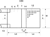
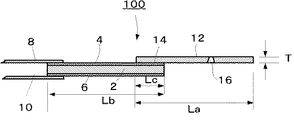
図1は本発明のビートプレートの一例を示す平面図、図2は図1のa−a線に沿う断面図である。 FIG. 1 is a plan view showing an example of a beat plate of the present invention, and FIG. 2 is a cross-sectional view taken along the line aa in FIG.
図2中、100はビートプレートで、2は平板状の振動子である。この振動子2は両表面に電圧を印加することにより振動する素子で、水晶板等のピエゾ素子からなる。
In FIG. 2, 100 is a beat plate and 2 is a flat plate-like vibrator. The
前記振動子2の両面にはそれぞれ電極4、6が形成されている。電極4、6の一端側にはそれぞれ端子8、10が接続されている。前記電極4の他端側には、多孔板12の一端側が固着部14で接合されている。多孔板12には多数の細孔16が形成されている。細孔の孔径は、5〜50μmが好ましく、細孔の密度は1cm2 あたり6000〜15000個であることが好ましい。
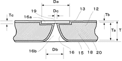
図3は多孔板12の細孔16近傍の拡大断面図である。図3中、18は多孔ニッケル板で、ニッケル製の平板に多数の細孔16が形成してある。前記多孔ニッケル板18の表面はアモルファス被膜20で被覆されている。
FIG. 3 is an enlarged cross-sectional view of the vicinity of the
図3に示すように、多孔板12の一面13には所定深さ(Tc)の円板状第一孔16aが穿設されている。
As shown in FIG. 3, a disk-shaped
前記第一孔16aの底面には第一孔の径(Da)よりも小径(Dc)で、他面に向うに従って徐々に大径に至る第二孔16bが穿設されている。この第二孔16bは、その側面の断面形状が内側に凸となる緩やかな曲線で形成され、この曲線は他面15に漸近している。
A
前記細孔16は、第一孔底部19と他面15とで細孔径Dc、Dbが異なっており、本図においては、最小径Dcは他面径Dbの1/10に形成されている。この最小径Dcと他面径Dbの比は1/2〜1/10であることが好ましい。また、細孔16は、一面13と他面15とで一面径Da、他面径Dbが略同一に形成されている。尚、前記第一孔16aの深さ(Tc)は、多孔板の厚みTの約1/10である。
The
本発明における多孔板12は、例えば、多孔ニッケル板18の表面を当業者が公知の方法で、ダイアモンド構造を一部含んだ炭素と水素からなるアモルファス被膜20で被覆することにより作製することができる。この被覆方法としては、高真空下に炭化水素を充満させた雰囲気に多孔ニッケル板18を入れ、プラズマ処理する方法を例示することができる。アモルファス被膜20の被膜厚み(Tb)は、0.5〜5.0μmであることが好ましい。また、多孔ニッケル板の厚み(Ta)は0.02〜1.0mmであることが好ましい。アモルファス被膜20の被膜厚み(Tb)が上記の範囲であると、多孔ニッケル板18を電解水による腐食から長期に亘り保護できる。また、経済性にも優れる。尚、ダイアモンド構造を一部含んだ炭素と水素からなるアモルファス被膜20は、通称DLC(Diamond like Carbon)で表わされている。
The
また、アモルファス被膜20の蒸着に用いる多孔ニッケル板18には、ニッケル板に当業者が公知の方法で細孔を多数穿孔したものを用いることができる。この穿孔方法としては、例えば、以下に述べる電鋳法を挙げることができる。
The
即ち、ステンレス板の片面にレジストを塗布し、フォトレジスト法にて円柱状の硬化レジストが多数存在するステンレス板を得る。次いでこのステンレス板上にニッケルメッキを施し、更に、ニッケルメッキ部分をステンレス金属面及び硬化レジスト面から剥離して、多数の貫通孔が形成されたニッケル板を得る。 That is, a resist is applied to one surface of a stainless steel plate, and a stainless steel plate having a large number of cylindrical hardened resists is obtained by a photoresist method. Next, nickel plating is performed on the stainless steel plate, and the nickel plated portion is peeled off from the stainless steel metal surface and the hardened resist surface to obtain a nickel plate in which a large number of through holes are formed.
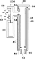
図4は電解槽38及び、電解槽38に結合した噴霧手段200を示す拡大図である。電解槽38は、扁平な電解槽筐体42内に、平行に配設された陽極44、及び陰極46を有する。なお、48は陽極44に接続された陽極端子、50は陰極46に接続された陰極端子である。
FIG. 4 is an enlarged view showing the
ポンプ(図示していない)から供給される電解原料水は、電解槽38の下部に形成された流入孔52から電解槽38内に供給され、層流状態を保ちながら槽内を上方に移動すると共に陽極44、陰極46間に印加されている電圧により電気分解され、陽極44近傍には酸性水が生成し、陰極46近傍にはアルカリ性水が生成する。
Electrolytic raw water supplied from a pump (not shown) is supplied into the
電解槽38内の電解原料水は層流状態で流れているので、生成した酸性水は陽極44の表面に沿って矢印Aで示される様に上方に流れ、酸性水のみが電解槽38の上部側に形成された取出し孔54を通って噴霧手段200の噴霧室56に供給される。
Since the electrolytic raw material water in the
58は多孔板で、これにより噴霧手段200の噴霧室56と外界とが分離されている。前記多孔板58は、孔径18〜24μmの細孔が多数形成されていると共に、この多孔板58はピエゾ振動子60に固定されている。従って、このピエゾ振動子60に交流やパルス電圧が印加される事により振動子60が振動し、これに伴い振動子60に連結された多孔板58が振動する。これにより、噴霧室56内に充満された酸性水が多孔板58に形成された細孔を通して外部に微細液滴62として噴霧される。
A
一方、電解槽38内で生成したアルカリ性水は、矢印Bにより示されるように、陰極46に沿って上方に移動し、廃液口64を通ってアルカリ性水貯槽(図示していない)に蓄えられる。
On the other hand, the alkaline water generated in the
本発明を実施例により更に説明する。 The invention is further illustrated by the examples.
図1及び図2に示すビートプレート100を下記の通り作製した。
The
電鋳法により、厚みが1.0mm、幅が20mm、長さが17mmの多数の細孔を有する矩形多孔ニッケル板18を作製した。穿孔した細孔の平均直径は、一面での直径が約100μm、他面での直径が約100μm、最小径部での直径が約10μm、第一孔の深さが約0.1mmであり、細孔の設置密度は1cm2 当たり6500個とした。
A rectangular
次いで、この多孔ニッケル板18をプラズマ処理器内に入れ、器内を1×10⁻³Paの高真空とした後、器内にメタンガスを導入し、プラズマ処理により多孔ニッケル板の全表面にダイアモンド構造を一部含んだ炭素と水素からなるアモルファス被膜20を形成さて多孔板12を得た。アモルファス被膜20の被膜厚み(Tb)は、0.5μmとした。
Next, the
次に、得られた多孔板12の一端を長さ(Lb)が19mmの振動子3の一端と固着部6の長さ(Lc)が3mmとなるように固着させビートプレート100を得た。
Next, one end of the obtained
得られたビートプレート100は、多孔板12の幅(W)が20mm、多孔板2の長さ(La)が17mm、多孔板2の厚み(T)が1.0mm、振動子3の長さ(Lb)が22mmである。多孔板2、振動子3と固着部6の寸法は、ビートプレート100を噴霧器の部品として用いるための実用上適度な寸法にしてある。
The obtained beat
多孔板12に施された細孔16は、多孔板の一面13での直径(Da)が平均100μm、多孔板の他面15での直径(Db)が平均100μm、第一孔底部での直径(Dc)が平均20μm、第一孔の深さ(Tc)が平均0.1mmである。また、細孔16の設置密度は、多孔板1cm2 当たり6500個である。上記細孔16の寸法(Da、Db、Dc、Tc)、設置密度は、ビートプレート100を電解水用噴霧器の部品として用いた際に、治療上適度な量及びサイズの霧状電解水を噴霧器から発生できるように設定してある。
The
このようにして得られた多孔板12の表面を被覆しているアモルファス被膜20(DLC)の酸性溶液に対する耐性評価を行った。多孔板12の部分を秤量後、pH2.0の希塩酸(15ml)中に室温(20〜25℃)にて300時間浸漬させた。次いで、多孔板12を取り出し、水洗、乾燥後、質量測定と表面観察を行った。その結果、多孔板12の質量変化は全く無く、また多孔板表面のDLC外観に変化は認められなかった。
Thus, the tolerance evaluation with respect to the acidic solution of the amorphous film 20 (DLC) which coat | covers the surface of the
100 ビートプレート
2 振動子
4、6 電極
8、10 端子
12 多孔板
13 多孔板の一面
14 固着部
15 多孔板の他面
16 細孔
16a 細孔の第一孔
16b 細孔の第二孔
18 多孔ニッケル板
19 細孔第一孔の底部
20 アモルファス被膜
200 噴霧手段
38 電解槽
42 電解槽筐体
44 陽極
46 陰極
48 陽極端子
50 陰極端子
52 流入孔
54 取出孔
56 噴霧室
58 多孔板
60 ピエゾ振動子
62 液滴
T 多孔板の厚み
Ta 多孔ニッケル板の厚み
Tb アモルファス被膜の厚み
Tc 細孔の第一孔の深さ
Da 細孔の一端の直径
Db 細孔の他端の直径
Dc 細孔の最小径部の直径
W 多孔板の幅
La 多孔板の長さ
Lb 振動子の長さ
Lc 固着部の長さ
DESCRIPTION OF
Claims (5)
Priority Applications (1)
| Application Number | Priority Date | Filing Date | Title |
|---|---|---|---|
| JP2004113623A JP2005296737A (en) | 2004-04-07 | 2004-04-07 | Beat plate |
Applications Claiming Priority (1)
| Application Number | Priority Date | Filing Date | Title |
|---|---|---|---|
| JP2004113623A JP2005296737A (en) | 2004-04-07 | 2004-04-07 | Beat plate |
Publications (1)
| Publication Number | Publication Date |
|---|---|
| JP2005296737A true JP2005296737A (en) | 2005-10-27 |
Family
ID=35328935
Family Applications (1)
| Application Number | Title | Priority Date | Filing Date |
|---|---|---|---|
| JP2004113623A Pending JP2005296737A (en) | 2004-04-07 | 2004-04-07 | Beat plate |
Country Status (1)
| Country | Link |
|---|---|
| JP (1) | JP2005296737A (en) |
Cited By (63)
| Publication number | Priority date | Publication date | Assignee | Title |
|---|---|---|---|---|
| JP2012004871A (en) * | 2010-06-17 | 2012-01-05 | Yasuo Kondo | Ultrasonic horn |
| US8137466B2 (en) | 2009-08-24 | 2012-03-20 | Samsung Mobile Display Co., Ltd. | Thin film deposition apparatus and method of manufacturing organic light-emitting display device by using the same |
| US8486737B2 (en) | 2009-08-25 | 2013-07-16 | Samsung Display Co., Ltd. | Thin film deposition apparatus and method of manufacturing organic light-emitting display device by using the same |
| US8536057B2 (en) | 2009-06-25 | 2013-09-17 | Samsung Display Co., Ltd. | Thin film deposition apparatus and method of manufacturing organic light emitting device by using the same |
| US8707889B2 (en) | 2011-05-25 | 2014-04-29 | Samsung Display Co., Ltd. | Patterning slit sheet assembly, organic layer deposition apparatus, method of manufacturing organic light-emitting display apparatus, and the organic light-emitting display apparatus |
| US8709161B2 (en) | 2009-08-05 | 2014-04-29 | Samsung Display Co., Ltd. | Thin film deposition apparatus and method of manufacturing organic light-emitting display device by using the same |
| US8802200B2 (en) | 2009-06-09 | 2014-08-12 | Samsung Display Co., Ltd. | Method and apparatus for cleaning organic deposition materials |
| US8833294B2 (en) | 2010-07-30 | 2014-09-16 | Samsung Display Co., Ltd. | Thin film deposition apparatus including patterning slit sheet and method of manufacturing organic light-emitting display device with the same |
| US8846547B2 (en) | 2010-09-16 | 2014-09-30 | Samsung Display Co., Ltd. | Thin film deposition apparatus, method of manufacturing organic light-emitting display device by using the thin film deposition apparatus, and organic light-emitting display device manufactured by using the method |
| US8852687B2 (en) | 2010-12-13 | 2014-10-07 | Samsung Display Co., Ltd. | Organic layer deposition apparatus |
| US8859043B2 (en) | 2011-05-25 | 2014-10-14 | Samsung Display Co., Ltd. | Organic layer deposition apparatus and method of manufacturing organic light-emitting display device by using the same |
| US8859325B2 (en) | 2010-01-14 | 2014-10-14 | Samsung Display Co., Ltd. | Thin film deposition apparatus, method of manufacturing organic light-emitting display device by using the apparatus, and organic light-emitting display device manufactured by using the method |
| US8865252B2 (en) | 2010-04-06 | 2014-10-21 | Samsung Display Co., Ltd. | Thin film deposition apparatus and method of manufacturing organic light-emitting display device by using the same |
| US8871542B2 (en) | 2010-10-22 | 2014-10-28 | Samsung Display Co., Ltd. | Method of manufacturing organic light emitting display apparatus, and organic light emitting display apparatus manufactured by using the method |
| US8876975B2 (en) | 2009-10-19 | 2014-11-04 | Samsung Display Co., Ltd. | Thin film deposition apparatus |
| US8882921B2 (en) | 2009-06-08 | 2014-11-11 | Samsung Display Co., Ltd. | Thin film deposition apparatus |
| US8882922B2 (en) | 2010-11-01 | 2014-11-11 | Samsung Display Co., Ltd. | Organic layer deposition apparatus |
| US8882556B2 (en) | 2010-02-01 | 2014-11-11 | Samsung Display Co., Ltd. | Thin film deposition apparatus, method of manufacturing organic light-emitting display device by using the apparatus, and organic light-emitting display device manufactured by using the method |
| US8882920B2 (en) | 2009-06-05 | 2014-11-11 | Samsung Display Co., Ltd. | Thin film deposition apparatus |
| US8894458B2 (en) | 2010-04-28 | 2014-11-25 | Samsung Display Co., Ltd. | Thin film deposition apparatus, method of manufacturing organic light-emitting display device by using the apparatus, and organic light-emitting display device manufactured by using the method |
| US8907326B2 (en) | 2009-06-24 | 2014-12-09 | Samsung Display Co., Ltd. | Organic light-emitting display device and thin film deposition apparatus for manufacturing the same |
| US8906731B2 (en) | 2011-05-27 | 2014-12-09 | Samsung Display Co., Ltd. | Patterning slit sheet assembly, organic layer deposition apparatus, method of manufacturing organic light-emitting display apparatus, and the organic light-emitting display apparatus |
| US8916237B2 (en) | 2009-05-22 | 2014-12-23 | Samsung Display Co., Ltd. | Thin film deposition apparatus and method of depositing thin film |
| US8921831B2 (en) | 2009-08-24 | 2014-12-30 | Samsung Display Co., Ltd. | Thin film deposition apparatus, method of manufacturing organic light-emitting display device by using the apparatus, and organic light-emitting display device manufactured by using the method |
| WO2015011608A1 (en) * | 2013-07-22 | 2015-01-29 | Koninklijke Philips N.V. | A mesh for use in a nebuliser, and a method of manufacturing the same |
| US8945974B2 (en) | 2012-09-20 | 2015-02-03 | Samsung Display Co., Ltd. | Method of manufacturing organic light-emitting display device using an organic layer deposition apparatus |
| US8945979B2 (en) | 2012-11-09 | 2015-02-03 | Samsung Display Co., Ltd. | Organic layer deposition apparatus, method of manufacturing organic light-emitting display apparatus by using the same, and organic light-emitting display apparatus manufactured by the method |
| US8951610B2 (en) | 2011-07-04 | 2015-02-10 | Samsung Display Co., Ltd. | Organic layer deposition apparatus |
| US8951349B2 (en) | 2009-11-20 | 2015-02-10 | Samsung Display Co., Ltd. | Thin film deposition apparatus and method of manufacturing organic light-emitting display device by using the same |
| US8956697B2 (en) | 2012-07-10 | 2015-02-17 | Samsung Display Co., Ltd. | Method of manufacturing organic light-emitting display apparatus and organic light-emitting display apparatus manufactured by using the method |
| US8962360B2 (en) | 2013-06-17 | 2015-02-24 | Samsung Display Co., Ltd. | Organic layer deposition apparatus and method of manufacturing organic light-emitting display device by using the organic layer deposition apparatus |
| US8968829B2 (en) | 2009-08-25 | 2015-03-03 | Samsung Display Co., Ltd. | Thin film deposition apparatus and method of manufacturing organic light-emitting display device by using the same |
| US8973525B2 (en) | 2010-03-11 | 2015-03-10 | Samsung Display Co., Ltd. | Thin film deposition apparatus |
| US8993360B2 (en) | 2013-03-29 | 2015-03-31 | Samsung Display Co., Ltd. | Deposition apparatus, method of manufacturing organic light emitting display apparatus, and organic light emitting display apparatus |
| US9012258B2 (en) | 2012-09-24 | 2015-04-21 | Samsung Display Co., Ltd. | Method of manufacturing an organic light-emitting display apparatus using at least two deposition units |
| US9018647B2 (en) | 2010-09-16 | 2015-04-28 | Samsung Display Co., Ltd. | Thin film deposition apparatus, method of manufacturing organic light-emitting display device by using the apparatus, and organic light-emitting display device manufactured by using the method |
| US9040330B2 (en) | 2013-04-18 | 2015-05-26 | Samsung Display Co., Ltd. | Method of manufacturing organic light-emitting display apparatus |
| US9051636B2 (en) | 2011-12-16 | 2015-06-09 | Samsung Display Co., Ltd. | Organic layer deposition apparatus, method of manufacturing organic light-emitting display apparatus using the same, and organic light-emitting display apparatus |
| US9121095B2 (en) | 2009-05-22 | 2015-09-01 | Samsung Display Co., Ltd. | Thin film deposition apparatus |
| US9136476B2 (en) | 2013-03-20 | 2015-09-15 | Samsung Display Co., Ltd. | Method of manufacturing organic light-emitting display apparatus, and organic light-emitting display apparatus manufactured by the method |
| US9150952B2 (en) | 2011-07-19 | 2015-10-06 | Samsung Display Co., Ltd. | Deposition source and deposition apparatus including the same |
| US9174250B2 (en) | 2009-06-09 | 2015-11-03 | Samsung Display Co., Ltd. | Method and apparatus for cleaning organic deposition materials |
| US9206501B2 (en) | 2011-08-02 | 2015-12-08 | Samsung Display Co., Ltd. | Method of manufacturing organic light-emitting display apparatus by using an organic layer deposition apparatus having stacked deposition sources |
| US9234270B2 (en) | 2011-05-11 | 2016-01-12 | Samsung Display Co., Ltd. | Electrostatic chuck, thin film deposition apparatus including the electrostatic chuck, and method of manufacturing organic light emitting display apparatus by using the thin film deposition apparatus |
| US9249493B2 (en) | 2011-05-25 | 2016-02-02 | Samsung Display Co., Ltd. | Organic layer deposition apparatus and method of manufacturing organic light-emitting display apparatus by using the same |
| US9257649B2 (en) | 2012-07-10 | 2016-02-09 | Samsung Display Co., Ltd. | Method of manufacturing organic layer on a substrate while fixed to electrostatic chuck and charging carrier using contactless power supply module |
| US9260778B2 (en) | 2012-06-22 | 2016-02-16 | Samsung Display Co., Ltd. | Organic layer deposition apparatus, method of manufacturing organic light-emitting display apparatus using the same, and organic light-emitting display apparatus manufactured using the method |
| US9279177B2 (en) | 2010-07-07 | 2016-03-08 | Samsung Display Co., Ltd. | Thin film deposition apparatus, method of manufacturing organic light-emitting display device by using the apparatus, and organic light-emitting display device manufactured by using the method |
| US9306191B2 (en) | 2012-10-22 | 2016-04-05 | Samsung Display Co., Ltd. | Organic light-emitting display apparatus and method of manufacturing the same |
| US9347886B2 (en) | 2013-06-24 | 2016-05-24 | Samsung Display Co., Ltd. | Apparatus for monitoring deposition rate, apparatus provided with the same for depositing organic layer, method of monitoring deposition rate, and method of manufacturing organic light emitting display apparatus using the same |
| US9388488B2 (en) | 2010-10-22 | 2016-07-12 | Samsung Display Co., Ltd. | Organic film deposition apparatus and method of manufacturing organic light-emitting display device by using the same |
| US9450140B2 (en) | 2009-08-27 | 2016-09-20 | Samsung Display Co., Ltd. | Thin film deposition apparatus and method of manufacturing organic light-emitting display apparatus using the same |
| US9461277B2 (en) | 2012-07-10 | 2016-10-04 | Samsung Display Co., Ltd. | Organic light emitting display apparatus |
| US9466647B2 (en) | 2012-07-16 | 2016-10-11 | Samsung Display Co., Ltd. | Flat panel display device and method of manufacturing the same |
| US9496317B2 (en) | 2013-12-23 | 2016-11-15 | Samsung Display Co., Ltd. | Method of manufacturing organic light emitting display apparatus |
| US9496524B2 (en) | 2012-07-10 | 2016-11-15 | Samsung Display Co., Ltd. | Organic layer deposition apparatus, method of manufacturing organic light-emitting display apparatus using the same, and organic light-emitting display apparatus manufactured using the method |
| US9512515B2 (en) | 2011-07-04 | 2016-12-06 | Samsung Display Co., Ltd. | Organic layer deposition apparatus and method of manufacturing organic light-emitting display device by using the same |
| US9534288B2 (en) | 2013-04-18 | 2017-01-03 | Samsung Display Co., Ltd. | Deposition apparatus, method of manufacturing organic light-emitting display apparatus by using same, and organic light-emitting display apparatus manufactured by using deposition apparatus |
| US9593408B2 (en) | 2009-08-10 | 2017-03-14 | Samsung Display Co., Ltd. | Thin film deposition apparatus including deposition blade |
| US9624580B2 (en) | 2009-09-01 | 2017-04-18 | Samsung Display Co., Ltd. | Thin film deposition apparatus |
| US9748483B2 (en) | 2011-01-12 | 2017-08-29 | Samsung Display Co., Ltd. | Deposition source and organic layer deposition apparatus including the same |
| KR20180002493A (en) * | 2016-06-29 | 2018-01-08 | 동국대학교 경주캠퍼스 산학협력단 | Manufacturing method of microporous filter for aerosol generating nebulizer and microporous filter by using thereof |
| US10246769B2 (en) | 2010-01-11 | 2019-04-02 | Samsung Display Co., Ltd. | Thin film deposition apparatus |
-
2004
- 2004-04-07 JP JP2004113623A patent/JP2005296737A/en active Pending
Cited By (78)
| Publication number | Priority date | Publication date | Assignee | Title |
|---|---|---|---|---|
| US8916237B2 (en) | 2009-05-22 | 2014-12-23 | Samsung Display Co., Ltd. | Thin film deposition apparatus and method of depositing thin film |
| US9121095B2 (en) | 2009-05-22 | 2015-09-01 | Samsung Display Co., Ltd. | Thin film deposition apparatus |
| US8882920B2 (en) | 2009-06-05 | 2014-11-11 | Samsung Display Co., Ltd. | Thin film deposition apparatus |
| US8882921B2 (en) | 2009-06-08 | 2014-11-11 | Samsung Display Co., Ltd. | Thin film deposition apparatus |
| US8802200B2 (en) | 2009-06-09 | 2014-08-12 | Samsung Display Co., Ltd. | Method and apparatus for cleaning organic deposition materials |
| US9174250B2 (en) | 2009-06-09 | 2015-11-03 | Samsung Display Co., Ltd. | Method and apparatus for cleaning organic deposition materials |
| US8907326B2 (en) | 2009-06-24 | 2014-12-09 | Samsung Display Co., Ltd. | Organic light-emitting display device and thin film deposition apparatus for manufacturing the same |
| US8536057B2 (en) | 2009-06-25 | 2013-09-17 | Samsung Display Co., Ltd. | Thin film deposition apparatus and method of manufacturing organic light emitting device by using the same |
| US8709161B2 (en) | 2009-08-05 | 2014-04-29 | Samsung Display Co., Ltd. | Thin film deposition apparatus and method of manufacturing organic light-emitting display device by using the same |
| US9593408B2 (en) | 2009-08-10 | 2017-03-14 | Samsung Display Co., Ltd. | Thin film deposition apparatus including deposition blade |
| US8921831B2 (en) | 2009-08-24 | 2014-12-30 | Samsung Display Co., Ltd. | Thin film deposition apparatus, method of manufacturing organic light-emitting display device by using the apparatus, and organic light-emitting display device manufactured by using the method |
| US8193011B2 (en) | 2009-08-24 | 2012-06-05 | Samsung Mobile Display Co., Ltd. | Thin film deposition apparatus and method of manufacturing organic light-emitting display device by using the same |
| US8137466B2 (en) | 2009-08-24 | 2012-03-20 | Samsung Mobile Display Co., Ltd. | Thin film deposition apparatus and method of manufacturing organic light-emitting display device by using the same |
| US8968829B2 (en) | 2009-08-25 | 2015-03-03 | Samsung Display Co., Ltd. | Thin film deposition apparatus and method of manufacturing organic light-emitting display device by using the same |
| US8486737B2 (en) | 2009-08-25 | 2013-07-16 | Samsung Display Co., Ltd. | Thin film deposition apparatus and method of manufacturing organic light-emitting display device by using the same |
| US9450140B2 (en) | 2009-08-27 | 2016-09-20 | Samsung Display Co., Ltd. | Thin film deposition apparatus and method of manufacturing organic light-emitting display apparatus using the same |
| US9624580B2 (en) | 2009-09-01 | 2017-04-18 | Samsung Display Co., Ltd. | Thin film deposition apparatus |
| US8876975B2 (en) | 2009-10-19 | 2014-11-04 | Samsung Display Co., Ltd. | Thin film deposition apparatus |
| US9224591B2 (en) | 2009-10-19 | 2015-12-29 | Samsung Display Co., Ltd. | Method of depositing a thin film |
| US8951349B2 (en) | 2009-11-20 | 2015-02-10 | Samsung Display Co., Ltd. | Thin film deposition apparatus and method of manufacturing organic light-emitting display device by using the same |
| US9660191B2 (en) | 2009-11-20 | 2017-05-23 | Samsung Display Co., Ltd. | Thin film deposition apparatus and method of manufacturing organic light-emitting display device by using the same |
| US10246769B2 (en) | 2010-01-11 | 2019-04-02 | Samsung Display Co., Ltd. | Thin film deposition apparatus |
| US10287671B2 (en) | 2010-01-11 | 2019-05-14 | Samsung Display Co., Ltd. | Thin film deposition apparatus |
| US8859325B2 (en) | 2010-01-14 | 2014-10-14 | Samsung Display Co., Ltd. | Thin film deposition apparatus, method of manufacturing organic light-emitting display device by using the apparatus, and organic light-emitting display device manufactured by using the method |
| US8882556B2 (en) | 2010-02-01 | 2014-11-11 | Samsung Display Co., Ltd. | Thin film deposition apparatus, method of manufacturing organic light-emitting display device by using the apparatus, and organic light-emitting display device manufactured by using the method |
| US9453282B2 (en) | 2010-03-11 | 2016-09-27 | Samsung Display Co., Ltd. | Thin film deposition apparatus |
| US8973525B2 (en) | 2010-03-11 | 2015-03-10 | Samsung Display Co., Ltd. | Thin film deposition apparatus |
| US8865252B2 (en) | 2010-04-06 | 2014-10-21 | Samsung Display Co., Ltd. | Thin film deposition apparatus and method of manufacturing organic light-emitting display device by using the same |
| US8894458B2 (en) | 2010-04-28 | 2014-11-25 | Samsung Display Co., Ltd. | Thin film deposition apparatus, method of manufacturing organic light-emitting display device by using the apparatus, and organic light-emitting display device manufactured by using the method |
| US9136310B2 (en) | 2010-04-28 | 2015-09-15 | Samsung Display Co., Ltd. | Thin film deposition apparatus, method of manufacturing organic light-emitting display device by using the apparatus, and organic light-emitting display device manufactured by using the method |
| JP2012004871A (en) * | 2010-06-17 | 2012-01-05 | Yasuo Kondo | Ultrasonic horn |
| US9279177B2 (en) | 2010-07-07 | 2016-03-08 | Samsung Display Co., Ltd. | Thin film deposition apparatus, method of manufacturing organic light-emitting display device by using the apparatus, and organic light-emitting display device manufactured by using the method |
| US8833294B2 (en) | 2010-07-30 | 2014-09-16 | Samsung Display Co., Ltd. | Thin film deposition apparatus including patterning slit sheet and method of manufacturing organic light-emitting display device with the same |
| US8846547B2 (en) | 2010-09-16 | 2014-09-30 | Samsung Display Co., Ltd. | Thin film deposition apparatus, method of manufacturing organic light-emitting display device by using the thin film deposition apparatus, and organic light-emitting display device manufactured by using the method |
| US9018647B2 (en) | 2010-09-16 | 2015-04-28 | Samsung Display Co., Ltd. | Thin film deposition apparatus, method of manufacturing organic light-emitting display device by using the apparatus, and organic light-emitting display device manufactured by using the method |
| US9388488B2 (en) | 2010-10-22 | 2016-07-12 | Samsung Display Co., Ltd. | Organic film deposition apparatus and method of manufacturing organic light-emitting display device by using the same |
| US8871542B2 (en) | 2010-10-22 | 2014-10-28 | Samsung Display Co., Ltd. | Method of manufacturing organic light emitting display apparatus, and organic light emitting display apparatus manufactured by using the method |
| US8882922B2 (en) | 2010-11-01 | 2014-11-11 | Samsung Display Co., Ltd. | Organic layer deposition apparatus |
| US8852687B2 (en) | 2010-12-13 | 2014-10-07 | Samsung Display Co., Ltd. | Organic layer deposition apparatus |
| US9748483B2 (en) | 2011-01-12 | 2017-08-29 | Samsung Display Co., Ltd. | Deposition source and organic layer deposition apparatus including the same |
| US9234270B2 (en) | 2011-05-11 | 2016-01-12 | Samsung Display Co., Ltd. | Electrostatic chuck, thin film deposition apparatus including the electrostatic chuck, and method of manufacturing organic light emitting display apparatus by using the thin film deposition apparatus |
| US8859043B2 (en) | 2011-05-25 | 2014-10-14 | Samsung Display Co., Ltd. | Organic layer deposition apparatus and method of manufacturing organic light-emitting display device by using the same |
| US9076982B2 (en) | 2011-05-25 | 2015-07-07 | Samsung Display Co., Ltd. | Patterning slit sheet assembly, organic layer deposition apparatus, method of manufacturing organic light-emitting display apparatus, and the organic light-emitting display apparatus |
| US9249493B2 (en) | 2011-05-25 | 2016-02-02 | Samsung Display Co., Ltd. | Organic layer deposition apparatus and method of manufacturing organic light-emitting display apparatus by using the same |
| US8707889B2 (en) | 2011-05-25 | 2014-04-29 | Samsung Display Co., Ltd. | Patterning slit sheet assembly, organic layer deposition apparatus, method of manufacturing organic light-emitting display apparatus, and the organic light-emitting display apparatus |
| US8906731B2 (en) | 2011-05-27 | 2014-12-09 | Samsung Display Co., Ltd. | Patterning slit sheet assembly, organic layer deposition apparatus, method of manufacturing organic light-emitting display apparatus, and the organic light-emitting display apparatus |
| US9777364B2 (en) | 2011-07-04 | 2017-10-03 | Samsung Display Co., Ltd. | Organic layer deposition apparatus and method of manufacturing organic light-emitting display device by using the same |
| US9512515B2 (en) | 2011-07-04 | 2016-12-06 | Samsung Display Co., Ltd. | Organic layer deposition apparatus and method of manufacturing organic light-emitting display device by using the same |
| US8951610B2 (en) | 2011-07-04 | 2015-02-10 | Samsung Display Co., Ltd. | Organic layer deposition apparatus |
| US9150952B2 (en) | 2011-07-19 | 2015-10-06 | Samsung Display Co., Ltd. | Deposition source and deposition apparatus including the same |
| US9206501B2 (en) | 2011-08-02 | 2015-12-08 | Samsung Display Co., Ltd. | Method of manufacturing organic light-emitting display apparatus by using an organic layer deposition apparatus having stacked deposition sources |
| US9051636B2 (en) | 2011-12-16 | 2015-06-09 | Samsung Display Co., Ltd. | Organic layer deposition apparatus, method of manufacturing organic light-emitting display apparatus using the same, and organic light-emitting display apparatus |
| US9260778B2 (en) | 2012-06-22 | 2016-02-16 | Samsung Display Co., Ltd. | Organic layer deposition apparatus, method of manufacturing organic light-emitting display apparatus using the same, and organic light-emitting display apparatus manufactured using the method |
| US9461277B2 (en) | 2012-07-10 | 2016-10-04 | Samsung Display Co., Ltd. | Organic light emitting display apparatus |
| US8956697B2 (en) | 2012-07-10 | 2015-02-17 | Samsung Display Co., Ltd. | Method of manufacturing organic light-emitting display apparatus and organic light-emitting display apparatus manufactured by using the method |
| US9257649B2 (en) | 2012-07-10 | 2016-02-09 | Samsung Display Co., Ltd. | Method of manufacturing organic layer on a substrate while fixed to electrostatic chuck and charging carrier using contactless power supply module |
| US9496524B2 (en) | 2012-07-10 | 2016-11-15 | Samsung Display Co., Ltd. | Organic layer deposition apparatus, method of manufacturing organic light-emitting display apparatus using the same, and organic light-emitting display apparatus manufactured using the method |
| US10431779B2 (en) | 2012-07-10 | 2019-10-01 | Samsung Display Co., Ltd. | Organic layer deposition apparatus, method of manufacturing organic light-emitting display apparatus using the same, and organic light-emitting display apparatus manufactured using the method |
| US9466647B2 (en) | 2012-07-16 | 2016-10-11 | Samsung Display Co., Ltd. | Flat panel display device and method of manufacturing the same |
| US8945974B2 (en) | 2012-09-20 | 2015-02-03 | Samsung Display Co., Ltd. | Method of manufacturing organic light-emitting display device using an organic layer deposition apparatus |
| US9012258B2 (en) | 2012-09-24 | 2015-04-21 | Samsung Display Co., Ltd. | Method of manufacturing an organic light-emitting display apparatus using at least two deposition units |
| US9306191B2 (en) | 2012-10-22 | 2016-04-05 | Samsung Display Co., Ltd. | Organic light-emitting display apparatus and method of manufacturing the same |
| US8945979B2 (en) | 2012-11-09 | 2015-02-03 | Samsung Display Co., Ltd. | Organic layer deposition apparatus, method of manufacturing organic light-emitting display apparatus by using the same, and organic light-emitting display apparatus manufactured by the method |
| US9136476B2 (en) | 2013-03-20 | 2015-09-15 | Samsung Display Co., Ltd. | Method of manufacturing organic light-emitting display apparatus, and organic light-emitting display apparatus manufactured by the method |
| US8993360B2 (en) | 2013-03-29 | 2015-03-31 | Samsung Display Co., Ltd. | Deposition apparatus, method of manufacturing organic light emitting display apparatus, and organic light emitting display apparatus |
| US9040330B2 (en) | 2013-04-18 | 2015-05-26 | Samsung Display Co., Ltd. | Method of manufacturing organic light-emitting display apparatus |
| US9534288B2 (en) | 2013-04-18 | 2017-01-03 | Samsung Display Co., Ltd. | Deposition apparatus, method of manufacturing organic light-emitting display apparatus by using same, and organic light-emitting display apparatus manufactured by using deposition apparatus |
| US8962360B2 (en) | 2013-06-17 | 2015-02-24 | Samsung Display Co., Ltd. | Organic layer deposition apparatus and method of manufacturing organic light-emitting display device by using the organic layer deposition apparatus |
| US9347886B2 (en) | 2013-06-24 | 2016-05-24 | Samsung Display Co., Ltd. | Apparatus for monitoring deposition rate, apparatus provided with the same for depositing organic layer, method of monitoring deposition rate, and method of manufacturing organic light emitting display apparatus using the same |
| WO2015011608A1 (en) * | 2013-07-22 | 2015-01-29 | Koninklijke Philips N.V. | A mesh for use in a nebuliser, and a method of manufacturing the same |
| RU2669082C2 (en) * | 2013-07-22 | 2018-10-08 | Конинклейке Филипс Н.В. | Mesh for use in nebuliser and method of manufacturing same |
| CN105408028B (en) * | 2013-07-22 | 2018-11-09 | 皇家飞利浦有限公司 | Mesh screen for being used in atomizer and the method for making the mesh screen |
| CN105408028A (en) * | 2013-07-22 | 2016-03-16 | 皇家飞利浦有限公司 | A mesh for use in a nebuliser, and a method of manufacturing the same |
| JP2016525407A (en) * | 2013-07-22 | 2016-08-25 | コーニンクレッカ フィリップス エヌ ヴェKoninklijke Philips N.V. | Mesh used in a nebulizer and method for producing the mesh |
| US11357931B2 (en) | 2013-07-22 | 2022-06-14 | Koninklijke Philips N.V. | Mesh for use in a nebuliser, and a method of manufacturing the same |
| US9496317B2 (en) | 2013-12-23 | 2016-11-15 | Samsung Display Co., Ltd. | Method of manufacturing organic light emitting display apparatus |
| KR20180002493A (en) * | 2016-06-29 | 2018-01-08 | 동국대학교 경주캠퍼스 산학협력단 | Manufacturing method of microporous filter for aerosol generating nebulizer and microporous filter by using thereof |
| KR101953970B1 (en) * | 2016-06-29 | 2019-03-05 | 동국대학교 경주캠퍼스 산학협력단 | Manufacturing method of microporous filter for aerosol generating nebulizer and microporous filter by using thereof |
Similar Documents
| Publication | Publication Date | Title |
|---|---|---|
| JP2005296737A (en) | Beat plate | |
| JP5605517B2 (en) | Metal film forming apparatus and film forming method | |
| US6524475B1 (en) | Portable water disinfection system | |
| US6261464B1 (en) | Portable water disinfection system | |
| KR970070246A (en) | Electrolytic electrode and electrolytic cell using the electrode | |
| ES2697901T3 (en) | Electrode for electrochlorination processes and method of manufacturing them | |
| JP4637885B2 (en) | Ozone water generator | |
| CN108456917A (en) | A kind of preparation method of porous tantalum piece | |
| JP2008086960A (en) | Washing apparatus | |
| JP6869188B2 (en) | Reduction water production equipment and reduction water production method | |
| Haenni et al. | Industrial applications of diamond electrodes | |
| JP6639638B2 (en) | Electrolysis electrode, electrode unit, and electrolyzed water generator | |
| JP5210455B1 (en) | Wash water generator | |
| EP3784818A1 (en) | Electrode having integrated excitation of mechanical oscillation | |
| JP6216967B2 (en) | Electrode and gas generator | |
| JP6864939B1 (en) | Electrolytic cell and ozone water sprayer | |
| JP4464362B2 (en) | Ozone water generation method | |
| JP2018076554A (en) | Anion exchange membrane, electrolytic cell, and electrolytic water generator | |
| RU2632901C2 (en) | Electrolytic cell equipped with microelectrodes | |
| EA007032B1 (en) | Arrangement of an electrode, method for making same, and use thereof | |
| JP2008136996A (en) | Apparatus and method for deodorizing paint booth circulating water | |
| US20160229720A1 (en) | Devices and methods for water desalination | |
| JP6542080B2 (en) | Method for improving the amount of dissolved hydrogen in electrolytic hydrogen water | |
| JP2020012125A (en) | Electrode for electrolysis and electric equipment provided with the same | |
| JPH1177049A (en) | Method and apparatus for producing electrolytic ionic water and cleaning of the apparatus |