JP2005294981A - Phase locking circuit - Google Patents

Phase locking circuit Download PDF

Info

Publication number
JP2005294981A
JP2005294981A JP2004103762A JP2004103762A JP2005294981A JP 2005294981 A JP2005294981 A JP 2005294981A JP 2004103762 A JP2004103762 A JP 2004103762A JP 2004103762 A JP2004103762 A JP 2004103762A JP 2005294981 A JP2005294981 A JP 2005294981A
Authority
JP
Japan
Prior art keywords
circuit
phase
gain
signal
output
Prior art date
Legal status (The legal status is an assumption and is not a legal conclusion. Google has not performed a legal analysis and makes no representation as to the accuracy of the status listed.)
Pending
Application number
JP2004103762A
Other languages
Japanese (ja)
Inventor
Shuji Inoue
修司 井上
Current Assignee (The listed assignees may be inaccurate. Google has not performed a legal analysis and makes no representation or warranty as to the accuracy of the list.)
Panasonic Holdings Corp
Original Assignee
Matsushita Electric Industrial Co Ltd
Priority date (The priority date is an assumption and is not a legal conclusion. Google has not performed a legal analysis and makes no representation as to the accuracy of the date listed.)
Filing date
Publication date
Application filed by Matsushita Electric Industrial Co Ltd filed Critical Matsushita Electric Industrial Co Ltd
Priority to JP2004103762A priority Critical patent/JP2005294981A/en
Publication of JP2005294981A publication Critical patent/JP2005294981A/en
Pending legal-status Critical Current

Links

Images

Landscapes

  • Synchronizing For Television (AREA)
  • Stabilization Of Oscillater, Synchronisation, Frequency Synthesizers (AREA)

Abstract

<P>PROBLEM TO BE SOLVED: To provide a phase locking circuit for generating a signal phase-locked to an external reference signal, the phase locking circuit that realizes phase control at a desired speed while keeping the stability of a phase locked loop. <P>SOLUTION: A second gain circuit 122 provided before an integration circuit 123 can decrease an integration time constant of the integration circuit 123 to thereby decrease a time until matching of a phase of the external reference signal with a phase of an output signal from an oscillation circuit (VCO) 14. Further, a second gain setting circuit 127 capable of externally setting the gain of the second gain circuit 122 can optionally set a speed of the phase control to a desired value. <P>COPYRIGHT: (C)2006,JPO&NCIPI

Description

本発明は、外部基準信号に位相同期した信号をつくり出す位相同期回路に関するものであり、特に、位相同期ループの安定性を保持したまま位相制御の速度を制御できる位相同期回路に関するものである。   The present invention relates to a phase locked loop that generates a signal that is phase-locked to an external reference signal, and more particularly to a phase locked loop that can control the speed of phase control while maintaining the stability of the phase locked loop.

図4に外部基準信号に位相同期した信号を作り出す位相同期回路の構成の一例を示す。   FIG. 4 shows an example of the configuration of a phase synchronization circuit that generates a signal that is phase-synchronized with an external reference signal.

図に示すように2つの信号の位相差を検出し出力する位相検出回路41と、その位相検出回路41の出力を入力してフィルタリングをするフィルタ回路42と、そのフィルタ回路42の出力に固定値を加算する第2加算回路43と、この第2加算回路43の出力に応じた周波数の信号を出力する発振回路(VCO)44からなる。前記位相検出回路41は、外部基準信号とこの発振回路(VCO)44の出力を入力してその位相差を出力する。そして発振回路(VCO)44の出力は最終的に外部基準信号に対して周波数と位相の一致した信号となる。   As shown in the figure, a phase detection circuit 41 that detects and outputs a phase difference between two signals, a filter circuit 42 that receives the output of the phase detection circuit 41 and performs filtering, and a fixed value at the output of the filter circuit 42 And an oscillation circuit (VCO) 44 that outputs a signal having a frequency corresponding to the output of the second adder circuit 43. The phase detection circuit 41 inputs an external reference signal and the output of the oscillation circuit (VCO) 44 and outputs the phase difference. The output of the oscillation circuit (VCO) 44 finally becomes a signal whose frequency and phase coincide with those of the external reference signal.

ところでフィルタ回路42の構成方法は図4中に示したものがある。これは、前記位相検出回路41の出力に、第1のゲインをかける第1ゲイン回路421と、前記位相検出回路41の出力を積分する積分回路423と、この積分回路423の積分値の上下限を決めるリミット回路424と、このリミット回路424の出力に第2のゲインをかける第2ゲイン回路425と、この第2ゲイン回路425の出力と前記第1ゲイン回路421の出力を加算する第1加算回路426で構成されている。一般的な構成図ではリミット回路424は示されないことが多いと思われるが、現実の回路では積分回路423の出力を必ず有限値にしなければならないので、リミット回路424が存在する。これらは、位相同期ループにおけるアクティブフィルタとして一般的に知られている。   Incidentally, a configuration method of the filter circuit 42 is shown in FIG. This includes a first gain circuit 421 that applies a first gain to the output of the phase detection circuit 41, an integration circuit 423 that integrates the output of the phase detection circuit 41, and upper and lower limits of the integration value of the integration circuit 423. A limit circuit 424 for determining the output, a second gain circuit 425 for applying a second gain to the output of the limit circuit 424, and a first addition for adding the output of the second gain circuit 425 and the output of the first gain circuit 421. The circuit 426 is configured. Although it is considered that the limit circuit 424 is often not shown in a general configuration diagram, the limit circuit 424 exists in an actual circuit because the output of the integration circuit 423 must be a finite value. These are commonly known as active filters in phase locked loops.

このフィルタ回路42の働きを説明する。前記発振回路(VCO)44は、入力された値に応じた周波数の信号を出力する。そこで、前記フィルタ回路42の出力信号の値により発振回路(VCO)44の出力周波数は変化させられる訳であるが、その変化の中心値を決めるのが前記第2加算回路43に加えられた固定値である。この固定値は、発振回路(VCO)44が外部基準信号と同じ周波数の信号を出力するように決められるが、実際の回路では、発振回路(VCO)44の周波数と外部基準信号の周波数との間に一定のオフセットが発生する場合がある。前記積分回路423で構成したフィルタ回路42は、この誤差を補正して発振回路(VCO)44の周波数と外部基準信号の周波数とのオフセットを無くし、周波数と位相を一致させる働きをもつ。第2ゲイン回路425のゲインが大きい程この補償量を大きく出来るので、位相制御の速度を速くする、つまり引き込みを速くするためには、ゲインが大きいことが望ましい。   The function of the filter circuit 42 will be described. The oscillation circuit (VCO) 44 outputs a signal having a frequency corresponding to the input value. Therefore, the output frequency of the oscillation circuit (VCO) 44 is changed according to the value of the output signal of the filter circuit 42. The fixed value added to the second adder circuit 43 determines the center value of the change. Value. This fixed value is determined so that the oscillation circuit (VCO) 44 outputs a signal having the same frequency as the external reference signal. However, in an actual circuit, the frequency of the oscillation circuit (VCO) 44 and the frequency of the external reference signal There may be a certain offset in between. The filter circuit 42 constituted by the integration circuit 423 has a function of correcting this error to eliminate the offset between the frequency of the oscillation circuit (VCO) 44 and the frequency of the external reference signal, and to match the frequency and phase. Since the compensation amount can be increased as the gain of the second gain circuit 425 increases, it is desirable that the gain is large in order to increase the speed of phase control, that is, to increase the pull-in speed.

一方、このフィルタ回路42は位相検出回路41で検出された信号中のノイズを除去する低域通過フィルタの働きも兼ねている。フィルタ回路42の中の第2ゲイン回路425のゲインがこのフィルタのカットオフ周波数を決めることになるので、位相同期確立後の定常状態ではゲインを小さくしてカットオフ周波数を下げることが望ましいことになり、前記の引き込みを速くすることと相反する。   On the other hand, the filter circuit 42 also serves as a low-pass filter that removes noise in the signal detected by the phase detection circuit 41. Since the gain of the second gain circuit 425 in the filter circuit 42 determines the cut-off frequency of this filter, it is desirable to reduce the gain by reducing the gain in the steady state after the phase synchronization is established. This is contrary to speeding up the pull-in.

これを解決するために、引き込み時と定常時でフィルタの特性を切り替える提案がなされている。例えば、特許文献1が開示されている。また、位相比較時の初期位相差を検出してフィルタの積分の初期値とすることで位相差を減らし、周波数差を検出してVCOの制御量に加算することで高速化を図る方法が、特許文献2に開示されている。   In order to solve this problem, proposals have been made to switch the filter characteristics between pull-in and steady-state. For example, Patent Document 1 is disclosed. In addition, a method of reducing the phase difference by detecting the initial phase difference at the time of phase comparison and setting it as the initial value of the filter integration, and increasing the speed by detecting the frequency difference and adding it to the control amount of the VCO, It is disclosed in Patent Document 2.

更に、引き込み時と定常時とでフィルタ特性を切り替える際の不安定を避けるため、外部から制御する方法も特許文献3に開示されている。
特開平8−223238号公報 特開2002−111491号公報 特開2003−163594号公報
Further, Patent Document 3 discloses a method of controlling from the outside in order to avoid instability when switching the filter characteristics between pull-in and steady-state.
JP-A-8-223238 JP 2002-111491 A JP 2003-163594 A

前記図4で示した位相同期回路では、発振回路(VCO)44が外部基準信号と同じ周波数の信号を出力するように、発振回路(VCO)44の直前の第2加算回路43で固定値を加算することを述べたが、外部基準信号の周波数に偏差がある場合、発振回路(VCO)44の出力周波数の変化の中心値と外部基準周波数と間の誤差が、外部基準信号の偏差に応じて大きくなる。この場合も前記フィルタ回路42の働きによりこの偏差を補正して、最終的に外部基準信号と発振回路(VCO)44の出力との周波数及び位相を一致させることができる。外部基準信号の周波数の偏差が大きくなることが予測される場合は、それに応じて前記フィルタ回路42中のリミット回路424の上下限値を大きくできるように設計しておけばよい。   In the phase synchronization circuit shown in FIG. 4, the fixed value is set by the second addition circuit 43 immediately before the oscillation circuit (VCO) 44 so that the oscillation circuit (VCO) 44 outputs a signal having the same frequency as the external reference signal. As described above, when there is a deviation in the frequency of the external reference signal, the error between the center value of the change in the output frequency of the oscillation circuit (VCO) 44 and the external reference frequency depends on the deviation of the external reference signal. Become bigger. Also in this case, the deviation can be corrected by the function of the filter circuit 42, and the frequency and phase of the external reference signal and the output of the oscillation circuit (VCO) 44 can be finally matched. When the frequency deviation of the external reference signal is predicted to increase, the upper and lower limits of the limit circuit 424 in the filter circuit 42 may be designed to be increased accordingly.

しかし、発振回路(VCO)44の中心周波数に対する外部基準周波数の偏差が大きくなる程、前記フィルタ回路42内の積分回路423での積分に要する時間もかかることになる。つまり、外部基準信号の周波数偏差が大きい場合、外部基準信号の位相と発振回路(VCO)44の位相が一致するまでに要する時間が増大することになる。この時間がシステムとして無視できない場合に問題となる。   However, as the deviation of the external reference frequency from the center frequency of the oscillation circuit (VCO) 44 increases, the time required for integration in the integration circuit 423 in the filter circuit 42 also increases. That is, when the frequency deviation of the external reference signal is large, the time required until the phase of the external reference signal matches the phase of the oscillation circuit (VCO) 44 increases. This is a problem when the time cannot be ignored by the system.

例えば複合映像信号の色復調回路には、複合映像信号中の色副搬送波と色復調用の搬送波との周波数・位相を同期させるバーストロック回路が含まれている。これは、色副搬送波と色復調用搬送波が、各々前記色同期システムの外部基準信号と発振回路(VCO)出力に相当する。色副搬送波と色復調用搬送波との周波数に偏差がある場合は正常な色復調が行なえない。例えば複合映像信号として色副搬送波信号の周波数が規格値からずれているようなVTR等の信号を入力した場合、位相同期が完了して映像の色位相が正規になるまでに人が感知し得る程度の時間を要するという不具合が発生する可能性がある。   For example, a color demodulation circuit for a composite video signal includes a burst lock circuit that synchronizes the frequency and phase of a color subcarrier and a color demodulation carrier in the composite video signal. In this case, the color subcarrier and the color demodulation carrier correspond to the external reference signal and the oscillation circuit (VCO) output of the color synchronization system, respectively. When there is a deviation in the frequency between the color subcarrier and the color demodulation carrier, normal color demodulation cannot be performed. For example, when a signal such as a VTR in which the frequency of the color subcarrier signal is deviated from the standard value is input as a composite video signal, humans can detect it until the phase synchronization is completed and the color phase of the video becomes normal. There is a possibility that a problem of taking a certain amount of time may occur.

一方、前記第1ゲイン回路421及び第2ゲイン回路425を調整することで外部基準信号の位相と発振回路(VCO)44の位相が一致するまでの時間をある程度短縮できる可能性もあるが、直接積分時間の短縮をする訳ではなく、位相制御ループの特性を変化させることになるので、ループの安定性を保持したままの高速化には限界がある。   On the other hand, by adjusting the first gain circuit 421 and the second gain circuit 425, there is a possibility that the time required for the phase of the external reference signal and the phase of the oscillation circuit (VCO) 44 to coincide can be shortened to some extent. Since the integration time is not shortened but the characteristics of the phase control loop are changed, there is a limit to speeding up while maintaining the stability of the loop.

これを解決するために、背景技術で述べたような、引き込み時と定常時とでフィルタの帯域を切り替える方法があるが、前記したように高速化には限界がある。   In order to solve this, there is a method of switching the filter band between the pull-in and the steady-state as described in the background art, but there is a limit to speeding up as described above.

本発明は、前記の従来の位相同期回路に新たなゲイン回路を加えることで、大きなオフセット補償が必要な場合でも、位相同期ループの安定性を保持したまま所望の位相制御速度に設定できる位相同期回路を提供するものである。更に外部からこのゲインを設定できるようにしたことで、位相同期ループの安定性を保持したまま入力信号の状態に応じて最適な位相制御速度を得ることができる位相同期回路を提供するものである。   In the present invention, by adding a new gain circuit to the conventional phase locked loop circuit, even when a large offset compensation is required, the phase locked loop can be set to a desired phase control speed while maintaining the stability of the phase locked loop. A circuit is provided. Further, by providing this gain from the outside, it is possible to provide a phase locked loop that can obtain an optimum phase control speed according to the state of the input signal while maintaining the stability of the phase locked loop. .

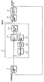
図1に前記の課題を解決するための本発明の位相同期回路の構成を示す。   FIG. 1 shows a configuration of a phase synchronization circuit of the present invention for solving the above-described problems.

この図において、2つの信号の位相差を検出し出力する位相検出回路11と、その位相検出回路11の出力を入力してフィルタリングをするフィルタ回路12と、そのフィルタ回路12の出力に固定値を加算する第2加算回路13と、この第2加算回路13の出力に応じた周波数の信号を出力する発振回路(VCO)14からなることは前記の従来のものと同じであるが、フィルタ12の内部構成が異なる。   In this figure, a phase detection circuit 11 that detects and outputs a phase difference between two signals, a filter circuit 12 that inputs and filters the output of the phase detection circuit 11, and a fixed value for the output of the filter circuit 12 The second adder circuit 13 for adding and the oscillation circuit (VCO) 14 for outputting a signal having a frequency corresponding to the output of the second adder circuit 13 are the same as those of the conventional one described above. The internal configuration is different.

フィルタ回路12の構成も図1中に示す。これは、前記位相検出回路11の出力に、第1のゲインをかける第1ゲイン回路121と、前記位相検出回路11の出力に第2のゲインをかける第2ゲイン回路122と、第2ゲイン回路122の出力を積分する積分回路123と、この積分回路123の積分値の上下限を決めるリミット回路124と、このリミット回路124の出力に第3のゲインをかける第3ゲイン回路125と、この第3ゲイン回路125の出力と前記第1ゲイン回路121の出力を加算する第1加算回路126で構成されている。積分回路123の前に第2ゲイン回路122を設けた点が、前記の従来のフィルタ構成と異なる。   The configuration of the filter circuit 12 is also shown in FIG. This includes a first gain circuit 121 that applies a first gain to the output of the phase detection circuit 11, a second gain circuit 122 that applies a second gain to the output of the phase detection circuit 11, and a second gain circuit. An integration circuit 123 for integrating the output of 122, a limit circuit 124 for determining upper and lower limits of the integration value of the integration circuit 123, a third gain circuit 125 for applying a third gain to the output of the limit circuit 124, The first adder circuit 126 is configured to add the output of the three gain circuit 125 and the output of the first gain circuit 121. The point that the second gain circuit 122 is provided before the integrating circuit 123 is different from the conventional filter configuration described above.

この点について説明する。   This point will be described.

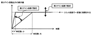
一般的に、積分回路の出力値に制限が無く大きさを無限にすることが出来るならば、積分回路の前後にゲイン回路を配置することは、積分回路の前のみ、又は後ろのみにゲインを配置することと理論的に等価になる。しかし、現実の回路では各回路の出力値は有限であり、特に積分回路では図1に示すように、リミット回路124のような値を制限するものが必要になる。そこで、第2ゲイン回路122により、積分回路123での積分値がリミット値になるまでの時定数を小さくし、この積分値が位相制御ループへ及ぼす影響は、第2ゲイン回路125で決める。これを図6で説明する。図6は第3ゲイン回路125の出力の絶対値の変化をイメージしたものである。図1の第2ゲイン回路122に一定の値が入力された時、時間と共に積分値が大きくなっていき、リミット回路124で制限される値で一定となる。ここで、積分値がリミット値に至るまでの時定数は第2ゲイン回路122のゲインにより決まる。位相制御ループへ及ぼす影響の最大値は、第3ゲイン回路125で決められるので、第2ゲイン回路122の値を増減しても位相制御ループへ及ぼす影響の最大値が変わることはない。   In general, if there is no limit on the output value of the integration circuit and the size can be made infinite, placing a gain circuit before and after the integration circuit will increase the gain only before or after the integration circuit. It is theoretically equivalent to placement. However, in an actual circuit, the output value of each circuit is finite, and in particular, in an integration circuit, as shown in FIG. Therefore, the second gain circuit 122 reduces the time constant until the integrated value in the integrating circuit 123 reaches the limit value, and the influence of the integrated value on the phase control loop is determined by the second gain circuit 125. This will be described with reference to FIG. FIG. 6 illustrates the change in the absolute value of the output of the third gain circuit 125. When a constant value is input to the second gain circuit 122 of FIG. 1, the integral value increases with time, and becomes constant at a value limited by the limit circuit 124. Here, the time constant until the integral value reaches the limit value is determined by the gain of the second gain circuit 122. Since the maximum value of the influence on the phase control loop is determined by the third gain circuit 125, even if the value of the second gain circuit 122 is increased or decreased, the maximum value of the influence on the phase control loop does not change.

以上のように、第1ゲイン回路121、第3ゲイン回路125は位相同期ループの定常時の安定性を優先する設定のままで、第2ゲイン回路122により外部基準信号と発振回路(VCO)14との位相が一致するまでの時間を短縮することができるようにしたものである。更に、第2ゲイン回路122のゲイン値を外部で設定出来るようにした第2ゲイン設定回路127により、この位相制御の速度を安定性を保持したまま希望する値に任意に設定出来るようにしたものである。   As described above, the first gain circuit 121 and the third gain circuit 125 remain set so as to give priority to the stability of the phase-locked loop in a steady state, and the second gain circuit 122 causes the external reference signal and the oscillation circuit (VCO) 14 to be set. The time until the phases coincide with each other can be shortened. Further, the second gain setting circuit 127 that allows the gain value of the second gain circuit 122 to be set externally can arbitrarily set the phase control speed to a desired value while maintaining stability. It is.

以上説明したように、本発明の位相同期回路は、図1で示した構成を有し、第1ゲイン回路121、第3ゲイン回路125は位相同期ループ本来の基本特性を満足するようにする設定とし、新たに加えた第2ゲイン回路122により、外部基準信号と発振回路(VCO)14との位相が一致するまでの時間を短縮することができるという効果がある。また、第2ゲイン回路122のゲイン値を外部で設定出来るようにした第2ゲイン設定回路127を設けたことで、安定性を保持したまま位相制御の速度を希望する値にすることが出来るという効果がある。例えば、前記の複合映像信号の色復調回路に使用した場合、安定性を保持したまま色位相が正規になるまでの時間を小さくできるという効果がある。   As described above, the phase locked loop of the present invention has the configuration shown in FIG. 1, and the first gain circuit 121 and the third gain circuit 125 are set so as to satisfy the basic characteristics inherent in the phase locked loop. Thus, the newly added second gain circuit 122 has an effect of shortening the time until the phase of the external reference signal and the oscillation circuit (VCO) 14 coincide. Further, by providing the second gain setting circuit 127 that allows the gain value of the second gain circuit 122 to be set externally, the phase control speed can be set to a desired value while maintaining stability. effective. For example, when used in the color demodulation circuit of the composite video signal, there is an effect that the time until the color phase becomes normal can be reduced while maintaining the stability.

また、外部から前記の第2ゲインを設定出来るため、色位相が正規になるまでの時間を必要に応じて任意に設定することが出来る。例えば信号中の色副搬送の振幅が安定しているVTR等の複合映像信号や強電界で受信したTV信号などの場合は、位相制御は可能な限り速い方がよいと思われる。しかし、車載用TV等で弱電界で受信したTV信号などの場合は、色副搬送波の位相が変化したかのように受信されることが考えられる。この場合位相制御を逆に遅くすることで色位相が誤って変化するのを緩和できるという効果が考えられる。   Further, since the second gain can be set from the outside, the time until the color phase becomes normal can be arbitrarily set as necessary. For example, in the case of a composite video signal such as a VTR in which the amplitude of the color sub-carrier in the signal is stable, or a TV signal received with a strong electric field, the phase control seems to be as fast as possible. However, in the case of a TV signal received with a weak electric field by a vehicle-mounted TV or the like, it may be received as if the phase of the color subcarrier has changed. In this case, it is conceivable that the color phase can be prevented from being erroneously changed by slowing down the phase control.

特に本発明の位相同期回路では、新たに設けた第2ゲイン回路122を第2ゲイン設定回路を通じて外部から設定することで、安定性を損なうことなく位相制御の速度のみを制御できるので、従来とは違った安定な制御が出来るという効果がある。   In particular, in the phase synchronization circuit of the present invention, by setting the newly provided second gain circuit 122 from the outside through the second gain setting circuit, it is possible to control only the speed of phase control without impairing stability. Has the effect of different and stable control.

以下、本発明の実施の形態を、図面を参照しながら説明する。   Hereinafter, embodiments of the present invention will be described with reference to the drawings.

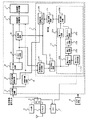
デジタル回路で実現する、前記した複合映像信号の色復調回路におけるバーストロック回路に本システムを適用した場合の実施例を図2に示す。   FIG. 2 shows an embodiment in which the present system is applied to a burst lock circuit in a color demodulation circuit for a composite video signal realized by a digital circuit.

TVチューナ2、又はVTR等の映像再生機器3からのアナログ複合映像信号は切り替え器4で選択されて、クロック回路20の任意のクロック周波数でAD変換器21によりデジタル信号に変換される。次にこの信号は2つに分けられ、一つはサンプル周波数変換回路22に入り、バーストロック回路27の中にある発振回路(デジタルVCO)275の出力周波数でサンプルされた信号に変換される。そしてもう一つは同期分離回路23に入り、複合映像信号中から水平同期信号と垂直同期信号を抽出する。水平同期信号と垂直同期信号はこの後の色搬送波検出回路271と映像信号処理回路28に入る。サンプル周波数変換回路22で変換された複合映像信号は、YC分離回路24で輝度信号と色信号に分離される。また、同時に輝度信号はこの後、映像信号処理回路28に入る。色信号はその振幅を制御するACC回路25を通り、色復調回路26で2つの色差信号に復調される。この復調のためにバーストロック回路27の中にある発振回路(デジタルVCO)275の出力を使用する。また、復調された2つの色差信号はこの後、映像信号処理回路28に入る。輝度信号と2つの色差信号は、映像信号処理回路28で適当な処理がなされ、映像信号表示装置29で表示される。一方、ACC回路25から出力される色信号はバーストロック回路27にも入る。ここに入った色信号は、まず色副搬送波検出回路271で色信号中の色副搬送波を抜き出し、発振回路(デジタルVCO)275の出力と共に位相検出回路272に入り、2つの信号の位相差を検出する。この検出された位相差出力は次にフィルタ回路273に入る。ここに入った位相差出力は、まず1つは第1ゲイン回路2731に入る。もう一つは第2ゲイン回路2732に入る。その出力は積分回路2733に入り、その出力はリミット回路2734に入る。そしてその出力は第3ゲイン回路2735に入る。次に前記の第1ゲイン回路2731の出力と第3ゲイン回路2735の出力は第1加算回路2736で加算される。そしてこの加算された結果に、発振回路(デジタルVCO回路)275の出力周波数の中心値を決める固定値を第2加算回路274で加算する。そしてこの加算結果を発振回路(デジタルVCO回路)275に入力する。発振回路(デジタルVCO)275は、色副搬送波周波数に相当する周波数の信号とその4倍または8倍に相当する周波数の信号とサンプル周波数変換回路22を制御するための信号を出力する。色搬送波周波数に相当する周波数の信号は、前記位相検出回路272と色復調回路26に入る。色副搬送波周波数の4倍または8倍の周波数に相当する信号とサンプル周波数変換回路22を制御するための信号は、サンプル周波数変換回路22に入る。   The analog composite video signal from the TV tuner 2 or the video reproduction device 3 such as a VTR is selected by the switch 4 and converted into a digital signal by the AD converter 21 at an arbitrary clock frequency of the clock circuit 20. Next, this signal is divided into two, and one enters the sample frequency conversion circuit 22 and is converted into a signal sampled at the output frequency of the oscillation circuit (digital VCO) 275 in the burst lock circuit 27. The other enters the sync separation circuit 23 and extracts a horizontal sync signal and a vertical sync signal from the composite video signal. The horizontal synchronization signal and the vertical synchronization signal enter the color carrier wave detection circuit 271 and the video signal processing circuit 28 thereafter. The composite video signal converted by the sample frequency conversion circuit 22 is separated into a luminance signal and a color signal by the YC separation circuit 24. At the same time, the luminance signal then enters the video signal processing circuit 28. The color signal passes through an ACC circuit 25 that controls its amplitude, and is demodulated into two color difference signals by a color demodulation circuit 26. For this demodulation, the output of the oscillation circuit (digital VCO) 275 in the burst lock circuit 27 is used. Further, the demodulated two color difference signals thereafter enter the video signal processing circuit 28. The luminance signal and the two color difference signals are appropriately processed by the video signal processing circuit 28 and displayed on the video signal display device 29. On the other hand, the color signal output from the ACC circuit 25 also enters the burst lock circuit 27. First, the color subcarrier detection circuit 271 extracts the color subcarrier from the color signal, and enters the phase detection circuit 272 together with the output of the oscillation circuit (digital VCO) 275 to determine the phase difference between the two signals. To detect. This detected phase difference output then enters the filter circuit 273. One of the phase difference outputs entered here first enters the first gain circuit 2731. The other enters the second gain circuit 2732. The output enters the integration circuit 2733 and the output enters the limit circuit 2734. The output then enters the third gain circuit 2735. Next, the output of the first gain circuit 2731 and the output of the third gain circuit 2735 are added by a first addition circuit 2736. Then, a fixed value that determines the center value of the output frequency of the oscillation circuit (digital VCO circuit) 275 is added to the addition result by the second addition circuit 274. Then, the addition result is input to an oscillation circuit (digital VCO circuit) 275. The oscillation circuit (digital VCO) 275 outputs a signal having a frequency corresponding to the color subcarrier frequency, a signal having a frequency corresponding to four times or eight times thereof, and a signal for controlling the sample frequency conversion circuit 22. A signal having a frequency corresponding to the color carrier frequency enters the phase detection circuit 272 and the color demodulation circuit 26. A signal corresponding to a frequency four or eight times the color subcarrier frequency and a signal for controlling the sample frequency conversion circuit 22 enter the sample frequency conversion circuit 22.

また、TVチューナ2で受信した受信状態を判別する信号と、複合映像信号がTVチューナ2のものかVTR等の映像再生機器3のものかを判断する信号を切り替え器4からCPU1に取り込み、CPU1から第2ゲイン設定回路2737を制御する。   In addition, a signal for determining the reception state received by the TV tuner 2 and a signal for determining whether the composite video signal is for the TV tuner 2 or the video reproduction device 3 such as a VTR are taken into the CPU 1 from the switch 4 and the CPU 1 The second gain setting circuit 2737 is controlled.

次に動作を説明する。   Next, the operation will be described.

AD変換回路21でデジタル値に変換されたアナログの複合映像信号は、サンプル周波数変換回路22でクロック回路20の周波数でサンプルされた複合映像信号を、バーストロック回路27の出力信号周波数でサンプルされた信号に変換する。この周波数は後で述べるように最終的に複合映像信号の色副搬送周波数の4倍または8倍の周波数になる。サンプル周波数変換回路22の出力は、YC分離回路24で輝度信号と色信号に分離される。輝度信号の方はそのまま後の映像信号処理回路28に入る。色信号の方はACC回路25を通って、色復調回路26に入る。色復調回路26はバーストロック回路27の出力信号を用いて2つの色差信号に復調する。このバーストロック回路27からの信号は後で述べるように、最終的に複合映像信号の色副搬送に周波数と位相が一致した信号になる。復調された2つの色差信号は後の映像信号処理回路28に入り、前記の輝度信号と共に後段の映像信号表示装置29に適した信号に変換される。ACC回路25を通った色信号は、色復調回路26とは別にバーストロック回路27にも入る。ここではまず、同期分離回路23で抽出された水平同期信号と垂直同期信号を用いて色信号から色副搬送波を抽出する。これが色副搬送波検出回路271である。ここで抽出された色副搬送波は、位相検出回路272で、発振回路(デジタルVCO回路)275から出力される色副搬送周波数相当の信号との位相差を検出する。ここで検出された位相誤差はフィルタ回路273を通り、第2加算回路274で適当な固定値を加算して発振回路(デジタルVCO回路)275を制御する。発振回路(デジタルVCO回路)275からは、色副搬送波の4倍または8倍に相当する信号も出力されており、これはサンプル周波数変換回路22に入力されて、映像信号を色搬送波の4倍または8倍に相当する周波数のサンプル信号に変換している。ここで、バーストロック回路27で色副搬送波信号に対する位相同期ループが形成されており、最終的に位相同期状態になった時、発振回路(デジタルVCO回路)275からは、入力された映像信号中の色副搬送波と周波数及び位相の一致した信号と、その4倍または8倍の周波数の信号が出力される。色復調回路26と位相検出回路272は、この前者の信号を用いているので、位相同期状態になることで正規の色復調が行なえる。   The analog composite video signal converted into a digital value by the AD conversion circuit 21 is sampled at the output signal frequency of the burst lock circuit 27 from the composite video signal sampled at the frequency of the clock circuit 20 by the sample frequency conversion circuit 22. Convert to signal. As will be described later, this frequency finally becomes 4 or 8 times the color subcarrier frequency of the composite video signal. The output of the sample frequency conversion circuit 22 is separated into a luminance signal and a color signal by the YC separation circuit 24. The luminance signal enters the subsequent video signal processing circuit 28 as it is. The color signal enters the color demodulation circuit 26 through the ACC circuit 25. The color demodulation circuit 26 demodulates the two color difference signals using the output signal of the burst lock circuit 27. As will be described later, the signal from the burst lock circuit 27 finally becomes a signal having the same frequency and phase as the color subcarrier of the composite video signal. The demodulated two color difference signals enter the subsequent video signal processing circuit 28 and are converted into a signal suitable for the subsequent video signal display device 29 together with the luminance signal. The color signal that has passed through the ACC circuit 25 also enters the burst lock circuit 27 separately from the color demodulation circuit 26. Here, first, the color subcarrier is extracted from the color signal using the horizontal synchronization signal and the vertical synchronization signal extracted by the synchronization separation circuit 23. This is the color subcarrier detection circuit 271. The phase detection circuit 272 detects the phase difference of the color subcarrier extracted here from the signal corresponding to the color subcarrier frequency output from the oscillation circuit (digital VCO circuit) 275. The detected phase error passes through the filter circuit 273, and an appropriate fixed value is added by the second addition circuit 274 to control the oscillation circuit (digital VCO circuit) 275. The oscillation circuit (digital VCO circuit) 275 also outputs a signal corresponding to 4 or 8 times the color subcarrier, which is input to the sample frequency conversion circuit 22 to convert the video signal to 4 times the color carrier. Alternatively, it is converted into a sample signal having a frequency corresponding to eight times. Here, the phase lock loop for the color subcarrier signal is formed in the burst lock circuit 27, and when the phase lock state is finally reached, the oscillation circuit (digital VCO circuit) 275 receives from the input video signal. A signal having the same frequency and phase as that of the color subcarrier and a signal having a frequency that is four times or eight times that of the color subcarrier is output. Since the color demodulation circuit 26 and the phase detection circuit 272 use the former signal, normal color demodulation can be performed by entering the phase synchronization state.

ここで、入力した複合映像信号中の色副搬送波の周波数が基準値とずれていた場合、フィルタ回路273の作用により、発振回路(デジタルVCO)275の出力周波数・位相は入力された映像信号の色副搬送波に一致するように動作する。ここで、第2ゲイン設定回路2737で設定された値に基づいた第2ゲイン回路2732の働きで、希望する速度で位相同期を行わせることが出来、その結果、希望する速度で色位相を合わせることが出来る。   Here, when the frequency of the color subcarrier in the input composite video signal deviates from the reference value, the output frequency / phase of the oscillation circuit (digital VCO) 275 is changed by the action of the filter circuit 273. Operates to match the color subcarrier. Here, the phase of the phase can be synchronized at a desired speed by the action of the second gain circuit 2732 based on the value set by the second gain setting circuit 2737. As a result, the color phase is adjusted at the desired speed. I can do it.

更に、CPU1により入力複合映像信号の種類を判定し、入力した複合映像信号がVTR等の映像再生機器3からのものである時は、位相制御が速くなるように第2ゲイン設定回路2737を制御する信号をCPU1から出力することで、高速に位相同期を行わせることが出来る。また、入力した複合映像信号がTVチューナ2からのものである時は、受信状態が強電界であるか弱電界であるかをCPU1で判定し、強電界である時は位相制御が速くなるように、弱電界である時は位相制御が遅くなるように第2ゲイン設定回路を制御する信号をCPU1から出力することで、安定性を保持したまま強電界時は高速に色同期を行わせ、弱電界時は色同期の誤動作を緩和することが出来る。   Further, the type of the input composite video signal is determined by the CPU 1, and when the input composite video signal is from the video reproduction device 3 such as a VTR, the second gain setting circuit 2737 is controlled so that the phase control becomes faster. By outputting a signal to be output from the CPU 1, phase synchronization can be performed at high speed. When the input composite video signal is from the TV tuner 2, the CPU 1 determines whether the reception state is a strong electric field or a weak electric field, and when it is a strong electric field, the phase control becomes faster. In addition, by outputting a signal for controlling the second gain setting circuit from the CPU 1 so that the phase control is delayed when the electric field is weak, color synchronization is performed at high speed when the electric field is strong while maintaining stability. When the electric field is weak, malfunction of color synchronization can be alleviated.

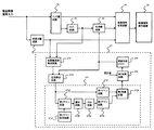
前記した複合映像信号の色復調をアナログ回路で実現したバーストロック回路に本システムを適用した場合の実施例を図3に示す。   FIG. 3 shows an embodiment in which the present system is applied to a burst lock circuit in which the color demodulation of the composite video signal described above is realized by an analog circuit.

アナログの複合映像信号を入力する。この信号は2つに分けられ、1つはYC分離回路34に入り、輝度信号と色差信号に分離される。そしてもう一つは同期分離回路33に入り、複合映像信号中から水平同期信号と垂直同期信号を抽出する。水平同期信号と垂直同期信号はこの後の色副搬送波検出回路371と映像信号処理回路38に入る。YC分離回路34で分離された輝度信号はこの後、映像信号処理回路38に入る。同じくYC分離回路34で分離された色信号はその振幅を一定にするACC回路35を通り、色復調回路36で2つの色差信号に復調される。この復調のためにバーストロック回路37中の発振回路375の出力を使用する。また、復調された2つの色差信号はこの後、映像信号処理回路38に入る。輝度信号と2つの色差信号は、映像信号処理回路38で適当な処理がなされ、映像信号表示装置39で表示される。一方、ACC回路35から出力される色信号はバーストロック回路37に入る。ここに入った色信号はまず、色副搬送波検出回路371で色信号中の色副搬送波を抜き出し、発振回路(VCO)375の出力と共に位相検出回路372に入り、2つの信号の位相差を検出する。この検出された位相差出力は次にフィルタ回路373に入る。ここに入った位相差出力は、まず1つは第1ゲイン回路3731に入る。もう一つは第2ゲイン回路3732に入る。その出力は積分回路3733に入り、その出力はリミット回路3734に入る。そしてその出力は第3ゲイン回路3735に入る。次に前記の第1ゲイン回路3731の出力と第3ゲイン回路3735の出力は第1加算回路3736で加算される。そしてこの加算された結果に、発振回路(VCO)375の出力周波数の中心値を決める固定量を第2加算回路374で加算する。そしてこの加算結果を発振回路(VCO)375に入力する。発振回路(VCO)375は、色副搬送波に相当する周波数の信号を出力する。   Input an analog composite video signal. This signal is divided into two, and one enters the YC separation circuit 34 and is separated into a luminance signal and a color difference signal. The other enters the sync separation circuit 33 and extracts a horizontal sync signal and a vertical sync signal from the composite video signal. The horizontal synchronization signal and the vertical synchronization signal enter the color subcarrier detection circuit 371 and the video signal processing circuit 38 thereafter. The luminance signal separated by the YC separation circuit 34 then enters the video signal processing circuit 38. Similarly, the color signal separated by the YC separation circuit 34 passes through the ACC circuit 35 for making the amplitude constant, and is demodulated into two color difference signals by the color demodulation circuit 36. For this demodulation, the output of the oscillation circuit 375 in the burst lock circuit 37 is used. The two demodulated color difference signals then enter the video signal processing circuit 38. The luminance signal and the two color difference signals are appropriately processed by the video signal processing circuit 38 and displayed on the video signal display device 39. On the other hand, the color signal output from the ACC circuit 35 enters the burst lock circuit 37. First, the color subcarrier detection circuit 371 extracts the color subcarrier from the color signal, and enters the phase detection circuit 372 together with the output of the oscillation circuit (VCO) 375 to detect the phase difference between the two signals. To do. This detected phase difference output then enters the filter circuit 373. One of the phase difference outputs entered here first enters the first gain circuit 3731. The other enters the second gain circuit 3732. The output enters the integration circuit 3733 and the output enters the limit circuit 3734. The output then enters the third gain circuit 3735. Next, the output of the first gain circuit 3731 and the output of the third gain circuit 3735 are added by a first addition circuit 3736. Then, a fixed amount that determines the center value of the output frequency of the oscillation circuit (VCO) 375 is added to the result of the addition by the second addition circuit 374. Then, the addition result is input to an oscillation circuit (VCO) 375. The oscillation circuit (VCO) 375 outputs a signal having a frequency corresponding to the color subcarrier.

次に動作を説明する。   Next, the operation will be described.

アナログの複合映像信号は、YC分離回路34で輝度信号と色信号に分離される。輝度信号の方はそのまま後の映像信号処理回路38に入る。色信号の方はACC回路35を通って、色復調回路36に入る。色復調回路36はバーストロック回路37の中の発振回路(VCO)375の出力信号を用いて、入力された色信号を2つの色差信号に復調する。この発振回路(VCO)375の出力信号は後で述べるようにバーストロック回路37の働きで最終的に複合映像信号の色副搬送波に周波数と位相が一致した信号になる。復調された2つの色差信号は後の映像信号処理回路38に入り、前記の輝度信号と共に後段の映像信号表示装置39に適した信号に変換される。ACC回路35を通った色信号は、色復調回路36とは別にバーストロック回路37にも入る。ここではまず、同期分離回路33で抽出された水平同期信号と垂直同期信号を用いて色信号から色副搬送波を抽出する。これが色副搬送波検出回路371である。ここで抽出された色副搬送波は、位相検出回路372で、発振回路(VCO)375から出力される色副搬送周波数相当の信号との位相差を検出する。ここで検出された位相誤差はフィルタ回路373を通り、第2加算回路374で適当な固定量を加算して発振回路(VCO)375を制御する。ここで、バーストロック回路37で色副搬送信号に対する位相同期ループが形成されており、最終的に位相同期状態になった時、発振回路(VCO)375からは、入力された映像信号中の色副搬送波と周波数及び位相の一致した信号が出力される。色復調回路36はこの信号を用いているので、位相同期状態になることで正規の色復調が行なえる。   The analog composite video signal is separated into a luminance signal and a color signal by the YC separation circuit 34. The luminance signal enters the subsequent video signal processing circuit 38 as it is. The color signal enters the color demodulation circuit 36 through the ACC circuit 35. The color demodulation circuit 36 demodulates the input color signal into two color difference signals using the output signal of the oscillation circuit (VCO) 375 in the burst lock circuit 37. The output signal of the oscillation circuit (VCO) 375 finally becomes a signal whose frequency and phase coincide with the color subcarrier of the composite video signal by the action of the burst lock circuit 37 as described later. The demodulated two color difference signals enter the subsequent video signal processing circuit 38 and are converted into a signal suitable for the subsequent video signal display device 39 together with the luminance signal. The color signal that has passed through the ACC circuit 35 also enters the burst lock circuit 37 in addition to the color demodulation circuit 36. Here, first, the color subcarrier is extracted from the color signal using the horizontal synchronization signal and the vertical synchronization signal extracted by the synchronization separation circuit 33. This is the color subcarrier detection circuit 371. The phase detection circuit 372 detects the phase difference of the color subcarrier extracted here from the signal corresponding to the color subcarrier frequency output from the oscillation circuit (VCO) 375. The detected phase error passes through the filter circuit 373, and an appropriate fixed amount is added by the second addition circuit 374 to control the oscillation circuit (VCO) 375. Here, the phase lock loop for the color subcarrier signal is formed in the burst lock circuit 37, and when the phase lock state is finally reached, the oscillation circuit (VCO) 375 outputs the color in the input video signal. A signal having the same frequency and phase as the subcarrier is output. Since the color demodulation circuit 36 uses this signal, normal color demodulation can be performed when the phase is synchronized.

ここで、入力した複合映像信号中の色副搬送波の周波数・位相が基準値とずれていた場合、フィルタ回路373の作用により、発振回路(VCO)375の出力周波数・位相は入力された映像信号の色副搬送波に一致するように動作する。ここで、第2ゲイン設定回路3737で設定された値に基づいた第2ゲイン回路3732の働きで、希望する速度で位相同期を行わせることが出来、その結果、希望する速度で色位相を合わせることが出来る。   Here, when the frequency / phase of the color subcarrier in the input composite video signal deviates from the reference value, the output frequency / phase of the oscillation circuit (VCO) 375 is input by the action of the filter circuit 373. To match the color subcarrier of the. Here, the operation of the second gain circuit 3732 based on the value set by the second gain setting circuit 3737 allows phase synchronization to be performed at a desired speed, and as a result, the color phase is adjusted at the desired speed. I can do it.

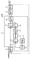
本システムにおいて、位相検出回路から出力される誤差の値に応じて第2ゲイン回路のゲインを変えるようにした場合の実施例を図5に示す。   FIG. 5 shows an embodiment in which the gain of the second gain circuit is changed in accordance with the error value output from the phase detection circuit in this system.

2つの信号の位相差を検出し出力する位相検出回路51と、その位相検出回路51の出力を入力してフィルタリングをするフィルタ回路52と、そのフィルタ回路52の出力に固定値を加算する第2加算回路53と、この第2加算回路53の出力に応じた周波数の信号を出力する発振回路(VCO)54からなる。   A phase detection circuit 51 that detects and outputs a phase difference between two signals, a filter circuit 52 that receives and filters the output of the phase detection circuit 51, and a second that adds a fixed value to the output of the filter circuit 52 The circuit includes an adder circuit 53 and an oscillation circuit (VCO) 54 that outputs a signal having a frequency corresponding to the output of the second adder circuit 53.

更にフィルタ52の内部構成を図5中に示す。前記位相検出回路51の出力に、第1のゲインをかける第1ゲイン回路521と、前記位相検出回路51の出力に第2のゲインをかける第2ゲイン回路522と、第2ゲイン回路522の出力を積分する積分回路523と、この積分回路523の積分値の上下限を決めるリミット回路524と、このリミット回路の出力に第3のゲインをかける第3ゲイン回路525と、この第3ゲイン回路525の出力と前記第1ゲイン回路521の出力を加算する第1加算器526で構成されている。更に第3ゲイン設定回路527と、位相検出回路51の出力レベルを判定する判定回路528とを備え、判定回路528の出力で第2ゲイン設定回路527を制御し、この結果に基づき第2ゲイン回路522でゲインをかける構成になっている。   Furthermore, the internal structure of the filter 52 is shown in FIG. A first gain circuit 521 that applies a first gain to the output of the phase detection circuit 51, a second gain circuit 522 that applies a second gain to the output of the phase detection circuit 51, and an output of the second gain circuit 522 Integrating circuit 523, limit circuit 524 for determining the upper and lower limits of the integration value of this integrating circuit 523, third gain circuit 525 for applying a third gain to the output of this limit circuit, and this third gain circuit 525 And the output of the first gain circuit 521 are added to a first adder 526. Further, a third gain setting circuit 527 and a determination circuit 528 for determining the output level of the phase detection circuit 51 are provided. The second gain setting circuit 527 is controlled by the output of the determination circuit 528, and the second gain circuit is based on the result. At 522, a gain is applied.

次に動作を説明する。   Next, the operation will be described.

入力された外部基準信号は、位相検出回路51で発振回路(VCO)54から出力される信号との位相差を検出する。ここで検出された位相誤差はフィルタ回路52を通り、第2加算回路53で適当な固定値を加算して発振回路(VCO)54を制御する。ここで、外部基準信号に対する位相同期ループが形成されており、第2ゲイン設定回路527で設定された値に基づいた第2ゲイン回路522の働きで、希望する速度で位相同期を行わせることが出来、その結果希望する速度で色位相を合わせることが出来る。   The input external reference signal detects a phase difference from the signal output from the oscillation circuit (VCO) 54 by the phase detection circuit 51. The phase error detected here passes through the filter circuit 52, and an appropriate fixed value is added by the second addition circuit 53 to control the oscillation circuit (VCO) 54. Here, a phase-locked loop for the external reference signal is formed, and phase synchronization can be performed at a desired speed by the action of the second gain circuit 522 based on the value set by the second gain setting circuit 527. As a result, the color phase can be adjusted at a desired speed.

ここで、判定回路528で位相検出回路51の出力レベルを判定して、判定結果に基づき第2ゲイン設定回路527の設定値を制御する。これにより、位相誤差が大きい時には、第2ゲイン回路522のゲイン値を大きくして位相同期を加速し、位相誤差がある程度小さくなると位相同期を加速する必要なしと判断して、第2ゲイン回路522のゲイン値を小さくして、位相同期ループをより安定にさせることが出来る。   Here, the output level of the phase detection circuit 51 is determined by the determination circuit 528, and the set value of the second gain setting circuit 527 is controlled based on the determination result. Thus, when the phase error is large, the gain value of the second gain circuit 522 is increased to accelerate the phase synchronization, and when the phase error becomes small to some extent, it is determined that it is not necessary to accelerate the phase synchronization, and the second gain circuit 522 The gain value can be reduced to make the phase locked loop more stable.

本発明に係る位相同期回路は、位相同期ループの安定性を保持したまま位相制御の速度を制御できるという効果を有し、外部基準信号に位相同期した信号をつくり出す位相同期回路として有用である。   The phase-locked loop according to the present invention has an effect that the speed of phase control can be controlled while maintaining the stability of the phase-locked loop, and is useful as a phase-locked loop that generates a signal that is phase-locked with an external reference signal.

本発明の位相同期回路の構成を示すブロック図The block diagram which shows the structure of the phase-locked loop circuit of this invention 本発明の実施例1の構成を示すブロック図The block diagram which shows the structure of Example 1 of this invention. 本発明の実施例2の構成を示すブロック図The block diagram which shows the structure of Example 2 of this invention. 従来例の位相同期回路の構成を示すブロック図Block diagram showing the configuration of a conventional phase synchronization circuit 本発明の実施例3の構成を示すブロック図The block diagram which shows the structure of Example 3 of this invention. 本発明の動作を説明するための図The figure for demonstrating operation | movement of this invention

符号の説明Explanation of symbols

1 マイクロコンピュータ
2 TVチューナ
3 複合映像信号を出力するVTR等の映像再生機器
4 切り替え器
11、272、372、41、51 位相検出回路
12、273、373、42、52 フィルタ回路
121、2731、3731、421、521 第1ゲイン回路
122、2732、3732、425、522 第2ゲイン回路
123、2733、3733、423、523 積分回路
124、2734、3734、424、524 リミット回路
125、2735、3735、525 第3ゲイン回路
126、2736、3736、426、526 第1加算回路
528 判定回路
127、2737、3737、527 第2ゲイン設定回路
13、274、374、43、53 第2加算回路
14、375、44、54 発振回路(VCO)
275 発振回路(デジタルVCO)
20 クロック回路
21 AD変換回路
22 サンプル周波数変換回路
23、33 同期分離回路
24、34 YC分離回路
25、35 ACC回路
26、36 色復調回路
27、37 バーストロック回路
271、371 色副搬送波検出回路
28、38 映像信号処理回路
29、39 映像信号表示装置
DESCRIPTION OF SYMBOLS 1 Microcomputer 2 TV tuner 3 Video reproduction apparatuses, such as VTR which outputs a composite video signal 4, Switch 11,272,372,41,51 Phase detection circuit 12,273,373,42,52 Filter circuit 121,2731,3731 , 421, 521 First gain circuit 122, 2732, 3732, 425, 522 Second gain circuit 123, 2733, 3733, 423, 523 Integration circuit 124, 2734, 3734, 424, 524 Limit circuit 125, 2735, 3735, 525 Third gain circuit 126, 2736, 3736, 426, 526 First addition circuit 528 Determination circuit 127, 2737, 3737, 527 Second gain setting circuit 13, 274, 374, 43, 53 Second addition circuit 14, 375, 44 54 Oscillator (V CO)
275 Oscillator (Digital VCO)
20 Clock circuit 21 AD conversion circuit 22 Sample frequency conversion circuit 23, 33 Sync separation circuit 24, 34 YC separation circuit 25, 35 ACC circuit 26, 36 Color demodulation circuit 27, 37 Burst lock circuit 271, 371 Color subcarrier detection circuit 28 , 38 Video signal processing circuit 29, 39 Video signal display device

Claims (6)

外部信号に位相同期した信号を作り出す位相同期システムにおける定常的な位相偏差であるオフセットを無くするための位相同期回路であって、外部から入力した信号の位相を検出する位相検出回路と、位相検出回路からの出力にゲインをかける第1ゲイン回路と、位相検出回路からの出力にゲインをかけるもう一つのゲイン回路である第2ゲイン回路と、第2ゲイン回路の出力を積分する積分回路と、積分回路の出力をある一定値で制限するリミット回路と、リミット回路の出力にゲインをかける第3ゲイン回路と、第1ゲイン回路の出力と第3ゲイン回路の出力を加算する第1加算回路と、第1加算回路からの出力にある固定値を加算する第2加算回路と、第2加算回路からの出力で決まる周波数の信号を出力する発振回路(VCO)とを備え、第1ゲイン回路及び、第3ゲイン回路で、位相同期ループが安定に動作するように設定し、第2ゲイン回路の設定で積分回路の収束を速めることにより、位相同期ループの安定を保持したまま高速な位相制御ができるようにしたことを特徴とする位相同期回路。 A phase synchronization circuit for eliminating an offset that is a steady phase deviation in a phase synchronization system that generates a signal that is phase-synchronized with an external signal, a phase detection circuit that detects the phase of an externally input signal, and a phase detection A first gain circuit that applies gain to the output from the circuit; a second gain circuit that is another gain circuit that applies gain to the output from the phase detection circuit; and an integration circuit that integrates the output of the second gain circuit; A limit circuit that limits the output of the integration circuit at a certain value; a third gain circuit that applies gain to the output of the limit circuit; and a first addition circuit that adds the output of the first gain circuit and the output of the third gain circuit; A second adder circuit that adds a fixed value in the output from the first adder circuit, and an oscillation circuit (VCO) that outputs a signal having a frequency determined by the output from the second adder circuit; The first and third gain circuits are set so that the phase-locked loop operates stably, and the stability of the phase-locked loop is maintained by accelerating the convergence of the integrating circuit by setting the second gain circuit. A phase synchronization circuit characterized in that high-speed phase control can be performed as it is. 前記位相同期回路において、積分器の前に配置した第2ゲイン回路にかける係数を外部から設定できる第2ゲイン設定回路を設けて、位相制御の速度を外部から任意に設定できるようにしたことを特徴とする請求項1に記載の位相同期回路。 In the phase-locked loop, a second gain setting circuit that can externally set a coefficient applied to the second gain circuit arranged in front of the integrator is provided so that the phase control speed can be arbitrarily set from the outside. The phase-locked loop according to claim 1. 前記位相同期回路のVCOからの出力を複合映像信号の色復調処理をするための搬送波に使用することを特徴とする請求項1及び2に記載の位相同期回路。 3. The phase synchronization circuit according to claim 1, wherein the output from the VCO of the phase synchronization circuit is used as a carrier wave for color demodulation processing of a composite video signal. 前記位相同期回路において、位相検出回路から出力される位相誤差の値に応じて第2ゲイン回路のゲインを変えるようにしたことを特徴とする請求項1及び2に記載の位相同期回路。 3. The phase synchronization circuit according to claim 1, wherein in the phase synchronization circuit, the gain of the second gain circuit is changed in accordance with the value of the phase error output from the phase detection circuit. 前記位相同期回路を用いた色復調回路において、入力した複合映像信号がTV信号である場合、受信波の電界強度に応じて第2ゲイン回路のゲインを変えるようにしたことで、安定性を保持したまま強電界での高速な色同期と弱電界での色同期の安定化が出来ることを特徴とする請求項1及び2に記載の位相同期回路。 In the color demodulation circuit using the phase synchronization circuit, when the input composite video signal is a TV signal, stability is maintained by changing the gain of the second gain circuit in accordance with the electric field strength of the received wave. 3. The phase locked loop according to claim 1, wherein high-speed color synchronization in a strong electric field and color synchronization in a weak electric field can be stabilized. 前記位相同期回路を用いた色復調回路において、入力した複合映像信号が、TV信号のような色副搬送波周波数が正確な信号である場合と、VTR信号等の色副搬送波周波数が正確でない可能性がある信号である場合とで、第2ゲイン回路のゲインを変えるようにしたことで、安定性を保持したまま高速な色同期が出来ることを特徴とする請求項1及び2に記載の位相同期回路。 In the color demodulation circuit using the phase synchronization circuit, the input composite video signal may be a signal with an accurate color subcarrier frequency such as a TV signal, and the color subcarrier frequency such as a VTR signal may not be accurate. 3. The phase synchronization according to claim 1, wherein high-speed color synchronization can be performed while maintaining stability by changing the gain of the second gain circuit when the signal is a certain signal. circuit.
JP2004103762A 2004-03-31 2004-03-31 Phase locking circuit Pending JP2005294981A (en)

Priority Applications (1)

Application Number Priority Date Filing Date Title
JP2004103762A JP2005294981A (en) 2004-03-31 2004-03-31 Phase locking circuit

Applications Claiming Priority (1)

Application Number Priority Date Filing Date Title
JP2004103762A JP2005294981A (en) 2004-03-31 2004-03-31 Phase locking circuit

Publications (1)

Publication Number Publication Date
JP2005294981A true JP2005294981A (en) 2005-10-20

Family

ID=35327468

Family Applications (1)

Application Number Title Priority Date Filing Date
JP2004103762A Pending JP2005294981A (en) 2004-03-31 2004-03-31 Phase locking circuit

Country Status (1)

Country Link
JP (1) JP2005294981A (en)

Cited By (1)

* Cited by examiner, † Cited by third party
Publication number Priority date Publication date Assignee Title
JP2009027581A (en) * 2007-07-23 2009-02-05 Renesas Technology Corp Semiconductor integrated circuit

Citations (11)

* Cited by examiner, † Cited by third party
Publication number Priority date Publication date Assignee Title
JPS62253224A (en) * 1986-01-14 1987-11-05 Toshiba Corp Phase synchronizing circuit
JPH02148985A (en) * 1988-06-02 1990-06-07 Philips Gloeilampenfab:Nv Video signal processing circuit
JPH04365267A (en) * 1991-06-13 1992-12-17 Mitsubishi Electric Corp Variable time constant type afc circuit
JPH05129946A (en) * 1991-11-08 1993-05-25 Sony Corp Pll circuit
JP2547563B2 (en) * 1986-03-28 1996-10-23 アールシーエー トムソン ライセンシング コーポレーシヨン Stabilizer
JPH0974499A (en) * 1995-06-13 1997-03-18 Texas Instr Inc <Ti> Signal processing method using tracking filter and filter
JPH10200400A (en) * 1997-01-13 1998-07-31 Hitachi Ltd Phase synchronizing circuit
JP2001168712A (en) * 1999-12-13 2001-06-22 Matsushita Electric Ind Co Ltd Clock extraction circuit
JP2002111491A (en) * 2000-09-27 2002-04-12 Ricoh Co Ltd Phase locked circuit
JP2002152041A (en) * 2000-11-08 2002-05-24 Nec Corp Feedback control circuit and pll circuit
JP3323824B2 (en) * 1999-02-22 2002-09-09 松下電器産業株式会社 Clock generation circuit

Patent Citations (11)

* Cited by examiner, † Cited by third party
Publication number Priority date Publication date Assignee Title
JPS62253224A (en) * 1986-01-14 1987-11-05 Toshiba Corp Phase synchronizing circuit
JP2547563B2 (en) * 1986-03-28 1996-10-23 アールシーエー トムソン ライセンシング コーポレーシヨン Stabilizer
JPH02148985A (en) * 1988-06-02 1990-06-07 Philips Gloeilampenfab:Nv Video signal processing circuit
JPH04365267A (en) * 1991-06-13 1992-12-17 Mitsubishi Electric Corp Variable time constant type afc circuit
JPH05129946A (en) * 1991-11-08 1993-05-25 Sony Corp Pll circuit
JPH0974499A (en) * 1995-06-13 1997-03-18 Texas Instr Inc <Ti> Signal processing method using tracking filter and filter
JPH10200400A (en) * 1997-01-13 1998-07-31 Hitachi Ltd Phase synchronizing circuit
JP3323824B2 (en) * 1999-02-22 2002-09-09 松下電器産業株式会社 Clock generation circuit
JP2001168712A (en) * 1999-12-13 2001-06-22 Matsushita Electric Ind Co Ltd Clock extraction circuit
JP2002111491A (en) * 2000-09-27 2002-04-12 Ricoh Co Ltd Phase locked circuit
JP2002152041A (en) * 2000-11-08 2002-05-24 Nec Corp Feedback control circuit and pll circuit

Cited By (1)

* Cited by examiner, † Cited by third party
Publication number Priority date Publication date Assignee Title
JP2009027581A (en) * 2007-07-23 2009-02-05 Renesas Technology Corp Semiconductor integrated circuit

Similar Documents

Publication Publication Date Title
US4933767A (en) Video intermediate frequency signal processing circuit
JPH09182100A (en) Pll circuit
JP2005294981A (en) Phase locking circuit
KR890004218B1 (en) Synchronizing picture signal detecting circuit
JP2007181046A (en) Receiving circuit, receiver and receiving method
US7634037B2 (en) Digital phase-locked loop circuit and a method thereof
JPH02180473A (en) Keyed synchronous detection circuit
JPH08125884A (en) Pll circuit
JPH0846433A (en) Video signal demodulating circuit
JPH11150735A (en) Signal generating circuit
JP2001156627A (en) Phase detector and phase detection method
JP3617918B2 (en) Automatic frequency tuning circuit
JPH0715216Y2 (en) PLL tuning device
JP2002010169A (en) Aft circuit
JP2006186548A (en) Phase synchronization circuit
JPH0486079A (en) Video processor
JP3171980B2 (en) Phase locked loop circuit
JP3249363B2 (en) Clock recovery circuit
JP2641290B2 (en) Clock generator
JPS5930388A (en) Multi-purpose color television receiver
JP2001169302A (en) Color signal processing circuit
JPH04192885A (en) Horizontal synchronizing circuit of television receiver
JPH04100412A (en) Phase locked loop circuit
JPH04189034A (en) Phase locked loop pick-up circuit in common use with afc loop
JPS61202503A (en) Synchronous detector using phase locked loop circuit

Legal Events

Date Code Title Description
A621 Written request for application examination

Free format text: JAPANESE INTERMEDIATE CODE: A621

Effective date: 20070116

RD01 Notification of change of attorney

Free format text: JAPANESE INTERMEDIATE CODE: A7421

Effective date: 20070214

RD01 Notification of change of attorney

Free format text: JAPANESE INTERMEDIATE CODE: A7421

Effective date: 20091120

A131 Notification of reasons for refusal

Free format text: JAPANESE INTERMEDIATE CODE: A131

Effective date: 20100223

A521 Written amendment

Free format text: JAPANESE INTERMEDIATE CODE: A523

Effective date: 20100326

A131 Notification of reasons for refusal

Free format text: JAPANESE INTERMEDIATE CODE: A131

Effective date: 20100817

A521 Written amendment

Free format text: JAPANESE INTERMEDIATE CODE: A523

Effective date: 20100916

A02 Decision of refusal

Free format text: JAPANESE INTERMEDIATE CODE: A02

Effective date: 20101026