JP2005294518A - Semiconductor device and method for manufacturing the same - Google Patents
Semiconductor device and method for manufacturing the same Download PDFInfo
- Publication number
- JP2005294518A JP2005294518A JP2004107154A JP2004107154A JP2005294518A JP 2005294518 A JP2005294518 A JP 2005294518A JP 2004107154 A JP2004107154 A JP 2004107154A JP 2004107154 A JP2004107154 A JP 2004107154A JP 2005294518 A JP2005294518 A JP 2005294518A
- Authority
- JP
- Japan
- Prior art keywords
- layer
- insulating film
- connection wiring
- gate electrode
- wiring layer
- Prior art date
- Legal status (The legal status is an assumption and is not a legal conclusion. Google has not performed a legal analysis and makes no representation as to the accuracy of the status listed.)
- Pending
Links
Images


Classifications
-
- H—ELECTRICITY
- H01—ELECTRIC ELEMENTS
- H01L—SEMICONDUCTOR DEVICES NOT COVERED BY CLASS H10
- H01L21/00—Processes or apparatus adapted for the manufacture or treatment of semiconductor or solid state devices or of parts thereof
- H01L21/70—Manufacture or treatment of devices consisting of a plurality of solid state components formed in or on a common substrate or of parts thereof; Manufacture of integrated circuit devices or of parts thereof
- H01L21/71—Manufacture of specific parts of devices defined in group H01L21/70
- H01L21/768—Applying interconnections to be used for carrying current between separate components within a device comprising conductors and dielectrics
- H01L21/76897—Formation of self-aligned vias or contact plugs, i.e. involving a lithographically uncritical step
-
- H—ELECTRICITY
- H01—ELECTRIC ELEMENTS
- H01L—SEMICONDUCTOR DEVICES NOT COVERED BY CLASS H10
- H01L21/00—Processes or apparatus adapted for the manufacture or treatment of semiconductor or solid state devices or of parts thereof
- H01L21/70—Manufacture or treatment of devices consisting of a plurality of solid state components formed in or on a common substrate or of parts thereof; Manufacture of integrated circuit devices or of parts thereof
- H01L21/71—Manufacture of specific parts of devices defined in group H01L21/70
- H01L21/768—Applying interconnections to be used for carrying current between separate components within a device comprising conductors and dielectrics
- H01L21/76801—Applying interconnections to be used for carrying current between separate components within a device comprising conductors and dielectrics characterised by the formation and the after-treatment of the dielectrics, e.g. smoothing
- H01L21/76829—Applying interconnections to be used for carrying current between separate components within a device comprising conductors and dielectrics characterised by the formation and the after-treatment of the dielectrics, e.g. smoothing characterised by the formation of thin functional dielectric layers, e.g. dielectric etch-stop, barrier, capping or liner layers
- H01L21/76831—Applying interconnections to be used for carrying current between separate components within a device comprising conductors and dielectrics characterised by the formation and the after-treatment of the dielectrics, e.g. smoothing characterised by the formation of thin functional dielectric layers, e.g. dielectric etch-stop, barrier, capping or liner layers in via holes or trenches, e.g. non-conductive sidewall liners
-
- H—ELECTRICITY
- H01—ELECTRIC ELEMENTS
- H01L—SEMICONDUCTOR DEVICES NOT COVERED BY CLASS H10
- H01L21/00—Processes or apparatus adapted for the manufacture or treatment of semiconductor or solid state devices or of parts thereof
- H01L21/70—Manufacture or treatment of devices consisting of a plurality of solid state components formed in or on a common substrate or of parts thereof; Manufacture of integrated circuit devices or of parts thereof
- H01L21/71—Manufacture of specific parts of devices defined in group H01L21/70
- H01L21/768—Applying interconnections to be used for carrying current between separate components within a device comprising conductors and dielectrics
- H01L21/76838—Applying interconnections to be used for carrying current between separate components within a device comprising conductors and dielectrics characterised by the formation and the after-treatment of the conductors
- H01L21/76841—Barrier, adhesion or liner layers
- H01L21/76843—Barrier, adhesion or liner layers formed in openings in a dielectric
-
- H—ELECTRICITY
- H01—ELECTRIC ELEMENTS
- H01L—SEMICONDUCTOR DEVICES NOT COVERED BY CLASS H10
- H01L21/00—Processes or apparatus adapted for the manufacture or treatment of semiconductor or solid state devices or of parts thereof
- H01L21/70—Manufacture or treatment of devices consisting of a plurality of solid state components formed in or on a common substrate or of parts thereof; Manufacture of integrated circuit devices or of parts thereof
- H01L21/71—Manufacture of specific parts of devices defined in group H01L21/70
- H01L21/768—Applying interconnections to be used for carrying current between separate components within a device comprising conductors and dielectrics
- H01L21/76838—Applying interconnections to be used for carrying current between separate components within a device comprising conductors and dielectrics characterised by the formation and the after-treatment of the conductors
- H01L21/76841—Barrier, adhesion or liner layers
- H01L21/7685—Barrier, adhesion or liner layers the layer covering a conductive structure
- H01L21/76852—Barrier, adhesion or liner layers the layer covering a conductive structure the layer also covering the sidewalls of the conductive structure
-
- H—ELECTRICITY
- H10—SEMICONDUCTOR DEVICES; ELECTRIC SOLID-STATE DEVICES NOT OTHERWISE PROVIDED FOR
- H10B—ELECTRONIC MEMORY DEVICES
- H10B12/00—Dynamic random access memory [DRAM] devices
- H10B12/30—DRAM devices comprising one-transistor - one-capacitor [1T-1C] memory cells
- H10B12/48—Data lines or contacts therefor
- H10B12/485—Bit line contacts
-
- H—ELECTRICITY
- H10—SEMICONDUCTOR DEVICES; ELECTRIC SOLID-STATE DEVICES NOT OTHERWISE PROVIDED FOR
- H10B—ELECTRONIC MEMORY DEVICES
- H10B41/00—Electrically erasable-and-programmable ROM [EEPROM] devices comprising floating gates
- H10B41/30—Electrically erasable-and-programmable ROM [EEPROM] devices comprising floating gates characterised by the memory core region
- H10B41/35—Electrically erasable-and-programmable ROM [EEPROM] devices comprising floating gates characterised by the memory core region with a cell select transistor, e.g. NAND
-
- H—ELECTRICITY
- H10—SEMICONDUCTOR DEVICES; ELECTRIC SOLID-STATE DEVICES NOT OTHERWISE PROVIDED FOR
- H10B—ELECTRONIC MEMORY DEVICES
- H10B69/00—Erasable-and-programmable ROM [EPROM] devices not provided for in groups H10B41/00 - H10B63/00, e.g. ultraviolet erasable-and-programmable ROM [UVEPROM] devices
-
- H—ELECTRICITY
- H01—ELECTRIC ELEMENTS
- H01L—SEMICONDUCTOR DEVICES NOT COVERED BY CLASS H10
- H01L21/00—Processes or apparatus adapted for the manufacture or treatment of semiconductor or solid state devices or of parts thereof
- H01L21/70—Manufacture or treatment of devices consisting of a plurality of solid state components formed in or on a common substrate or of parts thereof; Manufacture of integrated circuit devices or of parts thereof
- H01L21/71—Manufacture of specific parts of devices defined in group H01L21/70
- H01L21/768—Applying interconnections to be used for carrying current between separate components within a device comprising conductors and dielectrics
- H01L21/76838—Applying interconnections to be used for carrying current between separate components within a device comprising conductors and dielectrics characterised by the formation and the after-treatment of the conductors
- H01L21/76841—Barrier, adhesion or liner layers
- H01L21/76843—Barrier, adhesion or liner layers formed in openings in a dielectric
- H01L21/76847—Barrier, adhesion or liner layers formed in openings in a dielectric the layer being positioned within the main fill metal
-
- H—ELECTRICITY
- H01—ELECTRIC ELEMENTS
- H01L—SEMICONDUCTOR DEVICES NOT COVERED BY CLASS H10
- H01L21/00—Processes or apparatus adapted for the manufacture or treatment of semiconductor or solid state devices or of parts thereof
- H01L21/70—Manufacture or treatment of devices consisting of a plurality of solid state components formed in or on a common substrate or of parts thereof; Manufacture of integrated circuit devices or of parts thereof
- H01L21/71—Manufacture of specific parts of devices defined in group H01L21/70
- H01L21/768—Applying interconnections to be used for carrying current between separate components within a device comprising conductors and dielectrics
- H01L21/76838—Applying interconnections to be used for carrying current between separate components within a device comprising conductors and dielectrics characterised by the formation and the after-treatment of the conductors
- H01L21/76885—By forming conductive members before deposition of protective insulating material, e.g. pillars, studs
Landscapes
- Engineering & Computer Science (AREA)
- Physics & Mathematics (AREA)
- Condensed Matter Physics & Semiconductors (AREA)
- General Physics & Mathematics (AREA)
- Manufacturing & Machinery (AREA)
- Computer Hardware Design (AREA)
- Microelectronics & Electronic Packaging (AREA)
- Power Engineering (AREA)
- Semiconductor Memories (AREA)
- Non-Volatile Memory (AREA)
- Internal Circuitry In Semiconductor Integrated Circuit Devices (AREA)
Abstract
Description
本発明は、上部導電層および下部導電層を電気的に接続する接続配線層構造を備えた半導体装置およびその製造方法に関する。 The present invention relates to a semiconductor device having a connection wiring layer structure for electrically connecting an upper conductive layer and a lower conductive layer, and a manufacturing method thereof.
近年の設計ルールの縮小化に伴い、隣接する接続配線層との間の接触(ショート)や電気的相互作用を防ぐため、接続配線層の外周面に絶縁膜を形成しスペーサを設ける技術が開発されている。具体的には、複数の配線層間を接続する接続配線層の構造として例えば特許文献1に開示された技術が知られている。この特許文献1に開示されている技術によれば、配線層(接続配線層に相当)の周囲に構成した絶縁膜(第2の絶縁膜に相当)により配線層同士あるいは配線層と基板が接触するのを防ぐと共に、腐食による信頼性低下を抑制している。またこの絶縁膜をCVD法を使用して形成することにより配線層の上側だけでなく、側面、裏面にも被着させることで有効な絶縁構造を構成している。
Along with the recent reduction in design rules, a technology has been developed to form spacers on the outer periphery of the connection wiring layer to prevent contact (short circuit) and electrical interaction between adjacent connection wiring layers. Has been. Specifically, for example, a technique disclosed in
他方、複数の配線層間を接続する接続配線層の構造として例えば特許文献2に開示された技術が知られている。この特許文献2に開示されている技術によれば、導電体層を接続する埋込み配線について絶縁膜を選択的に後退させることで導電体層の表面を露出させることにより接触面積を増加させている。
しかしながら、配線層の外周に絶縁膜をスペーサとして形成すると、その後、別工程で上部導電層を形成する場合には、接続配線層および上部導電層間の接触面は接続配線層の上面部とのみしか接触させることができない。
近年、さらに設計ルールが縮小化しているため、接続配線層および上部導電層の接触面が接続配線層の上面部のみに限られると接触面積を増加させることができず、接触抵抗を低減することができない。さらに、特許文献2に開示された技術を適用したとしても、スペーサを選択的に後退させて接続配線層との間の接触面積を増加させることができるものの、スペーサを構成する絶縁膜を後退させる場所によってはスペーサとしての機能を十分に発揮できなくなってしまう。
However, if an insulating film is formed as a spacer on the outer periphery of the wiring layer, and then the upper conductive layer is formed in a separate process, the contact surface between the connection wiring layer and the upper conductive layer is only the upper surface of the connection wiring layer. It cannot be contacted.
In recent years, since the design rules have been further reduced, if the contact surface of the connection wiring layer and the upper conductive layer is limited only to the upper surface portion of the connection wiring layer, the contact area cannot be increased and the contact resistance can be reduced. I can't. Further, even if the technique disclosed in
本発明は、上記事情に鑑みてなされたものであり、その目的は、上部導電層および下部導電層を接続する接続配線層の側壁外周面にスペーサを使用したとしてもスペーサの機能を生かしながら上部導電層および接続配線層間の接触面積を増加させることができ、接触部分の抵抗を低減できる半導体装置およびその製造方法を提供することにある。 The present invention has been made in view of the above circumstances, and the purpose of the present invention is to make use of the function of the spacer even if the spacer is used on the outer peripheral surface of the side wall of the connection wiring layer connecting the upper conductive layer and the lower conductive layer. An object of the present invention is to provide a semiconductor device capable of increasing the contact area between the conductive layer and the connection wiring layer and reducing the resistance of the contact portion, and a manufacturing method thereof.
本発明の半導体装置は、上部導電層および下部導電層間に形成された第1の絶縁膜と、上部導電層と上面部において接触すると共に下部導電層と接触するように形成され上部導電層および下部導電層間を電気的に接続する接続配線層と、接続配線層の側壁外周面に対して第1の絶縁膜とは異なる材質により隣接する接続配線層との間のスペーサとして形成された第2の絶縁膜とを備え、接続配線層は、接続配線層の上面部および上側面部において上部導電層と接触するように構成されていることに特徴を有している。 The semiconductor device of the present invention is formed so as to be in contact with the first conductive film formed between the upper conductive layer and the lower conductive layer, the upper conductive layer in contact with the upper conductive layer, and the lower conductive layer. A second wiring formed as a spacer between the connection wiring layer electrically connecting the conductive layers and the connection wiring layer adjacent to the outer peripheral surface of the side wall of the connection wiring layer by a material different from the first insulating film. The connection wiring layer is characterized in that the upper surface portion and the upper side surface portion of the connection wiring layer are configured to be in contact with the upper conductive layer.
このような構成によれば、接続配線層が、当該接続配線層の上面部および上側面部において上部導電層と接触するため、接続配線層の上面部のみで上部導電層と接触する構成に比較して接触部分の抵抗値が低減される。したがって、たとえ上部導電層および下部導電層を接続するための接続配線層の側壁外周面にスペーサを使用したとしても、接続配線層の上側面外周部以外についてはスペーサとして機能するようになるため、スペーサの機能を生かしながら上部導電層および接続配線層間の接触面積を増加させることができ、接触部分の抵抗を低減できるという効果を奏する。 According to such a configuration, since the connection wiring layer is in contact with the upper conductive layer at the upper surface portion and the upper side surface portion of the connection wiring layer, compared with the configuration in which only the upper surface portion of the connection wiring layer is in contact with the upper conductive layer. Thus, the resistance value of the contact portion is reduced. Therefore, even if a spacer is used on the outer peripheral surface of the side wall of the connection wiring layer for connecting the upper conductive layer and the lower conductive layer, it will function as a spacer except for the outer peripheral portion of the upper surface of the connection wiring layer. The contact area between the upper conductive layer and the connection wiring layer can be increased while utilizing the function of the spacer, and the resistance of the contact portion can be reduced.
しかもリソグラフィ技術により上部導電層を形成する場合にマスクの合わせずれが少なからず生じるが、このマスクの合わせずれに起因して上部導電層および接続配線層の上面部間の接触面積が減少しても、上部導電層および接続配線層は当該接続配線層の上面部のみに関わらず上側面部でも接触するため、接触面積の減少に伴う接触部分の高抵抗化を抑制できるようになる。 In addition, when the upper conductive layer is formed by the lithography technique, a mask misalignment occurs not a little, but even if the contact area between the upper conductive layer and the upper surface portion of the connection wiring layer is reduced due to the mask misalignment, Since the upper conductive layer and the connection wiring layer are in contact with each other even on the upper side surface regardless of only the upper surface portion of the connection wiring layer, it is possible to suppress an increase in resistance of the contact portion due to a decrease in the contact area.
本発明の半導体装置は、半導体基板と、この半導体基板上に形成された複数のゲート電極と、このゲート電極上に形成された第1の絶縁膜と、この第1の絶縁膜上に形成されたビット線と、半導体基板の表面の隣接するゲート電極間に形成された拡散層と、ビット線と拡散層とを電気的に接続する接続配線層であって、隣接するゲート電極に挟まれた下配線部とこの下配線部の上に位置し側端がゲート電極の上面上に張り出した上配線部とを有し、この上配線部の上面および側面の上部がビット線に接続した接続配線層と、下配線部とゲート電極との間および側面の下部とビット線との間に設けられた第2の絶縁膜とを具備したことを特徴としている。 The semiconductor device of the present invention is formed on a semiconductor substrate, a plurality of gate electrodes formed on the semiconductor substrate, a first insulating film formed on the gate electrode, and the first insulating film. A bit line, a diffusion layer formed between adjacent gate electrodes on the surface of the semiconductor substrate, and a connection wiring layer for electrically connecting the bit line and the diffusion layer, sandwiched between adjacent gate electrodes A connection wiring having a lower wiring portion and an upper wiring portion located on the lower wiring portion and having side ends protruding on the upper surface of the gate electrode, and the upper surface of the upper wiring portion and the upper part of the side surface are connected to the bit line And a second insulating film provided between the lower wiring portion and the gate electrode and between the lower portion of the side surface and the bit line.
本発明の半導体装置の製造方法は、下部導電層の上層側に第1の絶縁膜を形成する工程と、下部導電層の上部に対して接続配線層を少なくとも第1の絶縁膜の上方まで埋込み形成する工程と、隣接する接続配線層との間のスペーサとして前記接続配線層の側壁外周面に第2の絶縁膜を形成する工程と、接続配線層の側壁外周面について当該接続配線層上面部から下方にかけて形成された第2の絶縁膜の上部を除去する工程と、この第2の絶縁膜が除去された位置において接続配線層の上側面部に接触するように上部導電層を形成する工程とを備えたことを特徴としている。 The method of manufacturing a semiconductor device according to the present invention includes a step of forming a first insulating film on an upper layer side of a lower conductive layer, and a connection wiring layer is buried at least above the first insulating film above the lower conductive layer. Forming a second insulating film on the outer peripheral surface of the side wall of the connection wiring layer as a spacer between the connection wiring layer and the adjacent connection wiring layer; and an upper surface portion of the connection wiring layer with respect to the outer peripheral surface of the side wall of the connection wiring layer Removing the upper portion of the second insulating film formed from the bottom to the bottom, and forming the upper conductive layer so as to contact the upper side surface portion of the connection wiring layer at the position where the second insulating film is removed It is characterized by having.
このような半導体装置の製造方法によれば、スペーサとしての第2の絶縁膜が形成された接続配線層の側壁外周面のうち接続配線層上面部から下方にかけて形成された第2の絶縁膜の上部を除去し、この第2の絶縁膜の除去位置において接続配線層の上側面部に接触するように上部導電層を形成するため、この接続面として形成される接続配線層の上側面外周部以外ではスペーサとして機能するようになり、スペーサの機能を維持しながら上部導電層および接続配線層間の接触面積を増加させることができ、接触部分の抵抗を低減できる。 According to such a method of manufacturing a semiconductor device, the second insulating film formed from the upper surface portion of the connection wiring layer to the lower side of the outer peripheral surface of the side wall of the connection wiring layer on which the second insulating film as the spacer is formed. Since the upper conductive layer is formed so as to be in contact with the upper side surface portion of the connection wiring layer at the position where the second insulating film is removed, the outer peripheral portion of the upper side surface of the connection wiring layer formed as this connection surface Otherwise, it functions as a spacer, the contact area between the upper conductive layer and the connection wiring layer can be increased while maintaining the function of the spacer, and the resistance of the contact portion can be reduced.
本発明の半導体装置の製造方法は、半導体基板上にゲート絶縁膜を形成する工程と、ゲート絶縁膜上のゲート電極形成領域にゲート電極を形成する工程と、このゲート電極を覆うようにゲート電極分離用絶縁膜を形成する工程と、ゲート電極分離用絶縁膜の上部にビット線コンタクト形成領域を除いて第1の絶縁膜を形成する工程と、複数のゲート電極分離用絶縁膜間に位置するビット線コンタクト形成領域に対して隣接するビット線コンタクト形成領域との間のスペーサとして第2の絶縁膜を形成する工程と、ビット線コンタクト形成領域において下部導電層と接触すると共にゲート電極分離用絶縁膜の上方まで上面部が形成されるように接続配線層を第2の絶縁膜内に埋込み形成する工程と、接続配線層の上面部から下方に上面が位置するように第1の絶縁膜を除去する工程と、接続配線層の上面部から下方まで当該接続配線層の上側面部に形成された第2の絶縁膜を除去する工程と、第1および第2の絶縁膜の除去された接続配線層の上側面部に接触するように上部導電層を形成する工程とを備えたことを特徴としている。 A method of manufacturing a semiconductor device according to the present invention includes a step of forming a gate insulating film on a semiconductor substrate, a step of forming a gate electrode in a gate electrode formation region on the gate insulating film, and a gate electrode so as to cover the gate electrode A step of forming an isolation insulating film; a step of forming a first insulating film excluding the bit line contact formation region on the gate electrode isolation insulating film; and a plurality of gate electrode isolation insulating films. Forming a second insulating film as a spacer between the bit line contact formation region adjacent to the bit line contact formation region; contacting the lower conductive layer in the bit line contact formation region; and insulating for gate electrode isolation A step of embedding the connection wiring layer in the second insulating film so that the upper surface portion is formed above the film, and the upper surface is located below the upper surface portion of the connection wiring layer. Removing the first insulating film, removing the second insulating film formed on the upper side surface of the connection wiring layer from the upper surface to the lower side of the connection wiring layer, and the first and second And a step of forming an upper conductive layer so as to be in contact with the upper side surface portion of the connection wiring layer from which the insulating film has been removed.
このような半導体装置の製造方法によれば、第1および第2の絶縁膜が除去された接続配線層の上側面部に接触するように上部導電層を形成しているので、接触面積を増加させることができ、接触抵抗を低減することができるようになると共に、上部導電層,下部導電層およびゲート電極について相互の絶縁性を保つことができるようになる。
本発明の半導体装置の製造方法は、半導体基板上にゲート絶縁膜を形成する工程と、ゲート絶縁膜上のゲート電極形成領域にゲート電極を形成する工程と、このゲート電極を覆うようにゲート電極分離用絶縁膜を形成する工程と、ゲート電極分離用絶縁膜の上部にビット線コンタクト形成領域を除いて第1の絶縁膜を形成する工程と、複数のゲート電極分離用絶縁膜間に位置するビット線コンタクト形成領域に対して隣接するビット線コンタクト形成領域との間のスペーサとして第2の絶縁膜を形成する工程と、接続配線層の上面部から下方まで当該接続配線層の上側面部について第2の絶縁膜を除去する工程と、接続配線層の上面部から下方に上面部が位置するように第1の絶縁膜を除去する工程と、第1および第2の絶縁膜の除去された接続配線層の上側面部に接触するように上部導電層を形成する工程とを備えたことに特徴を有している。
According to such a method of manufacturing a semiconductor device, the upper conductive layer is formed so as to be in contact with the upper side surface portion of the connection wiring layer from which the first and second insulating films have been removed, so that the contact area is increased. The contact resistance can be reduced, and the insulating properties of the upper conductive layer, the lower conductive layer, and the gate electrode can be maintained.
A method of manufacturing a semiconductor device according to the present invention includes a step of forming a gate insulating film on a semiconductor substrate, a step of forming a gate electrode in a gate electrode formation region on the gate insulating film, and a gate electrode so as to cover the gate electrode A step of forming an isolation insulating film; a step of forming a first insulating film excluding the bit line contact formation region on the gate electrode isolation insulating film; and a plurality of gate electrode isolation insulating films. A step of forming a second insulating film as a spacer between the bit line contact formation region adjacent to the bit line contact formation region, and an upper side surface portion of the connection wiring layer from the upper surface portion to the lower side of the connection wiring layer A step of removing the second insulating film, a step of removing the first insulating film so that the upper surface portion is located below the upper surface portion of the connection wiring layer, and the first and second insulating films are removed. Is characterized in that a step of forming an upper conductive layer so as to contact with the side surface portion on the connection wiring layer.
このような半導体装置の製造方法によれば、第1および第2の絶縁膜の除去された接続配線層の上側面部に接触するように上部導電層を形成するため、接触面積を増加させることができ、接触部分の抵抗を低減できると共に、上部導電層,下部導電層およびゲート電極について相互の絶縁性を保つことができるようになる。 According to such a method of manufacturing a semiconductor device, the upper conductive layer is formed so as to be in contact with the upper side surface portion of the connection wiring layer from which the first and second insulating films have been removed, so that the contact area is increased. Thus, the resistance of the contact portion can be reduced, and the upper conductive layer, the lower conductive layer, and the gate electrode can be kept insulated from each other.
本発明によれば、上部導電層および下部導電層を接続する接続配線層の側壁外周面にスペーサを使用したとしてもスペーサの機能を生かしながら上部導電層および接続配線層間の接触面積を増加させることができるという優れた効果を奏する。 According to the present invention, the contact area between the upper conductive layer and the connection wiring layer can be increased while utilizing the function of the spacer even if the spacer is used on the outer peripheral surface of the side wall of the connection wiring layer connecting the upper conductive layer and the lower conductive layer. There is an excellent effect that can be.
(第1の実施形態)
以下、本発明をNAND型フラッシュメモリ装置に適用した第1の実施形態について図1〜図19を参照しながら説明する。
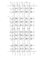
NAND型フラッシュメモリ装置(不揮発性記憶装置、半導体記憶装置、半導体装置)は、メモリセル領域および周辺回路領域に区画されている。図2は、メモリセル領域におけるメモリセルアレイの配置形態の一例を示している。メモリセルアレイArは、ビット線BL側やソース線S側にそれぞれ接続された選択ゲートトランジスタTrsおよびTrsと、これらの選択ゲートトランジスタTrsおよびTrs間に複数個直列接続されたメモリセルトランジスタTrnとから構成されている。これらのメモリセルアレイArが図2に示すように縦列方向に配列されることによりメモリセル領域が形成される。
(First embodiment)
A first embodiment in which the present invention is applied to a NAND flash memory device will be described below with reference to FIGS.
A NAND flash memory device (nonvolatile memory device, semiconductor memory device, semiconductor device) is partitioned into a memory cell region and a peripheral circuit region. FIG. 2 shows an example of an arrangement form of the memory cell array in the memory cell region. The memory cell array Ar is composed of selection gate transistors Trs and Trs connected to the bit line BL side and the source line S side, respectively, and a plurality of memory cell transistors Trn connected in series between the selection gate transistors Trs and Trs. Has been. These memory cell arrays Ar are arranged in the column direction as shown in FIG. 2 to form a memory cell region.
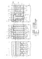
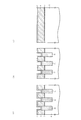
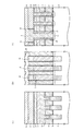
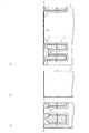
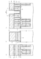
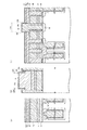
図1は、この回路例におけるメモリセルアレイの概略配置の一部(図2のX領域)を模式的な平面図により示している。この図3において、GCはコントロールゲート電極配線、FGはフローティングゲート電極、SGは選択ゲート配線、CBはビット線コンタクト形成領域、AAはアクティブエリア(活性領域)、STIは素子分離領域を示している。
また、図1(a)は、図3におけるA−A線に沿う模式的な縦断側面図を示しており、図1(b)は、図3におけるB−B線に沿う模式的な縦断側面図を示しており、さらに図1(c)は、図3におけるC−C線に沿う模式的な縦断側面図を示している。
FIG. 1 is a schematic plan view showing a part of the schematic arrangement of the memory cell array (X region in FIG. 2) in this circuit example. In FIG. 3, GC is a control gate electrode wiring, FG is a floating gate electrode, SG is a selection gate wiring, CB is a bit line contact formation region, AA is an active area (active region), and STI is an element isolation region. .
Moreover, Fig.1 (a) has shown the typical vertical side view which follows the AA line in FIG. 3, FIG.1 (b) has shown the typical vertical side surface in alignment with the BB line in FIG. Further, FIG. 1C shows a schematic longitudinal side view taken along the line CC in FIG.
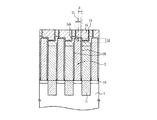
本実施形態においては、図1(a)〜図1(c)に示す上部導電層2(ビット線BLに相当)および接続配線層(後述する第3の多結晶シリコン層3に相当)の接続形態に特徴を備えているため、その接続形態の説明について詳細に行う。
図1(a)および図1(c)に示すように、各トランジスタTrs,Trnにおけるゲート電極形成領域Gには、p型のシリコン半導体基板4上にシリコン酸化膜5,第1の多結晶シリコン層6,ONO(Oxide Nitride Oxide)膜7,第2の多結晶シリコン層8,タングステンシリサイド(WSi)層9,第1のシリコンナイトライド膜10の順に下から積層形成されている。尚、選択ゲート形成領域Gにおいて、第1および第2の多結晶シリコン層6および8はその外部において電気的に接続されているが、この接続形態については図示していない。尚、p型のシリコン半導体基板4上に形成された実施形態を示すが、これはpウェル領域に形成されていても良いし、必要に応じて逆導電型のシリコン半導体基板に形成されていても良い。
In the present embodiment, the connection between the upper conductive layer 2 (corresponding to the bit line BL) and the connection wiring layer (corresponding to a third
As shown in FIGS. 1A and 1C, the gate electrode formation region G in each of the transistors Trs and Trn has a
シリコン酸化膜5は、例えば8nmの膜厚により形成されており、各トランジスタTrs,Trnのゲート絶縁膜として機能する。
第1の多結晶シリコン層6は、p型の不純物がドープされた多結晶シリコンにより例えば160nmの膜厚で形成されており、トランジスタTrnのフローティングゲート電極FGとして機能する。
The
The first
ONO膜7は、図1(a)に示すように、第1の多結晶シリコン層6の側壁にも形成されている。このONO膜7は、素子分離領域(STI)として機能する第2のシリコン酸化膜11と共に第1の多結晶シリコン層6を覆うように例えば17nm(Oxide5nm:SiN7nm:Oxide5nm)の膜厚により形成され、トランジスタTrnのゲート電極形成領域Gにおける第1および第2の多結晶シリコン層6および8(フローティングゲート電極FGおよびコントロールゲート電極GC)を電気的に絶縁するために形成されている。
The
第2の多結晶シリコン層8は、p型の不純物がドープされた多結晶シリコンにより例えば100nm膜厚で形成されており、トランジスタTrnのゲート電極形成領域Gにおいては、タングステンシリサイド層9と共にコントロールゲート電極GCとして機能し、トランジスタTrsのゲート電極形成領域においてはタングステンシリサイド層9と共に選択ゲート電極SGとして機能し、所謂ワード線として形成される。タングステンシリサイド層9は、例えば90nmの膜厚により形成されている。また、第1のシリコンナイトライド膜10は、絶縁膜として機能する。
The second
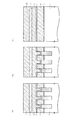
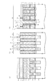
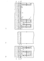
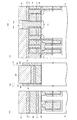
各トランジスタTrs,Trnのゲート電極形成領域Gに形成された各層6〜10を覆うように、第2のシリコンナイトライド膜12が形成されている。この第2のシリコンナイトライド膜12は、隣接するトランジスタTrs,Trn…のゲート電極形成領域G間を電気的に絶縁するようになっておりゲート電極分離用絶縁膜として機能する。
また、図1(b)および図1(c)並びに図3に示すように、隣接するトランジスタTrsおよびTrsのゲート電極形成領域G間(隣接する選択ゲートSG間)には、ビット線コンタクト形成領域CBが設けられている。
A second
Further, as shown in FIGS. 1B, 1C, and 3, a bit line contact formation region is provided between the gate electrode formation regions G of adjacent transistors Trs and Trs (between adjacent selection gates SG). CB is provided.
このビット線コンタクト形成領域CBには孔部13が形成されており、この孔部13に接続配線層として第3の多結晶シリコン層3が埋込み形成されている。この第3の多結晶シリコン層3は、図1(c)に示すように、トランジスタTrsおよびTrsを構成する各層6〜10を覆う第2のシリコンナイトライド膜12の間に埋込み形成される。第3の多結晶シリコン層3は縦長楕円柱状に縦長片部3b(本発明の下配線部に相当)として形成されると共に、この上部に円板状に上板部3a(本発明の上配線部に相当)として形成されることにより、第3の多結晶シリコン層3は縦断面T字形状に形成される。第3の多結晶シリコン層3はシリコン半導体基板4に形成された拡散層14(本発明の下部導電層に相当)と上部導電層2を構成するチタン層15とを電気的に接続している。
A
この第3の多結晶シリコン層3の上板部3aは、図1(c)に示すように、トランジスタTrsのゲート電極形成領域Gの第2のシリコンナイトライド膜12の上部にまで水平方向に形成されている。また、図1(b)に示すように、隣接するビット線コンタクト形成領域CB間には第2のシリコン酸化膜17、第3のシリコン酸化膜18(本発明の第1の絶縁膜に相当)および第4のシリコン酸化膜19が埋込み形成されている。これらの第2,第3および第4のシリコン酸化膜17〜19は、隣接する第3の多結晶シリコン層3を電気的に絶縁するために設けられている。
As shown in FIG. 1C, the
図1(b)および図1(c)に示すように、第3の多結晶シリコン層3の縦長片部3bの外周面には第3のシリコンナイトライド膜20が形成されている。この第3のシリコンナイトライド膜20は、図1(b)に示すように、第3の多結晶シリコン層3と、第2および第3のシリコン酸化膜17および18との間に縦長状に形成されると共に第3の多結晶シリコン層3の側壁に形成されるもので、隣接する第3の多結晶シリコン層3間の電気的絶縁機能を強化するためのスペーサとして機能する。
As shown in FIGS. 1B and 1C, a third
また、第3の多結晶シリコン層3の上板部3aにおける側壁外周面下部には第3のシリコンナイトライド膜20(本発明の第2の絶縁膜に相当)が形成されている。この第3のシリコンナイトライド膜20も前述したシリコンナイトライド膜と同様に、隣接する第3の多結晶シリコン層3間のスペーサとして機能するようになっている。
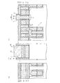
図1(c)に示すように、1つのメモリセルアレイを構成する各トランジスタTrnおよびTrsのゲート電極形成領域G間には、第2のシリコン酸化膜17が埋込み形成されている。この部位に埋め込まれる第2のシリコン酸化膜17は、各トランジスタTrsおよびTrn…のゲート電極形成領域G間の電気的絶縁機能を向上するために埋込み形成されており、第2のシリコンナイトライド膜12の上面に対して面一になるように埋込み形成されている。
A third silicon nitride film 20 (corresponding to the second insulating film of the present invention) is formed on the lower portion of the side wall outer peripheral surface of the
As shown in FIG. 1C, a second
第2のシリコンナイトライド膜12および第2のシリコン酸化膜17の上部には、ビット線コンタクト形成領域CB以外の領域に対して第3のシリコン酸化膜18が形成されている。この第3のシリコン酸化膜18は、第3の多結晶シリコン層3の側方に水平方向に薄板状に形成されており、各種ゲート電極(コントロールゲート電極GC,選択ゲート電極SG,フローティングゲート電極FG)やタングステンシリサイド層9とビット線BL(タングステン層16およびチタン層15)との間の絶縁性能を保持するために設けられている。
A third
また、図1(b)および図1(c)に示すように、第3の多結晶シリコン層3の上板部3aのうちの上面部3aaおよび上側面部3abに接触するように上部導電層としてタングステン(W)層16およびチタン(Ti)層15が形成されている。
これらのタングステン層16およびチタン層15は、所謂ビット線BLとして機能する。チタン層15は例えば45nmの膜厚により形成され、第3の多結晶シリコン層3の上板部3aのうちの上面部3aaおよび上側面部3ab,並びに第3のシリコンナイトライド膜20の上部に接触するように形成されていると共に、第3のシリコン酸化膜18の上部に例えば45nmの膜厚により形成されている。このチタン層15は、第3のシリコン酸化膜18とタングステン層16との間に両層16および18が非接触状態を保つように形成されている。タングステン層16は、例えば400nmの膜厚により形成され、その下部がチタン層15に覆われるように形成されている。
Further, as shown in FIGS. 1B and 1C, the upper conductive layer is in contact with the upper surface portion 3aa and the upper side surface portion 3ab of the
These
第1の実施形態の構成によれば、第3の多結晶シリコン層3の上板部3aの全側壁が第3のシリコンナイトライド膜20により覆われてはおらず、第3の多結晶シリコン層3の上板部3aの上面部3aaおよび上側面部3abにおいてチタン層15が第3の多結晶シリコン層3に接触するようになっているため、第3の多結晶シリコン層3およびチタン層15間の接触面積を増加させることができる(図1(b)および図1(c)の接触面積S2を参照)。
According to the configuration of the first embodiment, the entire side wall of the
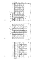
<詳細な製造方法について>
以下、図4ないし図19をも参照しながら、詳細な製造方法について説明する。尚、図4〜図16の図面中、同一の添え字(a)〜(c)を付した図面については、それぞれ図3の平面図におけるA−A線,B−B線,C−C線に沿う縦断側面図を示している。尚、前記した構成を形成することができれば、以下に示す工程については必要に応じて省いても良いし付加しても良い。
<Detailed manufacturing method>
Hereinafter, a detailed manufacturing method will be described with reference to FIGS. In addition, about drawing which attached | subjected the same subscript (a)-(c) in drawing of FIGS. 4-16, the AA line, the BB line, and CC line in the top view of FIG. 3, respectively. The longitudinal side view along line is shown. As long as the above-described configuration can be formed, the following steps may be omitted or added as necessary.
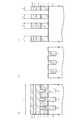
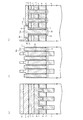
(1)図4に示す構造を形成する工程について
p型のシリコン半導体基板4の上にシリコン酸化膜5を例えば8nm形成する。そして、減圧CVD(Low Pressure Chemical Vapor Deposition)法によりp型の不純物がドープされた第1の多結晶シリコン層6を例えば160nm形成し、さらに第4のシリコンナイトライド膜21を例えば70nm形成する。そして、その上にフォトレジスト(図示せず)を塗布しリソグラフィ技術により所定のレジストパターンに加工し、このレジストパターンをマスクとしてRIE(Reactive Ion Etching)法により第4のシリコンナイトライド膜21,第1の多結晶シリコン層6,第1のシリコン酸化膜5,およびシリコン半導体基板4を同時に所定の深さまで加工することにより素子分離領域STIを形成するための溝部22を形成し、フォトレジストを除去する。すると図4に示すように形成される。
(1) Step of forming the structure shown in FIG. 4 A
(2)図5に示す構造を形成する工程について
(1)の形成工程終了後、HDP(High Density Plasma)−CVD法により第2のシリコン酸化膜11を溝部22に埋込むように例えば550nm堆積する。そして、第4のシリコンナイトライド膜21が露出するようにCMP(Chemical Mechanical Polishing)法により第2のシリコン酸化膜11を平坦化し、窒素雰囲気において例えば900℃に加熱する。次に、例えば150℃のリン酸処理により第4のシリコンナイトライド膜21を除去する。そして、フォトレジスト(図示せず)を塗布し、リソグラフィ技術により所定のレジストパターンに加工し、このレジストパターンをマスクとしてRIE法により第2のシリコン酸化膜11を落とし込む。フォトレジストを除去後、減圧CVD法により第2のゲート絶縁膜としてのONO膜7を17nm(Oxide:5nm,SiN:7nm,Oxide:5nm)等方的に形成する。すると図5に示すように形成される。
(2) Regarding the process of forming the structure shown in FIG. 5 After the formation process of (1), the second
(3)図6に示す構造を形成する工程について
(2)の形成工程終了後、酸化性雰囲気において加熱する。そして、ONO膜7の上に減圧CVD法によりP型の不純物がドープされた第2の多結晶シリコン層8を例えば100nm形成する。そして、第2の多結晶シリコン層8の上にスパッタ法によりタングステンシリサイド層9を例えば90nm形成する。そして、減圧CVD法により第1のシリコンナイトライド膜10を300nm形成する。すると、図6に示すように形成される。
(3) Regarding the process of forming the structure shown in FIG. 6 After the formation process of (2), heating is performed in an oxidizing atmosphere. Then, a second
(4)図7に示す構造を形成する工程について
(3)の形成工程終了後、フォトレジスト(図示せず)を塗布しリソグラフィ技術によりフォトレジストを所定のレジストパターンに加工し、このフォトレジストをマスクとしてRIE法により第1のシリコンナイトライド膜10をエッチングする。このエッチングは、ゲート電極形成領域G以外の領域について行われる。フォトレジストをアッシングにより除去した後、第1のシリコンナイトライド膜10をマスクとしてタングステンシリサイド層9,第2の多結晶シリコン層8,ONO膜7,および第1の多結晶シリコン層6をRIE法によりエッチングする(図7(b)および図7(c)参照)。
(4) Regarding the process of forming the structure shown in FIG. 7 After the completion of the formation process of (3), a photoresist (not shown) is applied, and the photoresist is processed into a predetermined resist pattern by a lithography technique. The first
このとき、ビット線BLを接続形成するためのビット線コンタクト形成領域CBおよびその周辺においては、第1のシリコンナイトライド膜10やタングステンシリサイド層9,第2の多結晶シリコン層8,ONO膜7,および第1の多結晶シリコン層6をRIE法によりエッチングし、図7(b)に示すように、シリコン酸化膜5を除きシリコン半導体基板4上に形成された全層を除去する。すると図7に示すように形成される。
At this time, the first
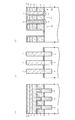
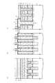
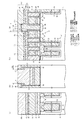
(5)図8に示す構造の形成工程について
(4)の形成工程終了後、例えば1050℃程度のRTO(Rapid Thermal Oxidation)処理を行う。そして、第2のシリコンナイトライド膜12を例えば20nm等方的に形成する。その後、隣接するトランジスタTrnおよびTrsのゲート電極形成領域G間に形成された第2のシリコン窒化膜12および第2のシリコン酸化膜17を介してシリコン半導体基板4にn型の不純物を打込むことによりトランジスタTrnおよびTrsのソース/ドレイン拡散層22を形成する。
(5) Regarding the formation process of the structure shown in FIG. 8 After the completion of the formation process of (4), for example, an RTO (Rapid Thermal Oxidation) process at about 1050 ° C. is performed. Then, the second
その後、トランジスタTrnおよびTrsのゲート電極形成領域G間に形成された第2のシリコンナイトライド膜12の上部に第2のシリコン酸化膜17を埋込み形成すると共に、トランジスタTrnおよびTrnのゲート電極形成領域G間に形成された第2のシリコンナイトライド膜12の上部に第2のシリコン酸化膜17を埋込み形成する。
このとき、図8(b)に示すように、第2のシリコン酸化膜17を形成する。この第2のシリコン酸化膜17は、隣接する第3の多結晶シリコン層3間の電気的絶縁用として設けられている。
Thereafter, a second
At this time, as shown in FIG. 8B, a second
そして、燃焼酸化雰囲気において800℃程度でリフロー処理し、第2および第1のシリコンナイトライド膜12および10をストッパとしてCMP法により第2のシリコン酸化膜17を平坦化する。その後、第2および第1のシリコンナイトライド膜12および10や第2のシリコン酸化膜17の上部に対してプラズマCVD法により第3のシリコン酸化膜18を形成する。フォトレジスト(図示せず)を塗布しリソグラフィ技術により所定のレジストパターンに加工し、第3のシリコン酸化膜18を除去する。すると図9に示すように形成される。
Then, a reflow process is performed at about 800 ° C. in a combustion oxidation atmosphere, and the second
(5)の形成工程終了後、図10に示すように、第3のシリコンナイトライド膜20を例えば10nm等方的に形成する。さらに、図11に示すように、第3のシリコンナイトライド膜20をドライエッチングすることにより、第3のシリコン酸化膜18上に形成された第3のシリコンナイトライド膜20と、トランジスタTrsのゲート電極形成領域G上に形成された第3のシリコンナイトライド膜20と、シリコン半導体基板4の直上部に形成された第1のシリコン酸化膜5とをゲート電極形成領域Gの側壁絶縁膜として形成される部分を除き除去する。すると、図11に示すように、第3のシリコン酸化膜18のビット線コンタクト形成領域CB側の側壁、および2のトランジスタTrsのゲート電極形成領域G間に挟まれたビット線コンタクト形成領域CB側の側壁に第2および第3のシリコンナイトライド膜12および20が残存する。
After completion of the forming step (5), as shown in FIG. 10, a third
さらに、図12に示すように、第3の多結晶シリコン層3をビット線コンタクト形成領域CBに埋込み形成し、CDE(Chemical Dry Etching)法により第3の多結晶シリコン層3の上部をエッチバックし高さを調整する。その後、窒素性雰囲気において970℃の熱処理を行いドーパントを活性化させる。
さらに、図13に示すように、プラズマCVD法により第3のシリコン酸化膜18,第3のシリコンナイトライド膜20,および第3の多結晶シリコン膜3の上に、さらに第4のシリコン酸化膜19を形成することによりシリコン酸化膜の厚さを増加させる。
Further, as shown in FIG. 12, the third
Further, as shown in FIG. 13, a fourth silicon oxide film is further formed on the third
その後、フォトレジスト(図示せず)を塗布し当該フォトレジストに所定のレジストパターンを形成しこのレジストパターンをマスクとしてRIE法により第3および第4のシリコン酸化膜18および19を、多結晶シリコンおよびシリコン窒化膜に対して高選択性を有するエッチング条件によりエッチバックしビット線BLの領域を形成する。
このときビット線コンタクト形成領域CB周辺では、第3の多結晶シリコン層3の上板部3aの上面部3aaよりも下方まで第3のシリコン酸化膜18をエッチバックする。第3のシリコン窒化膜20は、第3の多結晶シリコン層3の上板部3aの上方部分については第3および第4のシリコン酸化膜18および19と略同時に除去されるが、第3の多結晶シリコン層3の上板部3aの側壁に第3のシリコン窒化膜20が付着し残存するようになる。
Thereafter, a photoresist (not shown) is applied to form a predetermined resist pattern on the photoresist. Using this resist pattern as a mask, the third and fourth
At this time, around the bit line contact formation region CB, the third
その後、図15に示すように、シリコン酸化膜や多結晶シリコンに対して高選択性を有するエッチング条件により(例えば、150℃のリン酸処理等によるウェットエッチング処理)、第3のシリコン酸化膜18の上面より下方で、且つ、第2のシリコンナイトライド膜12の上面より上方まで第3のシリコンナイトライド膜20を除去する。尚、ドライエッチングにより第3のシリコンナイトライド膜20を除去するようにしても良い。すなわち、第3の多結晶シリコン層3の側壁の上部について第3のシリコンナイトライド膜20を除去する。すると図15に示すように形成される。
Thereafter, as shown in FIG. 15, the third
この後、図16に示すように、PVD法によりTi膜15を例えば45nm等方的に形成する。そして水素を含む窒素性雰囲気において550℃,90分加熱する。さらに、図1に示すように、PVD法によりW(タングステン)膜16を例えば400nm等方的に形成し、その後、タングステン膜16およびTi膜15を第4の多結晶シリコン酸化膜19が露出するまでCMP法により平坦化する。そして、水素を含む窒素性雰囲気中において400℃,30分熱処理する。さらに後工程を行うことにより、NAND型不揮発性記憶装置1のメモリセル領域を形成することができるようになる。
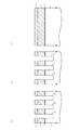
Thereafter, as shown in FIG. 16, a
従来、第3の多結晶シリコン層3の上板部3aの外周面の側壁に第3のシリコンナイトライド膜20をスペーサとして形成してしまうと、第3の多結晶シリコン層3は上板部3aの上面部3aaとのみしかチタン層15と接触しないため接触部分の高抵抗化を免れない。
そこで本実施形態の製造方法では、第2のシリコンナイトライド膜12および第2のシリコン酸化膜17の上部にビット線コンタクト形成領域CBを除いて第3のシリコン酸化膜18を形成し、ビット線コンタクト形成領域CBにスペーサとして第2のシリコンナイトライド膜12を等方的に形成し、シリコン半導体基板4の上面に位置する第2および第3のシリコンナイトライド膜12および20を除去し、ビット線コンタクト形成領域CBにソース/ドレイン拡散層14と接触すると共に第2のシリコンナイトライド膜12の上方まで上板部3aの上面部3aaが形成されるように第3の多結晶シリコン層3を埋込み形成し、第3のシリコン酸化膜18を第3の多結晶シリコン層3の上面部3aaから水平方向下方に上面が位置するように第3のシリコン酸化膜18を除去し、第3の多結晶シリコン層3の上面部3aaから水平方向下方まで第3のシリコンナイトライド層20を除去し、第3の多結晶シリコン層3の上側面部3abにチタン層15を形成するため、第3の多結晶シリコン層3およびチタン層15間の接触面積を増加させることができ、これにより接触部分の抵抗を低減することができるようになる。
Conventionally, if the third
Therefore, in the manufacturing method of the present embodiment, the third
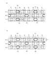
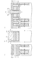
また、ビット線BL(チタン層15およびタングステン層16)を形成するときに、図17(a)に模式的な平面図を示すように、ビット線コンタクト形成領域CBに対してビット線BLの形成領域のリソグラフィ技術によるマスク合わせずれが生じない場合には問題ないものの、図17(b)に示すように、特に隣接するビット線コンタクト形成領域CB側にリソグラフィ技術によるマスクの合わせずれが特にワード線方向(ゲート電極形成方向)に生じると、第3の多結晶シリコン層3およびチタン層15の接触形態の基本構成例の模式的な断面図を図19に示すように、第3の多結晶シリコン層3およびチタン層15の接触部分が上面部3aaのみに留まってしまうと、第3の多結晶シリコン層3の上面部3aaでは接触するが接触面積S1が少なくなってしまう。
When the bit line BL (
本実施形態の製造方法によれば、マスクずれが生じると接触面積の低下に伴う抵抗値の増大が懸念されるものの第3の多結晶シリコン層3の外周面側壁の上側面部3abについて第3のシリコンナイトライド膜20の上部を除去し、その上側面部3abにおいても第3の多結晶シリコン層3およびチタン層15が接触するため、第3の多結晶シリコン層3の上面部3aaおよびチタン層15間の接触面積(接触面積S1参照)が少なくなったとしても上側面部3abでも接触する(接触面積S2参照)ようになるため、接触面積の低下を抑制できるようになる。
According to the manufacturing method of the present embodiment, although there is a concern about an increase in resistance value due to a decrease in contact area when mask displacement occurs, the third side surface 3ab of the upper side surface 3ab of the outer peripheral surface side wall of the third
(第2の実施形態)
図20は、本発明の第2の実施形態の説明図を示すもので、上記実施形態と異なるところは製造工程にある。以下、上記実施形態と同一部分については同一符号を付して説明を省略し、以下異なる部分について説明する。
本実施形態においては、図12を使用して説明を行った製造工程終了後、前述実施形態に説明した工程に代えて次に示す製造工程を行う。
(Second Embodiment)
FIG. 20 shows an explanatory diagram of the second embodiment of the present invention. The difference from the above embodiment is the manufacturing process. Hereinafter, the same parts as those in the above embodiment are denoted by the same reference numerals, description thereof will be omitted, and different parts will be described below.
In the present embodiment, after the manufacturing process described with reference to FIG. 12, the following manufacturing process is performed instead of the process described in the previous embodiment.
すなわち、図20に示すように、第3の多結晶シリコン層3および第3のシリコン酸化膜18に対して高選択性を有するエッチング条件により第3の多結晶シリコン層3の上面部3aaから下方にかけて第3のシリコンナイトライド膜20の上部(第3の多結晶シリコン層3の上側面部3ab)を除去する。そして、図示はしないが、前述実施形態と同様にビット線BL領域を除いて第3のシリコン酸化膜18の上部に第4のシリコン酸化膜19を形成した後、第3および第4のシリコン酸化膜18および19を第3の多結晶シリコン層3および第3のシリコンナイトライド膜20に対して高選択性を有するエッチング条件下において除去する。そして前述実施形態と同様にチタン層15およびタングステン層16を埋込み形成する。このような第2の実施形態においても、前述実施形態と略同様な作用効果を奏する。
That is, as shown in FIG. 20, the upper surface portion 3aa of the third
(第3の実施形態)
図21〜図31は、本発明の第3の実施形態の説明図を示すもので、上記各実施形態と異なるところは、トレンチ型のDRAM半導体記憶装置に適用したところにある。
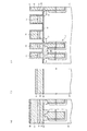
まず、図21および図22を参照しながらDRAM半導体記憶装置31の機能的な構造について説明する。図22は、DRAM半導体記憶装置の模式的な平面図を示しており、図21(a)は、この図22におけるD−D線に沿う断面図を示しており、図21(b)は、図22におけるE−E線に沿う断面図を示しており、図21(c)は、図22におけるF−F線に沿う断面図を示している。
(Third embodiment)
FIGS. 21 to 31 are explanatory views of the third embodiment of the present invention. The difference from each of the above embodiments is that it is applied to a trench type DRAM semiconductor memory device.
First, the functional structure of the DRAM
この図21において、半導体装置としてのDRAM半導体記憶装置30は、メモリセル領域においては、1メモリセルとして1のMOS型のセルトランジスタTrおよび1のトレンチキャパシタCが形成されており、これらのメモリセルが複数配列されている。シリコン半導体基板31には、深いトレンチ32(溝部)が形成されており、このトレンチ32の底部側に位置してトレンチキャパシタCが形成されている。尚、トレンチ4は、図22に示すように楕円形状に形成されている。
In FIG. 21, a DRAM semiconductor memory device 30 as a semiconductor device has one MOS cell transistor Tr and one trench capacitor C formed as one memory cell in the memory cell region. Are arranged. A deep trench 32 (groove) is formed in the
以下、トレンチキャパシタCの構成について概略的に説明する。トレンチ32の外周には、当該トレンチ32の底部側からある所定の高さまでプレート拡散層33が形成されている。このプレート拡散層33はトレンチキャパシタCのプレート電極として機能する。トレンチ32の内面で且つプレート拡散層33の上には、キャパシタ絶縁膜34が形成されている。このキャパシタ絶縁膜34は、SiN−SiO2膜またはAl2O3−SiO2膜、またはHfO2−SiO2膜等により形成されており、トレンチキャパシタCの両プレート電極分離用の絶縁膜として機能する。
Hereinafter, the configuration of the trench capacitor C will be schematically described. A
トレンチ32の内面且つキャパシタ絶縁膜34の上には、多結晶シリコン層またはポリサイド材料による第1の導電層35が埋込み形成されている。この第1の導電層35は、トレンチキャパシタCのプレート電極として機能する。このようにしてトレンチキャパシタCは、第1の導電層35、キャパシタ絶縁膜34、プレート拡散層33により構成されている。
A first
第1の導電層35の上部には、素子分離領域36(STI(Shallow Trench Isolation))が形成されている。図21に示すように、この素子分離領域36は、セルトランジスタTrが形成される側とは逆側に形成される層であり、トレンチキャパシタCと隣接した他のメモリセルとの間で電気的に絶縁分離するように形成されている。また、この素子分離領域36は、図21(c)に示すように、この素子分離領域36上を通過するように形成されたワード線WL(ゲート電極G2)とトレンチキャパシタCとを電気的に絶縁分離する機能を有しているものである。
Over the first
セルトランジスタTrは、トレンチキャパシタCに対して隣接して配設されていると共に電気的に接続するようにトレンチ32の所定方向側に形成されている。セルトランジスタTrは、ワード線WLとしても機能するゲート電極G2、n型の拡散層37および38(ソース/ドレイン拡散層)、並びにゲート絶縁膜として機能する第1のシリコン酸化膜39を備えている。一方の拡散層37には、トレンチキャパシタCを構成する第1の導電層38が接続されている。
The cell transistor Tr is disposed adjacent to the trench capacitor C and is formed on a predetermined direction side of the
また、他方の拡散層38(本発明の下部導電層に相当)の上部にはビット線BL2に電気的に接続するための第2の多結晶シリコン層40(ビット線コンタクト:本発明の接続配線層に相当)が埋込み形成されている。他方の拡散層38には、当該第2の多結晶シリコン層40を介して上層側のビット線BL2を構成するチタン層41が接触しており、この第2の多結晶シリコン層40を介して拡散層38とチタン層41とが電気的に接続されている。
On the other side of the other diffusion layer 38 (corresponding to the lower conductive layer of the present invention), a second polycrystalline silicon layer 40 (bit line contact: connection wiring of the present invention) for electrical connection to the bit line BL2 is provided. (Corresponding to the layer) is embedded. The
また、ゲート電極G2を覆うようにゲート電極分離用絶縁膜としてゲート側壁絶縁膜42が形成されている。このゲート側壁絶縁膜42は、第1のシリコンナイトライド膜として形成されており、隣接するゲート電極G2間を絶縁分離するために設けられている膜である。
さらに、ビット線BL2とメモリセルを電気的に絶縁分離するように層間絶縁膜43(本発明の第1の絶縁膜に相当)が形成されている。第2の導電層40の側壁外周面にはスペーサとして第2のシリコンナイトライド膜44(本発明の第2の絶縁膜に相当)が形成されている。この第2のシリコンナイトライド膜44は、チタン層41と第2の導電層40の上面部40aおよび上側面部40bにおいて接触するようになっている。
A gate
Further, an interlayer insulating film 43 (corresponding to the first insulating film of the present invention) is formed so as to electrically insulate and isolate the bit line BL2 and the memory cell. A second silicon nitride film 44 (corresponding to the second insulating film of the present invention) is formed as a spacer on the outer peripheral surface of the side wall of the second
また、チタン層41の上部にはタングステン層45が形成されている。これらチタン層41およびタングステン層45によりビット線BL2が構成されている。このようにして1のメモリセルが構成されており、図22に示すように複数のメモリセルが密接するように配設されている。尚、図22において、アクティブエリアAAは、メモリセルの活性領域を示している。
A
このような場合、図22(a)に示すように、ビット線BL2(チタン層41およびタングステン層45)が図中上下方向にマスク合わせずれが生じることなく形成される場合には、ビット線BL2と隣接する第2の導電層40間の距離も長いため、その電気的相互作用も無視できるが、近年の設計ルールの縮小化に伴いその距離が短くなってきているため、図22(b)に示すようにビット線BL2の形成時にマスクの合わせずれδ2が生じると、ビット線BL2と隣接する第2の導電層40間の距離も短くなってしまうと共に、ビット線BL2と第2の導電層40との接触面積も低下してしまう。本実施形態では、上面部40aだけでなく上側面部40bでもビット線BL2と第2の導電層40とが接触するようになっているため、ビット線BL2と第2の導電層40との接触面積の低下を抑制することができ、接触部分の抵抗を極力抑えることができるようになる。
In such a case, as shown in FIG. 22A, when the bit line BL2 (
<製造方法(プロセス)について>
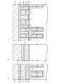
以下、前述した機能的部分を形成する場合の実質的な層の形成方法について図21ないし図31を参照しながら説明する。本実施形態では、特にビット線BL2(後述するチタン層41)とコンタクトプラグ(後述する第2の多結晶シリコン層40)とを接続する構成部分およびその周辺関連部分に特徴があるため、トレンチキャパシタCやゲート電極G2の形成方法については省略し、本実施形態の特徴部分に関連するシリコン半導体基板31の上層部分について、その説明を行う。
<Manufacturing method (process)>
Hereinafter, a substantial layer forming method for forming the above-described functional portion will be described with reference to FIGS. In the present embodiment, there is a particular feature in the component connecting the bit line BL2 (
(1)図23ないし図25に示す構造の形成方法について
図23に示すように、p型のシリコン半導体基板31上に例えば8nm膜厚のシリコン酸化膜をゲート絶縁膜39として形成すると共に、トレンチキャパシタCや素子分離領域36を形成した後ゲート電極G2を形成する。
このゲート電極G2は次のように形成される。
(1) Method for Forming the Structure Shown in FIGS. 23 to 25 As shown in FIG. 23, a silicon oxide film having a thickness of, for example, 8 nm is formed as a
The gate electrode G2 is formed as follows.
図24に示すように、減圧CVD法によりp型の不純物がドープされた第1の多結晶シリコン層46をゲート絶縁膜39の上部に100nm形成し、第1の多結晶シリコン層46の上部に対してタングステンシリサイド層47を55nm形成する。タングステンシリサイド層47の上部に第3のシリコンナイトライド膜48を減圧CVD法により200nm形成する。そして、フォトレジスト(図示せず)を塗布し、リソグラフィ技術により所定のレジストパターンに加工し、このレジストパターンをマスクとして第3のシリコンナイトライド膜48をRIE法によりエッチングする。
As shown in FIG. 24, a first
すると、第1の多結晶シリコン層46およびタングステンシリサイド層48が分断され、これらの第1の多結晶シリコン層46およびタングステンシリサイド層48によりゲート電極G2が構成されると共に、各ゲート電極G2間の第3のシリコンナイトライド膜48が除去される。
その後、フォトレジストをアッシングにより剥離し、残存した第3のシリコンナイトライド膜48をマスクとしてタングステンシリサイド層47,p型の不純物がドープされた第1の多結晶シリコン層46をRIE法により加工する。すると、各ゲート電極G2間の第1の多結晶シリコン層46およびタングステンシリサイド層47が除去される。その後、1050℃程度のRTO(Rapid Thermal Oxidation)処理を施した後、第1のシリコンナイトライド膜42を40nm程度等方的に形成する。すると図25に示すように、各ゲート電極G2間に第1のシリコンナイトライド膜42がゲート側壁絶縁膜として薄く形成されるようになる。
Then, the first
Thereafter, the photoresist is removed by ashing, and the
(2)図26に示す構造の形成方法について
(1)の形成工程後、各ゲート電極G2間に第4のシリコン酸化膜49を埋込み形成する。第1のシリコンナイトライド膜42の上部に形成された第4のシリコン酸化膜49を第1および第3のシリコンナイトライド膜42および48をストッパとしてCMP(Chemical Mechanical Polish)法により平坦化する。
(2) Method for Forming Structure Shown in FIG. 26 After the forming step (1), a fourth
その後、露出した第1もしくは第3のシリコンナイトライド膜42,48の上部および第4のシリコン酸化膜49の上部に、第2のシリコン酸化膜43aを例えば150nm形成する。その後、第2のシリコン酸化膜43aの上部に第3のシリコン酸化膜43bを350nm形成する。すると、図26に示すように形成される。尚、これらの第2および第3シリコン酸化膜43aおよび43bが形成工程が終了すると層間絶縁膜43として機能するようになる。
Thereafter, a second
(2)の形成工程後、第3のシリコン酸化膜43bの上部にフォトレジスト(図示せず)を塗布し、リソグラフィ技術によりフォトレジストを所定のレジストパターンに加工する。その後、フォトレジストをマスクとしてRIE法により第3および第2のシリコン酸化膜43bおよび43aを加工(除去)し、さらに、図27に示すように、ビット線コンタクト形成領域CB2として形成される部分に対してセルフアラインコンタクト形成技術により第4のシリコン酸化膜49を除去すると共に、この部分に第2のシリコンナイトライド膜44を等方的に形成する。この第2のシリコンナイトライド膜44がスペーサとして機能するようになる。
After the forming step (2), a photoresist (not shown) is applied on the third
そして、ゲート電極G2間の底部に形成された第2および第1のシリコンナイトライド膜44および42をドライエッチングする。すると、各ゲート電極G2の側壁に第2のシリコンナイトライド膜44がスペーサとして残存するようになり孔部が形成される。そして、この孔部を通じてn型の不純物をシリコン半導体基板31に拡散させることによりソース/ドレイン拡散層38を形成する。
Then, the second and first
その後、第2のシリコンナイトライド膜44の内側にp型の不純物がドープされた多結晶シリコンを埋込み形成することによりコンタクトプラグとして機能する第2の多結晶シリコン層40を埋込み形成する。そして、図28に示すように、CDE(Chemical Dry Etching)法により第2の多結晶シリコン層40の上部を除去することにより高さを調整する。さらに、970℃の窒素性雰囲気内で加熱処理を行いドーパントを活性化させる。
Thereafter, a second
そして、図29に示すように、多結晶シリコンおよびシリコン窒化膜に対して選択性の高いエッチング条件において、第2の多結晶シリコン層40の上面部40aよりも下方まで第2のシリコン酸化膜43bをエッチングにより除去する。すると、図29に示すように、第2のシリコンナイトライド膜44も同時に第2の多結晶シリコン層40の上面部40aまで除去されるようになる。
Then, as shown in FIG. 29, the second
そして、図30に示すように、第2の多結晶シリコン層40の外周面の上部側壁に形成された第2のシリコンナイトライド膜44を150℃のリン酸処理等のウェットエッチングにより除去する。このとき、第2の多結晶シリコン層40の上面部40aよりも下方まで第2のシリコンナイトライド膜44をシリコン酸化膜および多結晶シリコンに対して選択性の高いエッチング条件下におけるウェットエッチングにより除去し、第2の多結晶シリコン層40の側壁外周面の上側面部40bを露出させる。
Then, as shown in FIG. 30, the second
このとき、図30に示すように、第2のシリコンナイトライド膜44の上部が第3のシリコン酸化膜43bの上面より下方に位置するように第2のシリコンナイトライド膜44を除去することが望ましい。尚、このとき、第2のシリコンナイトライド膜44を除去するときにはドライエッチングにより除去しても良い。
さらに、図31に示すように、第2および第3のシリコン酸化膜43aおよび43bの上部並びに第2のシリコンナイトライド膜44の上部にチタン膜41をPVD法により例えば45nm程度等方的に堆積する。すると、第2の多結晶シリコン層40の上面部40aおよび上側面部40bに接触するようにチタン膜41が形成されるようになる。さらに、550℃,90分の水素を含む窒素性雰囲気内で加熱する。
At this time, as shown in FIG. 30, the second
Further, as shown in FIG. 31, a
続いて、図21に示すように、このチタン層41の上部にPVD法によりタングステン層45を例えば400nm程度堆積し、図21(b)に示すように、タングステン膜45およびチタン膜41を平坦化し、水素を含む窒素性雰囲気において400℃で30分間加熱する。このようにしてビット線コンタクト(コンタクトプラグ)としての第2の多結晶シリコン層40とビット線BL2との接触部分が構成される。
Subsequently, as shown in FIG. 21, a
このような第3の実施形態においても、ビット線コンタクトとしての第2の多結晶シリコン層40とビット線BL2とが第2の多結晶シリコン層40の上面部40aのみに留まらず第2の多結晶シリコン層40の上側面部40bにおいても接触するため、第1の実施形態と略同様の作用効果を奏すると共に、DRAM半導体記憶装置30にも適用できるようになる。
Also in the third embodiment, the second
(第4の実施形態)
図32は、本発明の第4の実施形態の説明図を示すもので、第3の実施形態と異なるところはその製造方法にある。上記実施形態と同一部分には同一符号を付して説明を省略し、以下異なる製造方法について説明する。
図28に示す構造を形成した後、シリコン半導体基板31の拡散層38の上面に位置する第2および第1のシリコンナイトライド膜44および42およびシリコン酸化膜39を除去し、第2の多結晶シリコン層40を埋込み形成する。そして、この第2の多結晶シリコン層40の上部を高さ調整した後、第2の多結晶シリコン層40の側壁外周面の上側面部40bに形成された第2のシリコンナイトライド膜44を除去する。この場合、シリコン酸化膜および多結晶シリコンに対して選択性の高いエッチング条件下においてエッチングすることにより第2のシリコンナイトライド膜44を除去し、第2の多結晶シリコン層40の上面部40aより下方に第2のシリコンナイトライド膜44の上部が位置するように第2のシリコンナイトライド膜44を除去し、第2の多結晶シリコン層40の上側面部40bを露出させる。
(Fourth embodiment)
FIG. 32 shows an explanatory diagram of the fourth embodiment of the present invention. The difference from the third embodiment resides in the manufacturing method. The same parts as those in the above embodiment are denoted by the same reference numerals, description thereof is omitted, and different manufacturing methods will be described below.
After the structure shown in FIG. 28 is formed, the second and first
その後、図21に示すように、多結晶シリコンおよびシリコンナイトライドに対して選択性の高いエッチング条件下において第3のシリコン酸化膜43bをエッチングすることにより、第3のシリコン酸化膜43bの上部を第2の多結晶シリコン層40の上面部40aの下方で、且つ、第2のシリコンナイトライド膜44の上方まで除去する。
そして、前述実施形態と同様に第3のシリコン酸化膜43bの上部および第2の多結晶シリコン層40の上面部40aおよび上側面部40bにチタン層41を形成し、その上部にタングステン層45を形成することにより前述実施形態と同様の構成を形成することができるようになる。このような第4の実施形態においても、第3の実施形態と略同様の作用効果を奏する。
Thereafter, as shown in FIG. 21, the third
Then, similarly to the above-described embodiment, the
図面中、2およびBLはビット線(上部導電層)、3は接続配線層、3aaは上面部、3abは上側面部、6は第1の多結晶シリコン層、8は第2の多結晶シリコン層、10は第1のシリコンナイトライド膜、11は第2のシリコン酸化膜(素子分離領域,STI)、12は第2のシリコンナイトライド膜(第2の絶縁膜,ゲート電極分離用絶縁膜)、13は孔部、14は拡散層(下部導電層)、18はシリコン酸化膜(第1の絶縁膜)、20はシリコンナイトライド膜(第2の絶縁膜)、Arはメモリセルアレイ、BLはビット線、CBおよびCB2はビット線コンタクト形成領域、Gはゲート電極形成領域、FGはフローティングゲート電極(ゲート電極)、GCはコントロールゲート電極(ゲート電極)、Sはソース線、SGは選択ゲート電極(ゲート電極)、Trsは選択ゲートトランジスタ、Trnはメモリセルトランジスタを示す。
In the drawing, 2 and BL are bit lines (upper conductive layers), 3 is a connection wiring layer, 3aa is an upper surface portion, 3ab is an upper side surface portion, 6 is a first polycrystalline silicon layer, and 8 is second polycrystalline silicon.
Claims (5)
前記上部導電層と上面部において接触すると共に前記下部導電層と接触するように形成され、前記上部導電層および下部導電層間を電気的に接続する接続配線層と、
前記接続配線層の側壁外周面に対して前記第1の絶縁膜とは異なる材質により隣接する接続配線層との間のスペーサとして形成された第2の絶縁膜とを備え、
前記接続配線層は、当該接続配線層の上面部および上側面部において前記上部導電層と接触するように構成されていることを特徴とする半導体装置。 A first insulating film formed between the upper conductive layer and the lower conductive layer;
A connection wiring layer formed so as to be in contact with the upper conductive layer and the lower conductive layer and electrically connecting the upper conductive layer and the lower conductive layer;
A second insulating film formed as a spacer between the connection wiring layer adjacent to the outer peripheral surface of the side wall of the connection wiring layer with a material different from the first insulating film;
The connection wiring layer is configured to be in contact with the upper conductive layer at an upper surface portion and an upper side surface portion of the connection wiring layer.
この半導体基板上に形成された複数のゲート電極と、
このゲート電極上に形成された第1の絶縁膜と、
この第1の絶縁膜上に形成されたビット線と、
前記半導体基板の表面の隣接するゲート電極間に形成された拡散層と、
前記ビット線と前記拡散層とを電気的に接続する接続配線層であって、隣接するゲート電極に挟まれた下配線部とこの下配線部の上に位置し側端が前記ゲート電極の上面上に張り出した上配線部とを有し、この上配線部の上面および側面の上部が前記ビット線に接続した接続配線層と、
前記下配線部と前記ゲート電極との間および前記側面の下部と前記ビット線との間に設けられた第2の絶縁膜とを具備したことを特徴とする半導体装置。 A semiconductor substrate;
A plurality of gate electrodes formed on the semiconductor substrate;
A first insulating film formed on the gate electrode;
A bit line formed on the first insulating film;
A diffusion layer formed between adjacent gate electrodes on the surface of the semiconductor substrate;
A connection wiring layer for electrically connecting the bit line and the diffusion layer, a lower wiring portion sandwiched between adjacent gate electrodes, and a side end located on the lower wiring portion is an upper surface of the gate electrode An upper wiring portion protruding above, and a connection wiring layer in which an upper surface and an upper portion of a side surface of the upper wiring portion are connected to the bit line;
A semiconductor device comprising: a second insulating film provided between the lower wiring portion and the gate electrode and between a lower portion of the side surface and the bit line.
前記下部導電層の上部に対して接続配線層を少なくとも第1の絶縁膜の上方まで埋込み形成する工程と、
隣接する接続配線層との間のスペーサとして前記接続配線層の側壁外周面に第2の絶縁膜を形成する工程と、
前記接続配線層の側壁外周面について当該接続配線層上面部から下方にかけて形成された前記第2の絶縁膜の上部を除去する工程と、
この第2の絶縁膜が除去された位置において前記接続配線層の上側面部に接触するように上部導電層を形成する工程とを備えたことを特徴とする半導体装置の製造方法。 Forming a first insulating film on the upper layer side of the lower conductive layer;
Burying and forming a connection wiring layer at least above the first insulating film above the lower conductive layer; and
Forming a second insulating film on the outer peripheral surface of the side wall of the connection wiring layer as a spacer between adjacent connection wiring layers;
Removing the upper part of the second insulating film formed from the upper surface of the connection wiring layer to the lower side with respect to the outer peripheral surface of the side wall of the connection wiring layer;
And a step of forming an upper conductive layer so as to be in contact with the upper side surface portion of the connection wiring layer at a position where the second insulating film is removed.
前記ゲート絶縁膜上のゲート電極形成領域にゲート電極を形成する工程と、
このゲート電極を覆うようにゲート電極分離用絶縁膜を形成する工程と、
前記ゲート電極分離用絶縁膜の上部にビット線コンタクト形成領域を除いて第1の絶縁膜を形成する工程と、
複数の前記ゲート電極分離用絶縁膜間に位置するビット線コンタクト形成領域に対して隣接するビット線コンタクト形成領域との間のスペーサとして第2の絶縁膜を形成する工程と、
前記ビット線コンタクト形成領域において下部導電層と接触すると共に前記ゲート電極分離用絶縁膜の上方まで上面部が形成されるように接続配線層を前記第2の絶縁膜内に埋込み形成する工程と、
前記接続配線層の上面部から下方に上面が位置するように第1の絶縁膜を除去する工程と、
前記接続配線層の上面部から下方まで当該接続配線層の上側面部に形成された前記第2の絶縁膜を除去する工程と、
前記第1および第2の絶縁膜の除去された前記接続配線層の上側面部に接触するように上部導電層を形成する工程とを備えたことを特徴とする半導体装置の製造方法。 Forming a gate insulating film on the semiconductor substrate;
Forming a gate electrode in a gate electrode formation region on the gate insulating film;
Forming a gate electrode isolation insulating film so as to cover the gate electrode;
Forming a first insulating film on the gate electrode isolation insulating film except for a bit line contact formation region;
Forming a second insulating film as a spacer between a bit line contact formation region adjacent to a bit line contact formation region located between the plurality of gate electrode isolation insulating films;
Embedding and forming a connection wiring layer in the second insulating film so as to be in contact with the lower conductive layer in the bit line contact formation region and to form an upper surface portion above the insulating film for gate electrode isolation;
Removing the first insulating film so that the upper surface is located below the upper surface of the connection wiring layer;
Removing the second insulating film formed on the upper side surface portion of the connection wiring layer from the upper surface portion to the lower side of the connection wiring layer;
And a step of forming an upper conductive layer so as to be in contact with the upper side surface of the connection wiring layer from which the first and second insulating films have been removed.
前記ゲート絶縁膜上のゲート電極形成領域に前記ゲート電極を形成する工程と、
このゲート電極を覆うようにゲート電極分離用絶縁膜を形成する工程と、
前記ゲート電極分離用絶縁膜の上部にビット線コンタクト形成領域を除いて第1の絶縁膜を形成する工程と、
複数の前記ゲート電極分離用絶縁膜間に位置するビット線コンタクト形成領域に対して隣接するビット線コンタクト形成領域との間のスペーサとして第2の絶縁膜を形成する工程と、
前記ビット線コンタクト形成領域において下部導電層と接触すると共に前記ゲート電極分離用絶縁膜の上方まで上面部が形成されるように接続配線層を前記第2の絶縁膜内に埋込み形成する工程と、
前記接続配線層の上面部から下方まで当該接続配線層の上側面部について前記第2の絶縁膜を除去する工程と、
前記接続配線層の上面部から下方に上面部が位置するように第1の絶縁膜を除去する工程と、
前記第1および第2の絶縁膜の除去された前記接続配線層の上側面部に接触するように上部導電層を形成する工程とを備えたことを特徴とする半導体装置の製造方法。
Forming a gate insulating film on the semiconductor substrate;
Forming the gate electrode in a gate electrode formation region on the gate insulating film;
Forming a gate electrode isolation insulating film so as to cover the gate electrode;
Forming a first insulating film on the gate electrode isolation insulating film except for a bit line contact formation region;
Forming a second insulating film as a spacer between a bit line contact formation region adjacent to a bit line contact formation region located between the plurality of gate electrode isolation insulating films;
Embedding and forming a connection wiring layer in the second insulating film so as to be in contact with the lower conductive layer in the bit line contact formation region and to form an upper surface portion above the insulating film for gate electrode isolation;
Removing the second insulating film on the upper side surface of the connection wiring layer from the upper surface to the lower side of the connection wiring layer; and
Removing the first insulating film so that the upper surface portion is located below the upper surface portion of the connection wiring layer;
And a step of forming an upper conductive layer so as to be in contact with the upper side surface of the connection wiring layer from which the first and second insulating films have been removed.
Priority Applications (2)
| Application Number | Priority Date | Filing Date | Title |
|---|---|---|---|
| JP2004107154A JP2005294518A (en) | 2004-03-31 | 2004-03-31 | Semiconductor device and method for manufacturing the same |
| US11/094,466 US7511330B2 (en) | 2004-03-31 | 2005-03-31 | Semiconductor device and method of fabricating the same |
Applications Claiming Priority (1)
| Application Number | Priority Date | Filing Date | Title |
|---|---|---|---|
| JP2004107154A JP2005294518A (en) | 2004-03-31 | 2004-03-31 | Semiconductor device and method for manufacturing the same |
Publications (1)
| Publication Number | Publication Date |
|---|---|
| JP2005294518A true JP2005294518A (en) | 2005-10-20 |
Family
ID=35135564
Family Applications (1)
| Application Number | Title | Priority Date | Filing Date |
|---|---|---|---|
| JP2004107154A Pending JP2005294518A (en) | 2004-03-31 | 2004-03-31 | Semiconductor device and method for manufacturing the same |
Country Status (2)
| Country | Link |
|---|---|
| US (1) | US7511330B2 (en) |
| JP (1) | JP2005294518A (en) |
Families Citing this family (4)
| Publication number | Priority date | Publication date | Assignee | Title |
|---|---|---|---|---|
| JP5016832B2 (en) | 2006-03-27 | 2012-09-05 | 株式会社東芝 | Nonvolatile semiconductor memory device and manufacturing method thereof |
| US7790516B2 (en) * | 2006-07-10 | 2010-09-07 | Qimonda Ag | Method of manufacturing at least one semiconductor component and memory cells |
| US7585746B2 (en) * | 2006-07-12 | 2009-09-08 | Chartered Semiconductor Manufacturing, Ltd. | Process integration scheme of SONOS technology |
| JP4504403B2 (en) * | 2007-08-29 | 2010-07-14 | 株式会社東芝 | Semiconductor memory device |
Citations (4)
| Publication number | Priority date | Publication date | Assignee | Title |
|---|---|---|---|---|
| JP2001093855A (en) * | 1999-09-20 | 2001-04-06 | Nec Corp | Method of manufacturing semiconductor device |
| JP2001274365A (en) * | 2000-03-28 | 2001-10-05 | Toshiba Corp | Non-volatile semiconductor memory device and producing method therefor |
| JP2002343861A (en) * | 2001-05-21 | 2002-11-29 | Mitsubishi Electric Corp | Semiconductor integrated circuit and its manufacturing method |
| JP2003197779A (en) * | 2001-12-25 | 2003-07-11 | Toshiba Corp | Semiconductor device and its manufacturing method |
Family Cites Families (9)
| Publication number | Priority date | Publication date | Assignee | Title |
|---|---|---|---|---|
| US5783471A (en) * | 1992-10-30 | 1998-07-21 | Catalyst Semiconductor, Inc. | Structure and method for improved memory arrays and improved electrical contacts in semiconductor devices |
| US5563089A (en) * | 1994-07-20 | 1996-10-08 | Micron Technology, Inc. | Method of forming a bit line over capacitor array of memory cells and an array of bit line over capacitor array of memory cells |
| US5338700A (en) * | 1993-04-14 | 1994-08-16 | Micron Semiconductor, Inc. | Method of forming a bit line over capacitor array of memory cells |
| JPH06310612A (en) | 1993-04-27 | 1994-11-04 | Hitachi Ltd | Wiring structure of semiconductor indegrated circuit and its manufacture |
| JPH1117140A (en) * | 1997-06-25 | 1999-01-22 | Sony Corp | Semiconductor device and manufacturing method thereof |
| US6028004A (en) * | 1998-01-06 | 2000-02-22 | International Business Machines Corporation | Process for controlling the height of a stud intersecting an interconnect |
| JP4931267B2 (en) * | 1998-01-29 | 2012-05-16 | ルネサスエレクトロニクス株式会社 | Semiconductor device |
| JP2002198421A (en) | 2000-12-25 | 2002-07-12 | Mitsubishi Electric Corp | Semiconductor device, method of manufacturing the same, contact structure, and method of forming the same |
| JP2004193245A (en) * | 2002-12-10 | 2004-07-08 | Elpida Memory Inc | Semiconductor memory device |
-
2004
- 2004-03-31 JP JP2004107154A patent/JP2005294518A/en active Pending
-
2005
- 2005-03-31 US US11/094,466 patent/US7511330B2/en active Active
Patent Citations (4)
| Publication number | Priority date | Publication date | Assignee | Title |
|---|---|---|---|---|
| JP2001093855A (en) * | 1999-09-20 | 2001-04-06 | Nec Corp | Method of manufacturing semiconductor device |
| JP2001274365A (en) * | 2000-03-28 | 2001-10-05 | Toshiba Corp | Non-volatile semiconductor memory device and producing method therefor |
| JP2002343861A (en) * | 2001-05-21 | 2002-11-29 | Mitsubishi Electric Corp | Semiconductor integrated circuit and its manufacturing method |
| JP2003197779A (en) * | 2001-12-25 | 2003-07-11 | Toshiba Corp | Semiconductor device and its manufacturing method |
Also Published As
| Publication number | Publication date |
|---|---|
| US7511330B2 (en) | 2009-03-31 |
| US20050236660A1 (en) | 2005-10-27 |
Similar Documents
| Publication | Publication Date | Title |
|---|---|---|
| US8294236B2 (en) | Semiconductor device having dual-STI and manufacturing method thereof | |
| JP4829015B2 (en) | Nonvolatile semiconductor memory device | |
| US7560353B2 (en) | Methods of fabricating memory devices with memory cell transistors having gate sidewall spacers with different dielectric properties | |
| US20080191288A1 (en) | Semiconductor device and method of manufacturing the same | |
| US7557401B2 (en) | Semiconductor device and method of manufacturing the same | |
| US7829414B2 (en) | Method for manufacturing non-volatile semiconductor memory device, and non-volatile semiconductor memory device | |
| KR20020002298A (en) | A semiconductor device and a manufacturing method of the same | |
| JP2009026802A (en) | Manufacturing method of semiconductor device, and semiconductor device | |
| US8013373B2 (en) | Semiconductor device having MOS-transistor formed on semiconductor substrate and method for manufacturing thereof | |
| JP2008098239A (en) | Method for manufacturing semiconductor device | |
| JP2009267208A (en) | Semiconductor device, and manufacturing method thereof | |
| JP4822792B2 (en) | Semiconductor device and manufacturing method thereof | |
| JP2008091614A (en) | Semiconductor device and manufacturing method thereof | |
| JP2008205379A (en) | Nonvolatile semiconductor memory and its production process | |
| JP2006278967A (en) | Semiconductor device and manufacturing method | |
| US20080251824A1 (en) | Semiconductor memory device and manufacturing method thereof | |
| US7511330B2 (en) | Semiconductor device and method of fabricating the same | |
| JP2004055826A (en) | Method for manufacturing semiconductor device | |
| JP2008192891A (en) | Semiconductor device and manufacturing method therefor | |
| JP2010129740A (en) | Non-volatile semiconductor memory device and method of manufacturing the same | |
| JP2008251942A (en) | Semiconductor device and manufacturing method thereof | |
| JP2008010738A (en) | Semiconductor device and its manufacturing method | |
| JP2008192890A (en) | Semiconductor device and manufacturing method thereof | |
| JP2010034291A (en) | Method of manufacturing non-volatile semiconductor memory device | |
| KR20090009392A (en) | Method for manufacturing semiconductor device |
Legal Events
| Date | Code | Title | Description |
|---|---|---|---|
| A621 | Written request for application examination |
Free format text: JAPANESE INTERMEDIATE CODE: A621 Effective date: 20060905 |
|
| A977 | Report on retrieval |
Free format text: JAPANESE INTERMEDIATE CODE: A971007 Effective date: 20090408 |
|
| A131 | Notification of reasons for refusal |
Free format text: JAPANESE INTERMEDIATE CODE: A131 Effective date: 20100720 |
|
| A521 | Request for written amendment filed |
Free format text: JAPANESE INTERMEDIATE CODE: A523 Effective date: 20100917 |
|
| A02 | Decision of refusal |
Free format text: JAPANESE INTERMEDIATE CODE: A02 Effective date: 20101214 |