JP2005293485A - Ic tag - Google Patents
Ic tag Download PDFInfo
- Publication number
- JP2005293485A JP2005293485A JP2004111181A JP2004111181A JP2005293485A JP 2005293485 A JP2005293485 A JP 2005293485A JP 2004111181 A JP2004111181 A JP 2004111181A JP 2004111181 A JP2004111181 A JP 2004111181A JP 2005293485 A JP2005293485 A JP 2005293485A
- Authority
- JP
- Japan
- Prior art keywords
- tag
- sensor
- unit
- operation mode
- data communication
- Prior art date
- Legal status (The legal status is an assumption and is not a legal conclusion. Google has not performed a legal analysis and makes no representation as to the accuracy of the status listed.)
- Pending
Links
Images

Abstract
Description
本発明は、ICタグ(ICカードの形態も含む)に関する。 The present invention relates to an IC tag (including an IC card form).
従来、電池を内蔵したアクティブ型のICタグが知られている。この種のICタグは、CPUなどからなる処理部、外部とデータ通信を行うデータ通信部、および内蔵電池を、僅かなスペースに組み込んで形成される。
このような小さなICタグに、人間の指で操作可能なスイッチ類を設けることはスペース的に非常に難しかった。そのため、ICタグの電源オンオフを後から切り換えることは困難で、工場の製造段階から電池と処理部などを電気的に予め接続しておく必要があった。
そのため、工場の製造段階から実使用を開始するまでの期間、内部の電池が無駄に消費されてしまい、実使用可能な期間が短縮されるという問題点があった。
2. Description of the Related Art Conventionally, an active IC tag incorporating a battery is known. This type of IC tag is formed by incorporating a processing unit including a CPU, a data communication unit that performs data communication with the outside, and a built-in battery in a small space.
It has been very difficult to provide such small IC tags with switches that can be operated with human fingers. For this reason, it is difficult to switch on / off the IC tag later, and it is necessary to electrically connect the battery and the processing unit in advance from the manufacturing stage of the factory.
For this reason, there is a problem in that the internal battery is wasted during the period from the manufacturing stage of the factory to the start of actual use, and the period during which actual use is possible is shortened.
一方、ICカードのように、ある程度大きな形態であっても、同様の問題があった。すなわち、ICカードは、回路部分と電池を、樹脂モールドに封印することで、カード状に形成される。そのため、樹脂モールドに封印する前に、回路部分と電池とを予め接続しておく必要があった。そのため、工場の製造段階の直後から電池の消耗が始まり、実使用可能な期間が短縮されるという問題があった。
このようなICカードの問題を解決するため、特許文献1には、下記の従来案が示されている。
On the other hand, there was a similar problem even if the size was somewhat large like an IC card. That is, the IC card is formed in a card shape by sealing the circuit portion and the battery in a resin mold. Therefore, it is necessary to connect the circuit portion and the battery in advance before sealing the resin mold. For this reason, there is a problem that the battery starts to be consumed immediately after the manufacturing stage of the factory, and the usable period is shortened.
In order to solve such a problem of the IC card,
(従来案1)
まず、ICカードの回路部分と電池との間に、電源スイッチとなる電極部を予め設け、この電極部を、ICカードの外表面に露出させておく。一方、このICカードの外表面に貼り付ける化粧シート側に、予め導電膜を設けておく。
ICカードの製造段階では、化粧シートを完全に貼り合わせないことにより、この電極部と導電膜とを接触させない。この状態では、電極部は導通せず、回路部分と電池とは電気的に遮断される。そのため、電池の消耗は極力抑えられる。
一方、ICカードの出荷直前に、導電膜を電極部にしっかり固着させることにより、電極部が導通する。その結果、電池から回路部分へ電力供給が開始され、ICカードが使用可能な状態となる。このように出荷直前に電池を接続することにより、ICカードの使用可能期間をなるべく延長することが可能になる。
(Conventional plan 1)
First, an electrode part serving as a power switch is provided in advance between the circuit part of the IC card and the battery, and this electrode part is exposed on the outer surface of the IC card. On the other hand, a conductive film is provided in advance on the decorative sheet side to be attached to the outer surface of the IC card.
In the IC card manufacturing stage, the electrode sheet and the conductive film are not brought into contact with each other by not completely bonding the decorative sheet. In this state, the electrode portion does not conduct, and the circuit portion and the battery are electrically disconnected. Therefore, battery consumption is suppressed as much as possible.
On the other hand, the electrode part becomes conductive by firmly fixing the conductive film to the electrode part immediately before the shipment of the IC card. As a result, power supply from the battery to the circuit portion is started, and the IC card can be used. Thus, by connecting the battery immediately before shipment, the usable period of the IC card can be extended as much as possible.
(従来案2)
まず、ICカードの回路部分と電池との間に、電源スイッチとなる電極部を予め設ける。この電極部に、低融点の絶縁膜を介して、低融点金属を固定する。
この状態では、電極部は導通せず、回路部分と電池とは電気的に遮断される。そのため、この状態において、電池の消耗は極力抑えられる。
一方、ICカードの出荷直前に、ICカードを加熱することにより、絶縁膜が破壊され、溶解した低融点金属が電極部に固着する。その結果、電極部が導通し、電池から回路部分への電力供給が開始される。このように出荷直前に電池を接続することにより、ICカードの使用可能期間をなるべく延長することが可能になる。
(Conventional plan 2)
First, an electrode portion serving as a power switch is provided in advance between the circuit portion of the IC card and the battery. A low melting point metal is fixed to this electrode part through a low melting point insulating film.
In this state, the electrode portion does not conduct, and the circuit portion and the battery are electrically disconnected. Therefore, in this state, battery consumption is suppressed as much as possible.
On the other hand, by heating the IC card immediately before the shipment of the IC card, the insulating film is destroyed and the dissolved low melting point metal adheres to the electrode part. As a result, the electrode portion becomes conductive, and power supply from the battery to the circuit portion is started. Thus, by connecting the battery immediately before shipment, the usable period of the IC card can be extended as much as possible.
(従来案3)
まず、ICカードの回路部分と電池との間に、電源スイッチとなる電極部を予め設ける。この電極部の近くに軟性金属を非接触状態で設ける。この状態で、回路部分と電池と軟性金属をカード内に封入する。
この状態では、電極部は導通せず、回路部分と電池とは電気的に遮断される。そのため、この状態において、電池の消耗は極力抑えられる。
一方、ICカードの出荷直前に、ICカードを外部から押圧することにより、軟性金属を圧潰して、潰れた軟性金属により電極部を導通させる。その結果、電池から回路部分への電力供給が開始される。このように出荷直前に電池を接続することにより、ICカードの使用可能期間をなるべく延長することが可能になる。
(Conventional plan 3)
First, an electrode portion serving as a power switch is provided in advance between the circuit portion of the IC card and the battery. A soft metal is provided near the electrode portion in a non-contact state. In this state, the circuit portion, the battery, and the soft metal are sealed in the card.
In this state, the electrode portion does not conduct, and the circuit portion and the battery are electrically disconnected. Therefore, in this state, battery consumption is suppressed as much as possible.
On the other hand, immediately before shipment of the IC card, the IC card is pressed from the outside to crush the soft metal, and the electrode part is made conductive by the crushed soft metal. As a result, power supply from the battery to the circuit portion is started. Thus, by connecting the battery immediately before shipment, the usable period of the IC card can be extended as much as possible.
(従来案4)
まず、ICカードの回路部分と電池との間に、電源スイッチとなる電極部を予め設ける。この電極部に、絶縁膜(スペーサー)を挟んで、突起を有した金属板を重ねる。
この状態では、電極部は導通せず、回路部分と電池とは電気的に遮断される。そのため、この状態において、電池の消耗は極力抑えられる。
一方、ICカードの出荷直前に、ICカードを外部から加圧することにより、金属板の突起が絶縁膜を突き破って、電極部に接触する。その結果、電極部が導通し、電池から回路部分への電力供給が開始される。このように出荷直前に電池を接続することにより、ICカードの使用可能期間をなるべく延長することが可能になる。
一方、特許文献2には、次の従来案が示されている。
(Conventional plan 4)
First, an electrode portion serving as a power switch is provided in advance between the circuit portion of the IC card and the battery. A metal plate having protrusions is stacked on this electrode portion with an insulating film (spacer) interposed therebetween.
In this state, the electrode portion does not conduct, and the circuit portion and the battery are electrically disconnected. Therefore, in this state, battery consumption is suppressed as much as possible.
On the other hand, by pressing the IC card from the outside just before shipment of the IC card, the protrusion of the metal plate breaks through the insulating film and comes into contact with the electrode portion. As a result, the electrode portion becomes conductive, and power supply from the battery to the circuit portion is started. Thus, by connecting the battery immediately before shipment, the usable period of the IC card can be extended as much as possible.
On the other hand,
(従来案5)
まず、ICカードの回路部分と電池との間に、電源スイッチとなる電極部を予め設ける。この電極部に、絶縁性弾性体(スペーサー)を挟んで、導電性熱接着フィルムを重ねる。
この状態では、電極部は導通せず、回路部分と電池とは電気的に遮断される。そのため、この状態において、電池の消耗は極力抑えられる。
さらに、ICカードの試験時には、ICカードを外部から加圧することにより、導電性熱接着フィルムを電極部に一時的に接触させることができる。この状態では、電池から回路部分へ一時的に電力が供給され、ICカードの試験が可能になる。
一方、ICカードの出荷直前に、ICカードを外部から加圧しながら加熱することにより、導電性熱接着フィルムが、電極部に固着する。その結果、電極部が導通し、電池から回路部分への電力供給が定常的に開始される。このように出荷直前に電池を接続することにより、ICカードの使用可能期間をなるべく延長することが可能になる。
(Conventional plan 5)
First, an electrode portion serving as a power switch is provided in advance between the circuit portion of the IC card and the battery. A conductive thermal adhesive film is placed on this electrode portion with an insulating elastic body (spacer) interposed therebetween.
In this state, the electrode portion does not conduct, and the circuit portion and the battery are electrically disconnected. Therefore, in this state, battery consumption is suppressed as much as possible.
Furthermore, at the time of the test of the IC card, the conductive thermal adhesive film can be temporarily brought into contact with the electrode portion by pressurizing the IC card from the outside. In this state, power is temporarily supplied from the battery to the circuit portion, and the IC card can be tested.
On the other hand, by heating the IC card while applying pressure from the outside immediately before shipment of the IC card, the conductive thermal adhesive film is fixed to the electrode part. As a result, the electrode portion becomes conductive, and power supply from the battery to the circuit portion is started constantly. Thus, by connecting the battery immediately before shipment, the usable period of the IC card can be extended as much as possible.
(従来案1の問題)
ところで、上述した従来案1は、電極部を外表面に露出しなければならず、導電性金属による短絡や、電極部の腐食などに充分配慮して保管しなければならない。したがって、様々な環境下での使用が想定されるICカードやICタグには適さないという問題点があった。
(Problem of conventional plan 1)
By the way, in the above-described
(従来案2の問題)
また、上述した従来案2では、内部の低融点金属を溶解するために、ICカードやICタグを熱に晒さなければならない。このような熱により、電池の熱劣化が進んでしまい、電池の寿命が大幅に短縮してしまうという問題点があった。また、熱に弱い汎用プラスチックを筐体に使用できないという問題点もあった。
(Problem of conventional plan 2)
Further, in the above-described
(従来案3の問題)
さらに、上述した従来案3では、内部の軟性金属を圧潰するために、筐体が変形するほどの加圧が必要となり、薄型のICタグでは圧力破壊がかなりの確率で起こってしまうという問題点があった。
(Problem with conventional plan 3)
Furthermore, in the above-mentioned
(従来案4の問題)
同様に、上述した従来案4も、内部の金属板の突起で絶縁膜を突き破るために、筐体が変形するほどの加圧が必要となり、薄型のICタグでは圧力破壊がかなりの確率で起こってしまうという問題点があった。
(Problem of conventional plan 4)
Similarly, the above-described
(従来案5の問題)
また、上述した従来案5では、内部の導電性熱接着シートを電極部に接着するため、220度、8秒程度の加熱が必要となる。このような熱により、電池の熱劣化が進んでしまい、電池の寿命が大幅に短縮してしまうという問題点があった。また、熱に弱い汎用プラスチックを筐体に使用できないという問題点もあった。
(Problem of conventional plan 5)
Moreover, in the above-mentioned
(従来案1〜5の共通問題)
ところで、上述した従来案1〜5に共通して、電極部の導通が非可逆な手段で為される。そのため、電極部が定常的に導通すると、未使用期間であっても電源をオフできない。そのため、効率的な省電力運用ができず、実使用期間が短縮されてしまうという問題点があった。
特に、使用時のみ電源オンし、未使用期間に電源オフするといった運用では、実使用時すなわちユーザーによる電源オンオフの操作性に充分配慮しなければならない。しかしながら、化粧シートを加圧するなど、機械式スイッチを用いた電源オンオフでは、人間の指の大きさに合わせる必要がある。しかしながら、小さなICタグでは、このような機械式スイッチの配置スペースを確保することが構造的に難しい。さらに、薄いICカードや小さなICタグでは、機械式スイッチの加圧操作に伴って構造劣化が生じやすく、信頼性低下の大きな原因になる。
(Common problems of conventional plans 1-5)
By the way, in common with the above-described
In particular, in an operation in which the power is turned on only during use and the power is turned off during an unused period, sufficient consideration must be given to the operability of power on / off by the user during actual use. However, in power on / off using a mechanical switch such as pressurizing a decorative sheet, it is necessary to match the size of a human finger. However, with a small IC tag, it is structurally difficult to secure such an arrangement space for the mechanical switch. Further, in a thin IC card or a small IC tag, structural deterioration is likely to occur with the pressurizing operation of the mechanical switch, which causes a large decrease in reliability.
(データ通信を用いた電源制御の問題)
なお、ICタグは、データ通信を行うデータ通信部を内蔵する。したがって、外部からデータ通信により、電源オンオフの制御コマンドをデータ通信部に与えることも可能である。
しかしながら、この方策では、ICタグ内のデータ通信部を常に待ち受け状態に置かなければならず、電源オフ時にも、データ通信部には電力を供給しなければならない。
通常、データ通信部は、データ通信用の高速クロックで動作し、かつ外部とのデータ通信に大きな電力を必要とする。そのため、ICタグの消費電力のかなり割合が、データ通信部によって消費される。したがって、待ち受け状態に置くため、データ通信部に常に電力供給していたのでは、充分な省電力効果が望めないという問題点があった。
(Problem of power control using data communication)
The IC tag incorporates a data communication unit that performs data communication. Therefore, it is also possible to give a power communication on / off control command to the data communication unit by data communication from the outside.
However, according to this measure, the data communication unit in the IC tag must always be in a standby state, and power must be supplied to the data communication unit even when the power is turned off.
Usually, the data communication unit operates with a high-speed clock for data communication and requires large power for data communication with the outside. Therefore, a considerable proportion of the power consumption of the IC tag is consumed by the data communication unit. Therefore, there is a problem that a sufficient power saving effect cannot be expected if the data communication unit is always supplied with power in order to be placed in a standby state.
(本発明の課題)
そこで、本発明は、上述した問題点に鑑みて、データ通信の機能とは別に、外部から動作モードを簡易に操作できる機能をICタグに備えることを目的とする。
また、本発明では、外部からの簡易な操作で、ICタグに多様な動作を指示する技術を提供することを目的とする。
また、本発明は、外部から省電力モードの切り換え操作を可能にしたICタグを提供することを目的とする。
また、本発明は、外部から動作モードを切り換えるためのセンサの具体的な実現態様を提供することを目的とする。
(Problem of the present invention)
Therefore, in view of the above-described problems, an object of the present invention is to provide an IC tag with a function capable of easily operating an operation mode from the outside, in addition to a data communication function.
It is another object of the present invention to provide a technique for instructing various operations to an IC tag by a simple operation from the outside.
It is another object of the present invention to provide an IC tag that enables a power saving mode switching operation from the outside.
Another object of the present invention is to provide a specific embodiment of a sensor for switching the operation mode from the outside.
《請求項1》
請求項1のICタグは、下記のデータ通信部、処理部、センサ、および動作切換部を備える。
データ通信部は、外部機器とデータ通信を行う機能を有する。
処理部は、このデータ通信部を制御する。
センサは、ICタグの外界について、外部(例えば操作者)から操作可能な所定の物理量をセンシングすることで、予め定められた外界状態を検出する。
動作切換部は、センサによる外界状態の検出に応じて、ICタグの動作モードを切り換える。
<Claim 1>
The IC tag according to
The data communication unit has a function of performing data communication with an external device.
The processing unit controls this data communication unit.
The sensor detects a predetermined external state by sensing a predetermined physical quantity that can be operated from the outside (for example, an operator) with respect to the external world of the IC tag.
The operation switching unit switches the operation mode of the IC tag according to the detection of the external state by the sensor.
《請求項2》
請求項2に記載の発明は、請求項1に記載のICタグにおいて、センサによる外界状態の検出に応じて、動作切換部が切り換える動作モードを記憶する記録部を備える。
<Claim 2>
According to a second aspect of the present invention, the IC tag according to the first aspect includes a recording unit that stores an operation mode to be switched by the operation switching unit in response to detection of an external state by the sensor.
《請求項3》
請求項3に記載の発明は、請求項1に記載のICタグにおいて、外界状態の検出回数と、ICタグの動作モードとの対応関係を記憶する記録部を備える。一方、動作切換部は、外界状態の検出回数を計数し、この検出回数に応じて記録部の対応関係を照合することにより、ICタグの動作モードを決定する。
<Claim 3>
According to a third aspect of the present invention, the IC tag according to the first aspect includes a recording unit that stores a correspondence relationship between the number of times of detection of an external state and an operation mode of the IC tag. On the other hand, the operation switching unit counts the number of times the external state is detected, and collates the correspondence relationship of the recording unit according to the number of detections, thereby determining the operation mode of the IC tag.
《請求項4》
請求項4に記載の発明は、請求項3に記載のICタグにおいて、動作切換部は、検出回数が所定の上限回数を上回ると、動作モードの切り換えを停止または中断する。
<Claim 4>
According to a fourth aspect of the present invention, in the IC tag according to the third aspect, the operation switching unit stops or interrupts the switching of the operation mode when the number of detections exceeds a predetermined upper limit number.
《請求項5》
請求項5に記載の発明は、請求項1に記載のICタグにおいて、外界状態の検出時点から次回の検出時点までの時間間隔を計測するタイマーを備える。また、この時間間隔を、ICタグの動作モードに変換する変換ルールを記憶する記録部も備える。
動作切換部では、タイマーで計測された時間間隔をこの変換ルールに照合することにより、ICタグの動作モードを決定する。
<Claim 5>
According to a fifth aspect of the present invention, in the IC tag according to the first aspect of the present invention, the IC tag includes a timer that measures a time interval from the detection time of the external state to the next detection time. In addition, a recording unit for storing a conversion rule for converting the time interval into the operation mode of the IC tag is also provided.
In the operation switching unit, the operation mode of the IC tag is determined by checking the time interval measured by the timer against this conversion rule.
《請求項6》
請求項6に記載の発明は、請求項1に記載のICタグにおいて、予め定められた時間範囲を検出するタイマーを備える。また、時間範囲における外界状態の検出回数を、ICタグの動作モードに変換する変換ルールを記憶する記録部も備える。
動作切換部では、タイマーが検出した時間範囲において外界状態の検出回数を計測する。さらに、動作切換部は、この検出回数を変換ルールに照合することにより、ICタグの動作モードを決定する。
<Claim 6>
According to a sixth aspect of the present invention, in the IC tag according to the first aspect, a timer for detecting a predetermined time range is provided. In addition, a recording unit that stores a conversion rule for converting the number of times of detection of an external state in the time range into an operation mode of the IC tag is provided.
The operation switching unit measures the number of times the external state is detected in the time range detected by the timer. Further, the operation switching unit determines the operation mode of the IC tag by checking the number of detections against the conversion rule.
《請求項7》
請求項7に記載の発明は、請求項1ないし請求項6のいずれか1項に記載のICタグにおいて、動作切換部が切り換える動作モードは、『データ通信部の動作を停止させる処理』、『データ通信部の動作を開始させる処理』、『処理部の動作を停止させる処理』、および『処理部の動作を開始させる処理』の少なくとも一つである。
<Claim 7>
In the invention according to
《請求項8》
請求項8に記載の発明は、請求項1ないし請求項6のいずれか1項に記載のICタグにおいて、処理部に動作クロックを供給するクロック部を備える。一方、動作切換部が切り換える動作モードは、『動作クロックの供給を停止させる処理』,『動作クロックの供給を間欠的に実施させる処理』および『動作クロックを供給させる処理』の少なくとも一つである。
<Claim 8>
According to an eighth aspect of the present invention, in the IC tag according to any one of the first to sixth aspects, a clock unit that supplies an operation clock to the processing unit is provided. On the other hand, the operation mode switched by the operation switching unit is at least one of “a process for stopping the supply of the operation clock”, “a process for intermittently supplying the operation clock”, and “a process for supplying the operation clock”. .
《請求項9》
請求項9に記載の発明は、請求項1ないし請求項6のいずれか1項に記載のICタグにおいて、『データ通信に使用する高速クロック』と『高速クロックよりも遅い低速クロック』との切り換え機能を有するクロック部を備える。
一方、動作切換部が切り換える動作モードは、『クロック部の出力を低速クロックに切り換える処理』、および『クロック部の出力を高速クロックに切り換える処理』の少なくとも一つである。
<< Claim 9 >>
According to a ninth aspect of the present invention, in the IC tag according to any one of the first to sixth aspects, switching between "high-speed clock used for data communication" and "low-speed clock slower than the high-speed clock" A clock unit having a function is provided.
On the other hand, the operation mode switched by the operation switching unit is at least one of “a process of switching the output of the clock unit to the low-speed clock” and “a process of switching the output of the clock unit to the high-speed clock”.
《請求項10》
請求項10に記載の発明は、請求項1ないし請求項6のいずれか1項に記載のICタグにおいて、ICタグ内に電力供給を行う電力供給部を備える。
一方、動作切換部が切り換える動作モードは、『電力供給部の電力供給を全部停止させる処理』、『電力供給部の電力供給を一部停止させる処理』、および『電力供給部の電力供給を実行させる処理』の少なくとも一つである。
<Claim 10>
According to a tenth aspect of the present invention, in the IC tag according to any one of the first to sixth aspects, a power supply unit that supplies power to the IC tag is provided.
On the other hand, the operation modes to be switched by the operation switching unit are “processing for stopping all power supply of the power supply unit”, “processing for partially stopping power supply of the power supply unit”, and “power supply of the power supply unit” Process ”.
《請求項11》
請求項11に記載の発明は、請求項1ないし請求項10のいずれか1項に記載のICタグにおいて、センサは、下記のセンサ群のいずれか一つである。
(1)磁気を検出する磁気センサ
(2)電界を検出する電界センサ
(3)光を検出する光センサ
(4)静電容量や誘電率を検出する静電容量センサ
(5)圧電センサ
(6)圧力センサ
(7)接触センサ
(8)電磁波センサ
(9)電圧センサ
(10)磁界によってスイッチ切換を行うリードスイッチ
(11)太陽電池
(12)音センサ
(13)温度センサ
(14)気圧センサ
(15)ガスセンサ
(16)加速度センサ
(17)歪みセンサ
<Claim 11>
According to an eleventh aspect of the present invention, in the IC tag according to any one of the first to tenth aspects, the sensor is any one of the following sensor groups.
(1) Magnetic sensor for detecting magnetism (2) Electric field sensor for detecting electric field (3) Photosensor for detecting light (4) Capacitance sensor for detecting capacitance and dielectric constant (5) Piezoelectric sensor (6 ) Pressure sensor (7) Contact sensor (8) Electromagnetic wave sensor (9) Voltage sensor (10) Reed switch for switching by magnetic field (11) Solar cell (12) Sound sensor (13) Temperature sensor (14) Pressure sensor ( 15) Gas sensor (16) Acceleration sensor (17) Strain sensor
(請求項1)
請求項1のICタグは、データ通信部によるデータ通信とは別に、センサによる動作切り換え機能を有する。
すなわち、このICタグは、内蔵するセンサを用いて周囲の物理量をセンシングし、予め定められた外界状態の検出に応じて、ICタグの動作モードを切り換える。
ここで、センサが検出する物理量は、外部から操作可能な物理量とする。したがって、外部からの物理量操作によって、センサの検出結果が変化し、それに応じて、ICタグの動作モードを外部から操作することが可能になる。
(Claim 1)
The IC tag according to
That is, the IC tag senses a surrounding physical quantity using a built-in sensor, and switches the operation mode of the IC tag in response to detection of a predetermined external state.
Here, the physical quantity detected by the sensor is a physical quantity that can be operated from the outside. Accordingly, the detection result of the sensor is changed by the physical quantity operation from the outside, and the operation mode of the IC tag can be operated from the outside accordingly.
このような外部操作の待ち受け動作に限れば、センサ関係のみに通電して待ち受け状態におけばよい。一般に、データ通信部は、データ通信用の高速クロックで動作し、かつ外部とのデータ通信に大きな電力を必要とするために、省電力化が難しい。しかし、センサは、周囲の物理量のセンシングに必要な待ち受け電力で済み、更に太陽電池のように物理量をエネルギー変換するものについては、その待ち受け電力さえも不要にできる。
したがって、センサを設けることでICタグを外部から操作する構成では、従来不可能であった大幅な省電力化が可能になる。
As long as it is limited to the standby operation of such an external operation, it is only necessary to energize only the sensor relationship and enter a standby state. In general, the data communication unit operates with a high-speed clock for data communication and requires a large amount of power for data communication with the outside, so that it is difficult to save power. However, the sensor only needs standby power necessary for sensing the surrounding physical quantity, and even the standby power required for those that convert the physical quantity into energy, such as a solar battery, can be eliminated.
Therefore, in the configuration in which the IC tag is operated from the outside by providing the sensor, it is possible to greatly reduce power consumption, which has been impossible in the past.
さらに、ICタグの外表面に、従来例のような操作部材を設ける必要がなくなり、一段と小さなICタグを作成できる。また、操作部材に必要な強い力を、ICタグの外表面に印加する必要がないため、ICタグに構造的な劣化は起こりにくい。 Furthermore, there is no need to provide an operation member as in the conventional example on the outer surface of the IC tag, and a much smaller IC tag can be created. In addition, since it is not necessary to apply a strong force necessary for the operation member to the outer surface of the IC tag, structural deterioration of the IC tag hardly occurs.
また、外部からセンサの検出結果を操作することで動作モードを切り換えるため、可逆的かつ柔軟な動作モードの切り換えが容易に実現できる。したがって、従来例で述べたような、出荷直前に電源オンにすると、二度と電源オフにできないなどの問題を回避できる。 Further, since the operation mode is switched by manipulating the detection result of the sensor from the outside, reversible and flexible switching of the operation mode can be easily realized. Therefore, as described in the conventional example, if the power is turned on immediately before shipment, the problem that the power cannot be turned off again can be avoided.
(請求項2)
請求項2のICタグでは、記録部に、センサの検出結果に応じて動作切換部が切り換える動作モードが記録されている。したがって、記録部の内容を変更することで、同一構造のICタグであっても、外部操作で切り換える動作モードを柔軟かつ多様に変更することが可能になる。例えば、データ通信部を介して、この動作モードの決定ルールを書き換えるなどの態様が可能となる。
(Claim 2)
In the IC tag according to the second aspect, the operation mode switched by the operation switching unit according to the detection result of the sensor is recorded in the recording unit. Therefore, by changing the contents of the recording unit, it is possible to change the operation mode switched by an external operation in a flexible and diverse manner even for IC tags having the same structure. For example, it is possible to rewrite the operation mode decision rule via the data communication unit.
(請求項3)
請求項3のICタグは、外界状態の検出回数に応じて、ICタグの動作モードが切り換わる。したがって、所定の外界状態をICタグに反復して与えることにより、ICタグの動作モードを順次に変更することが可能になる。
例えば、検出回数に応じて、所定周期で循環式に動作モードを切り換えることにより、多様な動作モードの中から、所望の動作モードを選択することが可能になる。
また例えば、検出1回目、2回目、3回目・・の順番に、適当な動作シーケンスを設定しておけば、この動作シーケンスの進行タイミングを、外部から外界状態を反復して与えることで指示することも可能になる。
これら例のように、ICタグに外界状態を与えるという単純な外部操作でありながら、より複雑な動作モードをICタグに指示することが可能になる。
(Claim 3)
In the IC tag according to the third aspect, the operation mode of the IC tag is switched according to the number of times the external state is detected. Therefore, it is possible to sequentially change the operation mode of the IC tag by repeatedly giving a predetermined external state to the IC tag.
For example, a desired operation mode can be selected from various operation modes by switching the operation mode in a cyclic manner at a predetermined cycle according to the number of detections.
Also, for example, if an appropriate operation sequence is set in the order of the first detection, the second time, the third time,..., The progress timing of this operation sequence is instructed by repeatedly giving the external state from the outside. It becomes possible.
As in these examples, it is possible to instruct the IC tag of a more complicated operation mode while being a simple external operation of giving an external state to the IC tag.
(請求項4)
請求項4のICタグは、検出回数が所定の上限回数を上回ると、動作モードの切り換えを停止または中断する。
このような動作により、外界状態を上限回数を越えてICタグに与えることにより、ICタグのセンサを用いた動作モードの切り換え(外部操作)を打ち切ることができる。その後、実使用下において、ICタグが外界状態にたまたま遭遇しても動作モードの切り換えは起こらなくなり、実使用下における誤動作のおそれがなくなる。
(Claim 4)
The IC tag according to
With such an operation, switching the operation mode (external operation) using the sensor of the IC tag can be aborted by providing the external state to the IC tag exceeding the upper limit number of times. Thereafter, even if the IC tag happens to be in an external state under actual use, the operation mode is not switched, and there is no possibility of malfunction during actual use.
(請求項5)
請求項5のICタグは、外界状態の検出時点から次回の検出時点までの時間間隔を計測し、記録部の変換ルールに従って、その時間間隔をICタグの動作モードに変換する。
この場合も、ICタグに外界状態を与えるという単純な外部操作でありながら、より複雑な動作モードをICタグに指示することが可能になる。
さらに、検出回数毎に動作モードを順次切り換える場合に比べて、上記動作では、途中の動作モードの切り換えを省略できる。すなわち、外界状態を与える時間間隔によって、所望の動作モードをダイレクトに選択し、その動作モードにダイレクトに切り換えることが可能になる。
また、時間間隔の選択肢は無数にあり、その内のいくつかを動作モードに割り当てればよい。したがって、稼働中のICタグがたまたま外界状態に遭遇しても、動作モード切り換えにたまたま該当する確率は極めて低い。そのため、実使用下における誤動作のおそれを低くすることができる。
(Claim 5)
The IC tag according to
In this case as well, a more complicated operation mode can be instructed to the IC tag while being a simple external operation of giving an external state to the IC tag.
Further, in the above operation, switching of the operation mode in the middle can be omitted as compared with the case of sequentially switching the operation mode for each detection count. That is, it becomes possible to directly select a desired operation mode and switch directly to the operation mode according to the time interval giving the external state.
There are an infinite number of time interval options, and some of them may be assigned to the operation mode. Therefore, even if an operating IC tag happens to encounter an external environment, the probability that it happens to switch to an operation mode is extremely low. Therefore, the risk of malfunction during actual use can be reduced.
(請求項6)
請求項6のICタグは、予め定められた時間範囲における外界状態の検出回数に応じて、動作モードを決定する。
この場合も、ICタグに外界状態を与えるという単純な外部操作でありながら、より複雑な動作モードをICタグに指示することが可能になる。
さらに、検出回数毎に動作モードを順次切り換える場合に比べて、上記動作では、途中の動作モードの切り換えを省略できる。すなわち、その時間範囲に与える外界状態の回数によって、所望の動作モードをダイレクトに選択し、その動作モードにダイレクトに切り換えることが可能になる。
なお、誤動作を避ける方策として、実使用下において時間範囲に想定しうる外界状態の遭遇回数(例えば、1回とか2回)については、動作切り換えを行わないように変換ルールを定めておくことが好ましい。
(Claim 6)
The IC tag according to
In this case as well, a more complicated operation mode can be instructed to the IC tag while being a simple external operation of giving an external state to the IC tag.
Further, in the above operation, switching of the operation mode in the middle can be omitted as compared with the case of sequentially switching the operation mode for each detection count. In other words, a desired operation mode can be directly selected and switched directly to the operation mode depending on the number of external conditions given to the time range.
As a measure to avoid malfunction, a conversion rule may be set so that operation switching is not performed for the number of encounters of an external state that can be assumed in the time range under actual use (for example, once or twice). preferable.
(請求項7)
請求項7のICタグにおいて、動作切換部が切り換える動作モードが、下記の処理群の内の少なくとも一つである。
(Claim 7)
8. The IC tag according to
(A)『データ通信部の動作を停止させる処理』・・この処理により、データ通信部による比較的大きな電力消費を抑え、ICタグの使用可能時間を大幅に延長することができる。 (A) “Process for Stopping Operation of Data Communication Unit”... By this process, relatively large power consumption by the data communication unit can be suppressed, and the usable time of the IC tag can be greatly extended.
(B)『データ通信部の動作を開始させる処理』・・この処理により、データ通信部の動作開始タイミングを、ICタグの外部から指示できる。 (B) “Process of starting operation of data communication unit”... By this process, the operation start timing of the data communication unit can be instructed from outside the IC tag.
(C)『処理部の動作を停止させる処理』・・この処理により、処理部における電力消費を抑え、ICタグの使用可能時間を延長することができる。 (C) “Processing for Stopping the Operation of the Processing Unit”... By this processing, power consumption in the processing unit can be suppressed and the usable time of the IC tag can be extended.
(D)『処理部の動作を開始させる処理』・・この処理により、処理部の動作開始タイミングを、ICタグの外部から指示できる。 (D) “Process for starting operation of processing unit”... By this processing, the operation start timing of the processing unit can be instructed from outside the IC tag.
(請求項8)
請求項8のICタグにおいて、動作切換部が切り換える動作モードが、下記の処理群の内の少なくとも一つである。
(Claim 8)
9. The IC tag according to claim 8, wherein the operation mode switched by the operation switching unit is at least one of the following processing groups.
(A)『動作クロックの供給を停止させる処理』・・この処理により、動作クロックによって行われるICタグ内の動作を停止させて電力消費を抑え、ICタグの使用可能時間を大幅に延長することができる。 (A) “Process to stop supply of operation clock” ・ ・ This process stops the operation in the IC tag performed by the operation clock, thereby reducing power consumption and greatly extending the usable time of the IC tag. Can do.
(B)『動作クロックの供給を間欠的に実施させる処理』・・この処理により、動作クロックによって行われるICタグ内の動作を間欠的に実施して電力消費を抑え、ICタグの使用可能時間を延長することができる。 (B) “Process for intermittently supplying the operation clock” ··· This process intermittently performs the operation in the IC tag performed by the operation clock to reduce power consumption, and the usable time of the IC tag. Can be extended.
(C)『動作クロックを供給させる処理』・・この処理により、動作クロックによって行われるICタグ内の動作開始タイミングを、ICタグの外部から指示できる。 (C) “Process for supplying operation clock”... By this process, the operation start timing in the IC tag performed by the operation clock can be instructed from the outside of the IC tag.
(請求項9)
請求項9のICタグにおいて、動作切換部が切り換える動作モードが、下記の処理群の内の少なくとも一つである。
(Claim 9)
In the IC tag according to claim 9, the operation mode switched by the operation switching unit is at least one of the following processing groups.
(A)『クロック部の出力を低速クロックに切り換える処理』・・この処理により、低速クロックによってICタグの動作速度を遅くして電力消費を抑え、ICタグの使用可能時間を延長することができる。 (A) “Process of switching the output of the clock unit to a low-speed clock”... By this process, the operation speed of the IC tag can be slowed down by the low-speed clock to suppress power consumption and the usable time of the IC tag can be extended. .
(B)『クロック部の出力を高速クロックに切り換える処理』・・この処理により、ICタグの動作速度を高速化するタイミングを、ICタグの外部から指示できる。 (B) “Process of switching the output of the clock section to a high-speed clock”... By this process, the timing for increasing the operation speed of the IC tag can be instructed from the outside of the IC tag.
(請求項10)
請求項10のICタグにおいて、動作切換部が切り換える動作モードが、下記の処理群の内の少なくとも一つである。
(Claim 10)
The IC tag according to claim 10, wherein the operation mode switched by the operation switching unit is at least one of the following processing groups.
(A)『電力供給部の電力供給を全部停止させる処理』・・この処理により、ICタグの電力消費を抑え、ICタグの使用可能時間を延長することができる。 (A) “Process to stop all power supply of power supply unit”... This process can suppress the power consumption of the IC tag and extend the usable time of the IC tag.
(B)『電力供給部の電力供給を一部停止させる処理』・・この処理により、ICタグの電力消費を抑え、ICタグの使用可能時間を延長することができる。 (B) “Process for Partially Stopping Power Supply of Power Supply Unit”... By this process, the power consumption of the IC tag can be suppressed and the usable time of the IC tag can be extended.
(C)『電力供給部の電力供給を実行させる処理』・・・・この処理により、ICタグ内部の電力供給タイミングを、ICタグの外部から指示できる。 (C) “Process for executing power supply of power supply unit”... By this process, the power supply timing inside the IC tag can be instructed from the outside of the IC tag.
(請求項11)
請求項11のICタグにおいて、センサは、下記のセンサ群のいずれか一つである。
(Claim 11)
The IC tag according to claim 11, wherein the sensor is one of the following sensor groups.
(1)磁気を検出する磁気センサ・・ICタグが磁気センサを備えることにより、例えば、ICタグに磁石を近づけたり、ICタグの近傍に配置した導線に電流を流して磁界を生じさせるなどの簡単な磁気操作が可能となる。したがって、ICタグの動作モードを外部から容易に切り換えることができる。 (1) Magnetic sensor for detecting magnetism: The IC tag includes a magnetic sensor so that, for example, a magnet is brought close to the IC tag, or a magnetic field is generated by passing a current through a conductor disposed in the vicinity of the IC tag. Simple magnetic operation is possible. Therefore, the operation mode of the IC tag can be easily switched from the outside.
(2)電界を検出する電界センサ・・ICタグが電界センサを備えることにより、例えば、電位差を与えた電極間にICタグを配置するなどの簡単な電界操作により、ICタグの動作モードを外部から容易に切り換えることができる。 (2) Electric field sensor for detecting an electric field. The IC tag is provided with an electric field sensor, so that the operation mode of the IC tag can be set externally by a simple electric field operation such as placing an IC tag between electrodes having a potential difference. Can be easily switched.
(3)光を検出する光センサ・・ICタグが外界の光を検出する光センサを備えることにより、例えば、ICタグに光を照射したり、ICタグを暗所(遮蔽袋など)から出し入れしたり、ICタグを遮蔽シートで覆ったりといった簡単な光操作で、ICタグの動作モードを外部から容易に切り換えることができる。 (3) Light sensor that detects light-IC tag is equipped with a light sensor that detects light from the outside world. For example, the IC tag can be irradiated with light or the IC tag can be taken in and out of a dark place (such as a shielding bag). The operation mode of the IC tag can be easily switched from the outside by a simple light operation such as covering the IC tag with a shielding sheet.
(4)静電容量や誘電率を検出する静電容量センサ・・ICタグが静電容量センサを備えることにより、例えば、ICタグの周囲の誘電率を変化させたり、ICタグの近傍の動体との距離を変化させたり、指などでICタグに接触するといった簡単な静電容量操作により、ICタグの動作モードを外部から容易に切り換えることができる。 (4) Capacitance sensor for detecting capacitance and dielectric constant. The IC tag includes a capacitance sensor, so that, for example, the dielectric constant around the IC tag is changed, or a moving object in the vicinity of the IC tag. The operation mode of the IC tag can be easily switched from the outside by a simple capacitance operation such as changing the distance to the IC tag or touching the IC tag with a finger or the like.
(5)圧電センサ・・ICタグが圧電センサを備えることにより、例えば、ICタグ(圧電センサ)に微小な機械的歪みを与えるなどの簡単な操作により、ICタグの動作モードを外部から容易に切り換えることができる。 (5) Piezoelectric sensor • The IC tag is equipped with a piezoelectric sensor, so that the IC tag operation mode can be easily controlled from the outside, for example, by a simple operation such as applying minute mechanical strain to the IC tag (piezoelectric sensor). Can be switched.
(6)圧力センサ・・ICタグが圧力センサを備えることにより、例えば、ICタグに僅かな圧力(構造劣化が生じない程度)を加えるなどの簡単な操作により、ICタグの動作モードを外部から容易に切り換えることができる。 (6) Pressure sensor ・ By providing the IC tag with a pressure sensor, the operation mode of the IC tag can be controlled from the outside by a simple operation such as applying a slight pressure to the IC tag (a level that does not cause structural deterioration). It can be switched easily.
(7)接触センサ・・ICタグが接触センサを備えることにより、例えば、指などでICタグに軽く接触するといった簡単な接触操作(構造劣化が生じない程度)により、ICタグの動作モードを外部から容易に切り換えることができる。 (7) Contact sensor: The IC tag is equipped with a contact sensor, so that the IC tag operation mode can be set externally by a simple contact operation (to the extent that structural deterioration does not occur), for example, by lightly touching the IC tag with a finger or the like. Can be easily switched.
(8)電磁波センサ・・ICタグが電磁波センサを備えることにより、例えば、ICタグの近くで火花を発生させるなどの簡単な電磁波操作により、ICタグの動作モードを外部から容易に切り換えることができる。 (8) Electromagnetic wave sensor: The IC tag includes the electromagnetic wave sensor, so that the operation mode of the IC tag can be easily switched from the outside by a simple electromagnetic wave operation such as generating a spark near the IC tag. .
(9)電圧センサ・・ICタグが電圧センサを備えることにより、例えば、ICタグに電圧を印加するなどの簡単な電圧操作により、ICタグの動作モードを外部から容易に切り換えることができる。 (9) Voltage sensor: Since the IC tag includes the voltage sensor, the operation mode of the IC tag can be easily switched from the outside by a simple voltage operation such as applying a voltage to the IC tag.
(10)磁界によってスイッチ切換を行うリードスイッチ・・ICタグがリードスイッチを備えることにより、例えば、ICタグに磁石を近づけたり、ICタグの近傍に配置した導線に電流を流して磁界を生じさせるなどの簡単な磁気操作により、ICタグの動作モードを外部から容易に切り換えることができる。 (10) Reed switch that performs switch switching by a magnetic field. The IC tag includes a reed switch, so that, for example, a magnet is brought close to the IC tag, or a current is passed through a conducting wire arranged in the vicinity of the IC tag to generate a magnetic field. The operation mode of the IC tag can be easily switched from the outside by a simple magnetic operation such as the above.
(11)太陽電池・・ICタグが、外界の光で発電する太陽電池を備えることにより、例えば、ICタグに光を照射したり、ICタグを暗所(遮蔽袋など)から出し入れしたり、ICタグを遮蔽シートで覆ったりといった簡単な光操作で、ICタグの動作モードを外部から容易に切り換えることができる。 (11) Solar cell: The IC tag is equipped with a solar cell that generates electricity with light from the outside world. For example, the IC tag is irradiated with light, or the IC tag is taken in and out of a dark place (such as a shielding bag). The operation mode of the IC tag can be easily switched from the outside by a simple light operation such as covering the IC tag with a shielding sheet.
(12)音センサ・・ICタグが、音センサを備えることにより、例えば、ICタグの近くで音を発生させるなどの簡単な音操作により、ICタグの動作モードを外部から容易に切り換えることができる。 (12) Sound sensor: The IC tag includes a sound sensor, so that the operation mode of the IC tag can be easily switched from the outside by a simple sound operation such as generating sound near the IC tag. it can.
(13)温度センサ・・ICタグが、温度センサを備えることにより、例えば、ICタグを冷やしたり、僅かに加熱したり(構造劣化が生じない程度)、ICタグの両端に温度差を与えるなどの簡単な温度操作により、ICタグの動作モードを外部から容易に切り換えることができる。 (13) Temperature sensor: The IC tag includes a temperature sensor, for example, the IC tag is cooled or slightly heated (to the extent that structural deterioration does not occur), or a temperature difference is given to both ends of the IC tag. By simply operating the temperature, the operation mode of the IC tag can be easily switched from the outside.
(14)気圧センサ・・ICタグが、気圧センサを備えることにより、例えば、気密性の袋に入ったICタグに対し袋を押すことで気圧を変更したり、実使用前にICタグを真空パックから出すなどの簡単な気圧操作により、ICタグの動作モードを外部から容易に切り換えることができる。 (14) Barometric pressure sensor • The IC tag is equipped with a barometric pressure sensor. For example, the pressure can be changed by pressing the bag against the IC tag in an airtight bag, or the IC tag can be evacuated before actual use. The operation mode of the IC tag can be easily switched from the outside by a simple atmospheric pressure operation such as taking out from the pack.
(15)ガスセンサ・・ICタグが、周囲のガスを検出するガスセンサを備えることにより、例えば、ICタグの周囲のガスを変更したり、ICタグの収納袋の封を切るなどの簡単なガス環境の操作により、ICタグの動作モードを外部から容易に切り換えることができる。 (15) Gas sensor-The IC tag is equipped with a gas sensor that detects ambient gas. For example, the gas environment around the IC tag can be changed, or the IC tag storage bag can be sealed. By the above operation, the operation mode of the IC tag can be easily switched from the outside.
(16)加速度センサ・・ICタグが、加速度センサを備えることにより、例えば、ICタグを振るなどの簡単な加速度操作により、ICタグの動作モードを外部から容易に切り換えることができる。 (16) Since the acceleration sensor / IC tag includes the acceleration sensor, the operation mode of the IC tag can be easily switched from the outside by a simple acceleration operation such as shaking the IC tag.
(17)歪みセンサ・・ICタグが、歪みセンサを備えることにより、例えば、ICタグに僅かな機械的歪み(構造劣化が生じない程度)を与えるなどの簡単な歪み操作により、ICタグの動作モードを外部から容易に切り換えることができる。 (17) Strain sensor: The IC tag is provided with a strain sensor, so that the IC tag can be operated by a simple strain operation, for example, giving a slight mechanical strain to the IC tag (not causing structural deterioration). The mode can be easily switched from the outside.
《第1の実施形態》
[構成説明]
第1の実施形態は、ICタグに磁石を近づけたり、遠ざけることによって、ICタグの動作モードを外部から切り換える実施形態である。
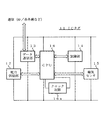
図1は、このICタグ11の構成を示す図である。
このICタグ11は、下記のユニットを内蔵する。
<< First Embodiment >>
[Description of configuration]
The first embodiment is an embodiment in which the operation mode of the IC tag is switched from the outside by moving a magnet closer to or away from the IC tag.
FIG. 1 is a diagram showing the configuration of the IC tag 11.
The IC tag 11 includes the following units.
(1)データ通信部13・・電波や赤外線などを用いてデータ通信を行う。
(2)記録部14・・通常のタグ動作に必要なプログラムやデータの他に、外部からの動作モードの切り換えに必要なプログラムやデータも記憶する。
例えば、切り換える動作モードとしては、次に挙げるものが好ましい。
『データ通信部13の動作を停止させる処理』、
『データ通信部13の動作を開始させる処理』、
『CPU16の動作を停止させる処理』、
『CPU16の動作を開始させる処理』、
『クロック回路16aからのクロック供給を停止させる処理』、
『クロック回路16aからのクロック供給を間欠的に実施させる処理』、
『クロック回路16aからのクロック供給を開始させる処理』、
『クロック回路16aの出力を低速クロックに切り換える処理』、
『クロック回路16aの出力を高速クロックに切り換える処理』、
『電力供給部17の電力供給を全部停止させる処理』、
『電力供給部17の電力供給を一部停止させる処理』、
『電力供給部17の電力供給を実行させる処理』
(3)磁気センサ15・・ICタグ11の周囲の磁気を検出するセンサ。例えば、強磁性体磁気抵抗素子(強磁性体の磁気抵抗効果を利用し、磁界強度により抵抗値が変化するセンサ)など。
(4)CPU16・・データ通信部13および記録部14を制御する。また、磁気センサ15の検出結果に応じてICタグ11の動作モードを切り換える機能も有する。
(5)クロック回路16a・・データ通信部13,CPU16などの動作クロックを生成する回路である。また、クロック周波数の切り換え機能も有する。
(6)電力供給部17・・電池などを備え、ICタグ11内に電力供給を行う。
(1) Data communication unit 13 .. Data communication is performed using radio waves or infrared rays.
(2)
For example, the following switching modes are preferable.
"Process for stopping the operation of the data communication unit 13",
“Process for starting operation of data communication unit 13”,
"Process for stopping the operation of the CPU 16",
"Process for starting the operation of the CPU 16",
"Process for stopping clock supply from clock circuit 16a",
“Process for intermittently supplying clock from clock circuit 16a”,
"Process for starting clock supply from clock circuit 16a",
“Process of switching the output of the clock circuit 16a to a low-speed clock”,
“Process for switching the output of the clock circuit 16a to a high-speed clock”,
“Process to stop all power supply of power supply unit 17”,
"Process for partially stopping the power supply of the power supply unit 17",
“Process to execute power supply of power supply unit 17”
(3) Magnetic sensor 15... Sensor that detects magnetism around the IC tag 11. For example, a ferromagnetic magnetoresistive element (a sensor that uses the magnetoresistive effect of a ferromagnetic substance and changes its resistance value depending on the magnetic field strength).
(4) CPU 16... Controls the data communication unit 13 and the
(5) Clock circuit 16a: A circuit for generating an operation clock for the data communication unit 13, the CPU 16, and the like. It also has a clock frequency switching function.
(6) A power supply unit 17... Includes a battery and supplies power to the IC tag 11.
[発明との対応関係]
以下、発明と本実施形態との対応関係について説明する。なお、ここでの対応関係は、参考のために一解釈を例示するものであり、本発明を徒らに限定するものではない。
請求項記載のデータ通信部は、データ通信部13に対応する。
請求項記載の記録部は、記録部14に対応する。
請求項記載の処理部は、CPU16の『ICタグ11を制御する機能』に対応する。
請求項記載のセンサは、磁気センサ15に対応する。
請求項記載の動作切換部は、CPU16の『磁気センサ15の検出結果に応じて、ICタグ11の動作モードを切り換える機能』に対応する。
請求項記載のタイマーは、CPU16およびクロック回路16aによる時間計測機能に対応する。
請求項記載のクロック部は、クロック回路16aに対応する。
請求項記載の電力供給部は、電力供給部17に対応する。
[Correspondence with Invention]
The correspondence relationship between the invention and this embodiment will be described below. Note that the correspondence relationship here illustrates one interpretation for reference, and does not limit the present invention.
The data communication unit described in the claims corresponds to the data communication unit 13.
The recording unit described in the claims corresponds to the
The processing unit described in the claims corresponds to the “function for controlling the IC tag 11” of the CPU 16.
The sensor recited in the claims corresponds to the magnetic sensor 15.
The operation switching unit described in the claims corresponds to the “function for switching the operation mode of the IC tag 11 according to the detection result of the magnetic sensor 15” of the CPU 16.
The timer described in the claims corresponds to a time measurement function by the CPU 16 and the clock circuit 16a.
The clock unit described in the claims corresponds to the clock circuit 16a.
The power supply unit described in the claims corresponds to the power supply unit 17.
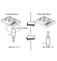
[ICタグ11に対する外部操作の方法]
次に、ICタグ11の動作モードを外部から切り換える操作方法について説明する。
図2は、この操作方法を説明する図である。
本実施形態では、磁石18をICタグ11に接近させることで、通常のタグ使用ではあり得ない程度に強い磁界をICタグ11に与える。ICタグ11内の磁気センサ15は、この強い磁界を『予め定められた外界状態』として検出し、CPU16に伝達する。
続いて、磁石18をICタグ11から遠ざけることで、ICタグ11に与えていた強い磁界を弱める。磁気センサ15は、この磁界の低下を『外界状態の変化』として検出し、CPU16に伝達する。
このように、ICタグ11に磁石18を近づけたり遠ざける操作によって、磁気センサ15の検出結果を操作し、ICタグ11に対して動作モードの切り換えを指示することができる。
[External operation method for IC tag 11]
Next, an operation method for switching the operation mode of the IC tag 11 from the outside will be described.
FIG. 2 is a diagram for explaining this operation method.
In the present embodiment, by bringing the
Subsequently, the strong magnetic field applied to the IC tag 11 is weakened by moving the
As described above, the detection result of the magnetic sensor 15 can be operated by the operation of moving the
[動作モードの選択について]
次に、ICタグ11による動作モードの切り換えシーケンスについて説明する。
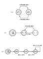
図3(A)は、動作モードの切り換え動作の一例を示す図である。
この例の場合、2つの動作モードに対応した処理1および処理2が、記録部14にプログラムとして予め記録されている。
この状態で、磁気センサ15が外界状態を検出すると、CPU16は、処理1から処理2に動作を移行する。逆に、磁気センサ15が外界状態の消滅を検出すると、CPU16は、処理2から処理1に動作を移行する。
このような動作モードの切り換え動作では、ICタグ11に与える外界状態を操作することで、処理1および処理2を交互に切り換えることができる。
[Operation mode selection]
Next, an operation mode switching sequence by the IC tag 11 will be described.
FIG. 3A is a diagram illustrating an example of the operation mode switching operation.
In this example,
In this state, when the magnetic sensor 15 detects an external state, the CPU 16 shifts the operation from the
In such an operation mode switching operation, the
図3(B)は、動作モードの切り換え動作の別の一例を示す図である。
この例の場合、ICタグ11が実行する処理が、記録部14にプログラムとして予め記録されている。この処理の終了後に磁気センサ15が外界状態を検出すると、CPU16は、この処理を再び実行する。
このように、外界状態を契機にして停止状態のICタグ11を目覚めさせ、所定の処理を、外界状態を与えるタイミングで繰り返し実行させることができる。
FIG. 3B is a diagram illustrating another example of the operation mode switching operation.
In the case of this example, the process executed by the IC tag 11 is recorded in advance in the
As described above, the IC tag 11 in the stopped state is awakened by the external state as a trigger, and the predetermined process can be repeatedly executed at the timing of giving the external state.
図3(C)は、動作モードの切り換え動作の別の一例を示す図である。
この例の場合、各種の動作モードに対応する処理1〜3が、記録部14にプログラムとして予め記録されている。処理1は、ICタグ11の製造直後に実施される処理である。
この処理1の終了後または実行中に磁気センサ15が外界状態を検出すると(検出1回目)、CPU16は処理2に動作を移行する。
この処理2の終了後または実行中に磁気センサ15が外界状態を検出すると(検出2回目)、CPU16は処理3に動作を移行する。
その後、磁気センサ15が外界状態を検出しても(検出3回目以降)、CPU16は、動作モードの切り換えを行わず、処理3を継続する。
例えば、処理1を、ICタグ11の製造時の初期化処理とする。処理2は、初期化後にICタグ11で実施するテスト処理とする。処理3は、エンドユーザーのもとで、ICタグ11が実行する処理とする。
このようにして、外界状態の有無という単純な指示でありながら、3つ以上の動作モードをシーケンシャルに切り換えることができる。
FIG. 3C is a diagram illustrating another example of the operation mode switching operation.
In this example, processes 1 to 3 corresponding to various operation modes are recorded in advance in the
When the magnetic sensor 15 detects an external environment state after the end of the
When the magnetic sensor 15 detects an external state after the end of the
Thereafter, even if the magnetic sensor 15 detects an external state (after the third detection), the CPU 16 continues the
For example, the
In this way, three or more operation modes can be sequentially switched while being a simple instruction of the presence or absence of an external state.
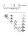
図4(A)(B)は、動作モードの切り換え動作の別の一例を示す図である。
まず、磁気センサ15が外界状態を検出すると、その時点からCPU16は、クロック回路16aを用いて、3秒間の時間範囲を計測する。CPU16は、この時間範囲における外界状態の検出回数Nspanを計数する。図4(A)には、検出回数Nspanが1回になるケースと、2回になるケースを示している。
記録部14には、この検出回数Nspanを、対応する動作モードに変換する変換ルールと、各動作モードのプログラム(処理1,2,3・・)が予め記録されている。CPU16は、計測された検出回数Nspanをこの変換ルールに従って解釈して、実行する動作モードを選択する。
図4(B)には、この変換ルールの一例に相当する状態遷移図を示す。
この変換ルールでは、初期状態から外界状態を検出すると、『検出1回』に状態遷移する。この瞬間から時間範囲(ここでは3秒間)の計測がスタートする。
この状態のまま、時間範囲が経過してタイムアウトすると、CPU16は、検出回数Nspan1回に対応する処理1を実行する。この処理1が終了すると初期状態に戻り、CPU16は、次回の動作モードの切り換え指示を待機する。
4A and 4B are diagrams illustrating another example of the operation mode switching operation.
First, when the magnetic sensor 15 detects an external state, the CPU 16 measures a time range of 3 seconds from that time using the clock circuit 16a. The CPU 16 counts the number Nspan of detections of the external state in this time range. FIG. 4A shows a case where the number of detection times Nspan is once and a case where it is twice.
In the
FIG. 4B shows a state transition diagram corresponding to an example of this conversion rule.
In this conversion rule, when an external state is detected from the initial state, the state transitions to “one detection”. From this moment, measurement of the time range (here 3 seconds) starts.
In this state, when the time range elapses and a time-out occurs, the CPU 16 executes the
なお、検出回数Nspanが1回の場合には、外界状態を誤検出している可能性があるため、処理1を『NOP』などの無効な処理にすることが好ましい。この場合、限られた時間範囲内に外界状態を2回以上検出した確実なケースのみ、動作モードの切り換えが行われるため、誤動作の発生確率を大幅に低減することができる。
一方、この時間範囲内に磁気センサ15が再び外界状態を検出すると、『検出2回』に状態遷移する。この状態のまま、時間範囲が経過してタイムアウトすると、CPU16は、検出回数Nspan2回に対応する処理2を実行する。処理2が終了すると初期状態に戻り、CPU16は、次回の動作モードの切り換え指示を待機する。
このような動作を繰り返すことにより、外界状態の有無という単純な指示でありながら、複数の動作モードをICタグ11に択一的に指示することが可能になる。
When the number of detections Nspan is 1, there is a possibility that the external state is erroneously detected. Therefore, it is preferable that the
On the other hand, when the magnetic sensor 15 detects the external state again within this time range, the state transitions to “detection twice”. In this state, when the time range elapses and the time-out occurs, the CPU 16 executes the
By repeating such an operation, a plurality of operation modes can be alternatively instructed to the IC tag 11 while being a simple instruction indicating the presence or absence of an external world state.
図5(A)(B)は、動作モードの切り換え動作の別の一例を示す図である。
まず、CPU16は、クロック回路16aを用いて、外界状態の検出時点から次回の検出時点までの時間間隔を計測する。図5(A)には、この時間間隔が3秒、1秒、2秒のケースについて示している。
記録部14には、この時間間隔を、対応する動作モードに変換する変換ルールと、各動作モードのプログラム(処理1,2,3・・)が予め記録されている。CPU16は、計測された時間間隔をこの変換ルールに従って解釈し、実行する動作モードを選択する。
図5(B)には、この変換ルールの一例に相当する状態遷移図を示す。
この変換ルールでは、最初の時間間隔が1秒の場合、CPU16は処理1を即時実行する。また、最初の時間間隔が2秒の場合、CPU16は処理2を即時実行する。一方、最初の時間間隔が3秒の場合、CPU16は『間隔3秒』に状態遷移して、次の時間間隔の計測結果を待機する。
2回目の時間間隔が1秒の場合、CPU16は処理3を実行する。また、2回目の時間間隔が2秒の場合、CPU16は処理4を実行する。一方、2回目の時間間隔が3秒の場合、CPU16は『間隔(3,3)』に状態遷移して、次の時間間隔の計測結果を待機する。
このような動作を繰り返すことにより、外界状態の有無という単純な指示でありながら、複数の動作モードをICタグ11に択一的に指示することが可能になる。
次に、ICタグ内におけるセンサ接続の態様について説明する。
5A and 5B are diagrams illustrating another example of the operation mode switching operation.
First, the CPU 16 uses the clock circuit 16a to measure the time interval from the detection time of the external world state to the next detection time point. FIG. 5A shows a case where the time interval is 3 seconds, 1 second, and 2 seconds.
In the
FIG. 5B shows a state transition diagram corresponding to an example of this conversion rule.
In this conversion rule, when the first time interval is 1 second, the CPU 16 immediately executes the
When the second time interval is 1 second, the CPU 16 executes
By repeating such an operation, a plurality of operation modes can be alternatively instructed to the IC tag 11 while being a simple instruction indicating the presence or absence of an external world state.
Next, a mode of sensor connection in the IC tag will be described.
《第2の実施形態》
図6は、ICタグ20のセンサ接続を説明する図である。
センサユニット23は、磁気センサと、磁気センサの出力を割り込み信号にレベル変換するコンパレータなどから構成される。
このセンサユニット23から出力された割り込み信号は、CPU21の割り込み端子に入力される。CPU21は、割り込み端子から割り込み信号が入力されると、HALTなどの休止状態を脱して、記録部24に記録された割り込み処理のプログラムを実施する。この割り込み処理において、外界状態の検出に同期した動作モードの実行や、動作モードの切り換え処理が実行される。
<< Second Embodiment >>
FIG. 6 is a diagram for explaining sensor connection of the IC tag 20.
The sensor unit 23 includes a magnetic sensor and a comparator that converts the output of the magnetic sensor into an interrupt signal.
The interrupt signal output from the sensor unit 23 is input to the interrupt terminal of the
このように、CPU21の割り込み機能を利用することにより、CPU21でセンサ出力を定期的に監視する必要がなくなり、CPU21の処理負担を軽減することができる。
さらに、CPU21が休止状態にあっても、割り込み機能によって、センサによる外界状態の検出に答えて動作を開始することが可能になる。したがって、CPU21やデータ通信部25を休止させた状態や、クロック供給を一部停止または全部停止させた状態から、ICタグ20を目覚めさせ、所望の動作を開始させることができる。
Thus, by using the interrupt function of the
Furthermore, even when the
《第3の実施形態》
図7は、ICタグ31のセンサ接続を説明する図である。
図7において、レギュレータ(またはDC−DCコンバータ)34は、電池32の電圧Vccを安定化して、安定化電圧Vddとして出力する。この安定化電圧Vddは、CPU35、データ通信部36、記録部37に電力供給される。
一方、センサユニット33は、電池32の電圧Vccによって作動する。このセンサユニット33は、磁気センサと、磁気センサによって外界状態を検出するたびに出力信号を反転(トグル動作)させる回路とから構成される。
このセンサユニット33の出力信号は、レギュレータ34のチップイネーブル端子に入力される。
<< Third Embodiment >>
FIG. 7 is a diagram for explaining sensor connection of the IC tag 31.
In FIG. 7, the regulator (or DC-DC converter) 34 stabilizes the voltage Vcc of the battery 32 and outputs it as a stabilized voltage Vdd. The stabilized voltage Vdd is supplied to the CPU 35, the data communication unit 36, and the
On the other hand, the sensor unit 33 is operated by the voltage Vcc of the battery 32. The sensor unit 33 includes a magnetic sensor and a circuit that inverts (toggles) an output signal each time an external state is detected by the magnetic sensor.
The output signal of the sensor unit 33 is input to the chip enable terminal of the
上述した構成により、センサユニット33による外界状態の検出/非検出に応じて、レギュレータ34のオンオフ切り換えを行うことが可能になる。
その結果、ICタグ31に所定の外界状態を与えることにより、レギュレータ34をオフ状態にして、CPU35、データ通信部36、記録部37への電力供給を停止させ、ICタグ31を省電力モードの休止状態に移行させることが可能になる。
また、この状態からICタグ31を再び外界状態を与えることにより、レギュレータ34をオン状態にして、CPU35、データ通信部36、記録部37への電力供給を再開させ、ICタグ31を通常の動作状態に移行させることが可能になる。
With the configuration described above, the
As a result, by giving a predetermined external state to the IC tag 31, the
Also, by giving the external state to the IC tag 31 again from this state, the
《第4の実施形態》
図8は、ICタグ41のセンサ接続を説明する図である。
図8において、CPU43は、I/O端子からセンサユニット46に電源電圧Vddを供給する。CPU43には、データ通信部44、および記録部45が接続される。
例えば、図3(C)に示すようなケースでは、外界状態の検出回数が上限回数を超えると、外界状態の検出が不要となる。そこで、検出回数が上限回数を上回った時点で、CPU43は、I/O端子の出力電圧をローレベルまたはハイインピーダンス状態にして、センサユニット46に対する電力供給を遮断する。
このような動作により、必要な期間のみセンサユニット46に電力を供給し、それ以外の期間はセンサユニット46への電力供給を停止させることが可能となる。その結果、ICタグ41を更に省電力化することが可能になる。特に、この構成は、電力消費の大きいフォトトランジスタをセンサとして使用する場合などに有効である。
<< Fourth Embodiment >>
FIG. 8 is a diagram for explaining sensor connection of the IC tag 41.
In FIG. 8, the CPU 43 supplies the power supply voltage Vdd to the sensor unit 46 from the I / O terminal. A data communication unit 44 and a recording unit 45 are connected to the CPU 43.
For example, in the case as shown in FIG. 3C, when the number of times of detection of the external state exceeds the upper limit number, detection of the external state becomes unnecessary. Therefore, when the number of detections exceeds the upper limit number, the CPU 43 sets the output voltage of the I / O terminal to a low level or high impedance state, and cuts off power supply to the sensor unit 46.
With such an operation, it is possible to supply power to the sensor unit 46 only during a necessary period and to stop supplying power to the sensor unit 46 during other periods. As a result, the IC tag 41 can be further reduced in power consumption. In particular, this configuration is effective when a phototransistor with high power consumption is used as a sensor.
《第5の実施形態》
図9は、ICタグ51のセンサ接続を説明する図である。
<< Fifth Embodiment >>
FIG. 9 is a diagram for explaining sensor connection of the
図9において、CPU56には、データ通信部54、および記録部55が接続される。このデータ通信部54のチップイネーブル端子には、センサユニット53の出力信号が入力される。
このような構成では、ICタグ51に与えた外界状態(磁石を近づけるなど)をセンサユニット53で検出し、電力消費の比較的大きなデータ通信部54を直にオンオフ切り換えすることが可能になる。
In FIG. 9, a
In such a configuration, it is possible to detect the external state applied to the IC tag 51 (such as approaching a magnet) by the sensor unit 53 and directly switch on and off the
《第6の実施形態》
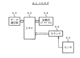
図10は、ICタグ61のセンサ接続を説明する図である。
図10において、CPU62には、データ通信部63、および記録部64が接続される。センサ65による外界状態の検出回数は、カウンタ66で計数される。カウンタ66で計数された検出回数は、CPU62に入力される。なお、CPU62からカウンタ66には、検出回数をリセットする信号が出力可能である。
このような構成では、ICタグ61に与えた外界状態(磁石を近づけるなど)をカウンタ66で計数し、この検出回数に応じて、CPU62で動作モードを切り換えることが可能になる。
<< Sixth Embodiment >>
FIG. 10 is a diagram for explaining sensor connection of the IC tag 61.
In FIG. 10, a data communication unit 63 and a recording unit 64 are connected to the CPU 62. The number of times the external state is detected by the sensor 65 is counted by the counter 66. The number of detections counted by the counter 66 is input to the CPU 62. Note that the CPU 62 can output a signal for resetting the number of detections to the counter 66.
In such a configuration, it is possible to count the external state (such as bringing a magnet closer) applied to the IC tag 61 with the counter 66 and switch the operation mode with the CPU 62 according to the number of detections.
《実施形態の補足事項》
なお、上述した実施形態では、ICタグ内に記録部を備えたケースについて説明した。しかしながら、プログラム用のメモリは、他のタグや、ICタグとネットワークで接続されるサーバ内にあってもよい。この場合は、データ通信部を介してプログラムを必要に応じてダウンロードすればよい。
<< Additional items of embodiment >>
In the above-described embodiment, the case where the recording unit is provided in the IC tag has been described. However, the program memory may be in another tag or a server connected to the IC tag via a network. In this case, what is necessary is just to download a program as needed via a data communication part.
また、上述した実施形態では、磁気センサを使用する場合について説明した。しかしながら、本発明はこれに限定されるものではない。一般的には、外部操作の可能な物理量をセンシングするセンサであればよい。例えば、電界センサ、光を検出する光センサ、静電容量センサ、圧電センサ、圧カセンサ、接触センサ、電磁波センサ、電圧センサ、リードスイッチ、受光素子としての太陽電池、温度センサ、気圧センサ、ガスセンサ、加速度センサ、歪みセンサ、超音波センサ等の音センサなどが好ましい。 In the above-described embodiment, the case where the magnetic sensor is used has been described. However, the present invention is not limited to this. In general, any sensor that senses a physical quantity that can be externally operated may be used. For example, an electric field sensor, a light sensor for detecting light, a capacitance sensor, a piezoelectric sensor, a pressure sensor, a contact sensor, an electromagnetic wave sensor, a voltage sensor, a reed switch, a solar cell as a light receiving element, a temperature sensor, an atmospheric pressure sensor, a gas sensor, Sound sensors such as an acceleration sensor, a strain sensor, and an ultrasonic sensor are preferable.
なお、ICタグの電源としては、コイン型電池、ボタン型電池等の1次電池、2次電池や太陽電池、圧電素子、熱電素子などの発電を伴う電源、キャパシタ等が好ましい。 The power source of the IC tag is preferably a primary battery such as a coin-type battery or a button-type battery, a secondary battery or a solar battery, a power source with power generation such as a piezoelectric element or a thermoelectric element, a capacitor, or the like.
また、上述した実施形態は、所定の外界状態か否かという二値検出に従って動作切り換えを行っている。しかしながら、本発明はこれに限定されるものではない。例えば、外界状態を複数設定することにより、複数種類の動作モードから一つを選択することも可能である。 In the above-described embodiment, the operation is switched according to binary detection of whether or not a predetermined external state is present. However, the present invention is not limited to this. For example, it is also possible to select one of a plurality of types of operation modes by setting a plurality of external world states.
また、物理量の値それ自体ではなく、物理量の変化方向や変化幅などの条件に基づいて外界状態を検出してもよい。例えば磁気センサであれば、磁気の変化方向や変化幅に基づいて、磁石が近づいているのか、遠ざかっているのか、磁石の移動幅といった情報を、外界状態として検出することが可能になる。 Further, the external state may be detected based on conditions such as a change direction and a change width of the physical quantity instead of the physical quantity value itself. For example, in the case of a magnetic sensor, it is possible to detect information such as whether the magnet is approaching, moving away, or the moving width of the magnet as an external state based on the direction and width of change in magnetism.
さらに、複数種類のセンサを搭載することにより、外界状態の論理組み合わせが可能になる。これらの論理(論理和や論理積や否定など)に応じて、切り換える動作モードを決定してもよい。 Furthermore, by installing a plurality of types of sensors, a logical combination of external states can be achieved. The operation mode to be switched may be determined according to these logics (logical sum, logical product, negation, etc.).
なお、上述した実施形態では、タグ形状のICタグについて説明した。しかしながら、本発明はこれに限定されるものではない。例えば、ICカードに本発明を適用してもよい。 In the above-described embodiment, the tag-shaped IC tag has been described. However, the present invention is not limited to this. For example, the present invention may be applied to an IC card.
以上説明したように、本発明は、ICタグなどに利用可能な技術である。 As described above, the present invention is a technique that can be used for an IC tag or the like.
11 ICタグ
13 データ通信部
14 記録部
15 磁気センサ
16 CPU
16a クロック回路
17 電力供給部
18 磁石
21 CPU
23 センサユニット
31 ICタグ
32 電池
33 センサユニット
34 レギュレータ
35 CPU
36 データ通信部
37 記録部
41 ICタグ
43 CPU
44 データ通信部
45 記録部
46 センサユニット
51 ICタグ
53 センサユニット
54 データ通信部
55 記録部
56 CPU
62 CPU
66 カウンタ
11 IC tag 13
16a clock circuit 17
23 Sensor unit 31 IC tag 32 Battery 33
36
44 Data communication unit 45 Recording unit 46
62 CPU
66 counter
Claims (11)
前記データ通信部を制御する処理部と
を備えたICタグであって、
前記ICタグの外界について、外部操作可能な所定の物理量をセンシングすることにより、予め定められた外界状態を検出するセンサと、
前記外界状態の検出に応じて、前記ICタグの動作モードを切り換える動作切換部と
を備えたことを特徴とするICタグ。 A data communication unit for data communication with an external device;
An IC tag comprising: a processing unit that controls the data communication unit;
A sensor that detects a predetermined external state by sensing a predetermined physical quantity that can be externally operated with respect to the external world of the IC tag,
An IC tag, comprising: an operation switching unit that switches an operation mode of the IC tag in response to detection of the external state.
前記外界状態の検出に応じて切り換える前記動作モードを記憶する記録部を備えた
ことを特徴とするICタグ。 The IC tag according to claim 1,
An IC tag, comprising: a recording unit that stores the operation mode switched according to detection of the external state.
前記外界状態の検出回数と、前記ICタグの動作モードとの対応関係を記憶する記録部を備え、
前記動作切換部は、前記外界状態の検出回数を計数し、計数された前記検出回数を前記対応関係に照合して前記ICタグの動作モードを決定する
ことを特徴とするICタグ。 The IC tag according to claim 1,
A recording unit that stores a correspondence relationship between the number of detections of the external state and the operation mode of the IC tag;
The operation switching unit counts the number of times the external state is detected, and collates the counted number of detections with the correspondence relationship to determine an operation mode of the IC tag.
前記動作切換部は、前記検出回数が所定の上限回数を上回ると、動作モードの切り換えを停止または中断する
ことを特徴とするICタグ。 The IC tag according to claim 3,
The operation switching unit stops or interrupts switching of an operation mode when the number of detection times exceeds a predetermined upper limit number.
前記外界状態の検出時点から次回の検出時点までの時間間隔を計測するタイマーと、
前記時間間隔を、前記ICタグの動作モードに変換する変換ルールを記憶する記録部とを備え、
前記動作切換部は、前記タイマーで計測された前記時間間隔を前記変換ルールに照合することにより、前記ICタグの動作モードを決定する
ことを特徴とするICタグ。 The IC tag according to claim 1,
A timer for measuring a time interval from the detection time of the external world state to the next detection time;
A recording unit for storing a conversion rule for converting the time interval into an operation mode of the IC tag,
The operation switching unit determines an operation mode of the IC tag by comparing the time interval measured by the timer with the conversion rule.
予め定められた時間範囲を検出するタイマーと、
前記時間範囲における前記外界状態の検出回数を、前記ICタグの動作モードに変換する変換ルールを記憶する記録部とを備え、
前記動作切換部は、前記時間範囲において前記外界状態の検出回数を計測し、計測した前記検出回数を前記変換ルールに照合して前記ICタグの動作モードを決定する
ことを特徴とするICタグ。 The IC tag according to claim 1,
A timer for detecting a predetermined time range;
A recording unit that stores a conversion rule for converting the number of times of detection of the external state in the time range into an operation mode of the IC tag;
The operation switching unit measures the number of detections of the external world state in the time range, and collates the measured number of detections with the conversion rule to determine an operation mode of the IC tag.
前記動作モードは、『前記データ通信部の動作を停止させる処理』、『前記データ通信部の動作を開始させる処理』、『前記処理部の動作を停止させる処理』、および『前記処理部の動作を開始させる処理』の少なくとも一つである
ことを特徴とするICタグ。 In the IC tag according to any one of claims 1 to 6,
The operation modes are “processing for stopping the operation of the data communication unit”, “processing for starting the operation of the data communication unit”, “processing for stopping the operation of the processing unit”, and “operation of the processing unit”. An IC tag, characterized in that it is at least one of the processes for starting the "."
前記処理部に動作クロックを供給するクロック部を備え、
前記動作モードは、『前記動作クロックの供給を停止させる処理』、『前記動作クロックの供給を間欠的に実施させる処理』、および『前記動作クロックを供給させる処理』の少なくとも一つである
ことを特徴とするICタグ。 In the IC tag according to any one of claims 1 to 6,
A clock unit for supplying an operation clock to the processing unit;
The operation mode is at least one of “a process for stopping the supply of the operation clock”, “a process for intermittently supplying the operation clock”, and “a process for supplying the operation clock”. Characteristic IC tag.
『データ通信に使用する高速クロック』と『前記高速クロックよりも遅い低速クロック』との切り換え機能を有するクロック部を備え、
前記動作モードは、『前記クロック部の出力を低速クロックに切り換える処理』、および『前記クロック部の出力を高速クロックに切り換える処理』の少なくとも一つである
ことを特徴とするICタグ。 In the IC tag according to any one of claims 1 to 6,
A clock unit having a switching function between "high-speed clock used for data communication" and "low-speed clock slower than the high-speed clock",
The operation mode is at least one of “a process of switching the output of the clock unit to a low-speed clock” and “a process of switching the output of the clock unit to a high-speed clock”.
前記ICタグ内に電力供給を行う電力供給部を備え、
前記動作モードは、『前記電力供給部の電力供給を全部停止させる処理』、『前記電力供給部の電力供給を一部停止させる処理』、および『前記電力供給部の電力供給を実行させる処理』の少なくとも一つである
ことを特徴とするICタグ。 In the IC tag according to any one of claims 1 to 6,
Provided with a power supply unit for supplying power in the IC tag,
The operation modes include “a process for stopping all power supply of the power supply unit”, “a process for partially stopping power supply of the power supply unit”, and “a process for executing power supply of the power supply unit”. An IC tag characterized by being at least one of the following.
前記センサは、磁気を検出する磁気センサ、電界を検出する電界センサ、光を検出する光センサ、静電容量や誘電率を検出する静電容量センサ、圧電センサ、圧力センサ、接触センサ、電磁波センサ、電圧センサ、磁界によってスイッチ切換を行うリードスイッチ、太陽電池、温度センサ、気圧センサ、ガスセンサ、加速度センサ、歪みセンサ、および音センサの少なくとも一つである
ことを特徴とするICタグ。 The IC tag according to any one of claims 1 to 10, wherein
The sensor includes a magnetic sensor that detects magnetism, an electric field sensor that detects an electric field, an optical sensor that detects light, a capacitive sensor that detects capacitance and dielectric constant, a piezoelectric sensor, a pressure sensor, a contact sensor, and an electromagnetic wave sensor. An IC tag characterized by being at least one of a voltage sensor, a reed switch that switches a switch by a magnetic field, a solar cell, a temperature sensor, an atmospheric pressure sensor, a gas sensor, an acceleration sensor, a strain sensor, and a sound sensor.
Priority Applications (1)
| Application Number | Priority Date | Filing Date | Title |
|---|---|---|---|
| JP2004111181A JP2005293485A (en) | 2004-04-05 | 2004-04-05 | Ic tag |
Applications Claiming Priority (1)
| Application Number | Priority Date | Filing Date | Title |
|---|---|---|---|
| JP2004111181A JP2005293485A (en) | 2004-04-05 | 2004-04-05 | Ic tag |
Publications (1)
| Publication Number | Publication Date |
|---|---|
| JP2005293485A true JP2005293485A (en) | 2005-10-20 |
Family
ID=35326310
Family Applications (1)
| Application Number | Title | Priority Date | Filing Date |
|---|---|---|---|
| JP2004111181A Pending JP2005293485A (en) | 2004-04-05 | 2004-04-05 | Ic tag |
Country Status (1)
| Country | Link |
|---|---|
| JP (1) | JP2005293485A (en) |
Cited By (22)
| Publication number | Priority date | Publication date | Assignee | Title |
|---|---|---|---|---|
| JP2007150435A (en) * | 2005-11-24 | 2007-06-14 | Radioware:Kk | Communication system |
| JP2007171101A (en) * | 2005-12-26 | 2007-07-05 | Nikon Vision Co Ltd | Range finder and rifle scope with ranging function |
| JP2007265082A (en) * | 2006-03-29 | 2007-10-11 | Dainippon Printing Co Ltd | Noncontact-type data carrier device equipped with noncontact-type switch, and sensor system using the noncontact-type data carrier device |
| WO2007139205A1 (en) * | 2006-05-31 | 2007-12-06 | Semiconductor Energy Laboratory Co., Ltd. | Semiconductor device and ic label, ic tag, and ic card having the same |
| JP2008086194A (en) * | 2006-08-31 | 2008-04-10 | Semiconductor Energy Lab Co Ltd | Semiconductor device and power receiving device |
| JP2009516877A (en) * | 2005-11-21 | 2009-04-23 | ヒューレット−パッカード デベロップメント カンパニー エル.ピー. | Method and apparatus for locating RFID tag |
| JP2010520522A (en) * | 2007-02-28 | 2010-06-10 | カードラボ エーピーエス | Electronic payment card, information card or ID card provided with deformation detection means |
| JP2010165315A (en) * | 2009-01-19 | 2010-07-29 | Panasonic Electric Works Co Ltd | Entrance/exit management system |
| US7911322B2 (en) | 2007-08-02 | 2011-03-22 | Sony Corporation | Information processing apparatus and method, and non-contact IC card device |
| JP2011159182A (en) * | 2010-02-02 | 2011-08-18 | Nec Access Technica Ltd | Emergency report system and emergency report method |
| US8132026B2 (en) | 2006-06-02 | 2012-03-06 | Semiconductor Energy Laboratory Co., Ltd. | Power storage device and mobile electronic device having the same |
| JP2012141227A (en) * | 2010-12-29 | 2012-07-26 | Chiba Univ | Gas sensor |
| KR101371340B1 (en) * | 2006-04-26 | 2014-03-06 | 주식회사 비즈모델라인 | Sensor Tag |
| US9022293B2 (en) | 2006-08-31 | 2015-05-05 | Semiconductor Energy Laboratory Co., Ltd. | Semiconductor device and power receiving device |
| JP2015215918A (en) * | 2009-12-22 | 2015-12-03 | メレアル ビオメトリクスMereal Biometrics | Multiple application chip card having biometric validation |
| EP3035230A1 (en) | 2014-12-19 | 2016-06-22 | Cardlab ApS | A method and an assembly for generating a magnetic field |
| WO2016136565A1 (en) * | 2015-02-27 | 2016-09-01 | 株式会社村田製作所 | Rf module and rf system |
| US10095968B2 (en) | 2014-12-19 | 2018-10-09 | Cardlabs Aps | Method and an assembly for generating a magnetic field and a method of manufacturing an assembly |
| JP2018169884A (en) * | 2017-03-30 | 2018-11-01 | 日本発條株式会社 | Portable wireless communication device, and security system using portable wireless communication device |
| US10558901B2 (en) | 2015-04-17 | 2020-02-11 | Cardlab Aps | Device for outputting a magnetic field and a method of outputting a magnetic field |
| JPWO2021100289A1 (en) * | 2019-11-22 | 2021-05-27 | ||
| JP7426860B2 (en) | 2020-03-16 | 2024-02-02 | ホシデン株式会社 | ID tag device and its driving method |
-
2004
- 2004-04-05 JP JP2004111181A patent/JP2005293485A/en active Pending
Cited By (36)
| Publication number | Priority date | Publication date | Assignee | Title |
|---|---|---|---|---|
| US9285471B2 (en) | 2005-11-21 | 2016-03-15 | Hewlett-Packard Development Company, L.P. | Method and apparatus for localization of RFID tags |
| JP2009516877A (en) * | 2005-11-21 | 2009-04-23 | ヒューレット−パッカード デベロップメント カンパニー エル.ピー. | Method and apparatus for locating RFID tag |
| JP2007150435A (en) * | 2005-11-24 | 2007-06-14 | Radioware:Kk | Communication system |
| JP2007171101A (en) * | 2005-12-26 | 2007-07-05 | Nikon Vision Co Ltd | Range finder and rifle scope with ranging function |
| JP2007265082A (en) * | 2006-03-29 | 2007-10-11 | Dainippon Printing Co Ltd | Noncontact-type data carrier device equipped with noncontact-type switch, and sensor system using the noncontact-type data carrier device |
| KR101371340B1 (en) * | 2006-04-26 | 2014-03-06 | 주식회사 비즈모델라인 | Sensor Tag |
| WO2007139205A1 (en) * | 2006-05-31 | 2007-12-06 | Semiconductor Energy Laboratory Co., Ltd. | Semiconductor device and ic label, ic tag, and ic card having the same |
| US8810375B2 (en) | 2006-05-31 | 2014-08-19 | Semiconductor Energy Laboratory Co., Ltd. | Semiconductor device and IC label, IC tag, and IC card having the same |
| US8400278B2 (en) | 2006-05-31 | 2013-03-19 | Semiconductor Energy Laboratory Co., Ltd. | Semiconductor device and IC label, IC tag, and IC card having the same |
| US8132026B2 (en) | 2006-06-02 | 2012-03-06 | Semiconductor Energy Laboratory Co., Ltd. | Power storage device and mobile electronic device having the same |
| US10256669B2 (en) | 2006-08-31 | 2019-04-09 | Semiconductor Energy Laboratory Co., Ltd. | Semiconductor device and power receiving device |
| US9022293B2 (en) | 2006-08-31 | 2015-05-05 | Semiconductor Energy Laboratory Co., Ltd. | Semiconductor device and power receiving device |
| US9531214B2 (en) | 2006-08-31 | 2016-12-27 | Semiconductor Energy Laboratory Co., Ltd. | Semiconductor device and power receiving device |
| JP2008086194A (en) * | 2006-08-31 | 2008-04-10 | Semiconductor Energy Lab Co Ltd | Semiconductor device and power receiving device |
| EP2423858B1 (en) * | 2007-02-28 | 2016-08-03 | Cardlab ApS | An electronic payment, information, or ID card with a deformation sensing means |
| JP2013242885A (en) * | 2007-02-28 | 2013-12-05 | Cardlab Aps | Electronic payment card, information card, or id card with deformation sensing means |
| JP2010520522A (en) * | 2007-02-28 | 2010-06-10 | カードラボ エーピーエス | Electronic payment card, information card or ID card provided with deformation detection means |
| JP2015149087A (en) * | 2007-02-28 | 2015-08-20 | カードラボ エーピーエスCardlab Aps | Electronic payment card, information card, or id card with deformation sensing means |
| US7911322B2 (en) | 2007-08-02 | 2011-03-22 | Sony Corporation | Information processing apparatus and method, and non-contact IC card device |
| US8742902B2 (en) | 2007-08-02 | 2014-06-03 | Sony Corporation | Information processing apparatus and method, and non-contact IC card device |
| JP2010165315A (en) * | 2009-01-19 | 2010-07-29 | Panasonic Electric Works Co Ltd | Entrance/exit management system |
| JP2018142348A (en) * | 2009-12-22 | 2018-09-13 | メレアル ビオメトリクスMereal Biometrics | Multiple application chip card having biometrics |
| JP2015215918A (en) * | 2009-12-22 | 2015-12-03 | メレアル ビオメトリクスMereal Biometrics | Multiple application chip card having biometric validation |
| JP2011159182A (en) * | 2010-02-02 | 2011-08-18 | Nec Access Technica Ltd | Emergency report system and emergency report method |
| JP2012141227A (en) * | 2010-12-29 | 2012-07-26 | Chiba Univ | Gas sensor |
| US10095968B2 (en) | 2014-12-19 | 2018-10-09 | Cardlabs Aps | Method and an assembly for generating a magnetic field and a method of manufacturing an assembly |
| US10614351B2 (en) | 2014-12-19 | 2020-04-07 | Cardlab Aps | Method and an assembly for generating a magnetic field and a method of manufacturing an assembly |
| EP3035230A1 (en) | 2014-12-19 | 2016-06-22 | Cardlab ApS | A method and an assembly for generating a magnetic field |
| JPWO2016136565A1 (en) * | 2015-02-27 | 2017-10-12 | 株式会社村田製作所 | RF module and RF system |
| US10037486B2 (en) | 2015-02-27 | 2018-07-31 | Murata Manufacturing Co., Ltd. | RF module and RF system |
| WO2016136565A1 (en) * | 2015-02-27 | 2016-09-01 | 株式会社村田製作所 | Rf module and rf system |
| US10558901B2 (en) | 2015-04-17 | 2020-02-11 | Cardlab Aps | Device for outputting a magnetic field and a method of outputting a magnetic field |
| JP2018169884A (en) * | 2017-03-30 | 2018-11-01 | 日本発條株式会社 | Portable wireless communication device, and security system using portable wireless communication device |
| JPWO2021100289A1 (en) * | 2019-11-22 | 2021-05-27 | ||
| JP7111263B2 (en) | 2019-11-22 | 2022-08-02 | 株式会社村田製作所 | RFIC module and RFID tag |
| JP7426860B2 (en) | 2020-03-16 | 2024-02-02 | ホシデン株式会社 | ID tag device and its driving method |
Similar Documents
| Publication | Publication Date | Title |
|---|---|---|
| JP2005293485A (en) | Ic tag | |
| TWI485579B (en) | Pointing member, position detection apparatus and position detection method | |
| US8604905B2 (en) | Finger biometric sensor including laterally adjacent piezoelectric transducer layer and associated methods | |
| US10482363B1 (en) | Systems and methods for detection mechanisms for magnetic cards and devices | |
| KR100225216B1 (en) | Low-power standby mode for a remote sensing device | |
| JP5935899B2 (en) | Wake-up signal generator, touch input device | |
| US20020126094A1 (en) | Input device with capacitive antenna | |
| US20140160088A1 (en) | Active stylus force sensing mechanism for generating a wakeup interrupt to the controller | |
| JP5822261B2 (en) | Terminal device, communication system, and terminal device activation method | |
| JP6593772B2 (en) | Electronic device, control method therefor, and control program | |
| CN110138372B (en) | Touch press key assembly, control circuit and electronic equipment | |
| US10488990B2 (en) | Acoustic touch device and touch judging method | |
| GB2383134A (en) | Capacitive sensing and data input device power management | |
| JP2017083479A (en) | Inertial force sensor and portable terminal using the same | |
| CN108509226A (en) | The state switching method and electronic equipment of electronic equipment | |
| US8702588B2 (en) | Play flow control apparatus and method for controlling a play flow of a sensual consumer product | |
| CN101598986A (en) | Can save the touch detection device of electrical source consumption | |
| CN104484029A (en) | Electronic device and power-saving management method thereof | |
| US20040130527A1 (en) | Input apparatus having electrostatic sensor | |
| JP5010405B2 (en) | Passive RFID sensor | |
| TWI528154B (en) | Clamshell electronic device, switching module and switching method | |
| CN111528843A (en) | Physiological information measuring method, physiological information measuring device, and electronic apparatus | |
| KR20150111043A (en) | Fingerprint authenticating apparatus detecting finger touch and operating method thereof | |
| JP5881979B2 (en) | Terminal device and communication system | |
| US11009410B2 (en) | Pressing sensor and electronic device for detecting the end of a press without error |
Legal Events
| Date | Code | Title | Description |
|---|---|---|---|
| A621 | Written request for application examination |
Free format text: JAPANESE INTERMEDIATE CODE: A621 Effective date: 20060815 |
|
| A977 | Report on retrieval |
Free format text: JAPANESE INTERMEDIATE CODE: A971007 Effective date: 20090605 |
|
| A131 | Notification of reasons for refusal |
Free format text: JAPANESE INTERMEDIATE CODE: A131 Effective date: 20090728 |
|
| A02 | Decision of refusal |
Free format text: JAPANESE INTERMEDIATE CODE: A02 Effective date: 20091124 |