JP2005277501A - Uwb antenna - Google Patents
Uwb antenna Download PDFInfo
- Publication number
- JP2005277501A JP2005277501A JP2004084021A JP2004084021A JP2005277501A JP 2005277501 A JP2005277501 A JP 2005277501A JP 2004084021 A JP2004084021 A JP 2004084021A JP 2004084021 A JP2004084021 A JP 2004084021A JP 2005277501 A JP2005277501 A JP 2005277501A
- Authority
- JP
- Japan
- Prior art keywords
- antenna
- point
- antenna device
- feeding point
- shape
- Prior art date
- Legal status (The legal status is an assumption and is not a legal conclusion. Google has not performed a legal analysis and makes no representation as to the accuracy of the status listed.)
- Pending
Links
Images


Landscapes
- Details Of Aerials (AREA)
Abstract
Description
本件発明は、超広帯域の周波数範囲で使用できるアンテナ装置に関するものである。 The present invention relates to an antenna device that can be used in an ultra-wideband frequency range.
近年、従来の無線通信に比べ、遥かに周波数スペクトルが広帯域な無線通信システムが注目されている。この超広帯域の技術は、一般に、UWB(Ultra Wide Band)と呼ばれている。従ってUWBにおいては、占有する帯域が非常に広く広帯域通信が容易に実現される。そこで多くのメーカが、PDP(Plasma Display Panel)テレビや、カメラ一体型VTR(Video Tape Recorder)、パソコンと周辺機器などのデジタル機器同士をつなぐ超高速インタフェースとして、その実用化を試みている。そしてUWBに使用されるアンテナは、これまでの他の狭帯域の無線技術と全く異なる特性であり、従来とは大幅に異なる設計法が求められる。このため、特許文献1に開示されたようなアンテナが提案されている。
しかしながら、従来のUWB用アンテナは、アンテナ形状が複雑であるため、大量生産することや、家電などの民生用途に使用できるような小型で性能のよいアンテナとして使用することが難しい。 However, since the conventional UWB antenna has a complicated antenna shape, it is difficult to mass-produce or use it as a small and high-performance antenna that can be used in consumer applications such as home appliances.
本件発明は、上記課題に鑑みなされたものである。 The present invention has been made in view of the above problems.
第一の発明は、一対のアンテナ素子からなるアンテナ装置であって、前記アンテナ素子は、尖端形状の給電点と、前記給電点からもっとも離れた尖端形状の最外点と、前記給電点と、前記最外点との中間に配置される面状領域部と、からなり、前記給電点と、前記最外点との距離が目的波の二分の一波長の長さであるアンテナ装置に関する。
第二の発明は、前記一対のアンテナ素子の形状は同一である第一の発明に記載のアンテナ装置に関する。
第三の発明は、前記アンテナ素子は、四辺形状である第一の発明又は第二の発明に記載のアンテナ装置に関する。
第四の発明は、前記四辺形状は、ひし形形状である第三の発明に記載のアンテナ装置に関する。
第五の発明は、前記給電点から入力する高周波信号の周波数の変化に対して給電点のインピーダンスの変化が中心値に対して絶対値で20%以内である第一の発明から第四の発明のいずれか一に記載のアンテナ装置に関する。
第六の発明は、前記アンテナ素子は、平面状である第一の発明から第五の発明のいずれか一に記載のアンテナ装置に関する。
第七の発明は、前記アンテナ素子は、立体状である第一の発明から第五の発明のいずれか一に記載のアンテナ装置に関する。
The first invention is an antenna device comprising a pair of antenna elements, the antenna element is a point-shaped feeding point, a point-shaped outermost point farthest from the feeding point, the feeding point, The present invention relates to an antenna device comprising a planar region portion arranged in the middle of the outermost point, wherein a distance between the feeding point and the outermost point is a length of a half wavelength of a target wave.
A second invention relates to the antenna device according to the first invention, wherein the pair of antenna elements have the same shape.
A third invention relates to the antenna device according to the first invention or the second invention, wherein the antenna element has a quadrilateral shape.
A fourth invention relates to the antenna device according to the third invention, wherein the quadrilateral shape is a rhombus shape.
According to a fifth aspect of the invention, the change in impedance at the feed point is within 20% in absolute value with respect to the center value with respect to the change in frequency of the high-frequency signal input from the feed point. The antenna device according to any one of the above.
A sixth invention relates to the antenna device according to any one of the first to fifth inventions, wherein the antenna element is planar.
A seventh invention relates to the antenna device according to any one of the first to fifth inventions, wherein the antenna element has a three-dimensional shape.
本件発明によれば、一対のアンテナ素子からなるアンテナ装置であり、アンテナ装置の給電点におけるインピーダンスの変化を低くできるので、簡単な構成で超広帯域のアンテナとして使用することができる。 According to the present invention, the antenna device is composed of a pair of antenna elements. Since the change in impedance at the feeding point of the antenna device can be reduced, the antenna device can be used as an ultra-wideband antenna with a simple configuration.
以下に本件発明の実施形態を説明する。実施形態と、請求項との関係はおおむね次のようなものである。
実施形態1は、主に、請求項1、2、3、4、6などについて説明している。
実施形態2は、主に、請求項5について説明している。
実施形態3は、主に、請求項7について説明している。
Embodiments of the present invention will be described below. The relationship between the embodiment and the claims is generally as follows.
The first embodiment mainly describes
The second embodiment mainly describes
The third embodiment mainly describes
<<実施形態1>>
以下に、実施形態1について説明する。
<<
<実施形態1の概念>
以下に、実施形態1の概念について説明する。
最近、UWBという広帯域通信が注目されている。使用周波数帯域は3.1〜10.6GHzである。主力と注目されているUWBを使用したシステムで使用周波数を区分すると、大きく分けて、(1)OFDM(Orthogonal Frequency Division Multiplexing:直交周波数分割多重)方式を用いるもの、(2)DS−SS(Direct Sequence Spectrum Spread:直接拡散)方式を用いるもの、に分類される。(1)OFDM方式では、この全周波数帯域(但し、5.2GHz帯の無線LANの周波数を除く)が使用される。(2)DS−SS方式では、さらに(2−1)3.1GHz〜5.2GHz帯の無線LANの下側が使用されるものと、(2−2)5.2GHz帯の無線LANの上側〜10.6GHzを使用するものに分類される。両方式とも、5.2GHz無線LANへの干渉が起こらないように考慮されている。
<Concept of
Below, the concept of
Recently, broadband communication called UWB has attracted attention. The used frequency band is 3.1 to 10.6 GHz. When the frequency used is divided in the system using UWB, which is attracting attention as the mainstay, (1) OFDM (Orthogonal Frequency Division Multiplexing) (2) DS-SS (Direct) It is classified into those using the Sequence Spectrum Spread (direct diffusion) method. (1) In the OFDM system, this entire frequency band (except for the frequency of the wireless LAN in the 5.2 GHz band) is used. (2) In the DS-SS system, (2-1) the lower side of the 3.1 GHz to 5.2 GHz band wireless LAN is used, and (2-2) the upper side of the 5.2 GHz band wireless LAN. It is classified into those using 10.6 GHz. Both systems are considered so as not to cause interference with the 5.2 GHz wireless LAN.
ここでUWBにおいてキーとなる技術は超広帯域アンテナである。超広帯域アンテナ設計のキー技術は、第一には、アンテナ素子の給電点近辺は高周波電流を流し、アンテナ素子の端では高周波電流を分散させるアンテナの形状、第二には、周波数変化に対してインピーダンスの変化を給電点では鈍く見えるような反共振を応用した構造とすることなどである。これらの技術を併用することにより、平面構造の小形で高利得の超広帯域アンテナが実現できる。本実施形態は、上記二つの技術を併せもったアンテナ装置に関する。 The key technology in UWB here is the ultra-wideband antenna. The key technologies for designing an ultra-wideband antenna are: first, a high-frequency current flows near the feeding point of the antenna element, the shape of the antenna that distributes the high-frequency current at the end of the antenna element, and second, the frequency change For example, a structure applying anti-resonance that makes the change in impedance look dull at the feeding point is used. By using these technologies in combination, it is possible to realize a small and high gain ultra wideband antenna having a planar structure. The present embodiment relates to an antenna device that combines the above two techniques.
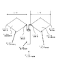
図17は、上記第一のキー技術を有したアンテナ装置1700の一例を示す図である。図17に示すアンテナ装置は、アンテナ素子1701、1702を有する。また各アンテナ素子は、給電点1704、1705を有する。アンテナ素子は、給電点からリード線を介して電子回路部1703に接続されている。一対のアンテナ素子は、三角形形状であることを特徴としている。三角形の頂点近傍が給電点となっている。図17のアンテナ素子においては、アンテナ素子の給電点と反対側(三角形の底辺側)の形状を平面的、又は立体的に大きくして、アンテナ素子に流れる高周波電流をアンテナ素子の三角形形状の底辺の両端で分散することにより、高周波電流の密度を低くする。このとき、高周波電流の観点から見ると、給電点からは、アンテナ素子の端(三角形の底辺側)の位置が分かりにくくなる。つまり、給電点からは、アンテナ装置の共振周波数が分かりにくくなる。このため、給電点からいろいろな周波数の高周波信号を入力しても、給電点付近の電流密度は高いが、端(三角形の底辺側)の部分の電流密度が低いために、電流分布の定在波が不明瞭になり、広帯域化が実現できる。なお、アンテナ素子の三角形形状は、二等辺三角形、直角二等辺三角形、不等辺三角形などが該当する。また、平面状に限定されず、立体的な構造を有していてもよい。
FIG. 17 is a diagram illustrating an example of an
<構成要件の明示>
以下に、本実施形態の構成要件を明示する。
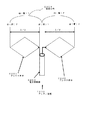
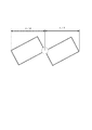
図1は、本実施形態のアンテナ装置0100の構成要件を説明するための図である。アンテナ装置は、一対のアンテナ素子0101、0102からなる。また、各アンテナ素子は、給電点0104、0105と、最外点0106、0107と、面状領域部0108、0109と、を有する。
<Clarification of configuration requirements>
In the following, the configuration requirements of this embodiment will be clarified.
FIG. 1 is a diagram for explaining the configuration requirements of the antenna device 0100 of the present embodiment. The antenna device includes a pair of antenna elements 0101 and 0102. Each antenna element has
<構成要件の説明>
以下に、本実施形態の構成要件の説明をする。
<Description of configuration requirements>
The configuration requirements of this embodiment will be described below.
<アンテナ素子>
以下に、アンテナ素子の構成要件について説明する。
<Antenna element>
Below, the component requirement of an antenna element is demonstrated.
(給電点)
「給電点」とは、リード線などにより、電子回路部0103に接続されて、電力を供給される点状の微小な領域のことをいう。給電点は、尖端形状を有する。ここで「尖端形状」とは、二本の直線又は曲線がその先端で一致することにより形成される尖った形状のことをいう。この尖端形状の有する尖端の角度は、直角に限定されず、鋭角であってもよいし、鈍角であってもよい。
(Feeding point)
The “feeding point” refers to a small dot-like region that is connected to the electronic circuit unit 0103 by a lead wire or the like and is supplied with power. The feeding point has a pointed shape. Here, the “pointed shape” refers to a pointed shape formed by matching two straight lines or curves at the tip thereof. The angle of the tip of the tip shape is not limited to a right angle, and may be an acute angle or an obtuse angle.
(最外点)
「最外点」とは、給電点からもっとも離れた点状の微小な領域のことをいう。最外点は、尖端形状を有する。ここで「尖端形状」とは、二本の直線又は曲線がその先端で一致することにより形成される尖った形状のことをいう。この尖端形状の有する尖端の角度は、直角に限定されず、鋭角であってもよいし、鈍角であってもよい。
(Outermost point)
The “outermost point” refers to a point-like minute region farthest from the feeding point. The outermost point has a pointed shape. Here, the “pointed shape” refers to a pointed shape formed by matching two straight lines or curves at the tip thereof. The angle of the tip of the tip shape is not limited to a right angle, and may be an acute angle or an obtuse angle.
(面状領域)
「面状領域部」とは、給電点と、最外点との中間に配置される面状の領域のことをいう。ここで「面」とは、板状の平面に限定されず、滑らかな曲面であってもよい。
(Surface area)
The “planar region portion” refers to a planar region disposed between the feeding point and the outermost point. Here, the “surface” is not limited to a plate-shaped plane, and may be a smooth curved surface.
(アンテナ素子)
アンテナ素子は、給電点と、最外点との距離が目的波の二分の一波長の長さを有する。また、アンテナ素子は、給電点と、最外点との距離が目的波の二分の一波長の長さに限定されず、二分の一波長の奇数倍の長さであってもよい。またアンテナ素子の形状は、一例として、四辺形状であるように形成される。さらにこの四辺形状は、一例として、ひし形形状である。ここでこのひし形形状には、正方形を含む。上記形状を有するアンテナ素子は、一例として、平面状であるように形成される。アンテナ素子は、一例として、金、銀、銅、アルミニウムなどの導体や導電性セラミックなどで構成することができる。なお、アンテナ素子を平面状に構成する場合には、その厚さを薄く構成することにより、小型のUWB機器に実装することが容易となる。アンテナ素子の厚さは、一例として、約0.1mm〜10mm程度が該当する。
(Antenna element)
In the antenna element, the distance between the feeding point and the outermost point has a length of a half wavelength of the target wave. In addition, the distance between the feeding point and the outermost point of the antenna element is not limited to the length of the half wavelength of the target wave, and may be a length that is an odd multiple of the half wavelength. The shape of the antenna element is, for example, a quadrilateral shape. Furthermore, this quadrilateral shape is a rhombus shape as an example. Here, the rhombus shape includes a square. As an example, the antenna element having the above shape is formed to be planar. As an example, the antenna element can be made of a conductor such as gold, silver, copper, or aluminum, or a conductive ceramic. When the antenna element is configured to be planar, it can be easily mounted on a small UWB device by configuring the antenna element to be thin. As an example, the thickness of the antenna element corresponds to about 0.1 mm to 10 mm.
<アンテナ装置>
以下に、アンテナ装置の構成要件について説明する。
<Antenna device>
Hereinafter, the configuration requirements of the antenna device will be described.
(アンテナ装置)
アンテナ装置は、一対のアンテナ素子からなる。この一対のアンテナ素子の形状は、一例として、同一であるように形成される。一対のアンテナ素子の各給電点は、リード線などによって、UWBの電子回路部に接続される。UWBの電子回路部は、一例として、広帯域増幅器、スイッチ、ミキサなどで構成される。
(Antenna device)
The antenna device includes a pair of antenna elements. For example, the pair of antenna elements are formed so as to have the same shape. Each feeding point of the pair of antenna elements is connected to the electronic circuit unit of the UWB by a lead wire or the like. As an example, the electronic circuit unit of the UWB includes a broadband amplifier, a switch, a mixer, and the like.
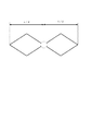
一般的に、アンテナの使用帯域幅は、給電点から入力される高周波信号の周波数の変化に対し、給電点のインピーダンスがどれくらい変化しないかで決まる。以下、図に基づいて、本実施形態のアンテナ装置がUWBアンテナとして、広帯域動作するかを説明する。 In general, the use bandwidth of an antenna is determined by how much the impedance of the feed point does not change with respect to the change of the frequency of the high-frequency signal input from the feed point. Hereinafter, based on the drawings, it will be described whether the antenna apparatus of the present embodiment operates in a wide band as a UWB antenna.
図2は、アンテナ素子の給電点より、電力を供給した場合のアンテナ装置0200の電流分布の概略を示す図である。アンテナ装置は、一対のアンテナ素子0201、0202からなる。アンテナ素子の給電点はリード線により電子回路部0203に接続されている。電子回路部より、電力が供給される。図2に示すように、アンテナ装置には、電流分布に関する定在波0204ができる。定在波は谷(節)1、谷(節)2、谷(節)3、山(腹)1、山(腹)2を有している。定在波の谷(節)1の部分に給電(電圧給電)すると、従来のように定在波の山(腹)の部分に給電する場合に比べて、給電点におけるインピーダンスの変化が鈍くなる。これは、次式より分かる。つまり、一般的に、給電点におけるインピーダンスZは、
FIG. 2 is a diagram showing an outline of the current distribution of the antenna device 0200 when power is supplied from the feeding point of the antenna element. The antenna device includes a pair of antenna elements 0201 and 0202. The feeding point of the antenna element is connected to the electronic circuit unit 0203 by a lead wire. Electric power is supplied from the electronic circuit unit. As shown in FIG. 2, the antenna device has a
Z=V/I
(V:一対のアンテナ素子の給電点間の電位差、I:アンテナ素子に流れる電流)
Z = V / I
(V: potential difference between feeding points of a pair of antenna elements, I: current flowing through the antenna elements)
で表される。ここで、従来のように電流分布の定在波の山(腹)の部分に給電(電圧給電)する場合には、給電点から入力される高周波信号の周波数の変化に対して、給電点における定在波の山(腹)の電流分布の振幅(すなわち上式のI)が変動する。すなわち、上式において、Vが一定であるとすると、給電点のインピーダンスZが変動することを意味する。しかし、本実施形態のように、給電点の電流分布の定在波の谷(節)の部分に給電(電圧給電)する場合には、給電点から入力される高周波信号の周波数の変化に対して、定在波の谷(節)の電流分布の振幅(すなわち上式のI)の変動はほとんど発生しない。つまりVが一定であるとすると、給電点のインピーダンスZがほとんど変化しない。したがって、本実施形態のアンテナ装置によれば、電流分布の定在波の谷(節)の部分に給電(電圧給電)することができるので、給電点から入力される高周波信号の周波数の変化に対して、給電点におけるインピーダンスZの変化を小さくできるため、広帯域化が実現できる。 It is represented by Here, when power is supplied (voltage power supply) to the peak (antinode) of the standing wave of the current distribution as in the past, the change in the frequency of the high-frequency signal input from the power supply point is The amplitude of the current distribution in the standing wave peak (antinode) (i.e., I in the above equation) varies. That is, in the above equation, if V is constant, it means that the impedance Z of the feeding point varies. However, as in this embodiment, when power is supplied (voltage power supply) to the portion of the standing wave trough (node) of the current distribution at the power supply point, the frequency of the high-frequency signal input from the power supply point is reduced. Thus, there is almost no fluctuation in the amplitude of the current distribution in the valley (node) of the standing wave (ie, I in the above equation). That is, assuming that V is constant, the impedance Z at the feeding point hardly changes. Therefore, according to the antenna device of the present embodiment, power can be fed (voltage fed) to the standing wave trough (node) of the current distribution, so that the frequency of the high-frequency signal input from the feeding point can be changed. On the other hand, since the change in the impedance Z at the feeding point can be reduced, a wide band can be realized.
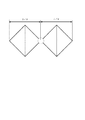
(実施例1:主に請求項2、4、6に対応)
以下に、実施例1について説明する。実施例1のアンテナ装置は、アンテナ素子の形状が平面状の正方形であり、一対のアンテナ素子の形状が同一であることを特徴とする。
図3は、実施例1のアンテナ装置の平面図あるいは底面図である。ここで、一例として、使用周波数fが、UWBの3.1〜10.6GHzであるとすると、その波長λは、光速をc=3.0×10⁸(m/s)として、次式で計算される。
(Example 1: Mainly corresponding to
Example 1 will be described below. The antenna device according to the first embodiment is characterized in that the shape of the antenna element is a planar square and the shape of the pair of antenna elements is the same.
FIG. 3 is a plan view or a bottom view of the antenna device according to the first embodiment. Here, as an example, if the operating frequency f is 3.1 to 10.6 GHz of UWB, the wavelength λ is expressed by the following equation, where the speed of light is c = 3.0 × 10 8 (m / s). Calculated.
λ=c/f
=(3.0×10⁸)/(10.6×109)
〜(3.0×10⁸)/(3.1×109)
=約28.3〜96.8(mm)
λ = c / f
= (3.0 × 10 8 ) / (10.6 × 10 9 )
~ (3.0 × 10 8 ) / (3.1 × 10 9 )
= About 28.3-96.8 (mm)
となる。よってアンテナ素子は、一辺の長さが約10.2〜34.2mm((λ/2)/√2より)の正方形となる。 It becomes. Therefore, the antenna element is a square having a side length of about 10.2 to 34.2 mm (from (λ / 2) / √2).
図4は、実施例1のアンテナ装置の正面図あるいは背面図である。
図5は、実施例1のアンテナ装置の右側面図あるいは左側面図である。
図6は、実施例1のアンテナ装置の斜視図である。
FIG. 4 is a front view or a rear view of the antenna device according to the first embodiment.
FIG. 5 is a right side view or a left side view of the antenna device according to the first embodiment.
FIG. 6 is a perspective view of the antenna device according to the first embodiment.
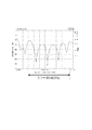
図7は、本実施形態のアンテナ装置を使用した場合の、Return Loss(電圧リターンロス)あるいはVSWR(Voltage Standing Wave Ratio:電圧定在波比)と、UWBの使用周波数3.1〜10.6GHzとの関係を、シミュレーションにより求めたものである。ここで左側の縦軸はReturn Loss(dB)を、右側の縦軸はVSWRを、横軸は使用周波数(GHz)をそれぞれ示している。一般的に、アンテナのReturn Lossが約−10dB以下、VSWRで換算すると約2.0以下であれば、品質を落とすことなく使用できる。またReturn Loss、VSWRはそれぞれ次式で定義される。 FIG. 7 shows a return loss (voltage return loss) or VSWR (Voltage Standing Wave Ratio) when using the antenna apparatus of this embodiment, and a UWB use frequency of 3.1 to 10.6 GHz. Is obtained by simulation. Here, the left vertical axis represents Return Loss (dB), the right vertical axis represents VSWR, and the horizontal axis represents the operating frequency (GHz). In general, if the return loss of the antenna is about −10 dB or less and converted to VSWR of about 2.0 or less, the antenna can be used without degrading the quality. Return Loss and VSWR are defined by the following equations, respectively.
Return Loss=20log(Vr/Vf)(dB)
(Vf:進行波電圧、Vf:反射波電圧)
Return Loss = 20 log (Vr / Vf) (dB)
(Vf: traveling wave voltage, Vf: reflected wave voltage)
VSWR=(1+|ρ|)/(1−|ρ|)
(ρ=Vr/Vf:電圧反射係数)
VSWR = (1+ | ρ |) / (1− | ρ |)
(Ρ = Vr / Vf: voltage reflection coefficient)
図7においては、UWBの使用周波数3.1〜10.6GHzに亙って、本実施形態のアンテナ装置のReturn Lossが約−10dB以下、VSWRで換算すると約2.0以下となっていることが分かる。なお、図7においては、UWBの使用周波数3.1〜10.6GHzの中心周波数である6.85GHzとして、波長λを算出し、アンテナ素子の一辺の長さを、約15.5mmとして計算している。 In FIG. 7, the Return Loss of the antenna device of the present embodiment is about −10 dB or less and about 2.0 or less in terms of VSWR, over the UWB use frequency of 3.1 to 10.6 GHz. I understand. In FIG. 7, the wavelength λ is calculated as 6.85 GHz, which is the center frequency of the UWB operating frequency 3.1 to 10.6 GHz, and the length of one side of the antenna element is calculated as approximately 15.5 mm. ing.
(実施例2:主に請求項1に対応)
以下に、実施例2について説明する。実施例2のアンテナ装置は、一対のアンテナ素子の形状が同一でないことを特徴とする。
図8は、実施例2のアンテナ装置の一例を示す平面図あるいは底面図である。図8に示すアンテナ装置は、右側のアンテナ素子の形状が正方形であり、左側のアンテナ素子の形状が、正方形の四つの角のうち、給電点と最外点以外の二つの角が丸みを帯びていることを特徴としている。
(Example 2: Mainly corresponding to claim 1)
Example 2 will be described below. The antenna device according to the second embodiment is characterized in that the shapes of the pair of antenna elements are not the same.
FIG. 8 is a plan view or a bottom view illustrating an example of the antenna device according to the second embodiment. In the antenna device shown in FIG. 8, the shape of the antenna element on the right side is a square, and the shape of the antenna element on the left side is rounded at the two corners of the square except for the feeding point and the outermost point. It is characterized by having.
(実施例3:主に請求項2に対応)
以下に、実施例3について説明する。実施例3のアンテナ装置は、一対のアンテナ素子の形状が同一であることを特徴とする。
図9は、実施例3のアンテナ装置の一例を示す平面図あるいは底面図である。図9に示すアンテナ装置は、一対のアンテナ素子の形状が、正方形の四つの角のうち、給電点と最外点以外の二つの角が丸みを帯びていることを特徴としている。
(Example 3: mainly corresponding to claim 2)
Example 3 will be described below. The antenna device according to the third embodiment is characterized in that the shape of the pair of antenna elements is the same.
FIG. 9 is a plan view or a bottom view illustrating an example of the antenna device according to the third embodiment. The antenna device shown in FIG. 9 is characterized in that the shape of the pair of antenna elements is rounded at two corners other than the feeding point and the outermost point among the four corners of the square.
(実施例4:主に請求項2、3に対応)
以下に、実施例4について説明する。実施例4のアンテナ装置は、アンテナ素子は、四辺形状であることを特徴とする。
図10は、実施例4のアンテナ装置の一例を示す平面図あるいは底面図である。図10に示すアンテナ装置は、一対のアンテナ素子の形状が、長方形であることを特徴としている。なお、一対のアンテナ形状が異なっていてもよい。
(Example 4: mainly corresponding to
Example 4 will be described below. The antenna device according to the fourth embodiment is characterized in that the antenna element has a quadrilateral shape.
FIG. 10 is a plan view or a bottom view illustrating an example of the antenna device according to the fourth embodiment. The antenna device shown in FIG. 10 is characterized in that the shape of the pair of antenna elements is a rectangle. Note that the shape of the pair of antennas may be different.
(実施例5:主に請求項2、4に対応)
以下に、実施例5について説明する。実施例5のアンテナ装置は、アンテナ素子は、ひし形形状であることを特徴とする。
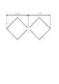
図11は、実施例5のアンテナ装置の一例を示す平面図あるいは底面図である。図11に示すアンテナ装置は、一対のアンテナ素子の形状が、ひし形であることを特徴としている。なお、一対のアンテナ形状が異なっていてもよい。
(Example 5: mainly corresponding to
Example 5 will be described below. The antenna device according to the fifth embodiment is characterized in that the antenna element has a rhombus shape.
FIG. 11 is a plan view or a bottom view illustrating an example of the antenna device according to the fifth embodiment. The antenna device shown in FIG. 11 is characterized in that the shape of the pair of antenna elements is a rhombus. Note that the shape of the pair of antennas may be different.
<実施形態1の効果の簡単な説明>
<Simple explanation of effect of
本実施形態のアンテナ装置によれば、給電点から入力される高周波信号の周波数の変化に対して、給電点におけるインピーダンスの変化を小さくできるため、広帯域化が実現できる。 According to the antenna device of the present embodiment, since the change in impedance at the feed point can be reduced with respect to the change in the frequency of the high-frequency signal input from the feed point, a wide band can be realized.
<<実施形態2>>
以下に、実施形態2について説明する。
<<
The second embodiment will be described below.
<実施形態2の概念>
以下に、実施形態2の概念について説明する。
本実施形態のアンテナ装置は、給電点から入力する高周波信号の周波数の変化に対して給電点のインピーダンスの変化が中心値に対して絶対値で20%以内である実施形態1に記載のアンテナ装置に関する。
図12は、UWBの使用周波数(横軸)と、給電点のインピーダンス(縦軸)の関係の一例を示す図である。給電点から入力する高周波信号の周波数3.1〜10.6GHzの中心周波数である6.85GHzに対して給電点インピーダンスが50Ωとした場合には、本実施形態のアンテナ装置は、45〜55Ωとなるように構成される。
<Concept of
Below, the concept of
The antenna apparatus according to the first embodiment is such that the change in impedance at the feed point is within 20% in absolute value with respect to the center value with respect to the change in the frequency of the high-frequency signal input from the feed point. About.
FIG. 12 is a diagram illustrating an example of the relationship between the UWB use frequency (horizontal axis) and the impedance of the feeding point (vertical axis). When the feed point impedance is 50Ω with respect to 6.85 GHz which is the center frequency of the frequency 3.1 to 10.6 GHz of the high frequency signal input from the feed point, the antenna device of the present embodiment is 45 to 55Ω. It is comprised so that it may become.
<実施形態2の効果の簡単な説明>
<Simple explanation of effect of
本実施形態のアンテナ装置によれば、給電点のインピーダンスの変化が中心値に対して絶対値で20%以内にすることにより、UWBの使用領域に対して、高品質のアンテナ装置を提供することができる。 According to the antenna device of the present embodiment, a high-quality antenna device is provided for a UWB usage region by making the change in impedance at the feeding point within 20% in absolute value with respect to the center value. Can do.
<<実施形態3>>
<<
<実施形態3の概念>
以下に、実施形態3の概念について説明する。
本実施形態のアンテナ装置は、アンテナ素子は、立体状である実施形態1又は2に記載のアンテナ装置に関する。
<Concept of
The concept of
The antenna device according to the present embodiment relates to the antenna device according to the first or second embodiment, in which the antenna element has a three-dimensional shape.
(実施例6)
以下に、実施例6について説明する。実施例6のアンテナ装置は、立体状であることを特徴とする。
図13は、実施例6のアンテナ装置の平面図あるいは底面図である。
図14は、実施例6のアンテナ装置の正面図あるいは背面図である。
図15は、実施例6のアンテナ装置の右側面図あるいは左側面図である。
図16は、実施例6のアンテナ装置の斜視図である。
(Example 6)
Example 6 will be described below. The antenna device according to the sixth embodiment has a three-dimensional shape.
FIG. 13 is a plan view or a bottom view of the antenna device according to the sixth embodiment.
FIG. 14 is a front view or a rear view of the antenna device according to the sixth embodiment.
FIG. 15 is a right side view or a left side view of the antenna device according to the sixth embodiment.
FIG. 16 is a perspective view of the antenna device according to the sixth embodiment.
<実施形態3の効果の簡単な説明>
<Simple explanation of effect of
本実施形態のアンテナ装置によれば、給電点から入力される高周波信号の周波数の変化に対して、給電点におけるインピーダンスの変化を小さくできるため、広帯域化が実現できる。 According to the antenna device of the present embodiment, since the change in impedance at the feed point can be reduced with respect to the change in the frequency of the high-frequency signal input from the feed point, a wide band can be realized.
本件発明は、家電などの民生用途に使用できるような小型で性能のよいUWBアンテナとして使用することができる。 The present invention can be used as a small and high-performance UWB antenna that can be used in consumer applications such as home appliances.
0100 アンテナ装置
0101 アンテナ素子
0102 アンテナ素子
0103 電子回路部
0104 給電点
0105 給電点
0106 最外点
0107 最外点
0108 面状領域部
0109 面状領域部
0100 Antenna device 0101 Antenna element 0102 Antenna element 0103
Claims (7)
前記アンテナ素子は、
尖端形状の給電点と、
前記給電点からもっとも離れた尖端形状の最外点と、
前記給電点と、前記最外点との中間に配置される面状領域部と、
からなり、
前記給電点と、前記最外点との距離が目的波の二分の一波長の長さであるアンテナ装置。 An antenna device comprising a pair of antenna elements,
The antenna element is
A point-shaped feeding point;
A pointed outermost point furthest away from the feed point;
A planar region disposed between the feeding point and the outermost point;
Consists of
An antenna apparatus, wherein a distance between the feeding point and the outermost point is a length of a half wavelength of a target wave.
Priority Applications (1)
| Application Number | Priority Date | Filing Date | Title |
|---|---|---|---|
| JP2004084021A JP2005277501A (en) | 2004-03-23 | 2004-03-23 | Uwb antenna |
Applications Claiming Priority (1)
| Application Number | Priority Date | Filing Date | Title |
|---|---|---|---|
| JP2004084021A JP2005277501A (en) | 2004-03-23 | 2004-03-23 | Uwb antenna |
Publications (1)
| Publication Number | Publication Date |
|---|---|
| JP2005277501A true JP2005277501A (en) | 2005-10-06 |
Family
ID=35176739
Family Applications (1)
| Application Number | Title | Priority Date | Filing Date |
|---|---|---|---|
| JP2004084021A Pending JP2005277501A (en) | 2004-03-23 | 2004-03-23 | Uwb antenna |
Country Status (1)
| Country | Link |
|---|---|
| JP (1) | JP2005277501A (en) |
Cited By (4)
| Publication number | Priority date | Publication date | Assignee | Title |
|---|---|---|---|---|
| JPWO2007055028A1 (en) * | 2005-11-14 | 2009-04-30 | アンリツ株式会社 | Linearly polarized antenna and radar apparatus using the same |
| WO2010044262A1 (en) | 2008-10-17 | 2010-04-22 | 三菱電線工業株式会社 | Wideband antenna |
| CN104377434A (en) * | 2013-08-13 | 2015-02-25 | Ace技术株式会社 | Wideband base station antenna radiator |
| US11417955B2 (en) | 2018-08-10 | 2022-08-16 | Morita Tech Co., Ltd. | Antenna device |
-
2004
- 2004-03-23 JP JP2004084021A patent/JP2005277501A/en active Pending
Cited By (7)
| Publication number | Priority date | Publication date | Assignee | Title |
|---|---|---|---|---|
| JPWO2007055028A1 (en) * | 2005-11-14 | 2009-04-30 | アンリツ株式会社 | Linearly polarized antenna and radar apparatus using the same |
| JP4681614B2 (en) * | 2005-11-14 | 2011-05-11 | アンリツ株式会社 | Linearly polarized antenna and radar apparatus using the same |
| WO2010044262A1 (en) | 2008-10-17 | 2010-04-22 | 三菱電線工業株式会社 | Wideband antenna |
| US8599079B2 (en) | 2008-10-17 | 2013-12-03 | Mitsubishi Cable Industries, Ltd. | Wideband antenna |
| CN104377434A (en) * | 2013-08-13 | 2015-02-25 | Ace技术株式会社 | Wideband base station antenna radiator |
| CN104377434B (en) * | 2013-08-13 | 2017-12-05 | Ace技术株式会社 | Wide bandwidth base station antenna radiant body |
| US11417955B2 (en) | 2018-08-10 | 2022-08-16 | Morita Tech Co., Ltd. | Antenna device |
Similar Documents
| Publication | Publication Date | Title |
|---|---|---|
| JP4949469B2 (en) | Embedded multimode antenna architecture for wireless devices | |
| KR101101215B1 (en) | Antenna device and communication apparatus employing same | |
| CN107437661A (en) | Antenna and mobile terminal | |
| US20030231139A1 (en) | Wide band antenna | |
| CN109301472A (en) | Double frequency-band millimeter wave antenna | |
| TW200830628A (en) | Plane antenna | |
| TW201117472A (en) | Printed dual-band antenna for electronic device | |
| TW200840138A (en) | Ultra-wide band antenna and plug-and-play device using the same | |
| JPWO2009125492A1 (en) | Power distributor | |
| TW201830771A (en) | Split ring resonator (srr) antenna | |
| KR101915388B1 (en) | Antenna device | |
| US7612733B2 (en) | Transition region for use with an antenna-integrated electron tunneling device and method | |
| CN104966903B (en) | A kind of suspension micro-strip antenna array and its antenna for 60GHz millimetre-wave attenuators | |
| JP2005277501A (en) | Uwb antenna | |
| JP2005252526A (en) | Antenna system, electronic equipment using the same, and radio communication card | |
| US20070030197A1 (en) | Antenna Structure | |
| TWM319527U (en) | Planar antenna | |
| CN110581356A (en) | Novel coplanar waveguide dual-frequency antenna | |
| CN106058442B (en) | A kind of antenna | |
| JP2021019247A (en) | Antenna device | |
| JP4965880B2 (en) | Antenna device | |
| JP2000114801A (en) | Connection structure for high frequency transmission line | |
| CN103904418A (en) | Omnidirectional terminal antenna | |
| CN105322303B (en) | Antenna assembly | |
| JP2005286997A (en) | Antenna device, electronic apparatus using the same and radio communication card |
Legal Events
| Date | Code | Title | Description |
|---|---|---|---|
| A711 | Notification of change in applicant |
Effective date: 20060906 Free format text: JAPANESE INTERMEDIATE CODE: A711 |
|
| RD02 | Notification of acceptance of power of attorney |
Free format text: JAPANESE INTERMEDIATE CODE: A7422 Effective date: 20060920 |
|
| A521 | Written amendment |
Free format text: JAPANESE INTERMEDIATE CODE: A821 Effective date: 20060907 |