JP2005251982A - Silicon film forming method, manufacturing method of device using the same, and manufacturing method using manufacturing method of the same device - Google Patents
Silicon film forming method, manufacturing method of device using the same, and manufacturing method using manufacturing method of the same device Download PDFInfo
- Publication number
- JP2005251982A JP2005251982A JP2004060466A JP2004060466A JP2005251982A JP 2005251982 A JP2005251982 A JP 2005251982A JP 2004060466 A JP2004060466 A JP 2004060466A JP 2004060466 A JP2004060466 A JP 2004060466A JP 2005251982 A JP2005251982 A JP 2005251982A
- Authority
- JP
- Japan
- Prior art keywords
- forming
- silicon film
- silicon material
- heat treatment
- liquid silicon
- Prior art date
- Legal status (The legal status is an assumption and is not a legal conclusion. Google has not performed a legal analysis and makes no representation as to the accuracy of the status listed.)
- Pending
Links
Images

Landscapes
- Liquid Deposition Of Substances Of Which Semiconductor Devices Are Composed (AREA)
- Thin Film Transistor (AREA)
- Recrystallisation Techniques (AREA)
Abstract
Description
本発明は、シリコン膜の形成方法、当該シリコン膜の形成方法を用いた集積回路、薄膜トランジスタ、光電変換装置等のデバイスの製造方法及び当該デバイスの製造方法を用いたディスプレイ等の電気光学機器に関する。 The present invention relates to a silicon film forming method, an integrated circuit using the silicon film forming method, a method for manufacturing a device such as a thin film transistor and a photoelectric conversion device, and an electro-optical device such as a display using the device manufacturing method.
集積回路や薄膜トランジスタ等に応用されるシリコン薄膜(アモルファスシリコン膜やポリシリコン膜)のパターニングは、CVD(Chemical Vapor Deposition)法等の真空プロセスにより基板の全面にシリコン膜を形成した後、フォトリソグラフィーにより不要部分を除去するといったプロセスで行なわれるのが一般的である。しかし、この方法では、大掛かりな装置が必要である、原料の使用効率が悪い、原料が気体であるため扱いにくい、大量の廃棄物が発生する、等の問題を有していた。 Patterning of a silicon thin film (amorphous silicon film or polysilicon film) applied to an integrated circuit or a thin film transistor is performed by forming a silicon film on the entire surface of the substrate by a vacuum process such as a CVD (Chemical Vapor Deposition) method, and then performing photolithography. The process is generally performed by removing unnecessary portions. However, this method has problems such as requiring a large-scale device, poor use efficiency of the raw material, difficulty in handling because the raw material is gas, and generation of a large amount of waste.
また、近年ディスプレイが大画面化するに伴って、基板も1m四方をゆうに越える大きさになってきており、コスト面もさることながら、そのような巨大基板に均一にシリコン成膜を行う事が困難であるという技術的な課題も浮上するようになってきた。 In recent years, with the increase in the size of displays, the size of the substrate has exceeded 1 m square. Silicon film can be uniformly formed on such a huge substrate while reducing the cost. The technical problem that this is difficult has also surfaced.
このような従来方法に対して、近年、液体状のシラン化合物や高次シラン化合物又はその溶液等の液体シリコン材料を基板に塗布し、加熱又はUVの照射によってシリコン膜を形成する方法が提案されている(例えば、特開2003−115532号公報:特許文献1、特開2003−124486号公報:特許文献2、特開2003−133306号公報:特許文献3、特開2003−171556号公報:特許文献4等)。この方法によれば、原料が液体であるため扱い易く、大型の装置を必要としないため、低コストでシリコン膜を作製することができる。 In contrast to such conventional methods, in recent years, a method has been proposed in which a liquid silicon material such as a liquid silane compound, a higher order silane compound, or a solution thereof is applied to a substrate, and a silicon film is formed by heating or UV irradiation. (For example, JP 2003-115532 A: Patent Document 1, JP 2003-124486 A: Patent Document 2, JP 2003-133306 A: Patent Document 3, JP 2003-171556 A: Patent. Reference 4). According to this method, since the raw material is a liquid, it is easy to handle and a large-sized apparatus is not required, so that a silicon film can be manufactured at low cost.
また、特開2001−179167号公報には、溶液シリコン材料をインクジェットなどの手法により直接パターニングしてシリコン膜を作製することができるようになり、これによってフォトリソグラフィーによる工数、材料の無駄を省くことができる旨が開示されている(特許文献5)。
上記の先行技術ではインクジェット法やその他の液滴パターニング方法を用いてシリコン膜を直接パターニングすることができるが、例えばインクジェット法の精度は数十ミクロン程度であり、ミクロンオーダー、サブミクロンオーダーの微細なシリコンパターンを形成することは困難である。 In the above prior art, the silicon film can be directly patterned by using the ink jet method or other droplet patterning methods. It is difficult to form a silicon pattern.
また、SAM膜(自己組織化単分子膜:self-assembled monolayer)を用いた撥液/親液パターンにより微細化を行うこともできるが、SAM膜は紫外線(以下「UV」と称する)光に対する感度が低いため、パターニングには非常に高い強度のランプが必要となり、コスト、時間的に不利である。また、得られるSAM膜のパターンもサブミクロンレベルで微細であるとは言いがたい。 Further, the SAM film can be miniaturized by a lyophobic / lyophilic pattern using a SAM film (self-assembled monolayer). However, the SAM film is resistant to ultraviolet (hereinafter referred to as “UV”) light. Due to the low sensitivity, patterning requires a very high intensity lamp, which is disadvantageous in terms of cost and time. Also, it is difficult to say that the pattern of the obtained SAM film is fine at the submicron level.
また、液体シリコン材料の熱分解を起こさせるには300℃以上の温度で加熱する必要があるために、通常の耐熱温度が180℃程度であるフォトレジストは高温に耐えることができず、レジストパターンの形状が崩れたり、フォトレジストが熱分解してしまうため、上記液体シリコン材料を用いたシリコン成膜に用いる事には問題があった。 In addition, since it is necessary to heat at a temperature of 300 ° C. or higher in order to cause thermal decomposition of the liquid silicon material, a photoresist having a normal heat-resistant temperature of about 180 ° C. cannot withstand high temperatures. As a result, the photoresist is deformed and the photoresist is thermally decomposed, so that there is a problem in using it for silicon film formation using the liquid silicon material.
そこで、本発明は、耐熱性に優れたフォトレジストを用い、微細なシリコン膜のパターニングを行うことができるシリコン膜の形成方法を提供することを目的とする。 Therefore, an object of the present invention is to provide a method for forming a silicon film, which can perform patterning of a fine silicon film using a photoresist having excellent heat resistance.
本発明の発明者等は上記課題を解決するために鋭意検討を行った結果、ある条件下でフォトレジストを処理すると耐熱性が向上し、液体シリコン材料を熱分解する温度下においてもフォトレジストの変形又は分解が起こらない硬化フォトレジストが得られるという知見を得た。本発明はこの知見に基づくものであり、基体上にレジストパターンを形成し、凹部を形成する工程と、前記凹部に液体シリコン材料を塗布する工程と、前記レジストパターン及び塗布された前記液体シリコン材料に対して、光処理及び第1熱処理を行う工程と、前記液体シリコン材料に対して、第2熱処理を行う工程と、を含む、シリコン膜の形成方法(以下「第1発明」ということがある)を提供するものである。 The inventors of the present invention have intensively studied to solve the above-mentioned problems, and as a result, when the photoresist is processed under certain conditions, the heat resistance is improved, and even at a temperature at which the liquid silicon material is thermally decomposed, It was found that a cured photoresist that does not deform or decompose is obtained. The present invention is based on this knowledge, a step of forming a resist pattern on a substrate and forming a recess, a step of applying a liquid silicon material to the recess, the resist pattern and the applied liquid silicon material In contrast, there may be a silicon film forming method (hereinafter referred to as “first invention”), which includes a step of performing a light treatment and a first heat treatment, and a step of performing a second heat treatment on the liquid silicon material. ).
これにより、耐熱性に優れたレジストパターンを形成することができ、液体シリコン材料を熱分解する温度においてもそのレジストパターンが変化することがないため、フォトリソグラフィーの精度(サブミクロンレベル)にまで微細なシリコン膜のパターニングを行うことができる。なお、上記の方法で得られたレジストパターンは、アセトン洗浄やアッシング等の通常のレジスト剥離処理によって容易に除去することができる。 As a result, a resist pattern with excellent heat resistance can be formed, and the resist pattern does not change even at the temperature at which the liquid silicon material is thermally decomposed. It is possible to pattern the silicon film. The resist pattern obtained by the above method can be easily removed by a normal resist stripping process such as acetone cleaning or ashing.
本発明の好ましい実施形態は以下のとおりである。前記光処理により、前記液体シリコン材料の光重合を行うことが好ましい。前記第1熱処理により、前記液体シリコン材料の溶媒を除去することが好ましい。前記光処理及び第1熱処理は、圧力が10-9〜100Torr、該光処理の光の波長が170〜600nm及び該第1熱処理の温度が20〜150℃を含む条件下で行われることが好ましい。前記第2熱処理は、300〜450℃で行われることが好ましい。前記光処理に用いられる光源は、高圧水銀灯、低圧水銀灯、エキシマランプ、エキシマレーザのいずれかから選択されることが好ましい。前記液体シリコン材料が、シラン化合物及び/又は高次シランを含むことが好ましい。前記液体シリコン材料の塗布は、液滴吐出法により行われることが好ましい。 Preferred embodiments of the present invention are as follows. It is preferable to perform photopolymerization of the liquid silicon material by the light treatment. It is preferable to remove the solvent of the liquid silicon material by the first heat treatment. The light treatment and the first heat treatment are preferably performed under conditions including a pressure of 10 −9 to 100 Torr, a wavelength of light of the light treatment of 170 to 600 nm, and a temperature of the first heat treatment of 20 to 150 ° C. . The second heat treatment is preferably performed at 300 to 450 ° C. The light source used for the light treatment is preferably selected from any one of a high pressure mercury lamp, a low pressure mercury lamp, an excimer lamp, and an excimer laser. The liquid silicon material preferably contains a silane compound and / or a higher order silane. The liquid silicon material is preferably applied by a droplet discharge method.
また、本発明は、基体上にレジストパターンを形成し、凹部を形成する工程と、前記レジストパターンに対して、光処理及び第1熱処理を行う工程と、前記凹部に液体シリコン材料を塗布する工程と、前記液体シリコン材料に対して、第2熱処理を行う工程と、を含むシリコン膜の形成方法(以下「第2発明」ということがある)を提供するものである。 The present invention also includes a step of forming a resist pattern on a substrate and forming a recess, a step of performing a light treatment and a first heat treatment on the resist pattern, and a step of applying a liquid silicon material to the recess. And a step of performing a second heat treatment on the liquid silicon material. The present invention provides a method for forming a silicon film (hereinafter sometimes referred to as a “second invention”).
また、本発明は、上記のシリコン膜の形成方法を使用するデバイスの製造方法(以下「第3発明」ということがある)を提供するものである。更に、当該デバイスの製造方法を使用する電気光学機器の製造法(以下「第4発明」ということがある)を提供するものである。上記のシリコン膜の形成方法を使用することにより低コストな液体シリコン材料を用いてサブミクロンレベルにまで微細なシリコン膜のパターニングを行うことができるため、コスト、性能ともに優れたデバイス並びに電気光学機器を製造することができる。 The present invention also provides a device manufacturing method (hereinafter sometimes referred to as “third invention”) using the above-described silicon film forming method. Furthermore, the present invention provides a method for manufacturing an electro-optical device (hereinafter sometimes referred to as “fourth invention”) using the device manufacturing method. By using the silicon film formation method described above, it is possible to pattern a fine silicon film down to the submicron level using a low-cost liquid silicon material. Can be manufactured.
本発明によれば、液体シリコン材料を熱分解させる温度(例えば300〜450℃)においてもフォトレジストが変形又は分解することなく、レジストパターンが維持されるため、サブミクロンレベルにまで微細なシリコン膜のパターニングを行うことができる。 According to the present invention, the resist pattern is maintained without deforming or decomposing the photoresist even at a temperature (for example, 300 to 450 ° C.) at which the liquid silicon material is thermally decomposed. Can be patterned.
以下、本発明に係るシリコン膜の形成方法等を、その好ましい実施形態に基づいて詳細に説明する。 Hereinafter, a silicon film forming method and the like according to the present invention will be described in detail based on preferred embodiments thereof.
[第1発明]
本発明は、既述のとおり、基体上にレジストパターンを形成し、凹部を形成する工程と、前記凹部に液体シリコン材料を塗布する工程と、前記レジストパターン及び塗布された前記液体シリコン材料に対して、光処理及び第1熱処理を行う工程と、前記液体シリコン材料に対して、第2熱処理を行う工程と、を含むことを特徴とする。
[First invention]
As described above, the present invention includes a step of forming a resist pattern on a substrate and forming a recess, a step of applying a liquid silicon material to the recess, and the resist pattern and the applied liquid silicon material. And a step of performing a light treatment and a first heat treatment, and a step of performing a second heat treatment on the liquid silicon material.
先ず、基体上にレジストパターンを形成し、凹部を形成する工程について説明する。フォトレジストは、感光剤、樹脂、溶剤を含む一般的な感光性樹脂を用いることができ、可視光線やUVの光源用のノボラック型、エキシマレーザ光源用の化学増幅型のいずれのタイプも使用することができる。また、光が照射された部分が残るネガ型、光が照射された部分が除去されるポジ型のいずれでもよい。 First, a process of forming a resist pattern on a substrate and forming a recess will be described. As the photoresist, a general photosensitive resin containing a photosensitive agent, a resin, and a solvent can be used, and any type of a novolak type for a visible light or UV light source or a chemical amplification type for an excimer laser light source is used. be able to. Moreover, either a negative type in which a portion irradiated with light remains or a positive type in which a portion irradiated with light is removed may be used.
本発明において「基体」とは、特に限定されないが、通常の石英、ホウ珪酸ガラス、ソーダガラスの他、ITOなどの透明電極、金、銀、銅、ニッケル、チタン、アルミニウム、タングステンなどの金属基板、さらにこれらの金属を表面に有するガラス、プラスチック基板などのほか、これらの基板の表面上に形成されたシリコン膜や金属膜等も含まれる。 In the present invention, the “substrate” is not particularly limited, but other than ordinary quartz, borosilicate glass, soda glass, transparent electrodes such as ITO, metal substrates such as gold, silver, copper, nickel, titanium, aluminum, tungsten, etc. In addition to glass and plastic substrates having these metals on the surface, silicon films and metal films formed on the surfaces of these substrates are also included.
レジストパターンは、通常用いられるフォトリソグラフィ技術により形成することができる。即ち、塗布対象物にフォトレジストを塗布し、フォトマスクを通しUVやエキシマレーザ光を照射してマスクパターンを当該フォトレジストに転写し、現像を行って、凹部を有する所望のレジストパターンを形成することができる。 The resist pattern can be formed by a commonly used photolithography technique. That is, a photoresist is applied to an object to be coated, and a mask pattern is transferred to the photoresist by irradiating with UV or excimer laser light through a photomask, and development is performed to form a desired resist pattern having a recess. be able to.
次に、前記凹部に液体シリコン材料を塗布する工程について説明する。液体シリコン材料の塗布は、スピンコート法、ロールコート法、カーテンコート法、ディップコート法、スプレー法、液滴吐出法等の方法を用いることにより行うことができる。塗布は一般には室温以上の温度で行われる。室温以下の温度では高次シラン化合物の溶解性が低下し一部析出する場合がある。本発明に使用されるシラン化合物、高次シラン化合物は水、酸素と反応して変性してしまうので、一連の工程は水や酸素が存在しない状態であることが好ましい。よって、一連の工程中の雰囲気は、窒素、ヘリウム、アルゴンなどの不活性ガス中で行なうことが好ましい。さらに必要に応じて水素などの還元性ガスを混入したものが好ましい。また、溶媒や添加物も水や酸素を取り除いたものを用いることが望ましい。 Next, a process of applying a liquid silicon material to the recess will be described. The liquid silicon material can be applied by using a spin coating method, a roll coating method, a curtain coating method, a dip coating method, a spray method, a droplet discharge method, or the like. The application is generally performed at a temperature above room temperature. If the temperature is lower than room temperature, the solubility of the higher order silane compound may decrease and partly precipitate. Since the silane compound and the higher order silane compound used in the present invention are modified by reacting with water and oxygen, it is preferable that the series of steps is in a state where water and oxygen are not present. Therefore, the atmosphere during the series of steps is preferably performed in an inert gas such as nitrogen, helium, or argon. Furthermore, what mixed reducing gas, such as hydrogen, as needed is preferable. Further, it is desirable to use a solvent or additive from which water or oxygen has been removed.
尚、本発明において、液滴吐出法とは、液滴を所望の領域に吐出することにより、被吐出物を含む所望パターンを形成する方法であり、インクジェット法と呼ぶこともある。但し、この場合、吐出する液滴は、印刷物に用いられる所謂インクではなく、デバイスを構成する材料物質を含む液状体であり、この材料物質は、例えばデバイスを構成する導電物質又は絶縁物質として機能し得る物質を含むものである。さらに、液滴吐出とは、吐出時に噴霧されるものに限らず、液状体の1滴1滴が連続するように吐出される場合も含む。 In the present invention, the droplet discharge method is a method of forming a desired pattern including an object to be discharged by discharging droplets to a desired region, and is sometimes called an ink jet method. However, in this case, the liquid droplets to be ejected are not so-called ink used for printed matter, but a liquid containing a material substance constituting the device, and this material substance functions as, for example, a conductive substance or an insulating substance constituting the device. It contains a possible substance. Furthermore, the droplet discharge is not limited to spraying at the time of discharge, but also includes a case where each droplet of liquid is discharged so as to be continuous.
また、スピンコート法を用いる場合のスピナーの回転数は、形成する膜の厚み、塗布溶液組成により決まるが、一般には100〜5000rpm、好ましくは300〜3000rpmが用いられる。 In addition, the spinner rotation speed in the case of using the spin coating method is determined by the thickness of the film to be formed and the composition of the coating solution, but is generally 100 to 5000 rpm, preferably 300 to 3000 rpm.
次に、前記レジストパターン及び塗布された前記液体シリコン材料に対して、光処理及び第1熱処理を行う工程について説明する。前記光処理及び第1熱処理は、所定の圧力・波長・温度で行われることが好ましい。 Next, a process of performing light treatment and first heat treatment on the resist pattern and the applied liquid silicon material will be described. The light treatment and the first heat treatment are preferably performed at a predetermined pressure, wavelength, and temperature.
圧力条件は水分を除去するために、10-9〜100Torrの減圧条件下で行うことが好ましい。真空度を高めることにより水分の除去も促進し、その結果フォトレジストの耐熱性も向上するため、真空度の高い方がより好ましい。例えば、0.1〜2Torrの圧力条件下でフォトレジストを硬化処理した場合、約400℃の温度に耐えることができるようになる。なお、フォトレジストの水分の除去が不完全である場合、光処理によりポリマー化する前にフォトレジストが分解するため留意する必要がある。 The pressure condition is preferably performed under reduced pressure conditions of 10 −9 to 100 Torr in order to remove moisture. Since the removal of moisture is promoted by increasing the degree of vacuum and as a result, the heat resistance of the photoresist is improved, a higher degree of vacuum is more preferable. For example, when the photoresist is cured under a pressure condition of 0.1 to 2 Torr, it can withstand a temperature of about 400 ° C. Note that if the removal of moisture from the photoresist is incomplete, the photoresist will be decomposed before being polymerized by light treatment.
光処理は、波長170〜600nmの光源で行うことが好ましく、短波長成分が多いほど高分子化を効率よく行えるため、170〜436nmの波長を選択することがより好ましい。 The light treatment is preferably performed with a light source having a wavelength of 170 to 600 nm, and the higher the short wavelength component, the more efficiently the polymerization can be performed. Therefore, it is more preferable to select a wavelength of 170 to 436 nm.
光処理を行う場合に使用する光の光源としては、低圧水銀灯あるいは低圧水銀灯、エキシマランプ、XeF、XeCl、XeBr、KrF、KrCl、ArF、ArClなどのエキシマレーザーの他、重水素ランプあるいはアルゴン、クリプトン、キセノン等の希ガスの放電光、YAGレーザー、アルゴンレーザー、炭酸ガスレーザー等が挙げられるが、高圧水銀灯、低圧水銀灯、エキシマランプ、エキシマレーザが好ましい。 The light source used for the light treatment includes a low pressure mercury lamp, a low pressure mercury lamp, an excimer lamp, an excimer laser such as XeF, XeCl, XeBr, KrF, KrCl, ArF, ArCl, a deuterium lamp, argon, krypton, etc. In addition, a rare gas discharge light such as xenon, a YAG laser, an argon laser, a carbon dioxide gas laser, and the like can be mentioned, and a high-pressure mercury lamp, a low-pressure mercury lamp, an excimer lamp, and an excimer laser are preferable.
これらの光源は、一般には、10〜5000Wの出力のものが用いられるが、通常100〜1000Wで十分である。また、エネルギー密度は短時間で効率的にレジストが硬化できる観点から10〜4000mW/cm2に設定することが好ましく、100〜1000mW/cm2に設定することがより好ましい。
These light sources generally have an output of 10 to 5000 W, but 100 to 1000 W is usually sufficient. The energy density is preferably set from the viewpoint of efficiently cured resist in a
第1熱処理は、20〜150℃で行う。温度が低すぎる場合は、ポリマー化反応が起こりにくくなり、高すぎる場合はフォトレジストが硬化する前にレジストパターンの形状が崩れる可能性があるため、100〜140℃で加熱することが好ましい。 The first heat treatment is performed at 20 to 150 ° C. When the temperature is too low, the polymerization reaction hardly occurs. When the temperature is too high, the shape of the resist pattern may be broken before the photoresist is cured.
硬化処理を行う時間は、先述した圧力、光処理の波長、加熱温度に応じて適宜設定される。 The time for performing the curing treatment is appropriately set according to the pressure, the wavelength of the light treatment, and the heating temperature described above.
通常のフォトレジストは200度以下の温度で軟化が始まり、パターンが崩れてしまう。これに対して上記の方法で硬化されたレジストパターンは、およそ450℃程度の温度まで形状の変化や分解を起こすことなく、優れた耐熱性を示す。そのため、液体シリコン材料を熱分解する温度(例えば300〜450℃)においてもそのレジストパターンが変化することがない。なお、その後の工程でレジストを剥離除去する必要がある場合でも、アセトン洗浄やアッシング等の通常のレジスト剥離処理によって容易に除去することができる。 Ordinary photoresist begins to soften at a temperature of 200 ° C. or less, and the pattern collapses. On the other hand, the resist pattern cured by the above method exhibits excellent heat resistance without causing shape change or decomposition up to a temperature of about 450 ° C. Therefore, the resist pattern does not change even at a temperature (for example, 300 to 450 ° C.) at which the liquid silicon material is thermally decomposed. Note that even if it is necessary to peel and remove the resist in the subsequent steps, it can be easily removed by a normal resist stripping process such as acetone cleaning or ashing.
また、溶媒を含む液体シリコン材料を塗布したフォトレジストを上記のように硬化処理することにより、フォトレジストに対して行う耐熱性向上のための硬化処理と、塗布した液体シリコン材料の光重合処理および溶媒除去を略同時に行う事もできる。従って、工程数を減少させることができる。 Further, by curing the photoresist coated with a liquid silicon material containing a solvent as described above, a curing process for improving heat resistance performed on the photoresist, a photopolymerization process of the coated liquid silicon material, and Solvent removal can also be performed almost simultaneously. Therefore, the number of processes can be reduced.
なお、「溶媒を除去する」とは、液体シリコン材料の塗膜中の溶媒を蒸発及び/又は分解することにより、塗膜中の溶媒残存率を低下させることをいう。従って、溶媒を除去した後の膜は、塗膜中の溶媒が蒸発及び/又は分解され、塗膜中の溶媒残存率が低下した状態の膜であって、アモルファス状あるいは多結晶状となる前の状態の膜をいう。 Note that “removing the solvent” means reducing the residual ratio of the solvent in the coating film by evaporating and / or decomposing the solvent in the coating film of the liquid silicon material. Therefore, the film after the solvent is removed is a film in which the solvent in the coating film is evaporated and / or decomposed and the residual ratio of the solvent in the coating film is lowered, before it becomes amorphous or polycrystalline. The film in the state of
次に、前記液体シリコン材料に対して、第2熱処理を行う工程について説明する。第2熱処理は、溶媒が除去された前記液体シリコン材料を300〜450℃で行うことができる。上記のように、フォトレジストは硬化処理が施され耐熱性が向上しているため、溶媒が除去された液体シリコン材料を熱分解する温度に晒されても形成されたレジストパターンをそのまま維持することができる。また、上記のフォトレジストの硬化処理及び液体シリコン材料の光重合処理・溶媒除去を行う工程と、液体シリコン材料の熱分解処理を行う工程を連続して行うことができるため、工程が簡略化し、より短時間でシリコン膜を形成することができる。 Next, a process of performing a second heat treatment on the liquid silicon material will be described. The second heat treatment can be performed at 300 to 450 ° C. using the liquid silicon material from which the solvent has been removed. As described above, since the photoresist is cured and has improved heat resistance, the resist pattern formed is maintained as it is even when the liquid silicon material from which the solvent has been removed is exposed to a temperature at which it is thermally decomposed. Can do. In addition, since the steps of curing the photoresist and photopolymerizing / removing the solvent of the liquid silicon material and the step of thermally decomposing the liquid silicon material can be performed continuously, the process is simplified, A silicon film can be formed in a shorter time.
なお、本発明において、「液体シリコン材料」とは、分子中にケイ素を含有する物質を少なくとも含み、常温で液体である材料をいう。液体シリコン材料としては、シラン化合物、高次シラン又はその溶液を使用することが好ましい。更に、シラン化合物、高次シラン又はその溶液にドーパントを添加したものを用いることもできる。 In the present invention, the “liquid silicon material” refers to a material that contains at least a substance containing silicon in the molecule and is liquid at room temperature. As the liquid silicon material, it is preferable to use a silane compound, a higher order silane or a solution thereof. Furthermore, what added the dopant to the silane compound, higher order silane, or its solution can also be used.
ここで、「ドーパント」とは、液体シリコン材料中に含まれ、上述のマイクロ波照射による活性化によってn型またはp型のドープシリコンを形成し得るリン、ホウ素又は砒素等の周期表第3B族元素又は周期表の第5B族元素を含む化合物、具体的にはホウ素、黄燐、デカボランや特開2000−31066号公報に挙げられているような物質が例示される。 Here, the “dopant” is included in the liquid silicon material, and can form n-type or p-type doped silicon by the above-described activation by microwave irradiation. Examples thereof include compounds containing elements or Group 5B elements of the periodic table, such as boron, yellow phosphorus, decaborane, and substances described in JP-A No. 2000-31066.
上記シラン化合物としては、例えば、一般式SinXm(ここで、nは3以上の、またmは4以上のそれぞれ独立な整数を示し、Xは水素原子及び/又はハロゲン原子等の置換基を示す。)で表されるシラン化合物等が挙げられる。 Examples of the silane compound include a general formula Si n X m (wherein n is 3 or more and m is an independent integer of 4 or more, and X is a substituent such as a hydrogen atom and / or a halogen atom). The silane compound etc. which are represented by this is mentioned.
また、この液体シリコン材料としては、上記シラン化合物にUVを照射することにより光重合してなる高次シランを含有する組成物であるか、又は上記シラン化合物の溶液に、UVを照射することにより光重合してなる高次シランを含有する組成物を用いる事もできる。 Moreover, as this liquid silicon material, it is a composition containing a higher order silane formed by photopolymerization by irradiating UV to the silane compound, or by irradiating the solution of the silane compound with UV. A composition containing a higher order silane obtained by photopolymerization can also be used.
かかる高次シランは、光重合性を有するシラン化合物の溶液にUVが照射されて該シラン化合物が光重合することにより形成されたもので、その分子量が従来のシリコン作製方法で用いられているシラン化合物(例えば、Si6H14であれば分子量は182)に比しても比較にならない程大きなもの(1800程度までの分子量のものが確認されている)である。このような巨大な分子量を持つ高次シランはその沸点が分解点よりも高く、蒸発してなくなる前に膜を形成することができるため、従来のシリコン膜作製法よりも効果的にシリコン膜の形成を行うことができる。なお、実際にこのような高次シランを加熱すると、沸点に達する以前に分解してしまうため、分解点より高い沸点は実験的に決めることはできない。しかし、ここでは蒸気圧の温度依存性や、理論計算によって求めた理論値としての常圧での沸点を意味している。 This higher order silane is formed by irradiating UV to a solution of a photopolymerizable silane compound and photopolymerizing the silane compound, and its molecular weight is a silane used in a conventional silicon production method. Compared to a compound (for example, Si 6 H 14 has a molecular weight of 182), it is too large to be compared (having a molecular weight of up to about 1800). Higher-order silanes with such a huge molecular weight have a boiling point higher than the decomposition point, and can form a film before it evaporates. Formation can be performed. In addition, when such higher order silane is actually heated, it decomposes before reaching the boiling point, so a boiling point higher than the decomposition point cannot be determined experimentally. However, here, it means the temperature dependence of the vapor pressure and the boiling point at normal pressure as a theoretical value obtained by theoretical calculation.
また、このような高次シランを含有した液体シリコン材料を用いれば、この高次シランの沸点が分解点より高いという性質から、従来のように蒸発してしまう前に急いで高温で加熱するといった必要がない。つまり、昇温速度を穏やかにしたり、減圧しながら比較的低温で加熱するといったプロセスが可能となる。このことは、シリコン膜を形成する場合のシリコン同士の結合スピードを制御できるだけでなく、シリコン膜を形成するほど高温ではないが溶媒の沸点よりは高い温度を維持するといった方法によって、液体シリコン材料の塗膜からシリコン膜の特性劣化の原因となる溶媒を従来の方法よりも効率良く減らすことが可能となることを意味する。 In addition, if a liquid silicon material containing such higher order silane is used, the boiling point of this higher order silane is higher than the decomposition point, so that it is rapidly heated at a high temperature before evaporating as in the prior art. There is no need. That is, it is possible to perform a process in which the heating rate is moderated or heating is performed at a relatively low temperature while reducing the pressure. This not only controls the bonding speed of silicon when forming a silicon film, but also maintains the temperature of the liquid silicon material at a temperature that is not high enough to form a silicon film but higher than the boiling point of the solvent. This means that the solvent that causes the deterioration of the characteristics of the silicon film from the coating film can be reduced more efficiently than the conventional method.
光重合して形成する高次シランとしては、前述したようにその沸点がその分解点よりも高いことが好ましい。このような沸点が分解点よりも高い高次シランは、前駆体であるシラン化合物として後述の好ましいシラン化合物を選定したり、照射するUVとして後述の好ましい波長のUV、および照射時間、照射方法、照射エネルギー、および用いる溶媒およびUV照射後の精製方法を選定すること等により、容易に得ることができる。 As described above, the higher order silane formed by photopolymerization preferably has a boiling point higher than its decomposition point. Higher order silanes having a boiling point higher than the decomposition point are selected from the following preferable silane compounds as silane compounds as precursors, or UV having a preferable wavelength described below as irradiation UV, irradiation time, irradiation method, It can be easily obtained by selecting irradiation energy, a solvent to be used, and a purification method after UV irradiation.
また、この高次シランについては、その分子量分布を、UVの照射時間や照射量、照射方法によってコントロールすることができる。さらに、この高次シランは、シラン化合物へのUV照射後に、一般的な重合体の精製法であるGPCなどを用いて分離精製することで、任意の分子量の高次シラン化合物を取り出すことができる。また、分子量の異なる高次シラン化合物の間での溶解度の差を利用して精製を行うこともできる。また、分子量の異なる高次シラン化合物の間での、常圧または減圧下での沸点の差を利用して分留による精製を行うこともできる。このようにして、液体材料中の高次シランの分子量のコントロールを行うことで、より特性バラツキが抑えられた良質のシリコン層を得ることができるようになる。 Further, the molecular weight distribution of this higher order silane can be controlled by the UV irradiation time, irradiation amount, and irradiation method. Furthermore, this higher order silane can be taken out of the higher order silane compound having an arbitrary molecular weight by separating and purifying using GPC which is a general polymer purification method after UV irradiation of the silane compound. . Further, purification can be performed by utilizing the difference in solubility between higher order silane compounds having different molecular weights. Further, purification by fractional distillation can be performed by utilizing the difference in boiling points between higher-order silane compounds having different molecular weights under normal pressure or reduced pressure. In this way, by controlling the molecular weight of the higher order silane in the liquid material, it is possible to obtain a high-quality silicon layer in which the characteristic variation is further suppressed.
高次シランは、その分子量が大きくなればなるほど沸点が高くなり、また溶媒に対する溶解度も減少していく。このため、UVの照射条件によっては光重合後の高次シランが溶媒に溶解しきれずに析出することがあるので、その場合にはマイクロフィルターなどを用いたろ過などによって不溶成分を除去し、高次シランを精製することができる。 Higher order silanes have higher boiling points and lower solubility in solvents as the molecular weight increases. For this reason, depending on the UV irradiation conditions, higher-order silane after photopolymerization may not be completely dissolved in the solvent and may be precipitated. In that case, insoluble components are removed by filtration using a microfilter, etc. Secondary silanes can be purified.
UVの照射時間は、所望の分子量分布の高次シランが得られる点で、0.1秒〜120分、特に1〜30分であるのが好ましい。 The UV irradiation time is preferably from 0.1 seconds to 120 minutes, particularly preferably from 1 to 30 minutes, in order to obtain a high-order silane having a desired molecular weight distribution.
また、このような高次シランの前駆体であるシラン化合物を含有する前記液体材料については、その粘度および表面張力を、形成する高次シランの分子量分布に関する前記調整方法とともに溶媒を調整することにより、容易にコントロールすることができる。これは、液状体からシリコン層を形成する場合、その最大のメリットとしてインクジェット法を用いたパターニング法が採用できる点が挙げられるが、この液滴吐出法によるパターニングにおいて、前述したように粘度および表面張力が溶媒によって容易にコントロール可能であることが、非常に有利な点として作用する。 Moreover, about the said liquid material containing the silane compound which is a precursor of such higher order silane, the viscosity and surface tension are adjusted with the said adjustment method regarding the molecular weight distribution of the higher order silane to form, and a solvent. Can be easily controlled. This is because when a silicon layer is formed from a liquid material, the greatest merit is that a patterning method using an ink jet method can be adopted. The fact that the tension can be easily controlled by the solvent serves as a very advantageous point.
前記高次シランの前駆体となるシラン化合物としては、UVの照射により重合し得るという光重合性を有する限り特に制限されず、例えば、前述した一般式SinXm(ここで、nは3以上の、またmは4以上のそれぞれ独立な整数を示し、Xは水素原子及び/又はハロゲン原子等の置換基を示す。)で表されるシラン化合物等が挙げられる。 The silane compound to be a precursor of the high-order silane is not particularly limited as long as having a photopolymerizable that can be polymerized by irradiation with UV, for example, in the above-mentioned general formula Si n X m (wherein, n represents 3 And m represents an independent integer of 4 or more, and X represents a substituent such as a hydrogen atom and / or a halogen atom).
このようなシラン化合物としては、一般式SinX2n(式中、nは3以上の整数を示し、Xは水素原子及び/又はハロゲン原子を示す。)で表される環状のシラン化合物や、一般式SinX2n-2(式中、nは4以上の整数を示し、Xは水素原子及び/又はハロゲン原子を示す。)で表される環状構造を2個以上有するシラン化合物の他、分子内に少なくとも一つの環状構造を有する水素化珪素及びそのハロゲン置換体等、本発明に係るマイクロ波照射による重合プロセスを適用し得るシラン化合物の全てが挙げられる。 As such a silane compound, a cyclic silane compound represented by the general formula Si n X 2n (wherein n represents an integer of 3 or more and X represents a hydrogen atom and / or a halogen atom), In addition to a silane compound having two or more cyclic structures represented by the general formula Si n X 2n-2 (wherein n represents an integer of 4 or more and X represents a hydrogen atom and / or a halogen atom), All of the silane compounds to which the polymerization process by microwave irradiation according to the present invention can be applied, such as silicon hydride having at least one cyclic structure in the molecule and a halogen substitution product thereof.
具体的には、1個の環状構造を有するものとして、シクロトリシラン、シクロテトラシラン、シクロペンタシラン、シクロヘキサシラン、シクロヘプタシラン等が挙げられ、2個の環状構造を有するものとして、1,1’−ビシクロブタシラン、1,1’−ビシクロペンタシラン、1,1’−ビシクロヘキサシラン、1,1’−ビシクロヘプタシラン、1,1’−シクロブタシリルシクロペンタシラン、1,1’−シクロブタシリルシクロヘキサシラン、1,1’−シクロブタシリルシクロヘプタシラン、1,1’−シクロペンタシリルシクロヘキサシラン、1,1’−シクロペンタシリルシクロヘプタシラン、1,1’−シクロヘキサシリルシクロヘプタシラン、スピロ[2.2]ペンタシラン、スピロ[3.3]ヘプタタシラン、スピロ[4.4]ノナシラン、スピロ[4.5]デカシラン、スピロ[4.6]ウンデカシラン、スピロ[5.5]ウンデカシラン、スピロ[5.6]ウンデカシラン、スピロ[6.6]トリデカシラン等が挙げられ、その他にこれらの骨格の水素原子を部分的にSiH3基やハロゲン原子に置換したケイ素化合物を挙げることができる。これらは2種以上を混合して使用することもできる。 Specifically, examples having one cyclic structure include cyclotrisilane, cyclotetrasilane, cyclopentasilane, cyclohexasilane, cycloheptasilane, and the like, and those having two cyclic structures include 1 , 1′-bicyclobutasilane, 1,1′-bicyclopentasilane, 1,1′-bicyclohexasilane, 1,1′-bicycloheptasilane, 1,1′-cyclobutasilylcyclopentasilane, 1,1 '-Cyclobutasilylcyclohexasilane, 1,1'-cyclobutasilylcycloheptasilane, 1,1'-cyclopentasilylcyclohexasilane, 1,1'-cyclopentasilylcycloheptasilane, 1,1'- Cyclohexasilylcycloheptasilane, spiro [2.2] pentasilane, spiro [3.3] heptatasilane, spiro [4.4] nona Examples include silane, spiro [4.5] decasilane, spiro [4.6] undecasilane, spiro [5.5] undecasilane, spiro [5.6] undecasilane, spiro [6.6] tridecasilane, and the like. Examples thereof include silicon compounds in which the hydrogen atoms of the skeleton are partially substituted with SiH 3 groups or halogen atoms. These may be used in combination of two or more.
これら化合物のうち、分子内の最低一箇所に環状構造を有するシラン化合物は光に対する反応性が極度に高く、光重合が効率よく行えるという点から、これを原料として用いるのが好ましい。その中でも、シクロテトラシラン、シクロペンタシラン、シクロヘキサシラン、シクロヘプタシラン等のSinX2n(式中、nは3以上の整数を示し、Xは水素原子及び/又はフッ素原子、塩素原子、臭素原子、沃素原子等のハロゲン原子を示す。)で表されるシラン化合物は、以上の理由に加えて合成、精製が容易である利点を有するため特に好ましい。 Among these compounds, a silane compound having a cyclic structure in at least one position in the molecule is preferably used as a raw material from the viewpoint that it has extremely high reactivity with light and photopolymerization can be performed efficiently. Among these, Si n X 2n such as cyclotetrasilane, cyclopentasilane, cyclohexasilane, cycloheptasilane (wherein n represents an integer of 3 or more, X is a hydrogen atom and / or a fluorine atom, a chlorine atom, A silane compound represented by a halogen atom such as a bromine atom or an iodine atom is particularly preferable because it has an advantage of being easily synthesized and purified in addition to the above reasons.
本発明に使用される液体シリコン材料に用いられる溶媒としては、シラン化合物を溶解し、シラン化合物が光重合されたことにより形成された高次シランを溶解し、かつ該シラン化合物又は高次シランと反応しないものが好ましい。この溶媒は、通常、室温での蒸気圧が1×10⁻³〜2×10²Torrのものが用いられる。蒸気圧が2×10²Torrより高いものでは、コーティングで塗膜を形成する場合に溶媒が先に蒸発してしまい、良好な塗膜を形成することが困難になるからである。一方、蒸気圧が1×10⁻³Torrより低いものでは、同様にコーティングで塗膜を形成する場合に乾燥が遅くなり、塗膜中に溶媒が残留し易くなって、良質のシリコン膜が得られ難くなるからである。 As a solvent used for the liquid silicon material used in the present invention, a silane compound is dissolved, a higher order silane formed by photopolymerization of the silane compound is dissolved, and the silane compound or the higher order silane Those that do not react are preferred. As this solvent, those having a vapor pressure of 1 × 10 −3 to 2 × 10 2 Torr at room temperature are usually used. This is because when the vapor pressure is higher than 2 × 10 2 Torr, the solvent evaporates first when forming a coating film by coating, and it becomes difficult to form a good coating film. On the other hand, when the vapor pressure is lower than 1 × 10 −3 Torr, drying is slow when the coating film is similarly formed by coating, and the solvent tends to remain in the coating film, thereby obtaining a high-quality silicon film. It is because it becomes difficult to be taken.
また、前記溶媒としては、その常圧での沸点が室温以上であり、シラン化合物又は高次シランの分解点である250℃〜300℃よりも低いものを用いることが好ましい。シラン化合物又は高次シランの分解点よりも低い溶媒を用いることにより、塗布後、加熱によってシラン化合物又は高次シランを分解することなく溶媒のみを選択的に除去することができるため、塗膜に溶媒が残留するのを防止することができ、より良質の膜を得ることができるからである。 As the solvent, it is preferable to use a solvent having a boiling point at normal pressure of room temperature or higher and lower than 250 ° C. to 300 ° C. which is the decomposition point of the silane compound or higher silane. By using a solvent lower than the decomposition point of the silane compound or higher order silane, it is possible to selectively remove only the solvent without decomposing the silane compound or higher order silane by heating after coating. This is because it is possible to prevent the solvent from remaining and to obtain a higher quality film.
液体シリコン材料に使用される溶媒は、例えば、シラン化合物を含む場合はシラン化合物の溶液中の溶媒であり、高次シランを含む溶液の場合はUV照射前では前駆体としてのシラン化合物の溶液中の溶媒であり、UV照射後は高次シラン溶液中の溶媒となるものをいう。その具体例としては、n−ヘキサン、n−ヘプタン、n−オクタン、n−デカン、ジシクロペンタン、ベンゼン、トルエン、キシレン、デュレン、インデン、テトラヒドロナフタレン、デカヒドロナフタレン、スクワランなどの炭化水素系溶媒の他、ジプロピルエーテル、エチレングリコールジメチルエーテル、エチレングリコールジエチルエーテル、エチレングリコールメチルエチルエーテル、ジエチレングリコールジメチルエーテル、ジエチレングリコールジエチルエーテル、ジエチレングリコールメチルエチルエーテル、テトラヒドロフラン、テトラヒドロピラン、1,2−ジメトキシエタン、ビス(2−メトキシエチル)エーテル、p−ジオキサンなどのエーテル系溶媒、さらにプロピレンカーボネート、γ−ブチロラクトン、N−メチル−2−ピロリドン、ジメチルホルムアミド、アセトニトリル、ジメチルスルホキシドなどの極性溶媒が挙げられる。 The solvent used for the liquid silicon material is, for example, a solvent in a solution of a silane compound when it contains a silane compound, and in a solution of a silane compound as a precursor before UV irradiation in the case of a solution containing a higher order silane. Which is a solvent in the higher silane solution after UV irradiation. Specific examples thereof include hydrocarbon solvents such as n-hexane, n-heptane, n-octane, n-decane, dicyclopentane, benzene, toluene, xylene, durene, indene, tetrahydronaphthalene, decahydronaphthalene and squalane. In addition, dipropyl ether, ethylene glycol dimethyl ether, ethylene glycol diethyl ether, ethylene glycol methyl ethyl ether, diethylene glycol dimethyl ether, diethylene glycol diethyl ether, diethylene glycol methyl ethyl ether, tetrahydrofuran, tetrahydropyran, 1,2-dimethoxyethane, bis (2- Methoxyethyl) ether, ether solvents such as p-dioxane, propylene carbonate, γ-butyrolactone, N- Chill-2-pyrrolidone, dimethylformamide, acetonitrile, polar solvent such as dimethyl sulfoxide.
溶媒中の溶質濃度としては、通常1〜80重量%程度、好ましくは10〜30重量%程度であり、所望のシリコン膜厚に応じて調整することができる。80重量%を超えると、高次シランが析出しやすくなり、均一な塗膜を得るのが困難になる。 The solute concentration in the solvent is usually about 1 to 80% by weight, preferably about 10 to 30% by weight, and can be adjusted according to the desired silicon film thickness. If it exceeds 80% by weight, higher-order silane tends to precipitate, and it becomes difficult to obtain a uniform coating film.
また、この液体シリコン材料は、その粘度が通常1〜100mPa・sの範囲に調整可能となるが、塗布装置や目的の塗膜厚に応じて、その粘度を適宜選択することができる。粘度が1mPa・sより小さくなるとコーティングが困難になり、100mPa・sを超えると均一な塗膜を得ることが困難になる。 Further, the viscosity of this liquid silicon material can usually be adjusted in the range of 1 to 100 mPa · s, but the viscosity can be appropriately selected according to the coating apparatus and the target coating thickness. When the viscosity is less than 1 mPa · s, coating becomes difficult, and when it exceeds 100 mPa · s, it is difficult to obtain a uniform coating film.
なお、前記液体シリコン材料には、目的の機能を損なわない範囲で必要に応じてフッ素系、シリコーン系、ノニオン系などの表面張力調節材を微量添加することができる。このノニオン系表面張力調節材は、溶液の塗布対象物への濡れ性を良好化し、塗布した膜のレベルリング性を改良し、塗膜のぶつぶつの発生、ゆず肌の発生などの防止に役立つものである。 Note that a small amount of a surface tension adjusting material such as a fluorine-based material, a silicone-based material, or a nonionic-based material can be added to the liquid silicon material as necessary as long as the target function is not impaired. This nonionic surface tension modifier improves the wettability of the solution to the application target, improves the leveling of the applied film, and helps prevent the occurrence of coating crushing and the occurrence of distorted skin. It is.
[第2発明]
本発明は、既述のとおり、基体上にレジストパターンを形成し、凹部を形成する工程と、前記レジストパターンに対して、光処理及び第1熱処理を行う工程と、前記凹部に液体シリコン材料を塗布する工程と、前記液体シリコン材料に対して、第2熱処理を行う工程と、を含むことを特徴とする。従って本発明はレジストパターンを形成しフォトレジストの硬化処理(光処理及び第1熱処理)を行った後、液体シリコン材料を塗布し第2熱処理を行う点が第1発明と異なる。
[Second invention]
As described above, the present invention includes a step of forming a resist pattern on a substrate and forming a recess, a step of performing a light treatment and a first heat treatment on the resist pattern, and a liquid silicon material in the recess. And a step of applying a second heat treatment to the liquid silicon material. Therefore, the present invention is different from the first invention in that a resist pattern is formed and a photoresist is cured (light treatment and first heat treatment), and then a liquid silicon material is applied and a second heat treatment is performed.
なお、第2発明のシリコン膜の形成方法に関しては、第1発明と異なる部分以外は、前記第1発明と同様である。したがって、本発明に関しては、特に詳述しない事項については、前述した第1発明について説明した事項が適宜適用される。
[第3発明及び第4発明]
また、本発明は、上記のシリコン膜の形成方法を使用するデバイスの製造方法を提供するものである。更に、当該デバイスの製造方法を使用する電気光学機器の製造方法を提供するものである。上記のシリコン膜の形成方法を使用することによりサブミクロンレベルにまで微細なシリコン膜のパターニングを行うことができるため、高品質のデバイスを得ることができる。本発明のシリコン膜の形成方法によって得られるシリコン膜は、集積回路、薄膜トランジスタ、光電変換装置、及び感光体等の電気光学機器に応用することができる。
The silicon film forming method of the second invention is the same as that of the first invention, except for the parts different from the first invention. Therefore, regarding the present invention, the matters described for the first invention described above are appropriately applied to matters that are not particularly detailed.
[Third and fourth inventions]
The present invention also provides a device manufacturing method using the above silicon film forming method. Furthermore, the present invention provides a method for manufacturing an electro-optical device using the device manufacturing method. Since the silicon film can be patterned to the submicron level by using the above silicon film forming method, a high-quality device can be obtained. The silicon film obtained by the method for forming a silicon film of the present invention can be applied to electro-optical devices such as integrated circuits, thin film transistors, photoelectric conversion devices, and photoreceptors.
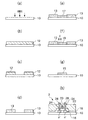
図1に、本発明の実施形態に係るシリコン膜の形成方法を用いたトランジスタの製造工程の一例を示す。 FIG. 1 shows an example of a transistor manufacturing process using a silicon film forming method according to an embodiment of the present invention.
ガラス基板10の表面上にHMDS(Hexamethyl disilazane)処理を行ない(図1(a)参照)、そのガラス基板10にフォトレジスト12を2000rpmでスピンコート成膜した(図1(b)参照)。
The surface of the
次いで、50℃で10分間、熱処理を行いフォトレジスト12の溶媒を除去した後に、フォトマスクを用いてパターン露光及び現像を行い、フォトレジスト12のパターニングを行った(図1(c)参照)。
Next, after performing heat treatment at 50 ° C. for 10 minutes to remove the solvent of the
シクロヘキサシランをトルエンに溶解させた溶液を調製し、この溶液に対して50mW/cm2の高圧水銀灯のUV光を10分照射し、その液体1mlをデカン10mlに溶解させた溶液(溶液A)を液体シリコン材料として調製した。この溶液Aを、パターニングによって形成された凹部に、インクジェット法によって塗布し、溶液Aの塗膜14を形成した(図1(d)参照)。なお、この溶液Aの塗布は、インクジェット法だけでなく、スピンコート法、ディップコート法、ミストデポジション法のいずれにおいても行うことが可能であった。
A solution in which cyclohexasilane is dissolved in toluene is prepared, and this solution is irradiated with UV light from a high-pressure mercury lamp of 50 mW / cm 2 for 10 minutes, and 1 ml of the liquid is dissolved in 10 ml of decane (solution A). Was prepared as a liquid silicon material. This solution A was applied to the recesses formed by patterning by an ink jet method to form a
このガラス基板10を図示しない真空チャンバーに入れ、1Torrの減圧下において、エネルギー密度10mW/cm2、波長308nmのエキシマランプ光を照射すると同時に、130℃で2時間加熱を行った。これにより、溶液Aの塗膜14中の溶媒であるトルエン(T)を除去すると同時に、耐熱性が付与されたフォトレジスト13を形成するための硬化処理を同時に行った(図1(e)参照)。
The
引き続き、このガラス基板10を400℃で1時間加熱し、トルエンが除去された溶液Aの塗膜14を熱分解し、アモルファスシリコン膜15を形成した(図1(f)参照)。
Subsequently, the
次に、フォトレジスト13の剥離を行うことにより、微細にパターニングされたアモルファスシリコン膜15を簡易なプロセスでガラス基板10上に成膜する事ができた(図1(g)参照)。
Next, by peeling off the
こうしてパターニングされたシリコン膜(アモルファスシリコン膜15)は、従来の薄膜トランジスタ製造にそのまま適用できるものであり、一般的に用いられているレーザー照射による再結晶でポリシリコン膜16を形成し、次いで、ゲート絶縁膜18の成膜、ゲート電極20の形成、ポリシリコン膜16へのイオン打ち込み(n+)、層間絶縁膜22の形成、コンタクトホール24の形成、ソース電極26及びドレイン電極28の形成を順次行い、ポリシリコン薄膜トランジスタ1を作製した。
The patterned silicon film (amorphous silicon film 15) can be directly applied to the manufacture of a conventional thin film transistor. A
こうして作製したトランジスタ1の特性を評価したところ、移動度は80cm2/Vsであった。従って、本発明を適用することにより、従来法より簡便かつ安価なプロセスで、性能の劣る事のないトランジスタ1を作製できることが判明した。 When the characteristics of the transistor 1 thus manufactured were evaluated, the mobility was 80 cm 2 / Vs. Therefore, it has been found that by applying the present invention, the transistor 1 having no inferior performance can be manufactured by a simpler and cheaper process than the conventional method.
このように、フォトレジストの硬化処理と液体シリコン材料(溶液A)の溶媒除去を略同時に行うことにより、工程の簡略化を図ることができる。 As described above, the process can be simplified by performing the curing process of the photoresist and the solvent removal of the liquid silicon material (solution A) substantially at the same time.
図2に、本発明の他の実施形態に係るシリコン膜の形成方法を用いたトランジスタの製造工程の一例を示す。 FIG. 2 shows an example of a manufacturing process of a transistor using a silicon film forming method according to another embodiment of the present invention.
図2(a)〜(c)に示すように、HMDS処理を行ったガラス基板10にフォトレジストを塗布し、露光、現像によりフォトレジスト12のパターニングを行うまでは実施例1と同様であるため、ここでは説明を省略する。
As shown in FIGS. 2A to 2C, the process is the same as in Example 1 until the photoresist is applied to the
次に、ガラス基板10を図示しない真空チャンバーに入れ、1Torrの減圧下において、エネルギー密度10mW/cm2、波長308nmのエキシマランプ光を照射すると同時に130℃で2時間加熱を行うことにより、耐熱性が付与されたフォトレジスト13を得た(図2(d)参照)。
Next, the
次に、ヘキサシラン1mlをキシレン10mlに溶解させた溶液(溶液B)を液体シリコン材料として調製し、フォトレジスト13のパターニングによって形成された凹部に、溶液Bをインクジェット法によって塗布し、溶液Bの塗膜17を形成した(図2(e)参照)。
Next, a solution (solution B) in which 1 ml of hexasilane is dissolved in 10 ml of xylene is prepared as a liquid silicon material, and the solution B is applied to the recesses formed by patterning the
次に、この基板10を400℃で1時間加熱し、キシレン(X)を除去するとともに、溶液Bの塗膜17を熱分解し、アモルファスシリコン膜19を形成した(図2(f)参照)。
Next, the
引き続き、実施例1と同様の要領で種々の膜を形成し、薄膜トランジスタ2を作製した(図2(h)参照)。この薄膜トランジスタ2の特性を評価したところ、移動度は90cm2/Vsであった。 Subsequently, various films were formed in the same manner as in Example 1 to manufacture the thin film transistor 2 (see FIG. 2H). When the characteristics of the thin film transistor 2 were evaluated, the mobility was 90 cm 2 / Vs.
このように、フォトレジストが液体シリコン材料(溶液B)の溶媒(この場合はキシレン)に溶解しやすい場合は、本実施例のようにフォトレジストの硬化処理を先に行うことでフォトレジストの溶解を防ぐことができる。 As described above, when the photoresist is easily dissolved in the solvent (in this case, xylene) of the liquid silicon material (solution B), the photoresist is dissolved by first performing the curing process of the photoresist as in this embodiment. Can be prevented.
1:ポリシリコン薄膜トランジスタ、10:ガラス基板、12:フォトレジスト、13耐熱性が付与されたフォトレジスト、14:溶液Aの塗膜、15、19:アモルファスシリコン膜、16:ポリシリコン膜、17:溶液Bの塗膜、18:ゲート絶縁膜、20:ゲート電極、22:層間絶縁膜、24:コンタクトホール、26:ソース電極、28:ドレイン電極 1: Polysilicon thin film transistor, 10: Glass substrate, 12: Photoresist, 13 Photoresist with heat resistance, 14: Coating film of solution A, 15, 19: Amorphous silicon film, 16: Polysilicon film, 17: Coating film of solution B, 18: gate insulating film, 20: gate electrode, 22: interlayer insulating film, 24: contact hole, 26: source electrode, 28: drain electrode
Claims (11)
前記凹部に液体シリコン材料を塗布する工程と、
前記レジストパターン及び塗布された前記液体シリコン材料に対して、光処理及び第1熱処理を行う工程と、
前記液体シリコン材料に対して、第2熱処理を行う工程と、
を含む、シリコン膜の形成方法。 Forming a resist pattern on the substrate and forming a recess;
Applying a liquid silicon material to the recess;
Performing a light treatment and a first heat treatment on the resist pattern and the applied liquid silicon material;
Performing a second heat treatment on the liquid silicon material;
A method for forming a silicon film.
前記レジストパターンに対して、光処理及び第1熱処理を行う工程と、
前記凹部に液体シリコン材料を塗布する工程と、
前記液体シリコン材料に対して、第2熱処理を行う工程と、
を含むシリコン膜の形成方法。 Forming a resist pattern on the substrate and forming a recess;
Performing a light treatment and a first heat treatment on the resist pattern;
Applying a liquid silicon material to the recess;
Performing a second heat treatment on the liquid silicon material;
A method of forming a silicon film including:
An electro-optical device manufacturing method using the device manufacturing method according to claim 10.
Priority Applications (1)
| Application Number | Priority Date | Filing Date | Title |
|---|---|---|---|
| JP2004060466A JP2005251982A (en) | 2004-03-04 | 2004-03-04 | Silicon film forming method, manufacturing method of device using the same, and manufacturing method using manufacturing method of the same device |
Applications Claiming Priority (1)
| Application Number | Priority Date | Filing Date | Title |
|---|---|---|---|
| JP2004060466A JP2005251982A (en) | 2004-03-04 | 2004-03-04 | Silicon film forming method, manufacturing method of device using the same, and manufacturing method using manufacturing method of the same device |
Publications (1)
| Publication Number | Publication Date |
|---|---|
| JP2005251982A true JP2005251982A (en) | 2005-09-15 |
Family
ID=35032179
Family Applications (1)
| Application Number | Title | Priority Date | Filing Date |
|---|---|---|---|
| JP2004060466A Pending JP2005251982A (en) | 2004-03-04 | 2004-03-04 | Silicon film forming method, manufacturing method of device using the same, and manufacturing method using manufacturing method of the same device |
Country Status (1)
| Country | Link |
|---|---|
| JP (1) | JP2005251982A (en) |
Cited By (5)
| Publication number | Priority date | Publication date | Assignee | Title |
|---|---|---|---|---|
| JP2008103686A (en) * | 2006-08-15 | 2008-05-01 | Kovio Inc | Printed dopant layer |
| US8304780B2 (en) | 2006-08-15 | 2012-11-06 | Kovio, Inc. | Printed dopant layers |
| KR101272175B1 (en) * | 2006-06-20 | 2013-06-07 | 엘지디스플레이 주식회사 | A method of fabricating polycrystalline silicon layer |
| US9196641B2 (en) | 2006-08-15 | 2015-11-24 | Thin Film Electronics Asa | Printed dopant layers |
| JP7489868B2 (en) | 2020-08-26 | 2024-05-24 | 東京エレクトロン株式会社 | Method for forming silicon film |
-
2004
- 2004-03-04 JP JP2004060466A patent/JP2005251982A/en active Pending
Cited By (5)
| Publication number | Priority date | Publication date | Assignee | Title |
|---|---|---|---|---|
| KR101272175B1 (en) * | 2006-06-20 | 2013-06-07 | 엘지디스플레이 주식회사 | A method of fabricating polycrystalline silicon layer |
| JP2008103686A (en) * | 2006-08-15 | 2008-05-01 | Kovio Inc | Printed dopant layer |
| US8304780B2 (en) | 2006-08-15 | 2012-11-06 | Kovio, Inc. | Printed dopant layers |
| US9196641B2 (en) | 2006-08-15 | 2015-11-24 | Thin Film Electronics Asa | Printed dopant layers |
| JP7489868B2 (en) | 2020-08-26 | 2024-05-24 | 東京エレクトロン株式会社 | Method for forming silicon film |
Similar Documents
| Publication | Publication Date | Title |
|---|---|---|
| KR100553857B1 (en) | Higher silan composition and mehtod of forming silicon film using thereof | |
| JP3864413B2 (en) | Method for manufacturing transistor | |
| JP3872294B2 (en) | Silicon film forming method and ink-jet ink composition | |
| JP4042685B2 (en) | Method for manufacturing transistor | |
| JP4042327B2 (en) | Thin film transistor manufacturing method | |
| JP4075308B2 (en) | Thin film transistor manufacturing method | |
| KR100436319B1 (en) | Method for forming silicon film | |
| WO2000059044A1 (en) | Method of manufacturing solar cell | |
| WO2004110929A1 (en) | Silane polymer and method for forming silicon film | |
| EP1092755A1 (en) | Coating composition | |
| KR20110046439A (en) | Aluminum ink and its manufacturing method, aluminum ink deposition method and film formed by printing and / or deposition of aluminum ink | |
| JP2005223268A (en) | Process for fabricating thin film transistor, process for fabricating display, and display | |
| JP3865106B2 (en) | Method for forming silicon film pattern | |
| JP2005089239A (en) | Method for manufacturing silicon curved surface body, silicon curved surface body, device, and method for manufacturing the device | |
| JP2005251982A (en) | Silicon film forming method, manufacturing method of device using the same, and manufacturing method using manufacturing method of the same device | |
| JP2005235852A (en) | Process for forming multilayer film and process for fabricating device | |
| JP2003318119A (en) | Silicon film and method for forming the same, liquid crystal display device, organic el display device, electronic apparatus and apparatus | |
| JP2005228793A (en) | Method for forming gate electrode made of doped silicon film, and method for manufacturing device | |
| JP2005223138A (en) | Process for depositing silicon film and process for fabricating device using silicon film deposition process | |
| WO2005038891A1 (en) | Composition for forming silicon-cobalt film, silicon-cobalt film and method for forming same | |
| JP2007165524A (en) | Semiconductor device, manufacturing method thereof, electronic equipment, and manufacturing method thereof | |
| JP2005093611A (en) | Method of manufacturing thin film transistor and device, and thin film transistor and device |