JP2005197890A - Contactless ic responder - Google Patents
Contactless ic responder Download PDFInfo
- Publication number
- JP2005197890A JP2005197890A JP2004000620A JP2004000620A JP2005197890A JP 2005197890 A JP2005197890 A JP 2005197890A JP 2004000620 A JP2004000620 A JP 2004000620A JP 2004000620 A JP2004000620 A JP 2004000620A JP 2005197890 A JP2005197890 A JP 2005197890A
- Authority
- JP
- Japan
- Prior art keywords
- circuit
- substrate
- voltage
- potential
- contact
- Prior art date
- Legal status (The legal status is an assumption and is not a legal conclusion. Google has not performed a legal analysis and makes no representation as to the accuracy of the status listed.)
- Pending
Links
- 239000000758 substrate Substances 0.000 claims description 117
- 238000001514 detection method Methods 0.000 claims description 26
- 238000004891 communication Methods 0.000 claims description 10
- 230000008859 change Effects 0.000 claims description 6
- 239000004065 semiconductor Substances 0.000 claims description 6
- 230000002123 temporal effect Effects 0.000 claims description 2
- 239000003990 capacitor Substances 0.000 abstract description 30
- 238000010586 diagram Methods 0.000 description 17
- XUIMIQQOPSSXEZ-UHFFFAOYSA-N Silicon Chemical compound [Si] XUIMIQQOPSSXEZ-UHFFFAOYSA-N 0.000 description 8
- 230000005540 biological transmission Effects 0.000 description 8
- 238000000034 method Methods 0.000 description 8
- 229910052710 silicon Inorganic materials 0.000 description 8
- 239000010703 silicon Substances 0.000 description 8
- 230000007423 decrease Effects 0.000 description 7
- 230000005674 electromagnetic induction Effects 0.000 description 5
- 238000009499 grossing Methods 0.000 description 4
- 229910044991 metal oxide Inorganic materials 0.000 description 4
- 150000004706 metal oxides Chemical class 0.000 description 4
- 230000008878 coupling Effects 0.000 description 3
- 238000010168 coupling process Methods 0.000 description 3
- 238000005859 coupling reaction Methods 0.000 description 3
- 230000003247 decreasing effect Effects 0.000 description 3
- 230000007274 generation of a signal involved in cell-cell signaling Effects 0.000 description 3
- 230000004913 activation Effects 0.000 description 2
- 230000004048 modification Effects 0.000 description 2
- 238000012986 modification Methods 0.000 description 2
- 230000008569 process Effects 0.000 description 2
- 230000002250 progressing effect Effects 0.000 description 2
- 230000009467 reduction Effects 0.000 description 2
- 230000002441 reversible effect Effects 0.000 description 2
- 230000000694 effects Effects 0.000 description 1
- 238000005516 engineering process Methods 0.000 description 1
- 239000000284 extract Substances 0.000 description 1
- 230000006870 function Effects 0.000 description 1
- 239000010410 layer Substances 0.000 description 1
- 230000004044 response Effects 0.000 description 1
- 230000000630 rising effect Effects 0.000 description 1
- 229920006395 saturated elastomer Polymers 0.000 description 1
- 239000002356 single layer Substances 0.000 description 1
Images


Abstract
Description
本発明は、リーダ・ライター等の質問器との間で、電磁波を介して非接触にデータ通信を行う非接触型ICカードやICタグ等と称される非接触型IC応答器に関し、特に、共振周波数の調整に関する技術に属する。 The present invention relates to a non-contact type IC responder referred to as a non-contact type IC card or IC tag that performs non-contact data communication with an interrogator such as a reader / writer via electromagnetic waves, It belongs to the technology related to adjustment of resonance frequency.
近年、非接触でデータの送受信を行う非接触型ICカードやICタグ等の非接触型IC応答器の利用が急速に進みつつあり、通信方式等の標準化も急速に進んでいる(例えば通信距離が10cm程度の近接型に関してISO14443、通信距離が70cm程度の近傍型に関してISO15693など)。 In recent years, the use of non-contact type IC responders such as non-contact type IC cards and IC tags that transmit and receive data without contact is rapidly progressing, and standardization of communication methods and the like is also progressing rapidly (for example, communication distance). Is ISO 14443 for the proximity type having a communication distance of about 10 cm, and ISO 15693 for the proximity type having a communication distance of about 70 cm.
この種のICカード等は、例えば、バーコードに代えて物品に付加することにより、ICカード等に記録された物品に関する情報などをリーダ・ライターによって非接触に読み込むことができるため、利便性の高い物品管理システムへの適用などが注目されている。 This type of IC card, for example, can be read in a non-contact manner by using a reader / writer to read information about the article recorded on the IC card or the like by adding it to the article instead of a barcode. Its application to high article management systems is attracting attention.
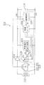
上記のような非接触型ICカードを用いたカードシステムは、例えば図20に示すような構成を有している。同図において、リーダ・ライター901は、送信部902と、受信部903と、コイル904と、共振用容量905とを備えて構成されている。また、ICカード911は、コイル912と共振用容量913とを有する共振回路と、整流用ダイオード914と、LSI負荷抵抗915として同図に示すICカード911の本体部とを備えて構成されている。
The card system using the non-contact type IC card as described above has a configuration as shown in FIG. 20, for example. In the figure, a reader /
上記のように構成されたICカードシステムでは、リーダ・ライター901とICカード911との間で、電磁波を用いた電磁誘導方式により、電力および信号の送受信が行われる。より詳しくは、リーダ・ライター901から所定の周波数の搬送波にデータ信号の重畳された電磁波が送信されると、ICカード911では、共振回路を構成するコイル912の両端に電磁誘導による電圧が誘起される。この電圧が整流されて電源電圧として用いられるとともに、データ信号が抽出されて種々の処理が行われる。
In the IC card system configured as described above, electric power and signals are transmitted and received between the reader /
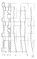
上記コイル912の両端に誘起される電圧は、図21に示すように、受信される電磁波の周波数に応じて変化し、搬送波周波数が共振回路の共振周波数f0に等しいときに最も高くなる。上記共振周波数f0は、次のように表される。
As shown in FIG. 21, the voltage induced across the
f0=1/{2×π×√(L×C)}
ここで、
L:コイル912のインダクタンス
C:共振用容量913のキャパシタンス
である。
f0 = 1 / {2 × π × √ (L × C)}
here,
L: inductance of the coil 912 C: capacitance of the
そこで、上記共振周波数f0が搬送波周波数に等しくなるように、ICカード911の製造時にコイル912のインダクタンスおよび共振用容量913のキャパシタンスが設定される。
Therefore, the inductance of the
上記のようなICカードシステムでは、バーコードを用いる場合と異なり、複数枚のICカード911からデータをまとめて読み出すことも考えられる。しかしながら、実際には、複数枚のICカードを重ねて配置した場合などには、共振周波数のずれが生じるため、上記従来のICカードシステムでは、確実なデータの読み出しを行うことができない。
In the IC card system as described above, unlike the case of using a barcode, it is conceivable to read data from a plurality of
すなわち、複数枚のICカードのコイル912が近接していると、図22に示すような結合関係による相互インダクタンスMによって、共振周波数が低下することになる。具体的には、共振周波数f1は、次のようになる。
That is, when the
f1=1/〔2×π×√{(L+M)×C}〕
ここで、
L:コイル912のインダクタンス
C:共振用容量913のキャパシタンス
M:相互インダクタンス
である。
f1 = 1 / [2 × π × √ {(L + M) × C}]
here,
L: Inductance of coil 912 C: Capacitance of resonance capacitor 913 M: Mutual inductance.
それゆえ、コイル912に誘起される電圧は前記図21に破線で示すようになり、カードが1枚のときの共振周波数f0に等しい搬送波周波数の電磁波が受信されたときの電圧は低下することになる。このような誘起電圧の低下は、近接するICカードの枚数が多いほど、また、複数のICカードが互いに近接するほど顕著になる。そして、ICカード911が動作可能な最低電圧Voを下回ると、リーダ・ライター901との通信ができなくなる。
Therefore, the voltage induced in the
なお、一般に共振周波数を搬送波周波数に同調させる技術としては、複数の容量素子を設けて選択的に切り替えるものが知られている(例えば、特許文献1、2参照)。
しかしながら、従来のICカードシステムでは、上記のように、複数枚のICカードが重ねて用いられた場合には、確実なデータの読み出しを行うことができない。 However, in the conventional IC card system, as described above, when a plurality of IC cards are used in an overlapping manner, reliable data reading cannot be performed.
また、特許文献1、2に示されているように複数の容量素子を設けると、容量素子の占める面積が大きくなり、回路規模の大幅な増大を招くことになる。
In addition, as shown in
上記の問題に鑑み、本発明は、回路規模の大幅な増大を招くことなく、複数のIC応答器が近接している場合でも共振周波数を適切に設定することができ、搬送波周波数に確実に同調させ得るようにすることを課題とする。 In view of the above problems, the present invention can appropriately set the resonance frequency even when a plurality of IC responders are close to each other without causing a significant increase in circuit scale, and reliably tunes to the carrier frequency. It is a problem to be able to make it.
上記の点に鑑み、請求項1の発明は、
質問器との間で、電磁波を介してデータ通信を行う非接触型IC応答器であって、
ゲートと、互いに接続されたソースおよびドレインとの間で容量素子を構成するとともに基板電位を可変なMOSトランジスタを有する共振回路と、
上記MOSトランジスタの上記基板電位を制御する制御回路と、
を備えたことを特徴とする。
In view of the above points, the invention of
A non-contact IC responder that performs data communication with an interrogator via electromagnetic waves,
A resonant circuit having a MOS element that forms a capacitive element between the gate and the source and drain connected to each other and has a variable substrate potential;
A control circuit for controlling the substrate potential of the MOS transistor;
It is provided with.
また、請求項2の発明は、
請求項1の非接触型IC応答器であって、
上記共振回路が、さらに、上記MOSトランジスタと直列に接続され、与えられる電位に応じて抵抗値が制御される可変抵抗を有するとともに、
上記制御回路が、さらに上記可変抵抗の抵抗値を制御するように構成されていることを特徴とする。
The invention of
The non-contact IC responder according to
The resonance circuit further includes a variable resistor connected in series with the MOS transistor and having a resistance value controlled according to a given potential.
The control circuit is further configured to control a resistance value of the variable resistor.
これらにより、MOSトランジスタの上記基板電位が制御されることによって、ゲートと、互いに接続されたソースおよびドレインとの間の容量が変化し、共振周波数が制御されるので、搬送波周波数に同調させることができる。さらに、MOSトランジスタと直列に接続された可変抵抗の抵抗値が制御されることにより、より柔軟に共振周波数を制御して同調させることができる。 As a result, the substrate potential of the MOS transistor is controlled, whereby the capacitance between the gate and the source and drain connected to each other changes, and the resonance frequency is controlled. it can. Furthermore, by controlling the resistance value of the variable resistor connected in series with the MOS transistor, the resonance frequency can be controlled and tuned more flexibly.
また、請求項3の発明は、
請求項1および請求項2のうちの何れか1項の非接触型IC応答器であって、
上記制御回路が、
上記MOSトランジスタの基板電位、および上記可変抵抗の抵抗値のうちの少なくとも何れか一方を制御する制御信号を出力する不揮発性メモリと、
上記制御信号に応じて、所定の複数種類の電位のうちの何れかを選択して、上記MOSトランジスタの基板または上記可変抵抗に与える電位設定回路と、
を備えたことを特徴とする。
The invention of
A non-contact type IC responder according to any one of
The control circuit is
A non-volatile memory that outputs a control signal for controlling at least one of the substrate potential of the MOS transistor and the resistance value of the variable resistor;
In accordance with the control signal, a potential setting circuit that selects any one of a plurality of predetermined potentials and applies the selected potential to the substrate of the MOS transistor or the variable resistor;
It is provided with.
これにより、所定のデータを不揮発メモリに記憶させることによって、共振回路が発生する電圧に対して基板に与える電位を容易に設定することができ、したがって、共振周波数を容易に設定することができる。 Thus, by storing predetermined data in the nonvolatile memory, the potential applied to the substrate can be easily set with respect to the voltage generated by the resonance circuit, and therefore, the resonance frequency can be easily set.
また、請求項4の発明は、
請求項1および請求項2のうちの何れか1項の非接触型IC応答器であって、
上記制御回路が、
上記共振回路によって受信された信号を復調して復調信号を出力する復調回路と、
上記復調信号に応じて、所定の複数種類の電位のうちの何れかを選択して、上記MOSトランジスタの上記基板および上記可変抵抗のうちの少なくとも何れか一方に与える電位設定回路と、
を備えたことを特徴とする。
The invention of claim 4
A non-contact type IC responder according to any one of
The control circuit is
A demodulation circuit that demodulates the signal received by the resonance circuit and outputs a demodulated signal;
A potential setting circuit that selects any one of a plurality of predetermined potentials according to the demodulated signal, and applies the selected potential to at least one of the substrate of the MOS transistor and the variable resistor;
It is provided with.
これにより、復調された信号に応じて基板電位等、したがって共振周波数が設定されるので、受信時に、非接触型IC応答器の外部から共振周波数を設定することがで容易にきる。 As a result, the substrate potential or the like, and thus the resonance frequency, is set according to the demodulated signal, and therefore it is easy to set the resonance frequency from the outside of the non-contact type IC responder at the time of reception.
また、請求項5の発明は、
請求項3および請求項4のうちの何れか1項の非接触型IC応答器であって、
上記所定の複数種類の電位は、それぞれ、1つの非接触型IC応答器に対応した電位、および所定の近接状態で近接した非接触型IC応答器の1種類以上の数に対応した1つ以上の電位のうちの2つ以上の電位であることを特徴とする。
The invention of claim 5
A non-contact IC responder according to any one of
The predetermined plural types of potentials are each one or more corresponding to the potential corresponding to one non-contact type IC responder and the number of one or more types of non-contact type IC responders that are close to each other in a predetermined proximity state. The potential is two or more of the potentials.
これにより、単体の非接触型IC応答器や、互いに近接した複数の非接触型IC応答器に対して共振周波数を適切に設定することが容易にできる。 Thereby, it is possible to easily set the resonance frequency appropriately for a single non-contact IC responder or a plurality of non-contact IC responders close to each other.
また、請求項6の発明は、
請求項1および請求項2のうちの何れか1項の非接触型IC応答器であって、
上記制御回路が、
上記共振回路が発生する電圧に応じて、上記MOSトランジスタの基板電位および上記可変抵抗のうちの少なくとも何れか一方を制御するように構成されていることを特徴とする。
The invention of claim 6
A non-contact type IC responder according to any one of
The control circuit is
In accordance with a voltage generated by the resonance circuit, at least one of the substrate potential of the MOS transistor and the variable resistance is controlled.
これにより、共振回路が発生する電圧に応じて基板電位等が制御されるので、共振周波数を自動的に調整することができる。 Thereby, since the substrate potential and the like are controlled according to the voltage generated by the resonance circuit, the resonance frequency can be automatically adjusted.
また、請求項7の発明は、
請求項6の非接触型IC応答器であって、
上記制御回路が、上記MOSトランジスタの上記基板および上記可変抵抗のうちの少なくとも何れか一方に所定の電位が与えられた状態で上記共振回路が発生する電圧に応じて、上記MOSトランジスタの上記基板または上記可変抵抗に与える電位を切り替えるように構成されていることを特徴とする。
The invention of claim 7
The non-contact IC responder according to claim 6, wherein
In accordance with a voltage generated by the resonance circuit in a state where a predetermined potential is applied to at least one of the substrate of the MOS transistor and the variable resistor, the control circuit is configured such that the substrate of the MOS transistor or It is configured to switch the potential applied to the variable resistor.
また、請求項8の発明は、
請求項7の非接触型IC応答器であって、
上記制御回路が、上記共振回路が発生する電圧が所定の電圧以下である場合に、上記MOSトランジスタの上記基板または上記可変抵抗に与える電位を順次切り替えるように構成されていることを特徴とする。
The invention of claim 8
The non-contact IC responder according to claim 7, wherein
The control circuit is configured to sequentially switch a potential applied to the substrate or the variable resistor of the MOS transistor when a voltage generated by the resonance circuit is equal to or lower than a predetermined voltage.
これにより、共振回路が発生する電圧が所定の電圧以下であるかどうかなどの簡単な検出をするだけで、基板電位等を制御して、共振周波数を自動的に調整することができる。 As a result, it is possible to automatically adjust the resonance frequency by controlling the substrate potential or the like only by simply detecting whether or not the voltage generated by the resonance circuit is equal to or lower than a predetermined voltage.
また、請求項9の発明は、
請求項6の非接触型IC応答器であって、
上記制御回路が、所定の時間経過の前後における上記共振回路が発生する電圧の変化に応じて、上記基板および上記可変抵抗のうちの少なくとも何れか一方に与える電位を制御するように構成されていることを特徴とする。
The invention of claim 9
The non-contact IC responder according to claim 6, wherein
The control circuit is configured to control a potential applied to at least one of the substrate and the variable resistor in accordance with a change in voltage generated by the resonance circuit before and after a predetermined time elapses. It is characterized by that.
また、請求項10の発明は、
請求項9の非接触型IC応答器であって、
上記制御回路が、
上記共振回路が発生する電圧の時間的変化を検出する検出回路と、
上記共振回路が発生する電圧を昇圧して上記基板に与えるチャージポンプ回路とを備え、
上記共振回路が発生する電圧が上昇している場合に、上記チャージポンプ回路を動作させるように構成されていることを特徴とする。
The invention of claim 10 provides
The contactless IC transponder of claim 9, wherein
The control circuit is
A detection circuit for detecting a temporal change in voltage generated by the resonance circuit;
A charge pump circuit that boosts the voltage generated by the resonant circuit and applies the boosted voltage to the substrate;
The charge pump circuit is configured to operate when the voltage generated by the resonance circuit is rising.
これらにより、共振回路が発生する電圧の増減に応じて基板電位等が設定されることにより、上記共振回路の発生する電圧が極大になるように基板電位等が制御される。すなわち、共振周波数を自動的かつ適切に調整することが容易にできる。 Accordingly, the substrate potential and the like are controlled so that the voltage generated by the resonance circuit is maximized by setting the substrate potential and the like in accordance with the increase and decrease of the voltage generated by the resonance circuit. That is, the resonance frequency can be easily adjusted automatically and appropriately.
また、請求項11の発明は、
請求項1の非接触型IC応答器であって、
上記MOSトランジスタは、少なくともp型半導体ウェハ上に形成されたn型ウェル上にさらに形成されたPMOSトランジスタ、または少なくともn型半導体ウェハ上に形成されたp型ウェル上にさらに形成されたNMOSトランジスタであることを特徴とする。
The invention of claim 11
The non-contact IC responder according to
The MOS transistor is a PMOS transistor further formed on an n-type well formed on at least a p-type semiconductor wafer, or an NMOS transistor further formed on a p-type well formed on at least an n-type semiconductor wafer. It is characterized by being.
これにより、p型半導体ウェハとn型ウェルとの間、またはn型半導体ウェハとp型ウェルとの間で、pn接合の逆方向電圧になるように、基板(ウェル)に電位を与えることにより、同一基板上の他のNMOS、PMOSトランジスタの動作に影響を与えないようにすることが容易にできる。なお、n型ウェルやp型ウェルは1層に限らず、多層に形成されていたり、ツインウェルとして形成されていたりしてもよい。 Thereby, by applying a potential to the substrate (well) so as to be a reverse voltage of the pn junction between the p-type semiconductor wafer and the n-type well or between the n-type semiconductor wafer and the p-type well. The operation of other NMOS and PMOS transistors on the same substrate can be easily prevented from being affected. Note that the n-type well and the p-type well are not limited to one layer, and may be formed in multiple layers or as a twin well.
本発明によると、MOSトランジスタの基板電位が制御されることによって共振周波数が設定されるので、回路規模の大幅な増大を招くことなく、複数のIC応答器が近接している場合でも共振周波数を適切に設定することが容易にでき、搬送波周波数に確実に同調させ得るようにすることができる。 According to the present invention, since the resonance frequency is set by controlling the substrate potential of the MOS transistor, the resonance frequency can be set even when a plurality of IC responders are close without causing a significant increase in circuit scale. It can be easily set appropriately and can be reliably tuned to the carrier frequency.
以下、本発明の実施形態を図面に基づいて詳細に説明する。 Hereinafter, embodiments of the present invention will be described in detail with reference to the drawings.
《発明の実施形態1》
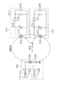
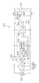
図1は本発明の実施形態1に係る非接触型IC応答器であるICカードを用いたカードシステムの概略構成を示す回路図である。同図において、リーダ・ライター101は、送信部102と、受信部103と、コイル104(ループアンテナ)と、共振用容量105とを備えて構成されている。また、ICカード111は、コイル112および所定の容量に可変に制御される容量制御共振用容量113を有する共振回路と、整流用ダイオード114と、平滑容量115と、LSI負荷抵抗116として同図に示すICカード111の本体部とを備えて構成されている。上記容量制御共振用容量113は、具体的には、図2に示すように、基板電位を可変に設定し得るPMOSトランジスタ121と、上記基板電位を制御する基板電位制御回路122とを備えて構成されている。ここで、上記基板電位制御回路122は、ICカード111の本体部が動作し得る電源電圧よりも低い電源電圧、すなわち後述するように例えばICカード111が重ねて用いられたために共振周波数がずれている場合に得られる電源電圧でも動作し得るように構成されている。具体的には、例えば基板電位制御回路122を構成するトランジスタの閾値が本体部よりも低く設定されている。
FIG. 1 is a circuit diagram showing a schematic configuration of a card system using an IC card which is a non-contact type IC responder according to
(PMOSトランジスタ121の構造および特性)
PMOSトランジスタ121は、例えば図3に示すように、p型シリコンウェハ131上に形成されたn型ウェル132上に、ソースまたはドレインとなるp型領域133と、金属酸化膜134を介して配置されたゲート電極135と、n型ウェル132の電位を制御するための基板電位制御端子Bが接続されたn型領域136とが形成されて構成されている。
(Structure and characteristics of PMOS transistor 121)
For example, as shown in FIG. 3, the
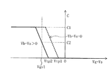
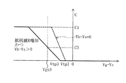
上記ゲートと、互いに接続されたソースおよびドレインとの間には容量が生じるとともに、n型領域136を介してn型ウェル132の電位を変化させることにより、上記容量が可変に制御されるようになっている。より詳しくは、図4に示すように、ゲート電圧(Vg−Vs)(横軸)および基板電圧(Vb−Vs)に応じて、ソース−ゲート間の容量C(縦軸)が変化する特性を有している。すなわち、例えば基板電圧(Vb−Vs)=0である場合には(図4の破線)、ゲート電圧(Vg−Vs)が所定の閾値Vtp1よりも低くなると、ゲート直下にチャネルが形成され、容量Cは、ゲート電圧(Vg−Vs)が低くなるのに伴って大きくなり、やがてC1になって飽和する。また、基板電圧(Vb−Vs)>0の場合には(図4の実線)、上記閾値Vtp1はVtp2にシフトし、同様に、ゲート電圧(Vg−Vs)が上記閾値Vtp2よりも低くなるのに伴って、容量Cが大きくなる。そこで、例えばゲート電圧(Vg−Vs)が同図に示すVgs1だとすると、基板電圧(Vb−Vs)=0の状態から基板電圧(Vb−Vs)>0の状態に変化させることにより、ソース−ゲート間の容量CをC1からC2に低下させることができる。なお、正確には、ゲート電圧(Vg−Vs)は、コイル112の両端に生じる搬送波周波数で正負に変化する電圧になるが、平均的に、所定のゲート電圧(Vg−Vs)のときの容量として上記のように制御することができる。
A capacitance is generated between the gate and the source and drain connected to each other, and the potential is controlled variably by changing the potential of the n-type well 132 through the n-
ここで、n型ウェル132はソース−ゲート間の容量を制御するためには必ずしも設けなくてもよいが、同図に示すようにn型ウェル132上にPMOSトランジスタ121が形成されていることにより、基板電圧(Vb−Vs)>0になる場合、すなわち、例えば前記図3のp型シリコンウェハ131がGND(接地)電位に固定されていて、n型領域136に正の電圧が印加される場合に、n型ウェル132とp型シリコンウェハ131との間には逆方向電圧が印加されることになるので、p型シリコンウェハ131上に形成された他のNMOSトランジスタ141等に影響を与えることなく(閾値を変化させたりすることなく)安定した動作をさせることができる。
Here, the n-
(基板電位制御回路122の詳細な構成)
基板電位制御回路122は、例えば図5に示すように、不揮発性メモリ123と、基板電位発生回路124と、セレクタ125とを備えて構成されている。
(Detailed Configuration of Substrate Potential Control Circuit 122)
For example, as shown in FIG. 5, the substrate
上記不揮発性メモリ123は、起動信号が入力されると、所定のデータを選択信号φ1〜φ3として出力するようになっている。具体的には、そのICカード111が1枚だけで用いられるか、2枚が重ねられて用いられるか、または3枚が重ねられて用いられるかの使用形態に応じて、あらかじめ選択信号φ3、φ2、またはφ1だけがH(High)レベルになるデータが書き込まれる。上記不揮発性メモリ123としては、例えば電荷蓄積型やヒューズ切断型などのプログラマブルメモリが用いられる。
The
基板電位発生回路124は、整流用ダイオード114によって整流された電圧を例えばチャージポンプ回路等により昇圧または降圧して、複数段階の所定の制御電圧V1〜V3を発生するようになっている。上記所定の制御電圧V1〜V3は、PMOSトランジスタ121の基板に印加されたときに、ICカード111の使用枚数に応じた共振周波数が得られるように設定されている。
The substrate
セレクタ125は、上記不揮発性メモリ123から出力される選択信号φ1〜φ3に応じて、基板電位発生回路124から出力される制御電圧V1〜V3を選択的に切り替え、PMOSトランジスタ121の基板電位を設定するようになっている。上記セレクタ125と前記基板電位発生回路124とによって基板電位設定回路が構成される。なお、選択される制御電圧はV1〜V3の3段階に限らず、2段階でもよいし、より多くの段階になるようにしてもよい。
The
(ICカード111の動作)
上記のように構成されたICカードシステムでは、リーダ・ライター101とICカード111との間で、電磁波を用いた電磁誘導方式により、電力および信号の送受信が行われる。より詳しくは、リーダ・ライター101から所定の周波数の搬送波にデータ信号の重畳された電磁波が送信されると、ICカード111では、共振回路を構成するコイル112の両端に電磁誘導による電圧が誘起される。この電圧が整流されて電源電圧として用いられるとともに、データ信号が抽出されて種々の処理が行われる。
(Operation of IC card 111)
In the IC card system configured as described above, power and signals are transmitted and received between the reader /
ここで、複数枚のICカード111が重ねて配置され、各ICカード111のコイル112が互いに近接する場合などには、コイル112の結合関係による相互インダクタンスMによって共振周波数が低下し、コイル112に誘起される電圧が低下することになる。そこで、本実施形態のICカード111では、あらかじめ、ICカード111の使用形態、例えば1枚だけのICカード111が用いられるのか、または所定枚数のICカード111が重ねられて用いられるのかに応じて、不揮発性メモリ123に所定のデータが記憶されることにより、PMOSトランジスタ121のソース−ゲート間の容量が設定され、共振周波数が一定に保たれる。
Here, when a plurality of
以下、基板電位制御回路122によって上記基板電圧(Vb−Vs)が制御される際の具体的な動作について説明する。図6は、ICカード111の各部の電圧を示すタイミングチャートである。リーダ・ライター101から発せられた電磁波がICカード111で受信されると、コイル112の両端には、コイル受信波Vcoilが発生する。これが整流用ダイオード114で整流され、平滑容量115によって平滑されると、電源電圧VDDが得られる。より詳しくは、受信が開始された後、平滑容量115の蓄積電荷が定常状態に達するまでは、上記電源電圧VDDは徐々に上昇する。上記電源電圧VDDの上昇に伴って、基板電位発生回路124から出力される制御電圧V1〜V3も徐々に上昇し、やがて、それぞれあらかじめ設定された一定の電圧になる。(なお、図6においては電圧V3〜V1が順に定常状態に達するように描かれているが、電圧の昇降圧の方式によっては必ずしもこのように変化せず、例えば同図に2点差線で示すように変化するようにしてもよい。)このとき、基板電圧(Vb−Vs)は、例えばセレクタ125によってV1〜V3の何れの電圧も選択されていなかったとすると、VDD−約0.7V(p−n接合による降下電圧)になる。
Hereinafter, a specific operation when the substrate voltage (Vb−Vs) is controlled by the substrate
そして、例えば電源電圧VDDが所定のレベルに達すると、または電源電圧VDDが所定のレベルに達してから所定の時間だけ経過すると、図示しないタイマ回路からメモリ起動信号が不揮発性メモリ123に入力され、不揮発性メモリ123は、重ねて用いられるICカード111の枚数に応じて、例えば3枚の場合には、あらかじめ記憶された選択信号φ1がHレベルになるデータを出力する。これによって、電圧V1がPMOSトランジスタ121の基板に印加され、共振周波数が搬送波周波数に同調する一定の周波数に保たれる。すなわち、3枚のICカード111が重ねて用いられる場合には、1枚だけが用いられる場合に比べて相互インダクタンスMによりインダクタンス成分がが増大する一方、電圧V3よりも高い所定の電圧V1がPMOSトランジスタ121の基板に印加されることによってPMOSトランジスタ121の容量が減少し、適切に同調がとられる。
For example, when the power supply voltage VDD reaches a predetermined level, or when a predetermined time elapses after the power supply voltage VDD reaches the predetermined level, a memory activation signal is input to the
上記のように、重ねて用いられるICカード111の枚数に応じたデータがあらかじめ不揮発性メモリ123に記憶されることにより、電源投入時(受信開始時)に相互インダクタンスMの影響に応じた共振容量に設定され、搬送波周波数に確実に同調して充分な電源電圧が得られるとともにデータ信号の抽出や処理が適切に行われる。また、上記のようにMOSトランジスタの基板電圧を制御して共振周波数を制御する構成は、制御電力を非常に小さく抑えられる点で、ICカード111などのような非接触型IC応答器に適している。
As described above, the data corresponding to the number of
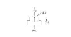
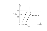
なお、上記の例では、共振用容量としてPMOSトランジスタ121が用いられる例を示したが、これに限らず、例えば図7に示すようなNMOSトランジスタ151が用いられるようにしてもよい。すなわち、例えば図8に示すように、n型シリコンウェハ161上に形成されたp型ウェル162上に、ソースまたはドレインとなるn型領域163と、金属酸化膜164を介して配置されたゲート電極165と、p型ウェル162の電位を制御するための基板電位制御端子Bが接続されたp型領域166とが形成されたNMOSトランジスタ151を用いることができる。この場合には、図9に示すように、基板電圧(Vb−Vs)<0になると、基板電圧(Vb−Vs)=0の場合に比べて、同じゲート電圧Vgs2であってもソース−ゲート間の容量CがC1からC2に低下する。それゆえ、基板電位発生回路124に電源電圧VDDを極性反転させた電圧を発生させることによって、上記の場合と同様にp型ウェル162の電位を変化させて共振周波数を制御することができるとともに、n型シリコンウェハ161上に形成された他のPMOSトランジスタ171等に影響を与えないようにして(閾値を変化させたりすることなく)安定した動作をさせることができる。また、上記n型ウェル132やp型ウェル162は、1重に形成されるのに限らず、多重に形成されるようにしてもよい。
In the above example, the
《発明の実施形態2》
図10は、本発明の実施形態2に係るICカード211における基板電位制御回路222の構成を示す回路図である。なお、以下の実施形態において、前記実施形態1等と同様の機能を有する構成要素については同一の符号を付して説明を省略する。
<<
FIG. 10 is a circuit diagram showing a configuration of the substrate
この基板電位制御回路222は、前記実施形態1(図5)の基板電位制御回路122に比べて、不揮発性メモリ123に代えて、復調回路223および制御レジスタ224を備えている点が異なっている。
The substrate
復調回路223は、リーダ・ライター101から送信されるデータ信号の抽出を行い、基板電位設定データRXが受信された場合には、その基板電位設定データRXを制御レジスタ224に出力するようになっている。
The
制御レジスタ224は、上記基板電位設定データRXを保持するとともに、選択信号φ1〜φ3としてセレクタ125に出力するようになっている。
The
このように構成されたICカード211では、図11に示すように、リーダ・ライター101から所定のプロトコルで基板電位設定データRXが搬送波に重畳されて送信されることにより、前記実施形態1と同様にPMOSトランジスタ121の基板電位をV1〜V3に設定することによって共振周波数を制御することができる。すなわち、前記実施形態1のようにICカード211に対して使用形態(重ねて用いられる枚数)に応じた設定をしなくても、リーダ・ライター101から共振周波数を制御して、適切に送受信されるようにすることができる。また、通信状態において何度でも基板電位を変更して共振周波数を変化させることもできる。さらに、ICカード211で電源電圧VDDを検出してリーダ・ライター101に送信したり、リーダ・ライター101で電磁誘導の結合度に応じて同調程度を検出したりして、共振周波数を制御し、適切な同調状態が自動的に得られるようにすることもできる。
In the
《発明の実施形態3》
図12は、本発明の実施形態3に係るICカード311における基板電位制御回路322の構成を示す回路図である。この基板電位制御回路322は、前記実施形態1(図5)の基板電位制御回路122に比べて、不揮発性メモリ123に代えて、電圧検出回路323およびラッチ回路324を備えている点が異なっている。
<<
FIG. 12 is a circuit diagram showing a configuration of the substrate
電圧検出回路323は、電源電圧VDDを検出し、そのレベルが複数段階のレベルのうちの何れであるかを示す検出信号を出力する。
The
ラッチ回路324は、受信開始時には、例えば選択信号φ3がHレベルになる信号をセレクタ125に出力し、電源電圧VDDが所定のレベルに達してから所定の時間だけ経過したときにラッチ信号が入力されると、電圧検出回路323から出力される検出信号を保持するとともに、その検出信号に応じて選択信号φ1〜φ3の何れかだけがHレベルになる信号を出力する。これによって、制御電圧V1〜V3の何れかがPMOSトランジスタ121の基板に印加され、共振周波数が搬送波周波数に同調する。
The
すなわち、例えば、受信の開始時にセレクタ125によって電圧V3が選択されて、PMOSトランジスタ121の基板に印加されるようにするとともに、その状態で、1枚のICカード311単体のコイル112とPMOSトランジスタ121の容量とによる共振周波数が搬送波周波数に一致するように設定されているとすると、一定の送信出力を有するリーダ・ライター101から一定の距離のところに1枚のICカード311が置かれている場合には、電源電圧VDDとして一定の電圧が得られる。ところが、複数枚のICカード311が互いに近接して置かれている場合には、前記のように相互インダクタンスMにより共振周波数が低下するため、電源電圧VDDは上記一定の電圧よりも低くなる。そこで、その低下した電源電圧VDDに応じて、電圧V3よりも高い所定の電圧V1、V2がPMOSトランジスタ121の基板に印加されることによって、PMOSトランジスタ121の容量が減少し、共振周波数が高くなるので、適切に同調がとられ、充分な電源電圧が得られるとともにデータ信号の抽出や処理が適切に行われる。
That is, for example, the voltage V3 is selected by the
なお、受信の開始時にPMOSトランジスタ121の基板に印加される電圧は、上記電圧V3に限らず、一定の電圧であればよく、その電圧によって定まる共振周波数と電源電圧VDDとに応じて、基板電位発生回路124が発生する電圧が設定されていればよい。
Note that the voltage applied to the substrate of the
上記のように、複数枚のICカード311が重なっている場合などでも、リーダ・ライター101とICカード311との相互配置関係(距離等)が決まっていて、かつ、リーダ・ライター101の出力が所定の一定値であるような場合には、相互インダクタンスMの影響を電源電圧VDDによって検出することができるため、電源投入時(受信開始時)に上記相互インダクタンスMの影響を打ち消すような共振容量が設定され、自動的に適切な同調状態が得られるようにすることができる。
As described above, even when a plurality of
《発明の実施形態4》
図13は、本発明の実施形態4に係るICカード411における基板電位制御回路422の構成を示す回路図である。この基板電位制御回路422は、前記実施形態1(図5)の基板電位制御回路122に比べて、不揮発性メモリ123に代えて、電圧検出回路423、AND回路424、およびシフトレジスタ425を備えている点が異なっている。
<< Embodiment 4 of the Invention >>
FIG. 13 is a circuit diagram showing a configuration of the substrate
電圧検出回路423は、電源電圧VDDが所定の基準電圧、すなわちICカード411の本体部が適切に動作する電圧よりも低い場合に、Hレベルの検出信号を出力するようになっている。(なお、電圧検出回路423を含む基板電位制御回路422自体は、実施形態1で説明したようにICカード411の本体部が適切に動作する電圧よりも低い電圧でも動作し得るように構成されている。)
AND回路424は、電圧検出回路423からHレベルの検出信号が出力されている場合に、クロック信号を出力するようになっている。
The
The AND
シフトレジスタ425は、AND回路424からクロック信号が入力されるごとに、選択信号φ1〜φ3の何れかを順次Hレベルにするようになっている。なお、受信の開始時にHレベルになる選択信号は、特に定まっていなくてもよいが、例えば最も使用される頻度が高いICカード411の枚数に対応するように設定すれば、迅速に送受信が開始される可能性を高くすることができる。
Each time the clock signal is input from the AND
上記のように構成されたICカード411では、ある時点でPMOSトランジスタ121の基板に印加される制御電圧V1〜V3が、実際に重ねて用いられるICカード411の枚数に対応していないために同調周波数がずれて、得られる電源電圧VDDが所定の基準電圧よりも低い場合には、順次他の制御電圧V1〜V3が切り替えられてPMOSトランジスタ121の基板に印加される。そして電源電圧VDDが所定の基準電圧以上になると、電圧検出回路423から出力される検出信号がL(Low)レベルになり、シフトレジスタ425はその時点の出力状態(選択信号φ1〜φ3の何れがHレベルであるか)を維持することによって、基板に印加される制御電圧V1〜V3も維持され、その制御電圧V1〜V3に応じた同調状態に保たれる。すなわち、リーダ・ライター101とICカード411との距離が一定でない場合や、リーダ・ライター101の出力が所定の一定値出ないような場合でも、少なくとも何れかの制御電圧V1〜V3によって所定の電源電圧VDDが得られれば、自動的に適切な送受信が行われる。
In the
上記のような制御では、必ずしも正確な同調が行われるとは限らない(電源電圧VDDのレベルが極大になるとは限らない)が、何れかの制御電圧V1〜V3によって本体部が動作可能な電源電圧VDDが得られさえすれば、適切に送受信させることができる。また、リーダ・ライター101とICカード411との距離が離れすぎているなどのために何れの制御電圧V1〜V3によっても所望の電源電圧VDDが得られない場合には、例えばリーダ・ライター101から警報音を発して、再度ICカード411をリーダ・ライター101に近づけるように促すことなどによって適切に送受信できればよく、さらに、送受信できない場合には単に送受信不能として処理すればよいとする利用形態も現実的に可能である。それゆえ、上記のように簡潔な構成で、自動的に同調させて送受信させることが可能となる。
In the control as described above, accurate tuning is not always performed (the level of the power supply voltage VDD is not necessarily maximized), but the power supply that can operate the main body by any of the control voltages V1 to V3. As long as the voltage VDD is obtained, transmission and reception can be performed appropriately. Further, when the desired power supply voltage VDD cannot be obtained by any of the control voltages V1 to V3 because the distance between the reader /
《発明の実施形態5》
用いられるICカードの枚数にかかわらず、共振周波数を自動的にほぼ正確に同調させることができるICカードの例を説明する。
<< Embodiment 5 of the Invention >>
An example of an IC card that can automatically tune the resonance frequency almost accurately regardless of the number of IC cards used will be described.
実施形態5のICカード511は、図14に示すように、前記実施形態1(図5)の基板電位制御回路122に代えて、電圧検出回路512と、チャージポンプ回路513と、電圧低下回路514とを備えている。
As shown in FIG. 14, the
上記電圧検出回路512は、タイミング信号発生回路512a、容量素子512b・512c、PMOSトランジスタ512d〜512f、およびオフセットコンパレータ512gを有している。PMOSトランジスタ512d〜512fは、タイミング信号発生回路512aから出力されるタイミング信号Vc1、Vc2に応じてON/OFFし、容量素子512cに所定の時点での電源電圧Vd2を保持させる一方、容量素子512bにその後所定の時間経過後の電源電圧Vd1を保持させるようになっている。オフセットコンパレータ512gは、容量素子512bに保持されている電圧Vd1が容量素子512cに保持されている電圧Vd2よりも高い場合、すなわち電源電圧VDDが時間の経過とともに上昇している場合には、検出信号Vn1をLレベルにする一方、それ以外の場合にはHレベルにするようになっている。
The
チャージポンプ回路513は、NOT回路513a、AND回路513b、NOT回路513c、容量素子513d・513e、NMOSトランジスタ513f〜513h、ダイオード513i、および容量素子513jを有し、電源電圧VDDを徐々に昇圧した電圧をPMOSトランジスタ121の基板電圧Vbとして出力するようになっている。より詳しくは、NOT回路513aは、受信された(整流される前の)信号に応じてH、Lレベルを交互に繰り返す信号を出力するようになっている。AND回路513bは、タイミング信号Vc2がHレベルで、オフセットコンパレータ512gの検出信号Vn1がLレベルの場合に、NOT回路513aの出力に応じてH、Lレベルを交互に繰り返す信号を出力し、NOT回路513cはAND回路513bの出力を反転した信号Vp1を出力するようになっている。そこで、NMOSトランジスタ513g・513hが交互にON/OFFすることにより、容量素子513eに蓄積される電荷によって昇圧された電圧がダイオード513iを介して容量素子513jに保持され、出力される。
The
また、電圧低下回路514は、NMOSトランジスタ514a、プルアップ抵抗514b、PMOSトランジスタ514c、および電流制限回路514dを有している。この電圧低下回路514は、オフセットコンパレータ512gから出力される検出信号Vn1がHレベルである場合に、NMOSトランジスタ514aおよびPMOSトランジスタ514cがONになることにより、容量素子513jに蓄積された電荷を放電し、基板電圧Vbを徐々に低下させるようになっている。
The
図15は上記のように構成されたICカード511の各部の信号を示すタイミングチャートである。同図に示すタイミングAでは、タイミング信号Vc1、Vc2がともにHレベルになり、PMOSトランジスタ512d〜512fがOFFになるので、その直前の電源電圧VDDが容量素子512b・512cに保持される。タイミングB〜Cの期間には、タイミング信号Vc1がLレベルになってPMOSトランジスタ512dだけがONになり、各時点での電源電圧Vd1が容量素子512bに印加される。そこで、上記電圧Vd1が電圧Vd2よりも高ければ、オフセットコンパレータ512gから出力される検出信号Vn1がLレベルになり、NOT回路513cから出力される信号Vp1はH、Lレベルを交互に繰り返して、基板電圧Vbは徐々に上昇する。一方、電圧Vd1が電圧Vd2以下であれば、オフセットコンパレータ512gから出力される検出信号Vn1はHレベルになり、NMOSトランジスタ514aおよびPMOSトランジスタ514cがONになり、基板電圧Vbは徐々に低下する。
FIG. 15 is a timing chart showing signals at various parts of the
上記のように、電源電圧VDDが上昇しつつある場合には、チャージポンプ回路513によって基板電圧を徐々に上昇させる一方、電源電圧VDDが変化しないか低下しつつある場合には、基板電圧を徐々に低下させることによって、用いられるICカード511の枚数にかかわらず、電源電圧VDDがほぼ極大になるように制御することができる(理論的には、容量素子512b・512cに電源電圧VDDが保持される時間差を無限に短くすれば基板電圧Vbを連続的に変化させて電源電圧VDDを正確に極大にできることになる。)。このようなICカード511は、前記実施形態4のICカード411等に比べれば回路規模は多少大きいが、必要な電源電圧VDDが得られる程度に同調させれば十分なので、通常の受信装置程の高い同調精度や応答性能は必要なく、それゆえ、比較的簡素な回路で必要十分な同調制御を行わせることが容易にできる。
As described above, when the power supply voltage VDD is increasing, the substrate voltage is gradually increased by the
なお、初期状態で十分高い電圧が基板に与えられるようにすれば、電源電圧VDDが低下しつつある場合に、チャージポンプ回路513によって基板電圧を徐々に上昇させる一方、電源電圧VDDが変化しないか上昇しつつある場合に、基板電圧を徐々に低下させるようにしてもよいが、通常は、基板に特に外部から電圧を印加しなければ、基板電圧はVDD−約0.7Vになるので、電源電圧VDDが上昇しつつある場合に、基板電圧を上昇させるように構成する方が容易である。
If a sufficiently high voltage is applied to the substrate in the initial state, when the power supply voltage VDD is decreasing, the substrate voltage is gradually increased by the
《発明の実施形態6》
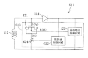
図16は、本発明の実施形態3に係るICカード611の構成を示す回路図である。このICカード611には、実施形態1のICカード111における容量制御共振用容量113に代えて、さらに、PMOSトランジスタ121と直列に接続された可変抵抗621と抵抗値制御回路622とを有する容量制御共振用容量613が設けられている。上記可変抵抗621は、具体的には、例えば制御電圧としてのゲート電圧が抵抗値制御回路622によって制御されることにより抵抗値Rが変化するp型またはn型のMOSトランジスタが用いられる。また、抵抗値制御回路622は、基板電位制御回路122、または実施形態2(図10)等の基板電位制御回路222等と同様の構成を有し、電源電圧VDD、またはリーダ・ライター101からの設定データに基づいて、所定の制御電圧を可変抵抗621に印加するようになっている。なお、可変抵抗621はPMOSトランジスタ121と並列に接続されるようにしてもよいが、上記のように直列に接続する方が消費電力を小さく抑えることができる。
Embodiment 6 of the Invention
FIG. 16 is a circuit diagram showing a configuration of an
上記のように、PMOSトランジスタ121の基板電圧(Vb−Vs)が制御されるとともに、可変抵抗621の抵抗値Rが制御される場合には、これらのPMOSトランジスタ121と可変抵抗621との合成容量は図17に示すようになる。
As described above, when the substrate voltage (Vb−Vs) of the
すなわち、例えば可変抵抗621の抵抗値Rが0で、かつ、基板電圧(Vb−Vs)=0の場合には(図17の破線)、実施形態1(図4)で説明したのと同じく、ゲート電圧(Vg−Vs)が低くなるのに伴って、容量Cが0からC1に変化する(大きくなる)。これに対して、可変抵抗621の抵抗値Rが所定の抵抗値に増加するとともに、基板電圧(Vb−Vs)>0になると(図17の実線)、閾値Vtp1がVtp3にシフトし、ゲート電圧(Vg−Vs)が上記閾値Vtp3よりも低くなるのに伴って、抵抗値Rが大きいほど緩やかな勾配で容量Cが大きくなる。そこで、例えばゲート電圧(Vg−Vs)が同図に示すVgs3だとすると、基板電圧(Vb−Vs)=0の状態から基板電圧(Vb−Vs)>0の状態に変化させるとともに抵抗値Rを大きくすることにより、ソース−ゲート間の容量CをC1からC3に低下させることができる。それゆえ、実施形態1等の場合と同様に、複数のICカード611が近接して共振周波数が低下する場合などに、基板電圧(Vb−Vs)および抵抗値Rを制御して共振用容量を小さくすることにより、共振用容量を段階的または連続的に微調整し、搬送波周波数に確実に同調させて安定した電力とデータ信号が取得されるようにすることができる。
That is, for example, when the resistance value R of the
なお、本実施形態6においても、上記PMOSトランジスタ121に代えて、図18に示すようなNMOSトランジスタ151を用い、図19に示すように容量が変化する特性を利用して、共振周波数を制御するようにしてもよい。
In the sixth embodiment, an
本発明にかかる非接触型IC応答器は、MOSトランジスタの基板電位が制御されることによって共振周波数が設定されるので、回路規模の大幅な増大を招くことなく、複数のIC応答器が近接している場合でも共振周波数を適切に設定することができ、搬送波周波数に確実に同調させ得るようにすることができる効果を有し、リーダ・ライター等の質問器との間で、電磁波を介して非接触にデータ通信を行う非接触型ICカードやICタグ等と称される非接触型IC応答器に関し、特に、共振周波数の調整に関する技術等として有用である。 In the non-contact type IC responder according to the present invention, since the resonance frequency is set by controlling the substrate potential of the MOS transistor, a plurality of IC responders are arranged close to each other without causing a significant increase in circuit scale. The resonance frequency can be set appropriately even when the signal is received, and it has the effect of being able to be surely tuned to the carrier wave frequency. The present invention relates to a non-contact type IC responder called a non-contact type IC card or IC tag that performs data communication in a non-contact manner, and is particularly useful as a technique for adjusting a resonance frequency.
101 リーダ・ライター
102 送信部
103 受信部
104 コイル
105 共振用容量
111 ICカード
112 コイル
113 容量制御共振用容量
114 整流用ダイオード
115 平滑容量
116 LSI負荷抵抗
121 PMOSトランジスタ
122 基板電位制御回路
123 不揮発性メモリ
124 基板電位発生回路
125 セレクタ
131 p型シリコンウェハ
132 n型ウェル
133 p型領域
134 金属酸化膜
135 ゲート電極
136 n型領域
141 NMOSトランジスタ
151 NMOSトランジスタ
161 n型シリコンウェハ
162 p型ウェル
163 n型領域
164 金属酸化膜
165 ゲート電極
166 p型領域
171 PMOSトランジスタ
211 ICカード
222 基板電位制御回路
223 復調回路
224 制御レジスタ
311 ICカード
322 基板電位制御回路
323 電圧検出回路
324 ラッチ回路
411 ICカード
422 基板電位制御回路
423 電圧検出回路
424 AND回路
425 シフトレジスタ
511 ICカード
512 電圧検出回路
512a タイミング信号発生回路
512b・512c 容量素子
512d〜512f PMOSトランジスタ
512g オフセットコンパレータ
513 チャージポンプ回路
513a NOT回路
513b AND回路
513c NOT回路
513d・513e 容量素子
513f〜513h NMOSトランジスタ
513i ダイオード
513j 容量素子
514 電圧低下回路
514a NMOSトランジスタ
514b プルアップ抵抗
514c PMOSトランジスタ
514d 電流制限回路
611 ICカード
613 容量制御共振用容量
621 可変抵抗
622 抵抗値制御回路
101 Reader /
Claims (11)
ゲートと、互いに接続されたソースおよびドレインとの間で容量素子を構成するとともに基板電位を可変なMOSトランジスタを有する共振回路と、
上記MOSトランジスタの上記基板電位を制御する制御回路と、
を備えたことを特徴とする非接触型IC応答器。 A non-contact IC responder that performs data communication with an interrogator via electromagnetic waves,
A resonant circuit having a MOS element that forms a capacitive element between the gate and the source and drain connected to each other and has a variable substrate potential;
A control circuit for controlling the substrate potential of the MOS transistor;
A non-contact type IC transponder comprising:
上記共振回路が、さらに、上記MOSトランジスタと直列に接続され、与えられる電位に応じて抵抗値が制御される可変抵抗を有するとともに、
上記制御回路が、さらに上記可変抵抗の抵抗値を制御するように構成されていることを特徴とする非接触型IC応答器。 The non-contact IC responder according to claim 1, wherein
The resonance circuit further includes a variable resistor connected in series with the MOS transistor and having a resistance value controlled according to a given potential.
The non-contact type IC responder, wherein the control circuit is further configured to control a resistance value of the variable resistor.
上記制御回路が、
上記MOSトランジスタの基板電位、および上記可変抵抗の抵抗値のうちの少なくとも何れか一方を制御する制御信号を出力する不揮発性メモリと、
上記制御信号に応じて、所定の複数種類の電位のうちの何れかを選択して、上記MOSトランジスタの基板または上記可変抵抗に与える電位設定回路と、
を備えたことを特徴とする非接触型IC応答器。 A non-contact type IC responder according to any one of claims 1 and 2,
The control circuit is
A non-volatile memory that outputs a control signal for controlling at least one of the substrate potential of the MOS transistor and the resistance value of the variable resistor;
In accordance with the control signal, a potential setting circuit that selects any one of a plurality of predetermined potentials and applies the selected potential to the substrate of the MOS transistor or the variable resistor;
A non-contact type IC transponder comprising:
上記制御回路が、
上記共振回路によって受信された信号を復調して復調信号を出力する復調回路と、
上記復調信号に応じて、所定の複数種類の電位のうちの何れかを選択して、上記MOSトランジスタの上記基板および上記可変抵抗のうちの少なくとも何れか一方に与える電位設定回路と、
を備えたことを特徴とする非接触型IC応答器。 A non-contact type IC responder according to any one of claims 1 and 2,
The control circuit is
A demodulation circuit that demodulates the signal received by the resonance circuit and outputs a demodulated signal;
A potential setting circuit that selects any one of a plurality of predetermined potentials according to the demodulated signal, and applies the selected potential to at least one of the substrate of the MOS transistor and the variable resistor;
A non-contact type IC transponder comprising:
上記所定の複数種類の電位は、それぞれ、1つの非接触型IC応答器に対応した電位、および所定の近接状態で近接した非接触型IC応答器の1種類以上の数に対応した1つ以上の電位のうちの2つ以上の電位であることを特徴とする非接触型IC応答器。 A non-contact IC responder according to any one of claims 3 and 4,
The predetermined plural types of potentials are each one or more corresponding to the potential corresponding to one non-contact type IC responder and the number of one or more types of non-contact type IC responders that are close to each other in a predetermined proximity state. A non-contact type IC transponder characterized by being two or more of the potentials.
上記制御回路が、
上記共振回路が発生する電圧に応じて、上記MOSトランジスタの基板電位および上記可変抵抗のうちの少なくとも何れか一方を制御するように構成されていることを特徴とする非接触型IC応答器。 A non-contact type IC responder according to any one of claims 1 and 2,
The control circuit is
A non-contact type IC transponder configured to control at least one of a substrate potential of the MOS transistor and the variable resistance in accordance with a voltage generated by the resonance circuit.
上記制御回路が、上記MOSトランジスタの上記基板および上記可変抵抗のうちの少なくとも何れか一方に所定の電位が与えられた状態で上記共振回路が発生する電圧に応じて、上記MOSトランジスタの上記基板または上記可変抵抗に与える電位を切り替えるように構成されていることを特徴とする非接触型IC応答器。 The non-contact IC responder according to claim 6, wherein
In accordance with a voltage generated by the resonance circuit in a state where a predetermined potential is applied to at least one of the substrate of the MOS transistor and the variable resistor, the control circuit is configured such that the substrate of the MOS transistor or A non-contact type IC transponder configured to switch a potential applied to the variable resistor.
上記制御回路が、上記共振回路が発生する電圧が所定の電圧以下である場合に、上記MOSトランジスタの上記基板または上記可変抵抗に与える電位を順次切り替えるように構成されていることを特徴とする非接触型IC応答器。 The non-contact IC responder according to claim 7, wherein
The control circuit is configured to sequentially switch a potential applied to the substrate or the variable resistor of the MOS transistor when a voltage generated by the resonance circuit is equal to or lower than a predetermined voltage. Contact IC transponder.
上記制御回路が、所定の時間経過の前後における上記共振回路が発生する電圧の変化に応じて、上記基板および上記可変抵抗のうちの少なくとも何れか一方に与える電位を制御するように構成されていることを特徴とする非接触型IC応答器。 The non-contact IC responder according to claim 6, wherein
The control circuit is configured to control a potential applied to at least one of the substrate and the variable resistor in accordance with a change in voltage generated by the resonance circuit before and after a predetermined time elapses. A non-contact IC responder characterized by the above.
上記制御回路が、
上記共振回路が発生する電圧の時間的変化を検出する検出回路と、
上記共振回路が発生する電圧を昇圧して上記基板に与えるチャージポンプ回路とを備え、
上記共振回路が発生する電圧が上昇している場合に、上記チャージポンプ回路を動作させるように構成されていることを特徴とする非接触型IC応答器。 The contactless IC transponder of claim 9, wherein
The control circuit is
A detection circuit for detecting a temporal change in voltage generated by the resonance circuit;
A charge pump circuit that boosts the voltage generated by the resonant circuit and applies the boosted voltage to the substrate;
A non-contact IC responder configured to operate the charge pump circuit when a voltage generated by the resonance circuit is increased.
上記MOSトランジスタは、少なくともp型半導体ウェハ上に形成されたn型ウェル上にさらに形成されたPMOSトランジスタ、または少なくともn型半導体ウェハ上に形成されたp型ウェル上にさらに形成されたNMOSトランジスタであることを特徴とする非接触型IC応答器。 The non-contact IC responder according to claim 1, wherein
The MOS transistor is a PMOS transistor further formed on an n-type well formed on at least a p-type semiconductor wafer, or an NMOS transistor further formed on a p-type well formed on at least an n-type semiconductor wafer. There is a non-contact type IC responder characterized by being.
Priority Applications (1)
| Application Number | Priority Date | Filing Date | Title |
|---|---|---|---|
| JP2004000620A JP2005197890A (en) | 2004-01-05 | 2004-01-05 | Contactless ic responder |
Applications Claiming Priority (1)
| Application Number | Priority Date | Filing Date | Title |
|---|---|---|---|
| JP2004000620A JP2005197890A (en) | 2004-01-05 | 2004-01-05 | Contactless ic responder |
Publications (1)
| Publication Number | Publication Date |
|---|---|
| JP2005197890A true JP2005197890A (en) | 2005-07-21 |
Family
ID=34816366
Family Applications (1)
| Application Number | Title | Priority Date | Filing Date |
|---|---|---|---|
| JP2004000620A Pending JP2005197890A (en) | 2004-01-05 | 2004-01-05 | Contactless ic responder |
Country Status (1)
| Country | Link |
|---|---|
| JP (1) | JP2005197890A (en) |
Cited By (7)
| Publication number | Priority date | Publication date | Assignee | Title |
|---|---|---|---|---|
| JP2008017592A (en) * | 2006-07-05 | 2008-01-24 | Ricoh Elemex Corp | Information display system device |
| JP2009081943A (en) * | 2007-09-26 | 2009-04-16 | Seiko Epson Corp | Transmission controller, transmitter, apparatus on transmission side, and no-contact power transmitting system |
| EP2128804A1 (en) | 2008-05-30 | 2009-12-02 | Sony Corporation | Transponder, interrogator, and communication device |
| WO2012053203A1 (en) * | 2010-10-19 | 2012-04-26 | パナソニック株式会社 | Short-distance wireless communication device |
| JP2013070454A (en) * | 2011-09-20 | 2013-04-18 | Toshiba Corp | Magnetic field resonance system power receiving circuit |
| JP2014096984A (en) * | 2008-07-07 | 2014-05-22 | Powerbyproxi Ltd | Contactless power receiver and operation method thereof |
| US8780596B2 (en) | 2011-04-01 | 2014-07-15 | Samsung Electronics Co., Ltd. | Voltage adjusting circuit, contactless card and contactless card system having the same, and methods of operating the voltage adjusting circuit and the contactless card |
-
2004
- 2004-01-05 JP JP2004000620A patent/JP2005197890A/en active Pending
Cited By (7)
| Publication number | Priority date | Publication date | Assignee | Title |
|---|---|---|---|---|
| JP2008017592A (en) * | 2006-07-05 | 2008-01-24 | Ricoh Elemex Corp | Information display system device |
| JP2009081943A (en) * | 2007-09-26 | 2009-04-16 | Seiko Epson Corp | Transmission controller, transmitter, apparatus on transmission side, and no-contact power transmitting system |
| EP2128804A1 (en) | 2008-05-30 | 2009-12-02 | Sony Corporation | Transponder, interrogator, and communication device |
| JP2014096984A (en) * | 2008-07-07 | 2014-05-22 | Powerbyproxi Ltd | Contactless power receiver and operation method thereof |
| WO2012053203A1 (en) * | 2010-10-19 | 2012-04-26 | パナソニック株式会社 | Short-distance wireless communication device |
| US8780596B2 (en) | 2011-04-01 | 2014-07-15 | Samsung Electronics Co., Ltd. | Voltage adjusting circuit, contactless card and contactless card system having the same, and methods of operating the voltage adjusting circuit and the contactless card |
| JP2013070454A (en) * | 2011-09-20 | 2013-04-18 | Toshiba Corp | Magnetic field resonance system power receiving circuit |
Similar Documents
| Publication | Publication Date | Title |
|---|---|---|
| EP1852804B1 (en) | Rectifier circuit radio communication device | |
| US7978486B2 (en) | Rectifier circuit and radio communication device using the same | |
| US8680714B2 (en) | Smart cards | |
| JP4786316B2 (en) | Semiconductor integrated circuit device and IC card using the same | |
| JP4750530B2 (en) | Semiconductor integrated circuit device and non-contact electronic device using the same | |
| US7853236B2 (en) | Rectifier circuit and RFID tag | |
| KR101147250B1 (en) | Adaptive Demodulator for Receiving PWM Signal and Method thereof | |
| JP5297143B2 (en) | Semiconductor device and RFID tag chip | |
| JP2007518339A (en) | Radio frequency recognition and communication element | |
| US6525362B2 (en) | IC chip for contactless IC card | |
| JP2005197890A (en) | Contactless ic responder | |
| KR100874983B1 (en) | Tag chip and its driving method | |
| JP2001160122A (en) | Non-contact ic card | |
| JP7090473B2 (en) | Flag holding circuit and flag holding method | |
| US8939377B2 (en) | RFID device | |
| US6661215B2 (en) | Semiconductor device with small current consumption having stably operating internal circuitry | |
| WO2010035626A1 (en) | Semiconductor device | |
| KR101939239B1 (en) | Envelop Detector for RF Communication | |
| JP2010259206A (en) | Voltage doubler rectifier circuit and contactless ic card using the same | |
| JP2001222696A (en) | Non-contact ic card and non-contact ic card communication system | |
| JP2001286080A (en) | Power receiving circuit, radio communication device, and radio communication system | |
| JP3850297B2 (en) | Contact data carrier | |
| JP2011018414A (en) | Semiconductor device, and variable impedance circuit and resonance circuit using the same |