JP2005159162A - Display device and its manufacturing method - Google Patents
Display device and its manufacturing method Download PDFInfo
- Publication number
- JP2005159162A JP2005159162A JP2003398085A JP2003398085A JP2005159162A JP 2005159162 A JP2005159162 A JP 2005159162A JP 2003398085 A JP2003398085 A JP 2003398085A JP 2003398085 A JP2003398085 A JP 2003398085A JP 2005159162 A JP2005159162 A JP 2005159162A
- Authority
- JP
- Japan
- Prior art keywords
- region
- display device
- channel region
- laser beam
- semiconductor layer
- Prior art date
- Legal status (The legal status is an assumption and is not a legal conclusion. Google has not performed a legal analysis and makes no representation as to the accuracy of the status listed.)
- Pending
Links
- 238000004519 manufacturing process Methods 0.000 title claims abstract description 39
- 239000010408 film Substances 0.000 claims abstract description 87
- 229910021420 polycrystalline silicon Inorganic materials 0.000 claims abstract description 60
- 229920005591 polysilicon Polymers 0.000 claims abstract description 59
- 239000004065 semiconductor Substances 0.000 claims abstract description 51
- 239000010409 thin film Substances 0.000 claims abstract description 13
- 239000011159 matrix material Substances 0.000 claims abstract description 8
- 238000000034 method Methods 0.000 claims description 23
- 229910021417 amorphous silicon Inorganic materials 0.000 claims description 20
- 239000000758 substrate Substances 0.000 claims description 18
- 238000000059 patterning Methods 0.000 claims description 10
- 239000002245 particle Substances 0.000 claims description 3
- 238000000137 annealing Methods 0.000 claims description 2
- 239000010410 layer Substances 0.000 description 55
- 238000005401 electroluminescence Methods 0.000 description 30
- 230000037230 mobility Effects 0.000 description 16
- XUIMIQQOPSSXEZ-UHFFFAOYSA-N Silicon Chemical compound [Si] XUIMIQQOPSSXEZ-UHFFFAOYSA-N 0.000 description 13
- 229910052710 silicon Inorganic materials 0.000 description 13
- 239000010703 silicon Substances 0.000 description 13
- 238000005224 laser annealing Methods 0.000 description 11
- 238000010586 diagram Methods 0.000 description 8
- 239000013078 crystal Substances 0.000 description 5
- 239000003990 capacitor Substances 0.000 description 4
- 239000003086 colorant Substances 0.000 description 3
- 239000012535 impurity Substances 0.000 description 3
- 239000011229 interlayer Substances 0.000 description 3
- 230000001678 irradiating effect Effects 0.000 description 3
- 239000004973 liquid crystal related substance Substances 0.000 description 3
- 229910052751 metal Inorganic materials 0.000 description 3
- 239000002184 metal Substances 0.000 description 3
- 239000011575 calcium Substances 0.000 description 2
- 239000000470 constituent Substances 0.000 description 2
- 238000005516 engineering process Methods 0.000 description 2
- 239000000463 material Substances 0.000 description 2
- 150000002894 organic compounds Chemical class 0.000 description 2
- OYPRJOBELJOOCE-UHFFFAOYSA-N Calcium Chemical compound [Ca] OYPRJOBELJOOCE-UHFFFAOYSA-N 0.000 description 1
- 229910052769 Ytterbium Inorganic materials 0.000 description 1
- 229910052782 aluminium Inorganic materials 0.000 description 1
- XAGFODPZIPBFFR-UHFFFAOYSA-N aluminium Chemical compound [Al] XAGFODPZIPBFFR-UHFFFAOYSA-N 0.000 description 1
- 150000004982 aromatic amines Chemical class 0.000 description 1
- 229910052788 barium Inorganic materials 0.000 description 1
- DSAJWYNOEDNPEQ-UHFFFAOYSA-N barium atom Chemical compound [Ba] DSAJWYNOEDNPEQ-UHFFFAOYSA-N 0.000 description 1
- 229910052791 calcium Inorganic materials 0.000 description 1
- 239000002274 desiccant Substances 0.000 description 1
- 230000006866 deterioration Effects 0.000 description 1
- 230000000694 effects Effects 0.000 description 1
- 239000011521 glass Substances 0.000 description 1
- AMGQUBHHOARCQH-UHFFFAOYSA-N indium;oxotin Chemical compound [In].[Sn]=O AMGQUBHHOARCQH-UHFFFAOYSA-N 0.000 description 1
- 238000002347 injection Methods 0.000 description 1
- 239000007924 injection Substances 0.000 description 1
- 150000004767 nitrides Chemical class 0.000 description 1
- 230000002093 peripheral effect Effects 0.000 description 1
- 229920000767 polyaniline Polymers 0.000 description 1
- 229920002098 polyfluorene Polymers 0.000 description 1
- 229920000642 polymer Polymers 0.000 description 1
- -1 polyparaphenylene vinylene Polymers 0.000 description 1
- 229920000123 polythiophene Polymers 0.000 description 1
- 239000002243 precursor Substances 0.000 description 1
- 238000007789 sealing Methods 0.000 description 1
- 229910052709 silver Inorganic materials 0.000 description 1
- 239000004332 silver Substances 0.000 description 1
- 239000002356 single layer Substances 0.000 description 1
- 239000007787 solid Substances 0.000 description 1
- NAWDYIZEMPQZHO-UHFFFAOYSA-N ytterbium Chemical compound [Yb] NAWDYIZEMPQZHO-UHFFFAOYSA-N 0.000 description 1
- YVTHLONGBIQYBO-UHFFFAOYSA-N zinc indium(3+) oxygen(2-) Chemical compound [O--].[Zn++].[In+3] YVTHLONGBIQYBO-UHFFFAOYSA-N 0.000 description 1
Images


Classifications
-
- H—ELECTRICITY
- H01—ELECTRIC ELEMENTS
- H01L—SEMICONDUCTOR DEVICES NOT COVERED BY CLASS H10
- H01L27/00—Devices consisting of a plurality of semiconductor or other solid-state components formed in or on a common substrate
- H01L27/02—Devices consisting of a plurality of semiconductor or other solid-state components formed in or on a common substrate including semiconductor components specially adapted for rectifying, oscillating, amplifying or switching and having potential barriers; including integrated passive circuit elements having potential barriers
- H01L27/12—Devices consisting of a plurality of semiconductor or other solid-state components formed in or on a common substrate including semiconductor components specially adapted for rectifying, oscillating, amplifying or switching and having potential barriers; including integrated passive circuit elements having potential barriers the substrate being other than a semiconductor body, e.g. an insulating body
- H01L27/1214—Devices consisting of a plurality of semiconductor or other solid-state components formed in or on a common substrate including semiconductor components specially adapted for rectifying, oscillating, amplifying or switching and having potential barriers; including integrated passive circuit elements having potential barriers the substrate being other than a semiconductor body, e.g. an insulating body comprising a plurality of TFTs formed on a non-semiconducting substrate, e.g. driving circuits for AMLCDs
- H01L27/1259—Multistep manufacturing methods
- H01L27/127—Multistep manufacturing methods with a particular formation, treatment or patterning of the active layer specially adapted to the circuit arrangement
- H01L27/1274—Multistep manufacturing methods with a particular formation, treatment or patterning of the active layer specially adapted to the circuit arrangement using crystallisation of amorphous semiconductor or recrystallisation of crystalline semiconductor
- H01L27/1285—Multistep manufacturing methods with a particular formation, treatment or patterning of the active layer specially adapted to the circuit arrangement using crystallisation of amorphous semiconductor or recrystallisation of crystalline semiconductor using control of the annealing or irradiation parameters, e.g. using different scanning direction or intensity for different transistors
-
- H—ELECTRICITY
- H01—ELECTRIC ELEMENTS
- H01L—SEMICONDUCTOR DEVICES NOT COVERED BY CLASS H10
- H01L21/00—Processes or apparatus adapted for the manufacture or treatment of semiconductor or solid state devices or of parts thereof
- H01L21/02—Manufacture or treatment of semiconductor devices or of parts thereof
- H01L21/02104—Forming layers
- H01L21/02365—Forming inorganic semiconducting materials on a substrate
- H01L21/02656—Special treatments
- H01L21/02664—Aftertreatments
- H01L21/02667—Crystallisation or recrystallisation of non-monocrystalline semiconductor materials, e.g. regrowth
- H01L21/02675—Crystallisation or recrystallisation of non-monocrystalline semiconductor materials, e.g. regrowth using laser beams
-
- H—ELECTRICITY
- H01—ELECTRIC ELEMENTS
- H01L—SEMICONDUCTOR DEVICES NOT COVERED BY CLASS H10
- H01L27/00—Devices consisting of a plurality of semiconductor or other solid-state components formed in or on a common substrate
- H01L27/02—Devices consisting of a plurality of semiconductor or other solid-state components formed in or on a common substrate including semiconductor components specially adapted for rectifying, oscillating, amplifying or switching and having potential barriers; including integrated passive circuit elements having potential barriers
- H01L27/12—Devices consisting of a plurality of semiconductor or other solid-state components formed in or on a common substrate including semiconductor components specially adapted for rectifying, oscillating, amplifying or switching and having potential barriers; including integrated passive circuit elements having potential barriers the substrate being other than a semiconductor body, e.g. an insulating body
- H01L27/1214—Devices consisting of a plurality of semiconductor or other solid-state components formed in or on a common substrate including semiconductor components specially adapted for rectifying, oscillating, amplifying or switching and having potential barriers; including integrated passive circuit elements having potential barriers the substrate being other than a semiconductor body, e.g. an insulating body comprising a plurality of TFTs formed on a non-semiconducting substrate, e.g. driving circuits for AMLCDs
- H01L27/1259—Multistep manufacturing methods
- H01L27/1296—Multistep manufacturing methods adapted to increase the uniformity of device parameters
-
- H—ELECTRICITY
- H01—ELECTRIC ELEMENTS
- H01L—SEMICONDUCTOR DEVICES NOT COVERED BY CLASS H10
- H01L29/00—Semiconductor devices specially adapted for rectifying, amplifying, oscillating or switching and having potential barriers; Capacitors or resistors having potential barriers, e.g. a PN-junction depletion layer or carrier concentration layer; Details of semiconductor bodies or of electrodes thereof ; Multistep manufacturing processes therefor
- H01L29/66—Types of semiconductor device ; Multistep manufacturing processes therefor
- H01L29/68—Types of semiconductor device ; Multistep manufacturing processes therefor controllable by only the electric current supplied, or only the electric potential applied, to an electrode which does not carry the current to be rectified, amplified or switched
- H01L29/76—Unipolar devices, e.g. field effect transistors
- H01L29/772—Field effect transistors
- H01L29/78—Field effect transistors with field effect produced by an insulated gate
- H01L29/786—Thin film transistors, i.e. transistors with a channel being at least partly a thin film
- H01L29/78696—Thin film transistors, i.e. transistors with a channel being at least partly a thin film characterised by the structure of the channel, e.g. multichannel, transverse or longitudinal shape, length or width, doping structure, or the overlap or alignment between the channel and the gate, the source or the drain, or the contacting structure of the channel
-
- H—ELECTRICITY
- H10—SEMICONDUCTOR DEVICES; ELECTRIC SOLID-STATE DEVICES NOT OTHERWISE PROVIDED FOR
- H10K—ORGANIC ELECTRIC SOLID-STATE DEVICES
- H10K59/00—Integrated devices, or assemblies of multiple devices, comprising at least one organic light-emitting element covered by group H10K50/00
- H10K59/10—OLED displays
- H10K59/12—Active-matrix OLED [AMOLED] displays
- H10K59/1201—Manufacture or treatment
-
- H—ELECTRICITY
- H10—SEMICONDUCTOR DEVICES; ELECTRIC SOLID-STATE DEVICES NOT OTHERWISE PROVIDED FOR
- H10K—ORGANIC ELECTRIC SOLID-STATE DEVICES
- H10K59/00—Integrated devices, or assemblies of multiple devices, comprising at least one organic light-emitting element covered by group H10K50/00
- H10K59/10—OLED displays
- H10K59/12—Active-matrix OLED [AMOLED] displays
- H10K59/121—Active-matrix OLED [AMOLED] displays characterised by the geometry or disposition of pixel elements
- H10K59/1213—Active-matrix OLED [AMOLED] displays characterised by the geometry or disposition of pixel elements the pixel elements being TFTs
-
- H—ELECTRICITY
- H01—ELECTRIC ELEMENTS
- H01L—SEMICONDUCTOR DEVICES NOT COVERED BY CLASS H10
- H01L29/00—Semiconductor devices specially adapted for rectifying, amplifying, oscillating or switching and having potential barriers; Capacitors or resistors having potential barriers, e.g. a PN-junction depletion layer or carrier concentration layer; Details of semiconductor bodies or of electrodes thereof ; Multistep manufacturing processes therefor
- H01L29/66—Types of semiconductor device ; Multistep manufacturing processes therefor
- H01L29/68—Types of semiconductor device ; Multistep manufacturing processes therefor controllable by only the electric current supplied, or only the electric potential applied, to an electrode which does not carry the current to be rectified, amplified or switched
- H01L29/76—Unipolar devices, e.g. field effect transistors
- H01L29/772—Field effect transistors
- H01L29/78—Field effect transistors with field effect produced by an insulated gate
- H01L29/786—Thin film transistors, i.e. transistors with a channel being at least partly a thin film
- H01L29/78651—Silicon transistors
- H01L29/7866—Non-monocrystalline silicon transistors
- H01L29/78672—Polycrystalline or microcrystalline silicon transistor
- H01L29/78675—Polycrystalline or microcrystalline silicon transistor with normal-type structure, e.g. with top gate
Landscapes
- Engineering & Computer Science (AREA)
- Power Engineering (AREA)
- Microelectronics & Electronic Packaging (AREA)
- Physics & Mathematics (AREA)
- Computer Hardware Design (AREA)
- Condensed Matter Physics & Semiconductors (AREA)
- General Physics & Mathematics (AREA)
- Manufacturing & Machinery (AREA)
- Chemical & Material Sciences (AREA)
- Crystallography & Structural Chemistry (AREA)
- Ceramic Engineering (AREA)
- Optics & Photonics (AREA)
- Geometry (AREA)
- Thin Film Transistor (AREA)
- Recrystallisation Techniques (AREA)
- Electroluminescent Light Sources (AREA)
- Devices For Indicating Variable Information By Combining Individual Elements (AREA)
Abstract
Description
この発明は、表示装置及びその製造方法に係り、特に、画素毎に自己発光素子を備えた自己発光型表示装置及びその製造方法に関する。 The present invention relates to a display device and a manufacturing method thereof, and more particularly to a self-luminous display device including a self-light emitting element for each pixel and a manufacturing method thereof.
近年、平面表示装置として、有機エレクトロルミネッセンス(EL)表示装置などの自己発光型表示装置が注目されている。例えば、有機EL表示装置は、自己発光素子である有機EL素子を画素毎に備えて構成されている。このような自己発光型表示装置は、次のような利点を有している。 In recent years, self-luminous display devices such as organic electroluminescence (EL) display devices have attracted attention as flat display devices. For example, the organic EL display device includes an organic EL element that is a self-luminous element for each pixel. Such a self-luminous display device has the following advantages.
すなわち、(1)自己発光型であるため、視野角が広く、明るく鮮明な表示が可能である。(2)バックライトを必要としないため、薄型化及び軽量化が可能であるとともに、低消費電力化が可能である。(3)直流定電圧駆動のため、ノイズに強い。(4)応答速度がμsecオーダと速いため、滑らかな動画再生が可能である。(5)固層による発光のため、使用温度範囲が広がる可能性がある。これらの利点のため、その開発が盛んに行われている。 That is, (1) since it is a self-luminous type, a wide viewing angle and a bright and clear display are possible. (2) Since a backlight is not required, it is possible to reduce the thickness and weight, and to reduce power consumption. (3) It is resistant to noise because of DC constant voltage drive. (4) Since the response speed is as fast as on the order of μsec, smooth moving image reproduction is possible. (5) The use temperature range may be widened due to light emission by the solid layer. Due to these advantages, development is actively conducted.
一方で、ポリシリコン(多結晶シリコン)膜からなる半導体層を備えた薄膜トランジスタ(TFT)を搭載したアクティブマトリクス方式の表示装置が実用化されている。このような薄膜トランジスタの半導体層は、基板上に成膜されたアモルファスシリコン膜を多結晶化して、得られたポリシリコン膜を所定形状にパターニングすることによって形成される。 On the other hand, an active matrix display device equipped with a thin film transistor (TFT) provided with a semiconductor layer made of a polysilicon (polycrystalline silicon) film has been put into practical use. The semiconductor layer of such a thin film transistor is formed by polycrystallizing an amorphous silicon film formed on a substrate and patterning the obtained polysilicon film into a predetermined shape.
ポリシリコン膜を形成する技術として、アモルファスシリコン膜に対してレーザビームをパルス照射することで溶融した後に、結晶化するレーザアニール技術がある。このようなレーザアニール技術の中で、液晶表示装置に適用される画素スイッチの半導体層の段切れ(チャネル領域とソース・ドレイン領域との導通不良)を防止するために、レーザビームのスキャン方向を半導体層のチャネル領域における幅方向と一致させる技術がある(例えば、特許文献1参照。)。 As a technique for forming a polysilicon film, there is a laser annealing technique in which an amorphous silicon film is crystallized after being melted by irradiating a laser beam with a pulse. In such laser annealing technology, the scan direction of the laser beam is changed to prevent disconnection of the semiconductor layer of the pixel switch applied to the liquid crystal display device (conductivity failure between the channel region and the source / drain region). There is a technique for matching the width direction in the channel region of the semiconductor layer (see, for example, Patent Document 1).
また、レーザアニール技術の中には、液晶表示装置に適用される画素スイッチの特性バラツキを均一化するために、薄膜トランジスタのゲート長方向と結晶粒の長手方向とをほぼ垂直とする技術(例えば、特許文献2参照。)、あるいは、薄膜トランジスタのゲート長方向と結晶粒の長手方向とをほぼ45°とする技術がある(例えば、特許文献3参照。)。 In addition, among laser annealing techniques, in order to make the characteristic variation of the pixel switch applied to the liquid crystal display device uniform, a technique in which the gate length direction of the thin film transistor and the longitudinal direction of the crystal grains are substantially perpendicular (for example, There is a technique in which the gate length direction of the thin film transistor and the longitudinal direction of the crystal grains are approximately 45 ° (see, for example, Patent Document 3).
アクティブマトリクス方式の液晶表示装置では、これらの技術を採用することにより、画素スイッチの半導体層を構成するシリコン結晶の粒径(結晶性)に多少のバラツキがあったとしても、スイッチ特性の改善が期待できる。しかしながら、アクティブマトリクス方式の自己発光型表示装置では、シリコンの結晶性にバラツキがあると、自己発光素子の輝度ムラを生ずることになる。 In the active matrix liquid crystal display device, by adopting these technologies, even if there is some variation in the grain size (crystallinity) of the silicon crystal constituting the semiconductor layer of the pixel switch, the switch characteristics can be improved. I can expect. However, in an active matrix self-luminous display device, if the crystallinity of silicon varies, luminance unevenness of the self-luminous element occurs.
すなわち、自己発光型表示装置は、各画素にスイッチング用の画素スイッチと、画素スイッチを介して供給される映像信号に基づいて自己発光素子に供給する駆動電流を制御する駆動素子とを備えている。これら画素スイッチ及び駆動素子をともにポリシリコン膜からなる半導体層を備えた薄膜トランジスタによって構成した場合、特に駆動素子においては、シリコンの結晶性のバラツキに起因してチャネル領域での移動度が異なる。このため、同一レベルの映像信号で自己発光素子を発光させようとしても、駆動素子による駆動電流の供給能力にバラツキが生ずることになる。これにより、均一な画面を表示させた場合、高輝度の画素や低輝度の画素が混在する場合があり、表示品位の劣化を招く結果となる。 That is, the self-luminous display device includes a switching pixel switch for each pixel and a driving element that controls a driving current supplied to the self-luminous element based on a video signal supplied through the pixel switch. . When both the pixel switch and the driving element are constituted by a thin film transistor having a semiconductor layer made of a polysilicon film, the mobility in the channel region differs particularly in the driving element due to the variation in crystallinity of silicon. For this reason, even if the self-light emitting element is caused to emit light with the same level of the video signal, the driving current supply capability of the driving element varies. As a result, when a uniform screen is displayed, high-luminance pixels and low-luminance pixels may be mixed, resulting in deterioration of display quality.
このようなシリコンの結晶性のバラツキは、以下のような理由によって生ずるものと考えられている。すなわち、アモルファスシリコン膜にレーザビームを照射して一旦溶融した後に結晶化することでポリシリコン膜を形成しているが、シリコンの結晶性は、最終的に照射されたレーザビームによるショットで決まる。つまり、レーザビームは、常に均一なパワーでパルス照射するよう出力設定されているが、あるショットでは所定パワーとは異なる(所定パワーよりも高いあるいはより低い)パワーで照射されることがある。このようなショット間のパワーの不均一性に起因してシリコンの結晶性が異なってしまうことがある。 Such variation in crystallinity of silicon is considered to occur for the following reason. That is, the amorphous silicon film is irradiated with a laser beam, melted once, and then crystallized to form a polysilicon film. The crystallinity of silicon is finally determined by a shot by the irradiated laser beam. That is, the output of the laser beam is always set so as to irradiate the pulse with uniform power, but a certain shot may be irradiated with a power different from the predetermined power (higher or lower than the predetermined power). The crystallinity of silicon may be different due to such power non-uniformity between shots.
レーザビームのスキャン方向に対して垂直な方向にある画素列においては、それぞれ自己発光素子に直列に接続された駆動素子の画素内における位置が同一であり、各駆動素子は、同一ショットで最終形成されたポリシリコン膜を有している。このため、レーザのスキャン方向に対して垂直な方向の駆動素子群では、移動度が揃い、スキャン方向の駆動素子群では、移動度がバラつく。 In the pixel columns in the direction perpendicular to the scanning direction of the laser beam, the positions of the driving elements connected in series to the self-light emitting elements in the pixels are the same, and each driving element is finally formed in the same shot. A polysilicon film formed. Therefore, the mobility is uniform in the drive element group in the direction perpendicular to the laser scanning direction, and the mobility varies in the drive element group in the scan direction.
駆動素子において、移動度が高ければ電流供給能力が高いため、自己発光素子の輝度は高く、逆に、移動度が低ければ自己発光素子の輝度は低くなる。駆動素子の移動度は、レーザビームのショット毎に揃うことから、レーザビームのショット毎に輝度がバラつき、レーザビームのスキャン方向に垂直な方向に伸びるスジ状の輝度ムラが発生するといった課題がある。
上述したように、自己発光素子を駆動するためのポリシリコン膜からなる半導体層を備えた薄膜トランジスタにおいては、ポリシリコン膜を形成する際、レーザアニール工程でのレーザビームのショット間のパワー不均一性に起因してシリコンの結晶性に差が生ずる場合がある。このような結晶性の差は、同一レベルの電圧で供給可能な駆動電流量に差を生ずることになる。したがって、各画素の自己発光素子に供給される駆動電流量の差により、画素間で輝度の差を生ずることになり、輝度ムラを発生することに繋がる。 As described above, in a thin film transistor having a semiconductor layer made of a polysilicon film for driving a self-light-emitting element, power nonuniformity between shots of a laser beam in a laser annealing process when the polysilicon film is formed. Due to this, there may be a difference in crystallinity of silicon. Such a difference in crystallinity causes a difference in the amount of drive current that can be supplied at the same level of voltage. Therefore, the difference in driving current supplied to the self-light-emitting element of each pixel causes a difference in luminance between the pixels, leading to luminance unevenness.
この発明は、上述した問題点に鑑みなされたものであって、その目的は、自己発光素子を駆動する駆動素子の電流供給能力のばらつきをより均一化した表示装置及びその製造方法を提供することにある。 The present invention has been made in view of the above-described problems, and an object of the present invention is to provide a display device in which variation in current supply capability of a driving element for driving a self-light emitting element is made more uniform, and a method for manufacturing the same. It is in.
この発明の第1の様態による表示装置の製造方法は、
自己発光素子に供給する駆動電流量を制御する駆動素子の半導体層を形成する表示装置の製造方法であって、
基板上に成膜されたアモルファスシリコン膜に対して、レーザビームを所定スキャン方向に沿ってずらしながらパルス照射してポリシリコン膜を形成し、
レーザビームによる異なるショットで最終形成された少なくとも2つの多結晶領域を含むように前記ポリシリコン膜をパターニングし、
前記ポリシリコン膜にチャネル領域を挟んだ両側にソース領域及びドレイン領域をそれぞれ形成することによって前記半導体層を形成するものであって、
前記チャネル領域は、複数の前記多結晶領域によって形成され前記ソース領域と前記ドレイン領域とを繋ぐ複数の伝導領域を備えたことを特徴とする。
A manufacturing method of a display device according to the first aspect of the present invention includes:
A method of manufacturing a display device for forming a semiconductor layer of a drive element that controls a drive current amount supplied to a self-light emitting element,
The amorphous silicon film formed on the substrate is irradiated with pulses while shifting the laser beam along a predetermined scanning direction to form a polysilicon film,
Patterning the polysilicon film to include at least two polycrystalline regions finally formed in different shots with a laser beam;
Forming the semiconductor layer by forming a source region and a drain region on both sides of a channel region in the polysilicon film,
The channel region includes a plurality of conductive regions formed by a plurality of polycrystalline regions and connecting the source region and the drain region.
この発明の第2の様態による表示装置の製造方法は、
自己発光素子に供給する駆動電流量を制御する駆動素子の半導体層を形成する表示装置の製造方法であって、
基板上に成膜されたアモルファスシリコン膜に対して、レーザビームを所定スキャン方向に沿って所定ピッチでずらしながらパルス照射してポリシリコン膜を形成し、
前記所定ピッチよりも大きな所定幅を有するように前記ポリシリコン膜をパターニングし、
前記ポリシリコン膜にチャネル領域を挟んで前記所定スキャン方向とほぼ直交する両側にソース領域及びドレイン領域をそれぞれ形成することを特徴とする。
The manufacturing method of the display device according to the second aspect of the present invention is as follows:
A method of manufacturing a display device for forming a semiconductor layer of a drive element that controls a drive current amount supplied to a self-light emitting element,
Amorphous silicon film formed on the substrate is irradiated with pulses while shifting the laser beam at a predetermined pitch along a predetermined scanning direction to form a polysilicon film,
Patterning the polysilicon film to have a predetermined width larger than the predetermined pitch;
A source region and a drain region are respectively formed on both sides substantially perpendicular to the predetermined scanning direction with a channel region interposed between the polysilicon films.
この発明の第3の様態による表示装置は、
マトリクス状に配置された複数の画素によって構成された表示エリアを備えた表示装置であって、
前記画素の各々は、自己発光素子と、前記自己発光素子に供給する駆動電流量を制御する駆動素子と、を備え、
前記駆動素子は、ポリシリコン膜からなる半導体層を備えた薄膜トランジスタにより構成され、
前記半導体層におけるソース領域とドレイン領域との間のチャネル領域は、前記ソース領域と前記ドレイン領域とを繋ぐ平均粒径の異なる少なくとも2つの伝導領域を備えたことを特徴とする。
A display device according to a third aspect of the present invention provides:
A display device having a display area composed of a plurality of pixels arranged in a matrix,
Each of the pixels includes a self-light-emitting element and a drive element that controls the amount of drive current supplied to the self-light-emitting element,
The driving element is constituted by a thin film transistor including a semiconductor layer made of a polysilicon film,
The channel region between the source region and the drain region in the semiconductor layer includes at least two conductive regions having different average particle diameters that connect the source region and the drain region.
この発明によれば、自己発光素子を駆動する駆動素子の電流供給能力をより均一化した表示装置及びその製造方法を提供することができる。 According to the present invention, it is possible to provide a display device in which the current supply capability of the drive element that drives the self-light-emitting element is made more uniform, and a method for manufacturing the same.
以下、この発明の一実施の形態に係る表示装置及びその製造方法について図面を参照して説明する。なお、この実施の形態では、表示装置として、自己発光型表示装置、例えば有機EL(エレクトロルミネッセンス)表示装置を例にして説明する。 Hereinafter, a display device and a manufacturing method thereof according to an embodiment of the present invention will be described with reference to the drawings. In this embodiment, a self-luminous display device such as an organic EL (electroluminescence) display device will be described as an example of the display device.
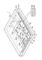
図1に示すように、有機EL表示装置1は、画像を表示する表示エリア102を有するアレイ基板100を備えて構成されている。表示エリア102は、マトリクス状に配置された複数の画素PX(R、G、B)によって構成されている。アレイ基板100の少なくとも表示エリア102は、封止体200によって密封されている。
As shown in FIG. 1, the organic
各画素PX(R、G、B)は、オン画素とオフ画素とを電気的に分離しかつオン画素への映像信号を保持する機能を有する画素スイッチ10と、画素スイッチ10を介して供給される映像信号に基づき自己発光素子(表示素子)に供給する駆動電流量を制御する駆動素子20と、一方の端子が駆動素子20のゲートと接続し、且つ駆動素子20のゲートとソースとの電位差を一定に保持する蓄積容量素子30とを備えている。これら画素スイッチ10及び駆動素子20は、例えばポリシリコン膜からなる半導体層を備えたPチャネル型薄膜トランジスタにより構成されている。
Each pixel PX (R, G, B) is supplied via a pixel switch 10 and a pixel switch 10 having a function of electrically separating an on-pixel and an off-pixel and holding a video signal to the on-pixel. A
また、各画素PX(R、G、B)は、自己発光素子としての有機EL素子40(R、G、B)をそれぞれ備えている。すなわち、赤色画素PXRは、赤色に発光する有機EL素子40Rを備え、緑色画素PXGは、緑色に発光する有機EL素子40Gを備え、さらに、青色画素PXBは、青色に発光する有機EL素子40Bを備えている。
Each pixel PX (R, G, B) includes an organic EL element 40 (R, G, B) as a self-light emitting element. That is, the red pixel PXR includes an organic EL element 40R that emits red light, the green pixel PXG includes an
各種有機EL素子40(R、G、B)は、基本的に同一構造である。すなわち、有機EL素子40は、マトリクス状に配置され画素毎PXに独立島状に形成された第1電極60と、第1電極60に対向して配置され全画素PXに共通に形成された第2電極66と、これら第1電極60と第2電極66との間に保持された有機活性層64と、によって構成される。
The various organic EL elements 40 (R, G, B) basically have the same structure. That is, the
第1電極60は、ここではITO(Indium Tin Oxide:インジウム・ティン・オキサイド)やIZO(インジウム・ジンク・オキサイド)などの光透過性導電部材によって形成され、陽極として機能する。
Here, the
有機活性層64は、少なくとも発光機能を有する有機化合物を含み、各色共通に形成されるホールバッファ層、エレクトロンバッファ層、及び各色毎に形成される有機発光層の3層積層で構成されても良く、機能的に複合された2層または単層で構成されても良い。例えば、ホールバッファ層は、陽極および有機発光層間に配置され、芳香族アミン誘導体やポリチオフェン誘導体、ポリアニリン誘導体などの薄膜によって形成される。有機発光層は、赤、緑、または青に発光する発光機能を有する有機化合物によって形成される。この有機発光層は、例えば高分子系の発光材料を採用する場合には、PPV(ポリパラフェニレンビニレン)やポリフルオレン誘導体またはその前駆体などの薄膜により構成される。
The organic
第2電極66は、例えばCa(カルシウム)、Al(アルミニウム)、Ba(バリウム)、Ag(銀)、Yb(イッテルビウム)などの電子注入機能を有する金属膜によって形成され、陰極として機能している。この第2電極66は、陰極として機能する金属膜の表面をカバーメタルで被覆した2層構造であっても良い。さらに、この第2電極66の表面は、乾燥剤として吸湿性を有する材料で被覆されてもよい。
The
アレイ基板100は、画素PXの行方向(すなわち図1のY方向)に沿って配置された複数の走査線Ym(m=1、2、…)と、走査線Ymと略直交する方向(すなわち図1のX方向)に沿って配置された複数の信号線Xn(n=1、2、…)と、有機EL素子40の第1電極60側に電源を供給するための電源供給線Pm(m=1、2、…)と、を備えている。電源供給線Pmは、表示エリア102の周囲に配置された図示しない第1電極電源線に接続されている。有機EL素子40の第2電極66側端は、表示エリア102の周囲に配置されコモン電位ここでは接地電位を供給する図示しない第2電極電源線に接続されている。
The
また、アレイ基板100は、表示エリア102の外周に沿った周辺エリア104に、走査線Ymに走査信号を供給する走査線駆動回路107と、信号線Xnに映像信号を供給する信号線駆動回路108と、を備えている。すべての走査線Ymは、走査線駆動回路107に接続されている。また、すべての信号線Xnは、信号線駆動回路108に接続されている。
The
画素スイッチ10は、ここでは走査線Ymと信号線Xnとの交差部近傍に配置されている。画素スイッチ10のゲート電極は走査線Ymに接続され、ソース電極は信号線Xnに接続され、ドレイン電極は蓄積容量素子30を構成する一方の電極及び駆動素子20のゲート電極に接続されている。駆動素子20のソース電極は電源供給線Pmに接続され、またここでは駆動素子20のソース電極は蓄積容量素子30を構成する他方の電極に接続され、ドレイン電極は有機EL素子40の第1電極60に接続されている。
Here, the pixel switch 10 is disposed in the vicinity of the intersection between the scanning line Ym and the signal line Xn. The gate electrode of the pixel switch 10 is connected to the scanning line Ym, the source electrode is connected to the signal line Xn, and the drain electrode is connected to one electrode constituting the
このように構成された有機EL表示装置1では、各画素PXの有機EL素子40において、第1電極60と第2電極66との間に挟持された有機活性層64に電子及びホールを注入し、これらを再結合させることにより励起子を生成し、この励起子の失活時に生じる所定波長の光放出により発光する。このときに発生したEL発光は、アレイ基板100の下面側すなわち第1電極60側から出射される(下面発光方式)、あるいは、アレイ基板100の上面側すなわち第2電極66側から出射される(上面発光方式)。
In the organic
ところで、各画素PXに配置された駆動素子20は、図2に示すように、ポリシリコン膜によって形成された半導体層21を有している。この半導体層21は、アレイ基板を構成するガラスなどの絶縁性基板110上あるいは窒化膜や酸化膜などのアンダーコーティング層上に配置されている。また、この半導体層21は、チャネル領域21Cの両側にそれぞれ不純物をドープすることによって形成されたドレイン領域21D及びソース領域21Sを有している。このような半導体層21は、ゲート絶縁膜111によって覆われている。
Incidentally, the
駆動素子20のゲート電極22は、ゲート絶縁膜111を介して半導体層21のチャネル領域21Cの真上に位置して配置されている。このようなゲート電極22は、層間絶縁膜112によって覆われている。
The
駆動素子20のドレイン電極23Dは、ゲート絶縁膜111及び層間絶縁膜112を貫通するコンタクトホール113を介して半導体層21のドレイン領域21Dに電気的に接続されている。駆動素子20のソース電極23Sは、ゲート絶縁膜111及び層間絶縁膜112を貫通するコンタクトホール114を介して半導体層21のソース領域21Sに電気的に接続されている。
The drain electrode 23 </ b> D of the driving
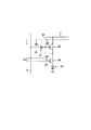
チャネル領域21Cは、図3及び図4に示すように、ソース領域21Sとドレイン領域21Dとを繋ぐ少なくとも2つの伝導領域C1、C2…を備えている。すなわち、これら伝導領域C(1、2…)のそれぞれは、アモルファスシリコン膜に対してレーザビームをパルス照射してアニールすることによって多結晶化し、レーザビームによる異なるショットで最終形成された少なくとも2つの多結晶領域によって形成されている。
As shown in FIGS. 3 and 4, the
チャネル領域21Cを構成するシリコン結晶の粒径(結晶性)は、最終的に照射されたレーザビームによるショットで決まる。このため、各多結晶領域を形成する際に最終的に照射されたレーザビームのパワーにバラツキが生じた場合、各伝導領域C(1、2…)を構成するシリコンの結晶性が互いに異なる。つまり、チャネル領域21Cは、ソース領域21Sとドレイン領域21Dとを繋ぐ平均粒径の異なる少なくとも2つの伝導領域C(1、2…)を備えることになる。
The grain size (crystallinity) of the silicon crystal constituting the
このようなチャネル領域21Cに含まれる各伝導領域C(1、2…)は、ソース領域21Sとドレイン領域21Dとを繋ぐような形状であれば良い。
Each conductive region C (1, 2,...) Included in such a
例えば、図3に示すように、各伝導領域C(1、2…)は、チャネル領域21Cの長さ方向(あるいは半導体層21が延在する方向)Aに沿って延びた形状であって、それぞれの伝導領域C(1、2…)は、互いにソース・ドレイン方向に沿って並列に形成しても良い。この場合、隣接する2つの伝導領域C1とC2との間の境界21Bは、チャネル領域21Cの長さ方向Aに対してほぼ平行である。
For example, as shown in FIG. 3, each conductive region C (1, 2,...) Has a shape extending along the length direction A (or the direction in which the
また、図4に示すように、各伝導領域C(1、2…)は、チャネル領域21Cの長さ方向(あるいは半導体層21が延在する方向)Aに対して非平行な方向に沿って延びた形状であっても良い。この場合、隣接する2つの伝導領域C1とC2との間の境界21Bは、チャネル領域21Cの長さ方向Aに対して斜めである。
Further, as shown in FIG. 4, each conduction region C (1, 2,...) Is along a direction that is not parallel to the length direction A (or the direction in which the
このような構成とすることにより、各伝導領域を形成するための多結晶領域毎にシリコンの結晶性が異なったとしても、チャネル領域21C内に複数の移動度を有する伝導領域C(1、2…)を備えることになり、チャネル領域21C全体での移動度を平均化することができる。このため、駆動素子20による有機EL素子40への駆動電流の供給能力を平均化することができる。これにより、同一レベルの映像信号で各有機EL素子40を発光させようとした場合、駆動素子20間での電流供給能力のバラツキを改善することができる。したがって、均一な画面を表示させた場合、画素間の輝度差を低減することができ、表示品位を向上することが可能となる。
With such a configuration, even if the crystallinity of silicon differs for each polycrystalline region for forming each conductive region, the conductive region C (1, 2) having a plurality of mobilities in the
なお、図5に示すように、チャネル領域21Cに含まれる各伝導領域C(1、2…)がソース領域21Sとドレイン領域21Dとを繋ぐような形状とならない、つまり、各伝導領域C(1、2…)がチャネル領域21Cの長さ方向Aに対してほぼ直交する形状となることは望ましくない。すなわち、図5に示すような形状の伝導領域C(1、2…)のうち、シリコンの結晶性の差異により1領域でも移動度の小さい領域が形成されてしまうと、ソース−ドレイン間で抵抗律速されることになる。
As shown in FIG. 5, the conductive regions C (1, 2,...) Included in the
つまり、シリコンの結晶性が異なった場合、駆動素子20による電流供給能力を平均化するどころか、むしろ駆動素子間での電流供給能力のバラツキを増大させてしまうことになる。このため、チャネル領域21Cは、ソース領域21Sとドレイン領域21Dとを繋ぐ少なくとも2つの伝導領域C(1、2…)を備えることが必要となる。
In other words, when the crystallinity of silicon is different, the current supply capability of the
次に、上述した表示装置の製造方法について説明する。ここでは、駆動素子20の半導体層21を形成する第1の製造方法について説明する。
Next, a method for manufacturing the display device described above will be described. Here, a first manufacturing method for forming the
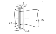
まず、アモルファスシリコン膜a−Siを成膜した基板を用意する。そして、図6に示すように、成膜されたアモルファスシリコン膜a−Siに対して、レーザビームを所定スキャン方向(ショットの移動方向)Bに沿ってずらしながらパルス照射する。このとき、レーザビームの熱エネルギによりアモルファスシリコンを加熱して一旦溶融した後に、再結晶化することで多結晶化する。これにより、ポリシリコン膜p−Siを形成する。 First, a substrate on which an amorphous silicon film a-Si is formed is prepared. Then, as shown in FIG. 6, the amorphous silicon film a-Si thus formed is irradiated with pulses while shifting the laser beam along a predetermined scanning direction (shot moving direction) B. At this time, the amorphous silicon is heated by the thermal energy of the laser beam and once melted, and then recrystallized to be polycrystallized. Thereby, a polysilicon film p-Si is formed.
なお、このようなレーザアニール工程では、アモルファスシリコン膜a−Siのすべてのエリアは、ほぼ同一の熱エネルギで加熱される。すなわち、レーザビームは、スキャン方向Bを短手とし、スキャン方向Bと直交する方向を長手とするほぼ矩形状のビーム断面を有している。このようなビーム断面を有するレーザビームは、スキャン方向Bに沿って所定ピッチLPでずらしながら照射される。 In such a laser annealing process, all areas of the amorphous silicon film a-Si are heated with substantially the same thermal energy. That is, the laser beam has a substantially rectangular beam cross section in which the scanning direction B is short and the direction orthogonal to the scanning direction B is long. The laser beam having such a beam cross section is irradiated while being shifted at a predetermined pitch LP along the scanning direction B.
これにより、図7に示すように、ポリシリコン膜p−Siは、最終的に照射されたレーザビームによるnショットで最終形成された多結晶領域N、同様に、最終的に照射されたレーザビームによる(n+1)ショットで最終形成された多結晶領域(N+1)、最終的に照射されたレーザビームによる(n+2)ショットで最終形成された多結晶領域(N+2)…を有することになる。各多結晶領域の幅NWは、レーザビームの所定ピッチLPに対応する。また、各多結晶領域の幅方向は、レーザビームの所定スキャン方向Bに一致しする。 As a result, as shown in FIG. 7, the polysilicon film p-Si is formed in the polycrystalline region N finally formed by the n shot by the finally irradiated laser beam, and similarly, the finally irradiated laser beam. The polycrystalline region (N + 1) finally formed by the (n + 1) shot of (n + 1), the polycrystalline region (N + 2)... Finally formed by the (n + 2) shot by the finally irradiated laser beam. The width NW of each polycrystalline region corresponds to a predetermined pitch LP of the laser beam. The width direction of each polycrystalline region coincides with a predetermined scanning direction B of the laser beam.
例えば、レーザビームのスキャン方向Bに沿った幅LWを例えば100μmとし、所定ピッチLPを5μmとすると、すべてのエリアは20ショットのレーザビームが照射されることになる。つまり、多結晶領域Nは、(n−19)ショットからnショットまで連続する20ショットのレーザビームが照射される。 For example, if the width LW along the scanning direction B of the laser beam is, for example, 100 μm and the predetermined pitch LP is 5 μm, all areas are irradiated with 20 shots of the laser beam. That is, the polycrystalline region N is irradiated with a laser beam of 20 shots continuous from (n-19) shots to n shots.
レーザビームによるスキャンは、固定された基板に対してレーザビームの照射位置を所定ピッチで移動することによって行っても良いし、一定速度で連続的に移動する基板に対して所定間隔でレーザビームを照射することによって行っても良い。特に、後者の方法によれば、レーザビームの照射タイミングが所定間隔で維持できれば、特に位置合わせなど手間がなく、レーザアニール工程の効率を改善することができる。 Scanning with a laser beam may be performed by moving the irradiation position of the laser beam at a predetermined pitch with respect to a fixed substrate, or the laser beam may be emitted at a predetermined interval with respect to a substrate that moves continuously at a constant speed. You may carry out by irradiating. In particular, according to the latter method, if the irradiation timing of the laser beam can be maintained at a predetermined interval, the efficiency of the laser annealing process can be improved without any trouble such as alignment.
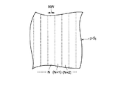
続いて、図8に示すように、ポリシリコン膜p−Siをパターニングする。このとき、特に、レーザビームによる異なるショットで最終形成された少なくとも2つの多結晶領域N、(N+1)…を含むようにポリシリコン膜p−Siをパターニングする。すなわち、このパターニング工程では、隣接する2つの多結晶領域N及び(N+1)の少なくとも一部を含むような形状にポリシリコン膜をパターン化すればよい。 Subsequently, as shown in FIG. 8, the polysilicon film p-Si is patterned. At this time, in particular, the polysilicon film p-Si is patterned so as to include at least two polycrystalline regions N, (N + 1)... Finally formed by different shots with a laser beam. That is, in this patterning step, the polysilicon film may be patterned into a shape including at least a part of two adjacent polycrystalline regions N and (N + 1).
また、レーザビームの所定ピッチLPすなわち多結晶領域の幅NWよりも大きな所定幅CWを有するようにポリシリコン膜p−Siをパターニングしても良い。このような所定幅CWを選んでパターニングすることにより、パターン化されたポリシリコン膜p−Siは、確実に少なくとも2つの多結晶領域N、(N+1)…を含むことになる。 Alternatively, the polysilicon film p-Si may be patterned so as to have a predetermined width LP of the laser beam, that is, a predetermined width CW larger than the width NW of the polycrystalline region. By selecting and patterning such a predetermined width CW, the patterned polysilicon film p-Si surely includes at least two polycrystalline regions N, (N + 1).
望ましくは、多結晶領域の幅NW(レーザビームの所定ピッチLP)が所定幅CW(チャネル領域21の幅に相当)の1/2以下のできるだけ小さい値となるように設定する。これにより、パターン化されたポリシリコン膜p−Siは、確実に2つ以上の多結晶領域N、(N+1)…を含むことになる。 Desirably, the width NW (predetermined pitch LP of the laser beam) of the polycrystalline region is set to be as small as possible not more than 1/2 of the predetermined width CW (corresponding to the width of the channel region 21). As a result, the patterned polysilicon film p-Si surely includes two or more polycrystalline regions N, (N + 1).
例えば、各多結晶領域N、(N+1)…の幅NWを5μmとし、15μmの所定幅CWでポリシリコン膜p−Siをパターニングすることにより、図8に示すように、パターン化されたポリシリコン膜p−Siは、3つ以上の多結晶領域N、(N+1)、(n+2)を含むことになる。 For example, by setting the width NW of each polycrystalline region N, (N + 1)... To 5 .mu.m and patterning the polysilicon film p-Si with a predetermined width CW of 15 .mu.m, as shown in FIG. The film p-Si includes three or more polycrystalline regions N, (N + 1), and (n + 2).
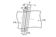
続いて、図9に示すように、ポリシリコン膜p−Siにチャネル領域21Cを挟んだ両側にソース領域21S及びドレイン領域21Dをそれぞれ形成することによって半導体層21を形成する。すなわち、パターン化されたポリシリコン膜p−Siをゲート絶縁膜で覆った後、ポリシリコン膜p−Siのほぼ中央に重なるようにゲート電極22を形成し、さらに、このゲート電極22をマスクとしてポリシリコン膜p−Siに不純物をドープする。
Subsequently, as shown in FIG. 9, the
これにより、ゲート電極22と重ならないポリシリコン膜p−Siの両側、すなわちチャネル領域21Cを挟んでレーザビームの所定スキャン方向Bとほぼ直交する両側に、それぞれソース領域21S及びドレイン領域21Dが形成される。
As a result, the
また、チャネル領域21Cは、複数の多結晶領域N、(N+1)…によって形成された複数の伝導領域C1、C2…を備える。これら伝導領域C1、C2…のそれぞれは、ソース領域21Sとドレイン領域21Dとを繋ぐように形成される。この伝導領域C1は、レーザビームによるnショットで最終形成された多結晶領域Nによって形成される。同様に、伝導領域C2は、レーザビームによるnショットに続く(n+1)ショットで最終形成された多結晶領域(N+1)によって形成される。
Further, the
チャネル領域21C内にこれらの複数の伝導領域C1、C2…を形成するためには、レーザビームのスキャン方向Bがチャネル領域21Cの幅CWを規定する幅方向と非直交であることが必要であり、この第1の製造方法では、スキャン方向Bを幅方向と平行としている。
In order to form the plurality of conductive regions C1, C2,... In the
このような第1の製造方法によれば、レーザアニール工程でのレーザビームのショット間にパワーのバラツキが生じても、各伝導領域を形成する多結晶領域毎にシリコンの結晶性が異なってしまうが、チャネル領域21C内に複数の移動度を有する伝導領域C(1、2…)を備えることにより、チャネル領域21C全体での移動度を平均化することができる。このため、駆動素子20による有機EL素子40への駆動電流の供給能力を平均化することができる。これにより、同一レベルの映像信号で各有機EL素子40を発光させようとした場合、均一な画面を表示させることができ、表示品位を向上することが可能となる。
According to such a first manufacturing method, even if power variation occurs between shots of the laser beam in the laser annealing step, the crystallinity of silicon differs for each polycrystalline region forming each conductive region. However, by providing the conductive regions C (1, 2,...) Having a plurality of mobility in the
また、レーザビームによる異なるショットで最終形成された少なくとも2つの多結晶領域N、(N+1)…を含むようにポリシリコン膜p−Siをパターニングすればよいが、レーザビームの所定ピッチLPよりも大きな所定幅CWを有するようにポリシリコン膜をパターニングすることで、チャネル領域21Cは、少なくとも2つの伝導領域C1、C2…を含むことになる。また、レーザビームの所定ピッチLPをチャネル領域21の幅CWの1/2以下とすることで、チャネル領域21Cは、確実に2つ以上の伝導領域C1、C2…を含むことになる。このため、各伝導領域での移動度が異なったとしても、チャネル領域21C全体での移動度をより平均化することができる。
Further, the polysilicon film p-Si may be patterned so as to include at least two polycrystalline regions N, (N + 1)... Finally formed by different shots by the laser beam, but larger than the predetermined pitch LP of the laser beam. By patterning the polysilicon film so as to have a predetermined width CW, the
次に、駆動素子20の半導体層21を形成する第2の製造方法について説明する。なお、第1の製造方法と同一工程については詳細な説明を省略する。
Next, a second manufacturing method for forming the
まず、アモルファスシリコン膜a−Siを成膜した基板を用意する。そして、図10に示すように、成膜されたアモルファスシリコン膜a−Siに対して、レーザビームを所定スキャン方向(ショットの移動方向)Bに沿って所定ピッチLPでずらしながらパルス照射する。 First, a substrate on which an amorphous silicon film a-Si is formed is prepared. Then, as shown in FIG. 10, the amorphous silicon film a-Si thus formed is irradiated with pulses while shifting the laser beam at a predetermined pitch LP along a predetermined scanning direction (shot moving direction) B.
これにより形成されたポリシリコン膜p−Siは、図11に示すように、最終的に照射されたレーザビームによるnショットで最終形成された多結晶領域N、同様に、最終的に照射されたレーザビームによる(n+1)ショットで最終形成された多結晶領域(N+1)、最終的に照射されたレーザビームによる(n+2)ショットで最終形成された多結晶領域(N+2)…を有することになる。各多結晶領域の幅NWは、レーザビームの所定ピッチLPに対応する。また、各多結晶領域の幅方向は、レーザビームの所定スキャン方向Bに一致しする。 As shown in FIG. 11, the polysilicon film p-Si thus formed is finally irradiated with the polycrystalline region N finally formed by the n shot by the finally irradiated laser beam. The polycrystalline region (N + 1) finally formed by the (n + 1) shot by the laser beam, the polycrystalline region (N + 2) finally formed by the (n + 2) shot by the finally irradiated laser beam. The width NW of each polycrystalline region corresponds to a predetermined pitch LP of the laser beam. The width direction of each polycrystalline region coincides with a predetermined scanning direction B of the laser beam.
続いて、図12に示すように、ポリシリコン膜p−Siをパターニングする。このとき、特に、レーザビームによる異なるショットで最終形成された少なくとも2つの多結晶領域N、(N+1)…を含むようにポリシリコン膜p−Siをパターニングする。 Subsequently, as shown in FIG. 12, the polysilicon film p-Si is patterned. At this time, in particular, the polysilicon film p-Si is patterned so as to include at least two polycrystalline regions N, (N + 1)... Finally formed by different shots with a laser beam.
また、レーザビームの所定ピッチLPすなわち多結晶領域の幅NWよりも大きな所定幅CWを有するようにポリシリコン膜p−Siをパターニングしても良い。このような所定幅CWを選んでパターニングすることにより、パターン化されたポリシリコン膜p−Siは、確実に少なくとも2つの多結晶領域N、(N+1)…を含むことになる。 Alternatively, the polysilicon film p-Si may be patterned so as to have a predetermined width LP of the laser beam, that is, a predetermined width CW larger than the width NW of the polycrystalline region. By selecting and patterning such a predetermined width CW, the patterned polysilicon film p-Si surely includes at least two polycrystalline regions N, (N + 1).
望ましくは、多結晶領域の幅NW(レーザビームの所定ピッチLP)が所定幅CW(チャネル領域21の幅に相当)の1/2以下のできるだけ小さい値となるように設定する。これにより、パターン化されたポリシリコン膜p−Siは、確実に2つ以上の多結晶領域N、(N+1)…を含むことになる。 Desirably, the width NW (predetermined pitch LP of the laser beam) of the polycrystalline region is set to be as small as possible not more than 1/2 of the predetermined width CW (corresponding to the width of the channel region 21). As a result, the patterned polysilicon film p-Si surely includes two or more polycrystalline regions N, (N + 1).
続いて、図13に示すように、ポリシリコン膜p−Siにチャネル領域21Cを挟んだ両側にソース領域21S及びドレイン領域21Dをそれぞれ形成することによって半導体層21を形成する。すなわち、パターン化されたポリシリコン膜p−Siをゲート絶縁膜で覆った後、ポリシリコン膜p−Siのほぼ中央に重なるようにゲート電極22を形成し、さらに、このゲート電極22をマスクとしてポリシリコン膜p−Siに不純物をドープする。
Subsequently, as shown in FIG. 13, the
これにより、ゲート電極22と重ならないポリシリコン膜p−Siの両側、すなわちチャネル領域21Cを挟んでレーザビームの所定スキャン方向Bとほぼ直交する両側に、それぞれソース領域21S及びドレイン領域21Dが形成される。
As a result, the
また、チャネル領域21Cは、複数の多結晶領域N、(N+1)…によって形成された複数の伝導領域C1、C2…を備える。これら伝導領域C1、C2…のそれぞれは、ソース領域21Sとドレイン領域21Dとを繋ぐように形成される。この伝導領域C1は、レーザビームによるnショットで最終形成された多結晶領域Nによって形成される。同様に、伝導領域C2は、レーザビームによるnショットに続く(n+1)ショットで最終形成された多結晶領域(N+1)によって形成される。
Further, the
チャネル領域21C内にこれらの複数の伝導領域C1、C2…を形成するためには、レーザビームのスキャン方向Bがチャネル領域21Cの幅CWを規定する幅方向と非直交であることが必要であり、この第2の製造方法では、スキャン方向Bを幅方向に対して斜めの方向としている。
In order to form the plurality of conductive regions C1, C2,... In the
このような第2の製造方法によれば、上述した第1の製造方法による効果に加えて、駆動素子の各画素内における位置を同一とした場合、表示エリアの行方向及び列方向に並んだ各画素の駆動素子が同一ショットで最終形成されたポリシリコン膜を有することがない。つまり、表示エリアの斜め方向に並んだ各画素の駆動素子が同一ショットで最終形成されたポリシリコン膜を有することになる。このため、第1の製造方法による駆動素子よりも表示エリアの行方向及び列方向に延びるスジ状の輝度ムラを視認しにくくすることができる。 According to such a second manufacturing method, in addition to the effects of the first manufacturing method described above, when the positions of the drive elements in each pixel are the same, the display areas are arranged in the row direction and the column direction. The drive element of each pixel does not have a polysilicon film finally formed in the same shot. That is, the drive elements of the pixels arranged in the oblique direction of the display area have the polysilicon film finally formed in the same shot. For this reason, streaky luminance unevenness extending in the row direction and the column direction of the display area can be made harder to visually recognize than the driving element according to the first manufacturing method.
ところで、カラー有機EL表示装置の場合、表示色によって人間の目の視認度が異なる。例えば、上述した実施の形態のように、赤色画素PXR、緑色画素PXB、及び、青色画素PXBによってカラー表示を実現する場合、緑色の視認度が他の表示色に比べて高い。このため、緑色画素について(緑色画面を表示した場合)、特に輝度ムラが視認されやすい。 By the way, in the case of a color organic EL display device, the visibility of human eyes varies depending on the display color. For example, when the color display is realized by the red pixel PXR, the green pixel PXB, and the blue pixel PXB as in the above-described embodiment, the green visibility is higher than the other display colors. For this reason, luminance unevenness is particularly easily observed with respect to green pixels (when a green screen is displayed).
そこで、緑色画素(第1色用画素)については、半導体層21におけるチャネル領域21Cの幅CWと各伝導領域C1、C2…の幅NWとの商が、他の色すなわち赤色画素及び青色画素(第2色用画素)と異なるように設定することが望ましい。
Therefore, for the green pixel (first color pixel), the quotient of the width CW of the
例えば、緑色画素の半導体層21におけるチャネル領域21Cの幅CWに対して各伝導領域の幅NWを(CW/3)以下とし、このときの赤色画素及び青色画素の半導体層21におけるチャネル領域21Cの幅CWに対して各伝導領域の幅NWを(CW/2)以下とする。このような構成は、青色画素の半導体層を形成するためのレーザビームの所定ピッチを他の色の場合よりも小さくする、あるいは、青色画素の半導体層の幅(チャネル領域の幅)を他の色の場合よりも大きくするなどの方法で実現可能である。
For example, the width NW of each conductive region is set to (CW / 3) or less with respect to the width CW of the
これにより、緑色画素についてはチャネル領域に3つ以上の伝導領域が形成され、他の色の画素についてはチャネル領域に2つ以上の伝導領域が形成されることになる。つまり、緑色画素について、チャネル領域全体での移動度のバラツキを他の色よりもさらに平均化することができる。このため、視認度の高い色(例えば緑色)について、輝度ムラを改善することができる。 As a result, three or more conductive regions are formed in the channel region for the green pixel, and two or more conductive regions are formed in the channel region for the other color pixels. That is, for the green pixel, the variation in mobility in the entire channel region can be averaged more than other colors. For this reason, luminance unevenness can be improved for a color with high visibility (for example, green).
なお、この発明は、図1に示したような回路構成の駆動素子にのみ適用されるものではない。例えば、図14に示すように、駆動素子20の特性を揃えるために、しきい値ばらつきをキャンセルするために組み込まれた回路を備えていても良い。すなわち、この回路構成では、画素スイッチ10と蓄積容量素子30との間にしきい値ばらつきキャンセル容量素子31を備え、さらに、制御配線32に接続された2つのしきい値ばらつきキャンセル動作制御用の制御素子33及び34を備えている。
The present invention is not applied only to drive elements having a circuit configuration as shown in FIG. For example, as shown in FIG. 14, in order to make the characteristics of the
このような回路構成においても、画素スイッチ10、駆動素子20、制御素子33及び34がポリシリコン膜からなる半導体層を備えた薄膜トランジスタによって構成された場合、移動度のばらつきについては完全にキャンセルできないという問題がある。そこで、駆動素子20の半導体層を上述したような構成とすることにより、移動度のバラツキを平均化することができる。
Even in such a circuit configuration, when the pixel switch 10, the
以上説明したように、有機EL素子40に駆動電流を供給する駆動素子20のチャネル領域の向き(長さ方向)Aをレーザビームのスキャン方向(ショット移動方向)Bに対して垂直な方向とし、しかも、チャネル領域をソース領域とドレイン領域とを繋ぐ複数の伝導領域C(1、2…)によって構成する。
As described above, the direction (length direction) A of the channel region of the
このとき、各伝導領域C(1、2…)にてシリコン結晶の平均粒径が異なる場合、各伝導領域C(1、2…)が互いにソース・ドレイン方向に沿って並列に形成されているため、移動度が律速されることはない。このため、駆動素子20による有機EL素子40への駆動電流の供給能力を平均化することができる。これにより、均一な画面を表示させた場合、画素間の輝度差を低減することができ、表示品位を向上することが可能となる。
At this time, when the average grain size of the silicon crystal is different in each conductive region C (1, 2,...), Each conductive region C (1, 2,...) Is formed in parallel along the source / drain direction. Therefore, the mobility is not limited. For this reason, it is possible to average the drive current supply capability of the
なお、この発明は、上記実施形態そのままに限定されるものではなく、その実施の段階ではその要旨を逸脱しない範囲で構成要素を変形して具体化できる。また、上記実施形態に開示されている複数の構成要素の適宜な組み合せにより種々の発明を形成できる。例えば、実施形態に示される全構成要素から幾つかの構成要素を削除してもよい。更に、異なる実施形態に亘る構成要素を適宜組み合せてもよい。 Note that the present invention is not limited to the above-described embodiment as it is, and can be embodied by modifying the constituent elements without departing from the spirit of the invention in the stage of implementation. Further, various inventions can be formed by appropriately combining a plurality of constituent elements disclosed in the embodiment. For example, some components may be deleted from all the components shown in the embodiment. Furthermore, you may combine suitably the component covering different embodiment.
1…有機EL表示装置、10…画素スイッチ、20…駆動素子、21…半導体層、21C…チャネル領域、21S…ソース領域、21D…ドレイン領域、22…ゲート電極、23S…ソース電極、23D…ドレイン電極、30…蓄積容量素子、40…有機EL素子、100…アレイ基板、PX…画素、C…伝導領域、N…多結晶領域、n…ショット
DESCRIPTION OF
Claims (15)
基板上に成膜されたアモルファスシリコン膜に対して、レーザビームを所定スキャン方向に沿ってずらしながらパルス照射してポリシリコン膜を形成し、
レーザビームによる異なるショットで最終形成された少なくとも2つの多結晶領域を含むように前記ポリシリコン膜をパターニングし、
前記ポリシリコン膜にチャネル領域を挟んだ両側にソース領域及びドレイン領域をそれぞれ形成することによって前記半導体層を形成するものであって、
前記チャネル領域は、複数の前記多結晶領域によって形成され前記ソース領域と前記ドレイン領域とを繋ぐ複数の伝導領域を備えたことを特徴とする表示装置の製造方法。 A method of manufacturing a display device for forming a semiconductor layer of a drive element that controls a drive current amount supplied to a self-light emitting element,
The amorphous silicon film formed on the substrate is irradiated with pulses while shifting the laser beam along a predetermined scanning direction to form a polysilicon film,
Patterning the polysilicon film to include at least two polycrystalline regions finally formed in different shots with a laser beam;
Forming the semiconductor layer by forming a source region and a drain region on both sides of a channel region in the polysilicon film,
The method for manufacturing a display device, wherein the channel region includes a plurality of conductive regions formed by a plurality of the polycrystalline regions and connecting the source region and the drain region.
基板上に成膜されたアモルファスシリコン膜に対して、レーザビームを所定スキャン方向に沿って所定ピッチでずらしながらパルス照射してポリシリコン膜を形成し、
前記所定ピッチよりも大きな所定幅を有するように前記ポリシリコン膜をパターニングし、
前記ポリシリコン膜にチャネル領域を挟んで前記所定スキャン方向とほぼ直交する両側にソース領域及びドレイン領域をそれぞれ形成することを特徴とする表示装置の製造方法。 A method of manufacturing a display device for forming a semiconductor layer of a drive element that controls a drive current amount supplied to a self-light emitting element,
The amorphous silicon film formed on the substrate is irradiated with pulses while shifting the laser beam at a predetermined pitch along a predetermined scanning direction to form a polysilicon film,
Patterning the polysilicon film to have a predetermined width larger than the predetermined pitch;
A method of manufacturing a display device, wherein a source region and a drain region are formed on both sides substantially orthogonal to the predetermined scanning direction with a channel region sandwiched between the polysilicon films.
しかも、第1伝導領域はレーザビームによる第1ショットで最終形成された第1多結晶領域によって形成され、第2伝導領域は前記第1ショットに続く第2ショットで最終形成された第2多結晶領域によって形成されたことを特徴とする請求項5に記載の表示装置の製造方法。 The channel region includes at least two conductive regions that connect the source region and the drain region,
In addition, the first conductive region is formed by the first polycrystalline region finally formed by the first shot by the laser beam, and the second conductive region is the second polycrystalline layer finally formed by the second shot following the first shot. 6. The method for manufacturing a display device according to claim 5, wherein the display device is formed by a region.
前記画素の各々は、自己発光素子と、前記自己発光素子に供給する駆動電流量を制御する駆動素子と、を備え、
前記駆動素子は、ポリシリコン膜からなる半導体層を備えた薄膜トランジスタにより構成され、
前記半導体層におけるソース領域とドレイン領域との間のチャネル領域は、前記ソース領域と前記ドレイン領域とを繋ぐ平均粒径の異なる少なくとも2つの伝導領域を備えたことを特徴とする表示装置。 A display device having a display area composed of a plurality of pixels arranged in a matrix,
Each of the pixels includes a self-light-emitting element and a drive element that controls the amount of drive current supplied to the self-light-emitting element,
The driving element is constituted by a thin film transistor including a semiconductor layer made of a polysilicon film,
A display device, wherein a channel region between a source region and a drain region in the semiconductor layer includes at least two conductive regions having different average particle diameters connecting the source region and the drain region.
前記伝導領域のそれぞれは、レーザビームによる異なるショットで最終形成されたことを特徴とする請求項11に記載の表示装置。 The semiconductor layer is formed by annealing a pulsed laser beam on the amorphous silicon film,
The display device according to claim 11, wherein each of the conductive regions is finally formed by a different shot by a laser beam.
Priority Applications (6)
| Application Number | Priority Date | Filing Date | Title |
|---|---|---|---|
| JP2003398085A JP2005159162A (en) | 2003-11-27 | 2003-11-27 | Display device and its manufacturing method |
| KR1020040077809A KR100693235B1 (en) | 2003-11-27 | 2004-09-30 | Display device and manufacturing method thereof |
| TW093129637A TWI266921B (en) | 2003-11-27 | 2004-09-30 | Display device and manufacturing method |
| SG200407601A SG112108A1 (en) | 2003-11-27 | 2004-11-25 | Display device and method of manufacturing the same |
| US10/996,409 US7084081B2 (en) | 2003-11-27 | 2004-11-26 | Display device and method of manufacturing the same |
| CNB2004100974912A CN100372054C (en) | 2003-11-27 | 2004-11-29 | Display device and method of manufacturing the same |
Applications Claiming Priority (1)
| Application Number | Priority Date | Filing Date | Title |
|---|---|---|---|
| JP2003398085A JP2005159162A (en) | 2003-11-27 | 2003-11-27 | Display device and its manufacturing method |
Publications (2)
| Publication Number | Publication Date |
|---|---|
| JP2005159162A true JP2005159162A (en) | 2005-06-16 |
| JP2005159162A5 JP2005159162A5 (en) | 2006-12-28 |
Family
ID=34723053
Family Applications (1)
| Application Number | Title | Priority Date | Filing Date |
|---|---|---|---|
| JP2003398085A Pending JP2005159162A (en) | 2003-11-27 | 2003-11-27 | Display device and its manufacturing method |
Country Status (6)
| Country | Link |
|---|---|
| US (1) | US7084081B2 (en) |
| JP (1) | JP2005159162A (en) |
| KR (1) | KR100693235B1 (en) |
| CN (1) | CN100372054C (en) |
| SG (1) | SG112108A1 (en) |
| TW (1) | TWI266921B (en) |
Cited By (2)
| Publication number | Priority date | Publication date | Assignee | Title |
|---|---|---|---|---|
| JP2007012815A (en) * | 2005-06-29 | 2007-01-18 | Kyodo Printing Co Ltd | Flexible display and its manufacturing method |
| JP2010541250A (en) * | 2007-09-25 | 2010-12-24 | ザ トラスティーズ オブ コロンビア ユニヴァーシティ イン ザ シティ オブ ニューヨーク | Method for producing high uniformity in thin film transistor devices fabricated on laterally crystallized thin films |
Families Citing this family (3)
| Publication number | Priority date | Publication date | Assignee | Title |
|---|---|---|---|---|
| US7187123B2 (en) * | 2004-12-29 | 2007-03-06 | Dupont Displays, Inc. | Display device |
| KR100703467B1 (en) * | 2005-01-07 | 2007-04-03 | 삼성에스디아이 주식회사 | Thin Film Transistor |
| KR101293566B1 (en) * | 2007-01-11 | 2013-08-06 | 삼성디스플레이 주식회사 | Organic light emitting diode display and method for manufacturing the same |
Citations (2)
| Publication number | Priority date | Publication date | Assignee | Title |
|---|---|---|---|---|
| JP2001109399A (en) * | 1999-10-04 | 2001-04-20 | Sanyo Electric Co Ltd | Color display device |
| JP2002353140A (en) * | 2001-03-22 | 2002-12-06 | Sharp Corp | Semiconductor device and its fabricating method |
Family Cites Families (9)
| Publication number | Priority date | Publication date | Assignee | Title |
|---|---|---|---|---|
| JP3221473B2 (en) * | 1994-02-03 | 2001-10-22 | 株式会社半導体エネルギー研究所 | Method for manufacturing semiconductor device |
| JPH11121751A (en) | 1997-10-13 | 1999-04-30 | Sanyo Electric Co Ltd | Manufacture of thin-film semiconductor device |
| KR100292048B1 (en) * | 1998-06-09 | 2001-07-12 | 구본준, 론 위라하디락사 | Manufacturing Method of Thin Film Transistor Liquid Crystal Display |
| JP2000243968A (en) | 1999-02-24 | 2000-09-08 | Matsushita Electric Ind Co Ltd | Thin film transistor, manufacture thereof, liquid crystal display device using the same and manufacture thereof |
| JP2000243969A (en) | 1999-02-24 | 2000-09-08 | Matsushita Electric Ind Co Ltd | Thin film transistor, manufacture thereof, liquid crystal display device using the same and manufacture thereof |
| US6479837B1 (en) * | 1998-07-06 | 2002-11-12 | Matsushita Electric Industrial Co., Ltd. | Thin film transistor and liquid crystal display unit |
| JP2000133807A (en) | 1998-10-22 | 2000-05-12 | Seiko Epson Corp | Polycrystalline silicon thin-film transistor |
| JP5030345B2 (en) * | 2000-09-29 | 2012-09-19 | 三洋電機株式会社 | Semiconductor device |
| JP2004119919A (en) * | 2002-09-30 | 2004-04-15 | Hitachi Ltd | Semiconductor thin film and method for manufacturing the same |
-
2003
- 2003-11-27 JP JP2003398085A patent/JP2005159162A/en active Pending
-
2004
- 2004-09-30 TW TW093129637A patent/TWI266921B/en not_active IP Right Cessation
- 2004-09-30 KR KR1020040077809A patent/KR100693235B1/en not_active IP Right Cessation
- 2004-11-25 SG SG200407601A patent/SG112108A1/en unknown
- 2004-11-26 US US10/996,409 patent/US7084081B2/en active Active
- 2004-11-29 CN CNB2004100974912A patent/CN100372054C/en not_active Expired - Fee Related
Patent Citations (2)
| Publication number | Priority date | Publication date | Assignee | Title |
|---|---|---|---|---|
| JP2001109399A (en) * | 1999-10-04 | 2001-04-20 | Sanyo Electric Co Ltd | Color display device |
| JP2002353140A (en) * | 2001-03-22 | 2002-12-06 | Sharp Corp | Semiconductor device and its fabricating method |
Cited By (3)
| Publication number | Priority date | Publication date | Assignee | Title |
|---|---|---|---|---|
| JP2007012815A (en) * | 2005-06-29 | 2007-01-18 | Kyodo Printing Co Ltd | Flexible display and its manufacturing method |
| JP4589830B2 (en) * | 2005-06-29 | 2010-12-01 | 共同印刷株式会社 | Flexible display and manufacturing method thereof |
| JP2010541250A (en) * | 2007-09-25 | 2010-12-24 | ザ トラスティーズ オブ コロンビア ユニヴァーシティ イン ザ シティ オブ ニューヨーク | Method for producing high uniformity in thin film transistor devices fabricated on laterally crystallized thin films |
Also Published As
| Publication number | Publication date |
|---|---|
| US20050158903A1 (en) | 2005-07-21 |
| TWI266921B (en) | 2006-11-21 |
| KR20050051539A (en) | 2005-06-01 |
| US7084081B2 (en) | 2006-08-01 |
| CN100372054C (en) | 2008-02-27 |
| SG112108A1 (en) | 2005-06-29 |
| TW200523596A (en) | 2005-07-16 |
| CN1638024A (en) | 2005-07-13 |
| KR100693235B1 (en) | 2007-03-12 |
Similar Documents
| Publication | Publication Date | Title |
|---|---|---|
| US6784454B2 (en) | Contact between element to be driven and thin film transistor for supplying power to element to be driven | |
| US6501448B1 (en) | Electroluminescence display device with improved driving transistor structure | |
| US6724149B2 (en) | Emissive display device and electroluminescence display device with uniform luminance | |
| JP3940738B2 (en) | Electroluminescent display device | |
| JP4989415B2 (en) | Organic electroluminescence display | |
| US7528544B2 (en) | Flat panel display having specific configuration of driving power supply line | |
| JP4206388B2 (en) | Flat panel display device | |
| US7705356B2 (en) | Electronic device, thin film transistor structure and flat panel display having the same | |
| US20090053862A1 (en) | Active matrix organic el display device and manufacturing method thereof | |
| US7705359B2 (en) | Electronic device, thin film transistor structure and flat panel display having the same | |
| US10854817B2 (en) | Display device and method of manufacturing display device | |
| KR100693235B1 (en) | Display device and manufacturing method thereof | |
| US7164153B2 (en) | Thin film transistor array panel | |
| JP5402481B2 (en) | Display device, electronic apparatus, and display device manufacturing method | |
| KR100739579B1 (en) | Organic light emitting display and method of manufacturing the same | |
| KR100739645B1 (en) | Organic light emitting display | |
| KR100637130B1 (en) | Organic electro luminescence display device | |
| KR20110051783A (en) | Organic electro-luminescence device |
Legal Events
| Date | Code | Title | Description |
|---|---|---|---|
| A521 | Request for written amendment filed |
Free format text: JAPANESE INTERMEDIATE CODE: A523 Effective date: 20061113 |
|
| A621 | Written request for application examination |
Free format text: JAPANESE INTERMEDIATE CODE: A621 Effective date: 20061113 |
|
| A977 | Report on retrieval |
Free format text: JAPANESE INTERMEDIATE CODE: A971007 Effective date: 20100303 |
|
| A131 | Notification of reasons for refusal |
Free format text: JAPANESE INTERMEDIATE CODE: A131 Effective date: 20100309 |
|
| A02 | Decision of refusal |
Free format text: JAPANESE INTERMEDIATE CODE: A02 Effective date: 20100629 |