JP2005148746A - Method and apparatus for controlling initialization ofin plasma display panel - Google Patents
Method and apparatus for controlling initialization ofin plasma display panel Download PDFInfo
- Publication number
- JP2005148746A JP2005148746A JP2004329451A JP2004329451A JP2005148746A JP 2005148746 A JP2005148746 A JP 2005148746A JP 2004329451 A JP2004329451 A JP 2004329451A JP 2004329451 A JP2004329451 A JP 2004329451A JP 2005148746 A JP2005148746 A JP 2005148746A
- Authority
- JP
- Japan
- Prior art keywords
- initialization
- signal
- subfields
- average brightness
- initialization signal
- Prior art date
- Legal status (The legal status is an assumption and is not a legal conclusion. Google has not performed a legal analysis and makes no representation as to the accuracy of the status listed.)
- Ceased
Links
Images


Classifications
-
- G—PHYSICS
- G09—EDUCATION; CRYPTOGRAPHY; DISPLAY; ADVERTISING; SEALS
- G09G—ARRANGEMENTS OR CIRCUITS FOR CONTROL OF INDICATING DEVICES USING STATIC MEANS TO PRESENT VARIABLE INFORMATION
- G09G3/00—Control arrangements or circuits, of interest only in connection with visual indicators other than cathode-ray tubes
- G09G3/20—Control arrangements or circuits, of interest only in connection with visual indicators other than cathode-ray tubes for presentation of an assembly of a number of characters, e.g. a page, by composing the assembly by combination of individual elements arranged in a matrix no fixed position being assigned to or needed to be assigned to the individual characters or partial characters
- G09G3/22—Control arrangements or circuits, of interest only in connection with visual indicators other than cathode-ray tubes for presentation of an assembly of a number of characters, e.g. a page, by composing the assembly by combination of individual elements arranged in a matrix no fixed position being assigned to or needed to be assigned to the individual characters or partial characters using controlled light sources
- G09G3/28—Control arrangements or circuits, of interest only in connection with visual indicators other than cathode-ray tubes for presentation of an assembly of a number of characters, e.g. a page, by composing the assembly by combination of individual elements arranged in a matrix no fixed position being assigned to or needed to be assigned to the individual characters or partial characters using controlled light sources using luminous gas-discharge panels, e.g. plasma panels
- G09G3/288—Control arrangements or circuits, of interest only in connection with visual indicators other than cathode-ray tubes for presentation of an assembly of a number of characters, e.g. a page, by composing the assembly by combination of individual elements arranged in a matrix no fixed position being assigned to or needed to be assigned to the individual characters or partial characters using controlled light sources using luminous gas-discharge panels, e.g. plasma panels using AC panels
- G09G3/291—Control arrangements or circuits, of interest only in connection with visual indicators other than cathode-ray tubes for presentation of an assembly of a number of characters, e.g. a page, by composing the assembly by combination of individual elements arranged in a matrix no fixed position being assigned to or needed to be assigned to the individual characters or partial characters using controlled light sources using luminous gas-discharge panels, e.g. plasma panels using AC panels controlling the gas discharge to control a cell condition, e.g. by means of specific pulse shapes
- G09G3/292—Control arrangements or circuits, of interest only in connection with visual indicators other than cathode-ray tubes for presentation of an assembly of a number of characters, e.g. a page, by composing the assembly by combination of individual elements arranged in a matrix no fixed position being assigned to or needed to be assigned to the individual characters or partial characters using controlled light sources using luminous gas-discharge panels, e.g. plasma panels using AC panels controlling the gas discharge to control a cell condition, e.g. by means of specific pulse shapes for reset discharge, priming discharge or erase discharge occurring in a phase other than addressing
- G09G3/2927—Details of initialising
-
- G—PHYSICS
- G09—EDUCATION; CRYPTOGRAPHY; DISPLAY; ADVERTISING; SEALS
- G09G—ARRANGEMENTS OR CIRCUITS FOR CONTROL OF INDICATING DEVICES USING STATIC MEANS TO PRESENT VARIABLE INFORMATION
- G09G3/00—Control arrangements or circuits, of interest only in connection with visual indicators other than cathode-ray tubes
- G09G3/20—Control arrangements or circuits, of interest only in connection with visual indicators other than cathode-ray tubes for presentation of an assembly of a number of characters, e.g. a page, by composing the assembly by combination of individual elements arranged in a matrix no fixed position being assigned to or needed to be assigned to the individual characters or partial characters
- G09G3/2007—Display of intermediate tones
- G09G3/2018—Display of intermediate tones by time modulation using two or more time intervals
- G09G3/2022—Display of intermediate tones by time modulation using two or more time intervals using sub-frames
-
- G—PHYSICS
- G09—EDUCATION; CRYPTOGRAPHY; DISPLAY; ADVERTISING; SEALS
- G09G—ARRANGEMENTS OR CIRCUITS FOR CONTROL OF INDICATING DEVICES USING STATIC MEANS TO PRESENT VARIABLE INFORMATION
- G09G3/00—Control arrangements or circuits, of interest only in connection with visual indicators other than cathode-ray tubes
- G09G3/20—Control arrangements or circuits, of interest only in connection with visual indicators other than cathode-ray tubes for presentation of an assembly of a number of characters, e.g. a page, by composing the assembly by combination of individual elements arranged in a matrix no fixed position being assigned to or needed to be assigned to the individual characters or partial characters
- G09G3/22—Control arrangements or circuits, of interest only in connection with visual indicators other than cathode-ray tubes for presentation of an assembly of a number of characters, e.g. a page, by composing the assembly by combination of individual elements arranged in a matrix no fixed position being assigned to or needed to be assigned to the individual characters or partial characters using controlled light sources
- G09G3/28—Control arrangements or circuits, of interest only in connection with visual indicators other than cathode-ray tubes for presentation of an assembly of a number of characters, e.g. a page, by composing the assembly by combination of individual elements arranged in a matrix no fixed position being assigned to or needed to be assigned to the individual characters or partial characters using controlled light sources using luminous gas-discharge panels, e.g. plasma panels
- G09G3/288—Control arrangements or circuits, of interest only in connection with visual indicators other than cathode-ray tubes for presentation of an assembly of a number of characters, e.g. a page, by composing the assembly by combination of individual elements arranged in a matrix no fixed position being assigned to or needed to be assigned to the individual characters or partial characters using controlled light sources using luminous gas-discharge panels, e.g. plasma panels using AC panels
- G09G3/296—Driving circuits for producing the waveforms applied to the driving electrodes
-
- G—PHYSICS
- G09—EDUCATION; CRYPTOGRAPHY; DISPLAY; ADVERTISING; SEALS
- G09G—ARRANGEMENTS OR CIRCUITS FOR CONTROL OF INDICATING DEVICES USING STATIC MEANS TO PRESENT VARIABLE INFORMATION
- G09G3/00—Control arrangements or circuits, of interest only in connection with visual indicators other than cathode-ray tubes
- G09G3/20—Control arrangements or circuits, of interest only in connection with visual indicators other than cathode-ray tubes for presentation of an assembly of a number of characters, e.g. a page, by composing the assembly by combination of individual elements arranged in a matrix no fixed position being assigned to or needed to be assigned to the individual characters or partial characters
- G09G3/22—Control arrangements or circuits, of interest only in connection with visual indicators other than cathode-ray tubes for presentation of an assembly of a number of characters, e.g. a page, by composing the assembly by combination of individual elements arranged in a matrix no fixed position being assigned to or needed to be assigned to the individual characters or partial characters using controlled light sources
- G09G3/28—Control arrangements or circuits, of interest only in connection with visual indicators other than cathode-ray tubes for presentation of an assembly of a number of characters, e.g. a page, by composing the assembly by combination of individual elements arranged in a matrix no fixed position being assigned to or needed to be assigned to the individual characters or partial characters using controlled light sources using luminous gas-discharge panels, e.g. plasma panels
- G09G3/288—Control arrangements or circuits, of interest only in connection with visual indicators other than cathode-ray tubes for presentation of an assembly of a number of characters, e.g. a page, by composing the assembly by combination of individual elements arranged in a matrix no fixed position being assigned to or needed to be assigned to the individual characters or partial characters using controlled light sources using luminous gas-discharge panels, e.g. plasma panels using AC panels
- G09G3/298—Control arrangements or circuits, of interest only in connection with visual indicators other than cathode-ray tubes for presentation of an assembly of a number of characters, e.g. a page, by composing the assembly by combination of individual elements arranged in a matrix no fixed position being assigned to or needed to be assigned to the individual characters or partial characters using controlled light sources using luminous gas-discharge panels, e.g. plasma panels using AC panels using surface discharge panels
-
- G—PHYSICS
- G09—EDUCATION; CRYPTOGRAPHY; DISPLAY; ADVERTISING; SEALS
- G09G—ARRANGEMENTS OR CIRCUITS FOR CONTROL OF INDICATING DEVICES USING STATIC MEANS TO PRESENT VARIABLE INFORMATION
- G09G2310/00—Command of the display device
- G09G2310/06—Details of flat display driving waveforms
- G09G2310/061—Details of flat display driving waveforms for resetting or blanking
-
- G—PHYSICS
- G09—EDUCATION; CRYPTOGRAPHY; DISPLAY; ADVERTISING; SEALS
- G09G—ARRANGEMENTS OR CIRCUITS FOR CONTROL OF INDICATING DEVICES USING STATIC MEANS TO PRESENT VARIABLE INFORMATION
- G09G2310/00—Command of the display device
- G09G2310/06—Details of flat display driving waveforms
- G09G2310/066—Waveforms comprising a gently increasing or decreasing portion, e.g. ramp
-
- G—PHYSICS
- G09—EDUCATION; CRYPTOGRAPHY; DISPLAY; ADVERTISING; SEALS
- G09G—ARRANGEMENTS OR CIRCUITS FOR CONTROL OF INDICATING DEVICES USING STATIC MEANS TO PRESENT VARIABLE INFORMATION
- G09G2320/00—Control of display operating conditions
- G09G2320/02—Improving the quality of display appearance
- G09G2320/0238—Improving the black level
-
- G—PHYSICS
- G09—EDUCATION; CRYPTOGRAPHY; DISPLAY; ADVERTISING; SEALS
- G09G—ARRANGEMENTS OR CIRCUITS FOR CONTROL OF INDICATING DEVICES USING STATIC MEANS TO PRESENT VARIABLE INFORMATION
- G09G2320/00—Control of display operating conditions
- G09G2320/06—Adjustment of display parameters
- G09G2320/066—Adjustment of display parameters for control of contrast
-
- G—PHYSICS
- G09—EDUCATION; CRYPTOGRAPHY; DISPLAY; ADVERTISING; SEALS
- G09G—ARRANGEMENTS OR CIRCUITS FOR CONTROL OF INDICATING DEVICES USING STATIC MEANS TO PRESENT VARIABLE INFORMATION
- G09G2360/00—Aspects of the architecture of display systems
- G09G2360/16—Calculation or use of calculated indices related to luminance levels in display data
Landscapes
- Engineering & Computer Science (AREA)
- Physics & Mathematics (AREA)
- Computer Hardware Design (AREA)
- General Physics & Mathematics (AREA)
- Theoretical Computer Science (AREA)
- Power Engineering (AREA)
- Plasma & Fusion (AREA)
- Control Of Indicators Other Than Cathode Ray Tubes (AREA)
- Control Of Gas Discharge Display Tubes (AREA)
- Transforming Electric Information Into Light Information (AREA)
Abstract
Description
本発明は、プラズマディスプレイパネルに係り、特に、プラズマディスプレイパネルの初期化を制御するための方法及び装置に関する。 The present invention relates to a plasma display panel, and more particularly, to a method and apparatus for controlling initialization of a plasma display panel.
プラズマディスプレイパネル(Plasma Display Panel:以下、「PDP」という)は、ガス放電によって発生する紫外線が蛍光体を励起させるときに蛍光体から発生する可視光線を用いて画像を表示する。かかるPDPは、今まで表示手段の主軸を成してきた陰極線管(Cathode Ray Tube:CRT)に比べて厚さが薄くて軽く、かつ高鮮明/大画面の具現が可能であるという長所がある。 A plasma display panel (hereinafter referred to as “PDP”) displays an image using visible light generated from a phosphor when ultraviolet rays generated by gas discharge excite the phosphor. Such a PDP has the advantage that it is thinner and lighter than a cathode ray tube (CRT) that has been the main axis of the display means, and can realize a high definition / large screen.
図1は、従来のプラズマディスプレイパネルを概略的に示す平面図であり、図2は、図1に示したセルの構造を詳しく示す斜視図である。図1及び図2を参照すれば、3電極交流面放電型PDPは、上部基板10上に形成されたスキャン電極Y1〜Ynおよびサステイン電極Zと、下部基板18上に形成されたアドレス電極X1〜Xmと、を備える。
FIG. 1 is a plan view schematically showing a conventional plasma display panel, and FIG. 2 is a perspective view showing in detail the structure of the cell shown in FIG. 1 and 2, the three-electrode AC surface discharge type PDP includes scan electrodes Y1 to Yn and a sustain electrode Z formed on the
このPDPの放電セル1は、スキャン電極Y1〜Yn、サステイン電極Zおよびアドレス電極X1〜Xmの交差部に形成される。スキャン電極Y1〜Ynとサステイン電極Zのそれぞれは、透明電極12と、透明電極12の線幅より小さい線幅を有し、透明電極の一側端に形成される金属バス電極11と、を含む。
The
透明電極12は、通常インジウムスズ酸化物(Indium-Tin-Oxide:ITO)で上部基板10上に形成される。金属バス電極11は、通常金属で透明電極12上に形成され、高抵抗の透明電極12による電圧降下を減らす役割を果たす。スキャン電極Y1〜Ynとサステイン電極Zが形成された上部基板10には、上部誘電体層13と保護膜14が積層される。上部誘電体層13上にはプラズマ放電時に発生した壁電荷が蓄積される。保護膜14は、プラズマ放電時に発生したスパッタリングによる電極Y1〜Yn、Zと上部誘電体層13の損傷を防止すると共に2次電子の放出效率を高める。この保護膜14としては通常酸化マグネシウムMgOが利用される。
The
アドレス電極X1〜Xmは、スキャン電極Y1〜Yn及びサステイン電極Zと交差する方向に下部基板18上に形成される。下部基板18上には下部誘電体層17と隔壁15が形成される。下部誘電体層17と隔壁15の表面には蛍光体層16が形成される。隔壁15は、アドレス電極X1〜Xmに並んで形成され、放電セルを物理的に区分し、隣接した放電セル1間の電気的、光学的干渉を遮断する。蛍光体層16は、プラズマ放電時に発生した紫外線によって励起・発光して赤色、緑色または青色のいずれか一つの可視光線を発生させる。
The address electrodes X1 to Xm are formed on the
上/下部基板10、18と隔壁15との間に設けられた放電セル1の放電空間には、放電のためのHe+Xe、Ne+Xe、He+Ne+Xeなどの不活性混合ガスが注入される。
An inert mixed gas such as He + Xe, Ne + Xe, He + Ne + Xe for discharge is injected into the discharge space of the
このようなPDPは、画像の階調(Gray Level)を具現するために、一つのフレームを発光回数の異なる複数のサブフィールドに分けて時分割駆動している。各サブフィールドは、放電を一様に起こすためのリセット期間と、放電セルを選択するためのアドレス期間と、放電回数によって階調を具現するサステイン期間と、に分けられる。 Such a PDP is time-division driven by dividing one frame into a plurality of subfields having different numbers of times of light emission in order to realize the gray level of an image. Each subfield is divided into a reset period for causing a discharge uniformly, an address period for selecting a discharge cell, and a sustain period for realizing a gray level according to the number of discharges.
図3は、1フレーム期間を複数のサブフィールドに時分割したサブフィールドパターンを示す図である。256階調で画像を表示しようとする場合、1/60秒に該当するフレーム期間(16.67ms)は、図3のように8個のサブフィールドSF1〜SF8に分けられる。また、8個のサブフィールドSF1〜SF8のそれぞれは、リセット期間、アドレス期間及びサステイン期間にさらに分けられる。 FIG. 3 is a diagram showing a subfield pattern in which one frame period is time-divided into a plurality of subfields. When an image is to be displayed with 256 gradations, a frame period (16.67 ms) corresponding to 1/60 seconds is divided into eight subfields SF1 to SF8 as shown in FIG. Each of the eight subfields SF1 to SF8 is further divided into a reset period, an address period, and a sustain period.
ここで、各サブフィールドSF1〜SF8のリセット期間及びアドレス期間は各サブフィールド毎に同一である反面、サステイン期間及びその放電回数はサステインパルスの数に比例して各サブフィールドSF1〜SF8において2n(但し、n=0,1,2,3,4,5,6,7)の割合で増加する。このように各サブフィールドSF1〜SF8におけるサステイン期間が変わることにより、画像の階調を具現できるようになる。 Here, the reset period and the address period of each of the subfields SF1 to SF8 are the same for each subfield, but the sustain period and the number of discharges are 2 n in each of the subfields SF1 to SF8 in proportion to the number of sustain pulses. (However, it increases at a rate of n = 0, 1, 2, 3, 4, 5, 6, 7). Thus, the gradation of the image can be implemented by changing the sustain period in each of the subfields SF1 to SF8.
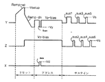
図4は、図1のようなプラズマディスプレイパネルを駆動するための従来の駆動信号を示す波形図であり、各サブフィールドSF1〜SF8でPDPの電極に供給される駆動信号を示す。 FIG. 4 is a waveform diagram showing a conventional driving signal for driving the plasma display panel as shown in FIG. 1, and shows driving signals supplied to the electrodes of the PDP in each of the subfields SF1 to SF8.
図4を参照すれば、リセット期間の初期にはすべてのスキャン電極Yに上昇ランプ信号Ramp−upが同時に供給される。これと同時に、サステイン電極Zとアドレス電極Xには0[V]が供給される。上昇ランプ信号Ramp−upによって全画面のセル内において、スキャン電極Yとアドレス電極Xとの間と、スキャン電極Yとサステイン電極Zとの間とには、弱放電で書き込み放電が起こる。この書き込み放電によってアドレス電極Xおよびサステイン電極Z上には正極性(+)の壁電荷が蓄積され、スキャン電極Y上には負極性(−)の壁電荷が蓄積される。 Referring to FIG. 4, the rising ramp signal Ramp-up is supplied to all the scan electrodes Y at the beginning of the reset period. At the same time, 0 [V] is supplied to the sustain electrode Z and the address electrode X. Due to the rising ramp signal Ramp-up, a write discharge occurs between the scan electrode Y and the address electrode X and between the scan electrode Y and the sustain electrode Z in the cells of the entire screen with a weak discharge. By this writing discharge, positive (+) wall charges are accumulated on the address electrodes X and the sustain electrodes Z, and negative (−) wall charges are accumulated on the scan electrodes Y.
このような上昇ランプ信号Ramp−upが供給された後、その上昇ランプ信号Ramp−upのピーク電圧より低いサステイン電圧Vsから落ち始めて負極性のスキャンバイアス電圧-Vyまで落ちる降下ランプ信号Ramp−dnが、スキャン電極Yに同時に供給される。これと同時に、サステイン電極Zにはサステイン電圧Vsのバイアス電圧Vz−biasが供給され、アドレス電極Xには0[V]が供給される。このように降下ランプ信号Ramp−dnが供給されるとき、スキャン電極Yとサステイン電極Zとの間と、スキャン電極Yとアドレス電極Zとの間とに、弱放電で消去放電が起こる。このような消去放電により、書き込み放電によって形成された壁電荷の中から、アドレス放電に不要な過剰壁電荷が消去される。 After the rising ramp signal Ramp-up is supplied, the falling ramp signal Ramp-dn starts to drop from the sustain voltage Vs lower than the peak voltage of the rising ramp signal Ramp-up and falls to the negative scan bias voltage -Vy. Are simultaneously supplied to the scan electrode Y. At the same time, the sustain electrode Z is supplied with the bias voltage Vz-bias of the sustain voltage Vs, and the address electrode X is supplied with 0 [V]. Thus, when the falling ramp signal Ramp-dn is supplied, an erasing discharge occurs between the scan electrode Y and the sustain electrode Z and between the scan electrode Y and the address electrode Z with a weak discharge. By such an erasing discharge, excess wall charges unnecessary for the address discharge are erased from the wall charges formed by the write discharge.
アドレス期間では、負極性スキャンパルスscanがスキャン電極Yに順次供給されると同時に、スキャンパルスscanに同期される正極性のデータパルスdataがアドレス電極Xに供給される。スキャンパルスscanとデータパルスdataとの電圧差とリセット期間に生成された壁電圧とが加えられることにより、データパルスdataが供給されるセル内ではアドレス放電が発生する。アドレス放電によって選択されたセル内には、サステイン電圧Vsが供給されるときに放電が起こりうるようにする程度の壁電荷が形成される。このアドレス期間中にサステイン電極Zには正極性直流電圧Zdcが供給される。 In the address period, the negative scan pulse scan is sequentially supplied to the scan electrode Y, and at the same time, the positive data pulse data synchronized with the scan pulse scan is supplied to the address electrode X. By adding the voltage difference between the scan pulse scan and the data pulse data and the wall voltage generated in the reset period, an address discharge is generated in the cell to which the data pulse data is supplied. In the cell selected by the address discharge, a wall charge is formed so that the discharge can occur when the sustain voltage Vs is supplied. During this address period, the positive DC voltage Zdc is supplied to the sustain electrode Z.
サステイン期間では、スキャン電極Yとサステイン電極Zに交互にサステインパルスsusが供給される。そうすると、アドレス放電によって選択された放電セル1は放電セル1内の壁電圧とサステインパルスsusとが加えられることにより、各サステインパルスsus1〜sus6が供給される度にスキャン電極Yとサステイン電極Zとの間でサステイン放電、すなわち表示放電が発生する。サステインパルスsus1〜sus6の個数は、各サブフィールドSF1〜SF8に付与された輝度加重値によってサブフィールド毎に異なるように設定される。
In the sustain period, the sustain pulse sus is alternately supplied to the scan electrode Y and the sustain electrode Z. Then, the
サステイン放電が終了した後には、図示しない消去ランプ信号がスキャン電極Yやサステイン電極Zに供給される。消去ランプ信号はセル内で弱放電で消去放電を起こすことにより、サステイン放電によって生成された壁電荷を消去させる。 After the sustain discharge is finished, an erasing ramp signal (not shown) is supplied to the scan electrode Y and the sustain electrode Z. The erasing ramp signal erases the wall charges generated by the sustain discharge by causing an erasing discharge with a weak discharge in the cell.
ところが、従来のPDPは、非表示期間に発生する光のためにコントラスト比(contrast ratio)が低いという短所がある。例えば、各サブフィールド毎に割り当てられるリセット期間中に全放電セル1内で数回発生する放電、特に上昇ランプ信号Ramp−upによって発生する書き込み放電またはセットアップ放電に伴って光が発生し、その光によってブラック輝度が高くなる。
However, the conventional PDP has a disadvantage that the contrast ratio is low due to light generated during the non-display period. For example, light is generated in association with a discharge generated several times in all
また、従来のPDPは、リセット期間が各サブフィールド毎に割り当てられるので、リセット期間の分だけのアドレス期間やサステイン期間が限定されるという問題点がある。例えば、各サブフィールド毎に割り当てられるリセット期間が原因で発生する擬似輪郭ノイズ(Contour noise)などの画質不良要因を減らすために、サブフィールドの追加や輝度の増加を必要とするが、このためのサステインパルスの追加が困難である。 Also, the conventional PDP has a problem in that the reset period is assigned to each subfield, so that the address period and the sustain period corresponding to the reset period are limited. For example, in order to reduce image quality factors such as pseudo contour noise (Contour noise) caused by the reset period assigned to each subfield, it is necessary to add subfields and increase luminance. It is difficult to add a sustain pulse.
本発明は、かかる従来の問題点を解決するためのもので、その目的は、コントラストを改善し、リセット期間を減らすようにしたPDPの初期化制御方法及び装置を提供する。 The present invention has been made to solve the above-described conventional problems, and an object thereof is to provide an initialization control method and apparatus for a PDP that improves contrast and reduces a reset period.
本発明の実施形態に係るPDPの初期化制御方法は、1フレーム期間を、入力映像の平均明るさによって初期化放電を起こすための初期化信号が省略可能であるか、前記初期化信号の電圧が調節可能である複数のサブフィールドに時分割する段階と、前記入力映像の平均明るさが以前映像の平均明るさより低い時、前記初期化信号が省略されるサブフィールドの数を増加させるか、前記初期化信号の電圧が低いサブフィールドの数を増加させる段階と、を含む。 In the initialization control method of the PDP according to the embodiment of the present invention, the initialization signal for causing the initialization discharge according to the average brightness of the input image can be omitted or the voltage of the initialization signal can be omitted for one frame period. Time-dividing into a plurality of adjustable subfields, and when the average brightness of the input video is lower than the average brightness of the previous video, increasing the number of subfields in which the initialization signal is omitted, Increasing the number of subfields having a low voltage of the initialization signal.
本発明の他の実施形態に係るPDPの初期化制御方法は、1フレーム期間を、入力映像の平均明るさによって初期化放電を起こすための初期化信号が省略可能であるか、前記初期化信号の電圧が調節可能である複数のサブフィールドに時分割する段階と、前記入力映像の平均明るさが所定の基準値であれば、前記サブフィールドのそれぞれで前記初期化信号を用いてセルの初期化を行う段階と、前記入力映像の平均明るさが前記基準値より低ければ、前記初期化信号が省略されるサブフィールドの数を増加させるか、前記初期化信号の電圧が低いサブフィールドの数を増加させる段階と、前記入力映像の平均明るさが前記基準値より高ければ、前記初期化信号が省略されるサブフィールドの数を増加させるか、前記初期化信号の電圧が低いサブフィールドの数を増加させる段階と、を含む。 In an initialization control method of a PDP according to another embodiment of the present invention, an initialization signal for causing an initialization discharge according to average brightness of an input image can be omitted in one frame period, or the initialization signal Time-division into a plurality of subfields whose voltage can be adjusted, and if the average brightness of the input video is a predetermined reference value, the initial signal of the cell using the initialization signal in each of the subfields And if the average brightness of the input video is lower than the reference value, the number of subfields in which the initialization signal is omitted is increased, or the number of subfields in which the voltage of the initialization signal is low. And if the average brightness of the input video is higher than the reference value, the number of subfields in which the initialization signal is omitted is increased or the voltage of the initialization signal is low. Comprising the steps of increasing the number of fields, the.
前記初期化信号は、電圧が徐々に上昇して弱放電で書き込み放電を起こすためのランプ信号であることを特徴とする。 The initialization signal is a ramp signal for causing an address discharge with a weak discharge by gradually increasing a voltage.
本発明の実施形態に係るPDPの初期化制御装置は、入力映像の平均明るさによって初期化放電を起こすための初期化信号が省略可能であるか、前記初期化信号の電圧が調節可能である複数のサブフィールドに時分割駆動されるPDPと、前記入力映像の平均明るさを算出するAPL算出部と、前記APL算出部によって算出された前記入力映像の平均明るさが以前映像の平均明るさより低い時、前記初期化信号が省略されるサブフィールドの数を増加させるか、前記初期化信号の電圧が低いサブフィールドの数を増加させる初期化制御部と、を備える。 In the PDP initialization control apparatus according to the embodiment of the present invention, the initialization signal for causing the initialization discharge can be omitted depending on the average brightness of the input video, or the voltage of the initialization signal can be adjusted. A PDP that is time-division driven in a plurality of subfields, an APL calculation unit that calculates the average brightness of the input video, and the average brightness of the input video calculated by the APL calculation unit is greater than the average brightness of the previous video An initialization control unit that increases the number of subfields in which the initialization signal is omitted when it is low, or increases the number of subfields in which the voltage of the initialization signal is low.
本発明の他の実施形態に係るPDPの初期化制御装置は、入力映像の平均明るさによって初期化放電を起こすための初期化信号が省略可能であるか、前記初期化信号の電圧が調節可能である複数のサブフィールドに時分割駆動されるPDPと、前記入力映像の平均明るさを算出するAPL算出部と、前記APL算出部によって算出された前記入力映像の平均明るさが所定の基準値であれば、前記サブフィールドのそれぞれで前記初期化信号を前記PDPに供給する第1初期化制御部と、前記入力映像の平均明るさが前記基準値より低ければ、前記初期化信号が省略されるサブフィールドの数を増加させるか、前記初期化信号の電圧が低いサブフィールドの数を増加させる第2初期化制御部と、前記入力映像の平均明るさが前記基準値より高ければ、前記初期化信号が省略されるサブフィールドの数を増加させるか、前記初期化信号の電圧が低いサブフィールドの数を増加させる第3初期化制御部と、を備える。 The initialization control apparatus for a PDP according to another embodiment of the present invention can omit an initialization signal for causing an initialization discharge according to an average brightness of an input image, or can adjust a voltage of the initialization signal. A PDP that is time-division driven to a plurality of subfields, an APL calculation unit that calculates the average brightness of the input video, and the average brightness of the input video calculated by the APL calculation unit is a predetermined reference value If the average brightness of the input image is lower than the reference value, the initialization signal is omitted if the first initialization control unit supplies the initialization signal to the PDP in each of the subfields. A second initialization control unit for increasing the number of subfields to be increased or increasing the number of subfields for which the voltage of the initialization signal is low, and the average brightness of the input video is higher than the reference value. If provided or to increase the number of subfields where the initialization signal is omitted, and the third initialization control unit to increase the number of subfields voltage is low the initialization signal.
前記初期化信号は、電圧が徐々に上昇して弱放電で書き込み放電を起こすためのランプ信号である。 The initialization signal is a ramp signal for causing an address discharge with a weak discharge by gradually increasing the voltage.
前記初期化制御部は、前記初期化信号を発生させる初期化信号発生部と、前記APLによって算出された平均明るさ信号に応答して前記初期化信号発生部を制御するための制御部と、を備える。 The initialization control unit includes: an initialization signal generation unit that generates the initialization signal; a control unit that controls the initialization signal generation unit in response to an average brightness signal calculated by the APL; Is provided.
本発明に係るPDPの初期化制御方法及び装置は、APLが基準値より低い時及び/または高い時、上昇ランプ信号を省略するか、そのセットアップ電圧を低下させる。その結果、本発明は、初期化放電数を減らすか初期化放電を弱くして、放電時に伴う光放出量を減らすことにより、ブラック輝度を低めてコントラスト比を向上させ且つリセット期間を減らすことができる。 The PDP initialization control method and apparatus according to the present invention omits the rising ramp signal or lowers its setup voltage when the APL is lower and / or higher than the reference value. As a result, the present invention can reduce the black luminance, improve the contrast ratio, and reduce the reset period by reducing the number of initializing discharges or weakening the initializing discharges, thereby reducing the amount of light emission accompanying the discharge. it can.
以下、本発明の実施形態を添付図を参照して詳しく説明する。 Hereinafter, embodiments of the present invention will be described in detail with reference to the accompanying drawings.
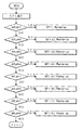
(1)第1実施形態
図5は、本発明の第1実施形態に係るプラズマディスプレイパネルの初期化制御方法の制御手順を段階的に示す流れ図である。
(1) 1st Embodiment FIG. 5: is a flowchart which shows the control procedure of the initialization control method of the plasma display panel based on 1st Embodiment of this invention in steps.
本発明の第1実施形態に係るPDPの初期化制御方法は、1画面の平均輝度レベル(Average Picture Level:以下、「APL」という)を算出し、そのAPLが低いほど高い加重値のサブフィールドにおいて上昇ランプ信号Ramp−upをより多く省略する。 The PDP initialization control method according to the first embodiment of the present invention calculates an average picture level (hereinafter referred to as “APL”) of one screen, and the lower the APL, the higher the weighted subfield. In FIG. 5, the rising ramp signal Ramp-up is omitted more.
次の表1と図5は、サブフィールド8個で最大1024階調まで表現できるサブフィールドパターンを仮定し、本発明の第1実施形態に係るPDPの初期化制御方法において上昇ランプ信号Ramp−upの省略可否を示す。 Table 1 and FIG. 5 assume a subfield pattern that can represent a maximum of 1024 gradations with 8 subfields, and the rising ramp signal Ramp-up in the initialization control method of the PDP according to the first embodiment of the present invention. Indicates whether or not can be omitted.

表1において、かっこの中の数字は各サブフィールドに付与される輝度加重値であり‘k’はAPLによって輝度加重値を最大4倍に乗算させる値である。例えば、APLが低いほど第8サブフィールドSF8の加重値‘128'は‘256'、‘384'、‘512'に調整される。 In Table 1, the numbers in parentheses are the luminance weight values assigned to each subfield, and 'k' is a value for multiplying the luminance weight values by a maximum of four times by APL. For example, as the APL is lower, the weight value '128' of the eighth subfield SF8 is adjusted to '256', '384', and '512'.
APLは最大1024の階調に対応して0〜1023まで総1024段階に細分化され、総1024段階のAPLは表1のようにさらに8個のAPL群に分けられる。第1APL群APL1は最も低い範囲のAPLであって0〜100段階のAPLを含み、第2APL群APL2は101〜200段階のAPLを含む。第3APL群APL3は201〜300段階のAPL、第4APL群APL4は301〜400段階のAPL、第5APL群APL5は401〜500段階のAPL、第6APL群APL6は501〜600段階のAPL、第7APL群APL7は601〜700段階のAPLをそれぞれ含む。また、第8APL群APL8は最も高い範囲のAPLであって701〜1023段階のAPLを含む。 APL is subdivided into a total of 1024 stages from 0 to 1023 corresponding to a maximum of 1024 gradations, and the APL of 1024 stages is further divided into 8 APL groups as shown in Table 1. The first APL group APL1 is the lowest APL and includes 0 to 100 stages of APL, and the second APL group APL2 includes 101 to 200 stages of APL. The third APL group APL3 is 201-300 stage APL, the fourth APL group APL4 is 301-400 stage APL, the fifth APL group APL5 is 401-500 stage APL, the sixth APL group APL6 is 501-600 stage APL, the seventh APL Group APL7 includes 601-700 stages of APL, respectively. Further, the eighth APL group APL8 is the highest APL and includes 701 to 1023 stages of APL.
表1及び図5に示すように、APLが第1APL群APL1に算出されると、輝度加重値が最も低い第1サブフィールドSF1にのみ上昇ランプ信号Ramp−upが割り当てられ、その以外のサブフィールドSF2〜SF8には上昇ランプ信号Ramp−upが割り当てられない。 As shown in Table 1 and FIG. 5, when the APL is calculated for the first APL group APL1, the rising ramp signal Ramp-up is assigned only to the first subfield SF1 having the lowest luminance weight, and the other subfields The rising ramp signal Ramp-up is not assigned to SF2 to SF8.
また、APLが101〜200間の値、すなわち第2APL群APL2に算出されると、第1及び第2サブフィールドSF1、SF2にのみ上昇ランプ信号Ramp−upが印加される。 When the APL is calculated to a value between 101 and 200, that is, the second APL group APL2, the rising ramp signal Ramp-up is applied only to the first and second subfields SF1 and SF2.
画面が明るくなるとともにAPLが601〜700間の値、すなわち第7APL群APL7に算出されると、第8サブフィールドSF8を除いた第1〜第7サブフィールドSF1〜SF7に上昇ランプ信号Ramp−upが印加され、画面がピークホワイトに近づく明るさにさらに明るくなるとともにAPLが701〜1023間の値、すなわち第8APL群APL8に算出されると、すべてのサブフィールドSF1〜SF8に上昇ランプ信号Ramp−upが印加される。 When the screen becomes brighter and the APL is calculated to a value between 601 and 700, that is, the seventh APL group APL7, the rising ramp signal Ramp-up is displayed in the first to seventh subfields SF1 to SF7 excluding the eighth subfield SF8. Is applied, and the brightness of the screen approaches peak white and the APL is calculated to a value between 701 and 1023, that is, the eighth APL group APL8, the rising ramp signal Ramp− is applied to all subfields SF1 to SF8. up is applied.
APL値が低ければ、すなわち画面が比較的暗い場合にはデータが最下位ビット(Least Significant Bits:LSB)に対応する低輝度加重値のサブフィールド、例えば第1〜第3サブフィールドSF1〜SF3に主に存在する一方、最上位ビット(Most Significant Bits:MSB)に対応する高輝度加重値のサブフィールドにはほとんど存在しない。 If the APL value is low, that is, if the screen is relatively dark, the data is stored in a subfield of a low luminance weight value corresponding to the least significant bit (Least Significant Bits: LSB), for example, the first to third subfields SF1 to SF3. While it exists mainly, it hardly exists in the subfield of the high-intensity weight value corresponding to the most significant bit (Most Significant Bits: MSB).
よって、本発明の第1実施形態に係るPDPの初期化制御方法は、暗い画面でデータが存在するサブフィールドの初期化を安定化させる一方、データのない、すなわち点灯するセルがほとんどない高輝度加重値のサブフィールドでリセット期間を減らすか省略することにより、暗い画面でブラック輝度を低めてコントラスト比を高める。また、本発明の第1実施形態に係るPDPの初期化制御方法は、明るい画面でリセット期間が含まれるサブフィールドの個数を増加させ、データが存在可能なほぼすべてのサブフィールドの初期化を安定化させることで、各サブフィールド毎の駆動マージンを充分に確保することができる。 Therefore, the initialization control method of the PDP according to the first embodiment of the present invention stabilizes the initialization of a subfield where data exists on a dark screen, while having no data, that is, high brightness with few cells to be lit. By reducing or omitting the reset period in the weighted subfield, the black luminance is lowered and the contrast ratio is increased in a dark screen. In addition, the initialization control method of the PDP according to the first embodiment of the present invention increases the number of subfields including a reset period on a bright screen, and stabilizes initialization of almost all subfields where data can exist. As a result, a sufficient driving margin for each subfield can be secured.
一方、降下ランプ信号Ramp−dnは各サブフィールド毎に割り当てることもでき、APLによって上昇ランプ信号Ramp−upと同様に省略することもできる。 On the other hand, the falling ramp signal Ramp-dn can be assigned to each subfield, and can be omitted by the APL in the same manner as the rising ramp signal Ramp-up.
本発明の第2実施形態に係るPDPの初期化制御方法は、1画面のAPLを算出し、そのAPLが低いほど高い加重値のサブフィールドにおいて上昇ランプ信号Ramp−upをより多く省略するとともに、APLが高いほど低い加重値のサブフィールドにおいて上昇ランプ信号Ramp−upをより多く省略する。 In the PDP initialization control method according to the second embodiment of the present invention, the APL of one screen is calculated, and the lower the APL, the more the rising ramp signal Ramp-up is omitted in the higher weight subfield, The higher the APL is, the more the ramp-up signal Ramp-up is omitted in the sub-field with a lower weight value.
(2)第2実施形態
図6は、本発明の第2実施形態に係るプラズマディスプレイパネルの初期化制御方法の制御手順を段階的に示す流れ図である。次の表2と図6は、サブフィールド8個で最大1024階調まで表現できるサブフィールドパターンを仮定し、本発明の第2実施形態に係るPDPの初期化制御方法において上昇ランプ信号Ramp−upの省略可否を示す。
(2) Second Embodiment FIG. 6 is a flowchart showing step-by-step a control procedure of a plasma display panel initialization control method according to a second embodiment of the present invention. The following Table 2 and FIG. 6 assume a subfield pattern that can represent up to 1024 gradations with 8 subfields, and the rising ramp signal Ramp-up in the initialization control method of the PDP according to the second embodiment of the present invention. Indicates whether or not can be omitted.
表2及び図6に示すように、APLが第1APL群APL1に算出されると、輝度加重値が最も低い第1及び第2サブフィールドSF1、SF2にのみ上昇ランプ信号Ramp−upが割り当てられ、その以外のサブフィールドSF3〜SF8には上昇ランプ信号Ramp−upが割り当てられない。また、APLが101〜200間の値、すなわち第2APL群APL2に算出されると、第1〜第4サブフィールドSF1〜SF4に上昇ランプ信号Ramp−upが印加され、APLが第3APL群APL3に算出されると、第1〜第6サブフィールドSF1〜SF6に上昇ランプ信号Ramp−upが印加される。 As shown in Table 2 and FIG. 6, when the APL is calculated for the first APL group APL1, the rising ramp signal Ramp-up is assigned only to the first and second subfields SF1 and SF2 having the lowest luminance weight values. The ramp-up signal Ramp-up is not assigned to the other subfields SF3 to SF8. Further, when the APL is calculated to a value between 101 and 200, that is, the second APL group APL2, the rising ramp signal Ramp-up is applied to the first to fourth subfields SF1 to SF4, and the APL is applied to the third APL group APL3. When calculated, the rising ramp signal Ramp-up is applied to the first to sixth subfields SF1 to SF6.
画面が中間の明るさになるとともにAPLが第4及び第5APL群APL4、APL5中に算出されると、上昇ランプ信号Ramp−upはすべてのサブフィールドSF1〜SF8に印加される。 When the screen has an intermediate brightness and APL is calculated in the fourth and fifth APL groups APL4 and APL5, the rising ramp signal Ramp-up is applied to all the subfields SF1 to SF8.
画面がさらに明るくなるとともにAPLが第6APL群APL6に算出されると、第3〜第8サブフィールドSF3〜SF8に上昇ランプ信号Ramp−upが印加され、第7APL群APL7に算出されると、第5〜第8サブフィールドSF5〜SF8に上昇ランプ信号Ramp−upが印加される。画面がピークホワイトに近づきさらに明るくなるとともにAPLが第8APL群APL8に算出されると、第7及び第8サブフィールドSF7、SF8にのみ上昇ランプ信号Ramp−upが印加される。 When the screen becomes brighter and APL is calculated for the sixth APL group APL6, the rising ramp signal Ramp-up is applied to the third to eighth subfields SF3 to SF8, and when the APL is calculated for the seventh APL group APL7, The rising ramp signal Ramp-up is applied to the fifth to eighth subfields SF5 to SF8. When the screen approaches peak white and becomes brighter and APL is calculated for the eighth APL group APL8, the rising ramp signal Ramp-up is applied only to the seventh and eighth subfields SF7 and SF8.
APL値が低ければ、すなわち画面が比較的暗い場合には最下位ビット(Least Significant Bits:LSB)側に対応する低輝度加重値のサブフィールド、例えば第1〜第3サブフィールドSF1〜SF3にデータが主に存在する一方、最上位ビット(Most Significant Bits:MSB)側に対応する高輝度加重値のサブフィールドにデータがほとんど存在しない。そして、放電回数が多いほど放電セル内に荷電粒子が多くなり、安定化したプライミング效果が強まり、放電セルの放電特性が安定化される。 If the APL value is low, that is, if the screen is relatively dark, data is stored in a subfield of a low luminance weight value corresponding to the least significant bit (LSB) side, for example, first to third subfields SF1 to SF3. However, there is almost no data in the subfield of the high luminance weight value corresponding to the most significant bit (MSB) side. As the number of discharges increases, the number of charged particles in the discharge cell increases, and the stabilized priming effect increases, and the discharge characteristics of the discharge cell are stabilized.
よって、本発明の第2実施形態に係るPDPの初期化制御方法は、暗い画面でデータが存在するサブフィールドの初期化を安定化させる一方、データがない、すなわち点灯するセルがほとんどない高輝度加重値のサブフィールドでリセット期間を省略することにより、暗い画面でブラック輝度を低めてコントラスト比を高める。 Therefore, the initialization control method of the PDP according to the second embodiment of the present invention stabilizes the initialization of a subfield where data exists on a dark screen, while having no data, that is, high brightness with few cells to be lit. By omitting the reset period in the weighted subfield, the black luminance is lowered and the contrast ratio is increased in a dark screen.
本発明の第2実施形態に係るPDPの初期化制御方法は、放電回数が多くなるため、比較的各サブフィールドで駆動マージンが高くなる明るい画面において、明るさが明るくなるほど上昇ランプ信号Ramp−upが省略されるサブフィールドの個数を増加させる。明るい画面で上昇ランプ信号Ramp−upが省略されるサブフィールドは、明るい画面で最上位ビットMSB側にデータの存在する確率が高いため、最下位ビットMSBに側に対応する低輝度加重値のサブフィールドでリセット期間が省略される。 In the PDP initialization control method according to the second embodiment of the present invention, since the number of discharges increases, the rising ramp signal Ramp-up increases as the brightness increases on a bright screen where the drive margin is relatively high in each subfield. Increase the number of subfields where is omitted. The subfield in which the rising ramp signal Ramp-up is omitted on a bright screen has a high probability that data exists on the most significant bit MSB side on a bright screen, and therefore, the sub-field of the low luminance weight value corresponding to the least significant bit MSB side. The reset period is omitted in the field.
図7は、本発明の第1及び第2実施形態に係るPDPの初期化制御方法において上昇ランプ信号Ramp−upが省略されるサブフィールドの駆動信号を示す。図7に示すように、本発明の第1及び第2実施形態に係るPDPの初期化制御方法は、確率的にデータがほとんどないサブフィールドで上昇ランプ信号Ramp−upが省略されるので、その分リセット期間が短くなり、リセット期間で書き込み放電が発生しないので、ブラック輝度が低くなる。 FIG. 7 illustrates a driving signal of a subfield in which the rising ramp signal Ramp-up is omitted in the PDP initialization control method according to the first and second embodiments of the present invention. As shown in FIG. 7, in the PDP initialization control method according to the first and second embodiments of the present invention, the rising ramp signal Ramp-up is omitted in a subfield where there is almost no data in probability. Since the minute reset period is shortened and no writing discharge is generated in the reset period, the black luminance is lowered.
(3)第3実施形態
本発明の第3実施形態に係るPDPの初期化制御方法は、APLが低いほど、第1サブフィールドSF1を除いた残りのサブフィールドSF2〜SF8で上昇ランプ信号Ramp−upのセットアップ電圧Vsetupを低下させる。
(3) Third Embodiment In the PDP initialization control method according to the third embodiment of the present invention, the lower the APL, the higher the ramp signal Ramp− in the remaining subfields SF2 to SF8 excluding the first subfield SF1. The setup voltage Vsetup of up is lowered.
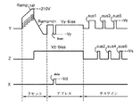
図8は、本発明の第3実施形態に係るプラズマディスプレイパネルの初期化制御方法の制御手順を段階的に示す流れ図である。次の表3と図8は、サブフィールド8個で最大1024階調まで表現できるサブフィールドパターンを仮定し、本発明の第3実施形態に係るPDPの初期化制御方法において上昇ランプ信号Ramp−upのセットアップ電圧Vsetupを示す。 FIG. 8 is a flowchart showing step by step the control procedure of the plasma display panel initialization control method according to the third embodiment of the present invention. Table 3 and FIG. 8 assume a subfield pattern that can represent up to 1024 gray levels with 8 subfields, and the rising ramp signal Ramp-up in the initialization control method of the PDP according to the third embodiment of the present invention. The setup voltage Vsetup is shown.
第1サブフィールドSF1はフレームがスタートするサブフィールドであって初期化を最も安定化させる必要がある。このために第1サブフィールドSF1では、APLにかかわらず180V〜240V間の電圧、好ましくは210Vセットアップ電圧の上昇ランプ信号Ramp−upで初期化のための書き込み放電を発生させる。この第1サブフィールドSF1を除いた他のサブフィールドSF2〜SF8では、APLによって上昇ランプ信号Ramp−upのセットアップ電圧Vsetupが変わる。APLが低い時、すなわち暗い画面でブラック輝度が低くなるほどAPLが低い値に算出され、第2〜第8サブフィールドSF2〜SF8におけるセットアップ電圧Vsetupは低くなる。 The first subfield SF1 is a subfield where a frame starts, and initialization needs to be most stabilized. For this reason, in the first subfield SF1, a write discharge for initialization is generated with a rising ramp signal Ramp-up having a voltage between 180V and 240V, preferably a 210V setup voltage, regardless of APL. In the other subfields SF2 to SF8 excluding the first subfield SF1, the setup voltage Vsetup of the rising ramp signal Ramp-up is changed by APL. When the APL is low, that is, the black luminance is lowered on a dark screen, the APL is calculated to be a lower value, and the setup voltage Vsetup in the second to eighth subfields SF2 to SF8 is lowered.
表3と図8に示すように、APLが第1APL群APL1に算出されると、第2〜第8サブフィールドSF2〜SF8におけるセットアップ電圧Vsetupは、100Vというふうに最も低く設定される。APLが第2APL群APL2に算出されると、第2〜第8サブフィールドSF2〜SF8におけるセットアップ電圧Vsetupは110Vに設定される。 As shown in Table 3 and FIG. 8, when the APL is calculated for the first APL group APL1, the setup voltage Vsetup in the second to eighth subfields SF2 to SF8 is set to the lowest value of 100V. When the APL is calculated for the second APL group APL2, the setup voltage Vsetup in the second to eighth subfields SF2 to SF8 is set to 110V.
このようにAPLが高いほどセットアップ電圧Vsetupは高く設定され、画面が明るくなるとともにAPLが第7APL群APL7に算出されると、第2〜第8サブフィールドSF2〜SF8におけるセットアップ電圧Vsetupは160Vに設定され、第8APL群APL8に算出されると、第2〜第8サブフィールドSF2〜SF8におけるセットアップ電圧Vsetupは170Vに設定される。 Thus, the higher the APL, the higher the setup voltage Vsetup is set, the brighter the screen is, and when the APL is calculated for the seventh APL group APL7, the setup voltage Vsetup in the second to eighth subfields SF2 to SF8 is set to 160V. When calculated for the eighth APL group APL8, the setup voltage Vsetup in the second to eighth subfields SF2 to SF8 is set to 170V.
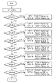
(4)第4実施形態
本発明の第4実施形態に係るPDPの初期化制御方法は、APLが低いほど又はAPLが高いほど、第1サブフィールドSF1を除いた残りのサブフィールドSF2〜SF8における上昇ランプ信号Ramp−upのセットアップ電圧Vsetupが低くなる。
(4) Fourth Embodiment In the PDP initialization control method according to the fourth embodiment of the present invention, the lower the APL or the higher the APL, the remaining subfields SF2 to SF8 excluding the first subfield SF1. The setup voltage Vsetup of the rising ramp signal Ramp-up is lowered.
図9は、本発明の第4実施形態に係るプラズマディスプレイパネルの初期化制御方法の制御手順を段階的に示す流れ図である。次の表4と図9は、サブフィールド8個で最大1024階調まで表現できるサブフィールドパターンを仮定し、本発明の第4実施形態に係るPDPの初期化制御方法において上昇ランプ信号Ramp−upのセットアップ電圧Vsetupを示す。 FIG. 9 is a flowchart showing step by step the control procedure of the plasma display panel initialization control method according to the fourth embodiment of the present invention. Table 4 and FIG. 9 assume a subfield pattern that can represent a maximum of 1024 gradations with 8 subfields, and the rising ramp signal Ramp-up in the initialization control method of the PDP according to the fourth embodiment of the present invention. The setup voltage Vsetup is shown.
第1サブフィールドSF1はフレームがスタートするサブフィールドであって初期化を最も安定化させる必要がある。このために第1サブフィールドSF1では、APLにかかわらず180V〜240V間の電圧、好ましくは210Vセットアップ電圧の上昇ランプ信号Ramp−upで初期化のための書き込み放電を発生させる。この第1サブフィールドSF1を除いた他のサブフィールドSF2〜SF8では、APLによって上昇ランプ信号Ramp−upのセットアップ電圧Vsetupが変わる。 The first subfield SF1 is a subfield where a frame starts, and initialization needs to be most stabilized. For this reason, in the first subfield SF1, a write discharge for initialization is generated with a rising ramp signal Ramp-up having a voltage between 180V and 240V, preferably a 210V setup voltage, regardless of APL. In the other subfields SF2 to SF8 excluding the first subfield SF1, the setup voltage Vsetup of the rising ramp signal Ramp-up is changed by APL.
APLが低い時、すなわち暗い画面でブラック輝度の低くなるほどAPLが低い値に算出され、第2〜第8サブフィールドSF2〜SF8におけるセットアップ電圧Vsetupは低くなる。APLが高い時、すなわち明るい画面では放電回数が多いためプライミング效果が強い。このために、明るい画面ではセットアップ電圧Vsetupが低い場合にも初期化のための書き込み放電を全放電セルで安定して起こすことができるので、APLが高い値に算出されると、第2〜第8サブフィールドSF2〜SF8におけるセットアップ電圧Vsetupは低くなる。 When the APL is low, that is, the black luminance is lowered on a dark screen, the APL is calculated to be a lower value, and the setup voltage Vsetup in the second to eighth subfields SF2 to SF8 is lowered. When the APL is high, that is, a bright screen, the number of discharges is large, so the priming effect is strong. For this reason, in a bright screen, even when the setup voltage Vsetup is low, the write discharge for initialization can be stably caused in all the discharge cells. Therefore, when the APL is calculated to be a high value, The setup voltage Vsetup in the 8 subfields SF2 to SF8 is lowered.
表4と図9に示すように、APLが第1APL群APL1に算出されると、第2〜第8サブフィールドSF2〜SF8におけるセットアップ電圧Vsetupは、100Vに最も低く設定される。APLが第2APL群APL2に算出されると、第2〜第8サブフィールドSF2〜SF8におけるセットアップ電圧Vsetupは110Vに設定される。このようにAPLが高いほどセットアップ電圧Vsetupは高く設定されるが、画面が明るくなるとともにAPLが第6APL群APL6に算出されると、第2〜第8サブフィールドSF2〜SF8におけるセットアップ電圧Vsetupは130Vとまた低く設定される。また、さらに画面が明るくなるとどセットアップ電圧Vsetupは徐々に低く設定される。すなわち、APLが第7APL群APL7に算出されると、第2〜第8サブフィールドSF2〜SF8におけるセットアップ電圧Vsetupは120Vに設定され、第8APL群APL8に算出されると、第2〜第8サブフィールドSF2〜SF8におけるセットアップ電圧Vsetupは110Vに設定される。 As shown in Table 4 and FIG. 9, when the APL is calculated for the first APL group APL1, the setup voltage Vsetup in the second to eighth subfields SF2 to SF8 is set to the lowest value of 100V. When the APL is calculated for the second APL group APL2, the setup voltage Vsetup in the second to eighth subfields SF2 to SF8 is set to 110V. Thus, the higher the APL, the higher the setup voltage Vsetup is set. However, when the screen becomes brighter and the APL is calculated for the sixth APL group APL6, the setup voltage Vsetup in the second to eighth subfields SF2 to SF8 is 130V. And set too low. Further, as the screen becomes brighter, the setup voltage Vsetup is gradually set lower. That is, when APL is calculated for the seventh APL group APL7, the setup voltage Vsetup in the second to eighth subfields SF2 to SF8 is set to 120V, and when calculated for the eighth APL group APL8, the second to eighth subfields are calculated. The setup voltage Vsetup in the fields SF2 to SF8 is set to 110V.
図10は、本発明の第3及び第4実施形態に係るプラズマディスプレイパネルの初期化制御方法において上昇ランプ波形Ramp−upのセットアップ電圧Vsetupが平均明るさによって変わることを示す波形図である。図10は、本発明の第3及び第4実施形態に係るPDPの初期化制御方法において上昇ランプ信号Ramp−upのセットアップ電圧Vsetupを示す。 FIG. 10 is a waveform diagram showing that the setup voltage Vsetup of the rising ramp waveform Ramp-up varies depending on the average brightness in the plasma display panel initialization control method according to the third and fourth embodiments of the present invention. FIG. 10 shows the setup voltage Vsetup of the rising ramp signal Ramp-up in the PDP initialization control method according to the third and fourth embodiments of the present invention.
図10に示すように、本発明の第3及び第4実施形態に係るPDPの初期化制御方法は、APLによって少なくとも一部サブフィールドで上昇ランプ信号Ramp−upのセットアップ電圧Vsetupが点線で示すように100V〜200V間で可変的に設定される。セットアップ電圧Vsetupが点線のように低く設定されると、その分上昇ランプ信号Ramp−upによる書き込み放電が弱く発生してブラック輝度を低めることができる。 As shown in FIG. 10, in the PDP initialization control method according to the third and fourth embodiments of the present invention, the setup voltage Vsetup of the rising ramp signal Ramp-up is indicated by a dotted line in at least a partial subfield by APL. Is variably set between 100V and 200V. When the setup voltage Vsetup is set low as shown by the dotted line, the write discharge due to the rising ramp signal Ramp-up is weakly generated and the black luminance can be lowered.
(5)第5実施形態
本発明の第5実施形態に係るPDPの初期化制御方法は、APLが低いほど、上昇ランプ信号Ramp−upが省略されるサブフィールドの個数を多くするか、少なくとも一部サブフィールドで上昇ランプ信号Ramp−upのセットアップ電圧Vsetupを低く設定する。また、本発明の第5実施形態に係るPDPの初期化制御方法は、APLが高いほど、上昇ランプ信号Ramp−upが省略されるサブフィールドの個数を少なくするか、少なくとも一部サブフィールドで上昇ランプ信号Ramp−upのセットアップ電圧Vsetupを高く設定する。
(5) Fifth Embodiment The PDP initialization control method according to the fifth embodiment of the present invention increases the number of subfields in which the rising ramp signal Ramp-up is omitted as the APL is lower, or at least one. The set-up voltage Vsetup of the rising ramp signal Ramp-up is set low in the sub-field. In addition, in the PDP initialization control method according to the fifth embodiment of the present invention, the higher the APL, the smaller the number of subfields in which the rising ramp signal Ramp-up is omitted or the increase in at least some subfields. The setup voltage Vsetup of the ramp signal Ramp-up is set high.
次の表5と図11は、サブフィールド8個で最大1024階調まで表現できるサブフィールドパターンを仮定し、本発明の第5実施形態に係るPDPの初期化制御方法において上昇ランプ信号Ramp−upの省略可否とセットアップ電圧Vsetupを示す。 Table 5 and FIG. 11 assume a subfield pattern that can represent a maximum of 1024 gradations with 8 subfields, and the rising ramp signal Ramp-up in the PDP initialization control method according to the fifth embodiment of the present invention. The setup voltage Vsetup is shown.
表5において、‘あり'は上昇ランプ信号Ramp−upが省略されないサブフィールド、即ち上昇ランプ信号Ramp−upありを意味する。このサブフィールドでは正常な210Vセットアップ電圧Vsetupの上昇ランプ信号Ramp−upが印加される。‘なし'は上昇ランプ信号Ramp−upが省略されるか、セットアップ電圧Vsetupが140Vに低く設定される上昇ランプ信号Ramp−upが印加されるサブフィールドを意味する。 In Table 5, 'Yes' means a subfield in which the rising ramp signal Ramp-up is not omitted, that is, the rising ramp signal Ramp-up is present. In this subfield, a rising ramp signal Ramp-up having a normal 210V setup voltage Vsetup is applied. 'None' means a sub-field to which the rising ramp signal Ramp-up is omitted or the rising ramp signal Ramp-up in which the setup voltage Vsetup is set low to 140V is applied.
第1サブフィールドSF1では210Vセットアップ電圧の上昇ランプ信号Ramp−upで初期化のための書き込み放電が発生する。この第1サブフィールドSF1を除いた他のサブフィールドSF2〜SF8では、APLによって上昇ランプ信号Ramp−upが省略されるか、上昇ランプ信号Ramp−upのセットアップ電圧Vsetupが変わる。APLが低い時、すなわち暗い画面でブラック輝度の低くなるようにAPLが低い値に算出されると、第2〜第8サブフィールドSF2〜SF8の少なくとも一部には上昇ランプ信号Ramp−upが省略されるか、低いセットアップ電圧Vsetupの上昇ランプ信号Ramp−upが印加される。 In the first subfield SF1, a write discharge for initialization is generated by the rising ramp signal Ramp-up having a setup voltage of 210V. In the other subfields SF2 to SF8 excluding the first subfield SF1, the rising ramp signal Ramp-up is omitted or the setup voltage Vsetup of the rising ramp signal Ramp-up is changed by APL. When the APL is low, that is, when the APL is calculated to be low so that the black luminance is low on a dark screen, the rising ramp signal Ramp-up is omitted in at least a part of the second to eighth subfields SF2 to SF8. Or a ramp-up signal Ramp-up with a low setup voltage Vsetup is applied.
表5と図11に示すように、APLが第1APL群APL1に算出されると、第2〜第8サブフィールドSF2〜SF8には100Vのセットアップ電圧Vsetupの上昇ランプ信号Ramp−upが印加される。APLが第2APL群APL2に算出されると、第2〜第8サブフィールドSF2〜SF8には120Vのセットアップ電圧Vsetupの上昇ランプ信号Ramp−upが印加される。APLが第3APL群APL3に算出されると、第2〜第8サブフィールドSF2〜SF8には上昇ランプ信号Ramp−upが省略されるか、140Vのセットアップ電圧Vsetupの上昇ランプ信号Ramp−upが印加される。APLが第4APL群APL4に算出されると、第1及び第2サブフィールドSF1、SF2には210Vのセットアップ電圧Vsetupの上昇ランプ信号Ramp−upが印加され、第3〜第8サブフィールドSF3〜SF8には上昇ランプ信号Ramp−upが省略されるか、140Vのセットアップ電圧Vsetupの上昇ランプ信号Ramp−upが印加される。APLが第5APL群APL5に算出されると、第1〜第3サブフィールドSF1〜SF3には210Vのセットアップ電圧Vsetupの上昇ランプ信号Ramp−upが印加され、第4〜第8サブフィールドSF4〜SF8には上昇ランプ信号Ramp−upが省略されるか、140Vのセットアップ電圧Vsetupの上昇ランプ信号Ramp−upが印加される。 As shown in Table 5 and FIG. 11, when the APL is calculated for the first APL group APL1, the ramp-up signal Ramp-up of the setup voltage Vsetup of 100V is applied to the second to eighth subfields SF2 to SF8. . When the APL is calculated for the second APL group APL2, the rising ramp signal Ramp-up having the setup voltage Vsetup of 120V is applied to the second to eighth subfields SF2 to SF8. When APL is calculated for the third APL group APL3, the rising ramp signal Ramp-up is omitted or the rising ramp signal Ramp-up of the 140V setup voltage Vsetup is applied to the second to eighth subfields SF2 to SF8. Is done. When the APL is calculated for the fourth APL group APL4, the rising ramp signal Ramp-up of the setup voltage Vsetup of 210V is applied to the first and second subfields SF1 and SF2, and the third to eighth subfields SF3 to SF8 are applied. The rising ramp signal Ramp-up is omitted, or the rising ramp signal Ramp-up having a setup voltage Vsetup of 140V is applied. When APL is calculated for the fifth APL group APL5, the rising ramp signal Ramp-up of the setup voltage Vsetup of 210 V is applied to the first to third subfields SF1 to SF3, and the fourth to eighth subfields SF4 to SF8. The rising ramp signal Ramp-up is omitted, or the rising ramp signal Ramp-up having a setup voltage Vsetup of 140V is applied.
このように、APLが高いほど、上昇ランプ信号Ramp−upが省略されるサブフィールドの個数が減るか、低いセットアップ電圧Vsetupの上昇ランプ信号Ramp−upが印加されるサブフィールドの個数が減る。すなわち、画面が明るくなるとともにAPLが第7APL群APL7に算出されると、第1〜第5サブフィールドSF1〜SF5には210Vのセットアップ電圧Vsetupの上昇ランプ信号Ramp−upが印加され、第6〜第8サブフィールドSF6〜SF8には上昇ランプ信号Ramp−upが省略されるか、140Vのセットアップ電圧Vsetupの上昇ランプ信号Ramp−upが印加される。また、APLが第8APL群APL8に算出されると、第1〜第6サブフィールドSF1〜SF6には210Vのセットアップ電圧Vsetupの上昇ランプ信号Ramp−upが印加され、第7及び第8サブフィールドSF7、SF8には上昇ランプ信号Ramp−upが省略されるか、140Vのセットアップ電圧Vsetupの上昇ランプ信号Ramp−upが印加される。 Thus, the higher the APL, the smaller the number of subfields in which the rising ramp signal Ramp-up is omitted or the number of subfields to which the rising ramp signal Ramp-up of the low setup voltage Vsetup is applied. That is, when the screen is brightened and APL is calculated for the seventh APL group APL7, the rising ramp signal Ramp-up of the setup voltage Vsetup of 210V is applied to the first to fifth subfields SF1 to SF5, and the sixth to fifth subfields SF1 to SF5 are applied. In the eighth subfields SF6 to SF8, the rising ramp signal Ramp-up is omitted or the rising ramp signal Ramp-up having the setup voltage Vsetup of 140V is applied. When the APL is calculated for the eighth APL group APL8, the ramp-up signal Ramp-up of the setup voltage Vsetup of 210V is applied to the first to sixth subfields SF1 to SF6, and the seventh and eighth subfields SF7. , SF8, the ramp-up signal Ramp-up is omitted, or the ramp-up signal Ramp-up having the setup voltage Vsetup of 140V is applied.
本発明の第5実施形態に係るPDPの初期化制御方法の他の例は、表6のようにAPLが低いほど、上昇ランプ信号Ramp−upが省略されるサブフィールドの個数を多くし、APLが高い時、少なくとも一部サブフィールドで上昇ランプ信号Ramp−upのセットアップ電圧Vsetupが低く設定される。 In another example of the initialization control method of the PDP according to the fifth embodiment of the present invention, as the APL is lower as shown in Table 6, the number of subfields in which the rising ramp signal Ramp-up is omitted is increased. Is high, the setup voltage Vsetup of the rising ramp signal Ramp-up is set low in at least some subfields.
(6)第6実施形態
本発明の第6実施形態に係るPDPの初期化制御方法は、APLが低いほど又はAPLが高いほど、上昇ランプ信号Ramp−upが省略されるか、上昇ランプ信号Ramp−upのセットアップ電圧Vsetupが低く設定される。
(6) Sixth Embodiment In the initialization control method for a PDP according to the sixth embodiment of the present invention, the lower the APL or the higher the APL, the more the rising ramp signal Ramp-up is omitted or the rising ramp signal Ramp. -The setup voltage Vsetup of -up is set low.
次の表7と図12は、サブフィールド8個で最大1024階調まで表現できるサブフィールドパターンを仮定し、本発明の第6実施形態に係るPDPの初期化制御方法において上昇ランプ信号Ramp−upの省略可否とセットアップ電圧Vsetupを示す。 The following Table 7 and FIG. 12 assume a subfield pattern that can represent up to 1024 gradations with 8 subfields, and the rising ramp signal Ramp-up in the initialization control method of the PDP according to the sixth embodiment of the present invention. The setup voltage Vsetup is shown.
第1サブフィールドSF1はフレームがスタートするサブフィールドであって初期化を最も安定化させる必要がある。このために第1サブフィールドSF1では、APLにかかわらず180V〜240V間の電圧、好ましくは210Vセットアップ電圧の上昇ランプ信号Ramp−upで初期化のための書き込み放電を発生させる。この第1サブフィールドSF1を除いた他のサブフィールドSF2〜SF8では、APLが低い時とAPLが高い時、上昇ランプ信号Ramp−upが省略されるサブフィールドの個数が増加するか、セットアップ電圧Vsetupが低く設定される。 The first subfield SF1 is a subfield where a frame starts, and initialization needs to be most stabilized. For this reason, in the first subfield SF1, a write discharge for initialization is generated with a rising ramp signal Ramp-up having a voltage between 180V and 240V, preferably a 210V setup voltage, regardless of APL. In the other subfields SF2 to SF8 other than the first subfield SF1, when the APL is low and the APL is high, the number of subfields in which the rising ramp signal Ramp-up is omitted increases or the setup voltage Vsetup is set. Is set low.
表7と図12に示すように、APLが第1APL群APL1に算出されると、第2〜第8サブフィールドSF2〜SF8におけるセットアップ電圧Vsetupは100Vに低く設定される。APLが第2APL群APL2に算出されると、第2〜第8サブフィールドSF2〜SF8におけるセットアップ電圧Vsetupは120Vに設定される。APLが第3APL群APL3に算出されると、第2〜第8サブフィールドSF2〜SF8には上昇ランプ信号Ramp−upが省略されるか、140Vのセットアップ電圧Vsetupの上昇ランプ信号Ramp−upが印加される。 As shown in Table 7 and FIG. 12, when APL is calculated for the first APL group APL1, the setup voltage Vsetup in the second to eighth subfields SF2 to SF8 is set low to 100V. When the APL is calculated for the second APL group APL2, the setup voltage Vsetup in the second to eighth subfields SF2 to SF8 is set to 120V. When APL is calculated for the third APL group APL3, the rising ramp signal Ramp-up is omitted or the rising ramp signal Ramp-up of the 140V setup voltage Vsetup is applied to the second to eighth subfields SF2 to SF8. Is done.
APLが第4APL群APL4に算出されると、第1及び第2サブフィールドSF1、SF2には210Vのセットアップ電圧Vsetupの上昇ランプ信号Ramp−upが印加され、第3〜第8サブフィールドSF3〜SF8には上昇ランプ信号Ramp−upが省略されるか、140Vのセットアップ電圧Vsetupの上昇ランプ信号Ramp−upが印加される。APLが第5APL群APL5に算出されると、第1〜第3サブフィールドSF1〜SF3には210Vのセットアップ電圧Vsetupの上昇ランプ信号Ramp−upが印加され、第4〜第8サブフィールドSF4〜SF8には上昇ランプ信号Ramp−upが省略されるか、140Vのセットアップ電圧Vsetupの上昇ランプ信号Ramp−upが印加される。 When the APL is calculated for the fourth APL group APL4, the rising ramp signal Ramp-up of the setup voltage Vsetup of 210V is applied to the first and second subfields SF1 and SF2, and the third to eighth subfields SF3 to SF8 are applied. The rising ramp signal Ramp-up is omitted, or the rising ramp signal Ramp-up having a setup voltage Vsetup of 140V is applied. When APL is calculated for the fifth APL group APL5, the rising ramp signal Ramp-up of the setup voltage Vsetup of 210 V is applied to the first to third subfields SF1 to SF3, and the fourth to eighth subfields SF4 to SF8. The rising ramp signal Ramp-up is omitted, or the rising ramp signal Ramp-up having a setup voltage Vsetup of 140V is applied.
APLが第6APL群APL6以上に高くなると、上昇ランプ信号Ramp−upが省略されるサブフィールドの個数が増えるか、セットアップ電圧が低くなる。すなわち、画面が明るくなるとともにAPLが第6APL群APL6に算出されると、第1及び第2サブフィールドSF1、SF2には210Vのセットアップ電圧Vsetupの上昇ランプ信号Ramp−upが印加され、第3〜第8サブフィールドSF3〜SF8には上昇ランプ信号Ramp−upが省略されるか、140Vのセットアップ電圧Vsetupの上昇ランプ信号Ramp−upが印加される。 When APL becomes higher than the sixth APL group APL6, the number of subfields in which the rising ramp signal Ramp-up is omitted increases or the setup voltage decreases. That is, when the screen becomes bright and the APL is calculated for the sixth APL group APL6, the rising ramp signal Ramp-up of the setup voltage Vsetup of 210 V is applied to the first and second subfields SF1 and SF2, The rising ramp signal Ramp-up is omitted or the rising ramp signal Ramp-up having a setup voltage Vsetup of 140V is applied to the eighth subfields SF3 to SF8.
APLが第7APL群APL7に算出されると、第1サブフィールドSF1には210Vのセットアップ電圧Vsetupの上昇ランプ信号Ramp−upが印加され、第2〜第8サブフィールドSF2〜SF8には120Vのセットアップ電圧Vsetupの上昇ランプ信号Ramp−upが印加される。また、APLが第8APL群APL8に算出されると、第1サブフィールドSF1には210Vのセットアップ電圧Vsetupの上昇ランプ信号Ramp−upが印加され、第2〜第8サブフィールドSF2〜SF8には100Vのセットアップ電圧Vsetupの上昇ランプ信号Ramp−upが印加される。 When the APL is calculated for the seventh APL group APL7, the rising ramp signal Ramp-up of the setup voltage Vsetup of 210V is applied to the first subfield SF1, and the setup of 120V is applied to the second to eighth subfields SF2 to SF8. A rising ramp signal Ramp-up having a voltage Vsetup is applied. When the APL is calculated for the eighth APL group APL8, the rising ramp signal Ramp-up of the setup voltage Vsetup of 210V is applied to the first subfield SF1, and 100V is applied to the second to eighth subfields SF2 to SF8. The rising ramp signal Ramp-up of the set-up voltage Vsetup is applied.
図13及び図14は、本発明のPDPの初期化制御装置を示す図である。 13 and 14 are diagrams showing a PDP initialization control apparatus according to the present invention.
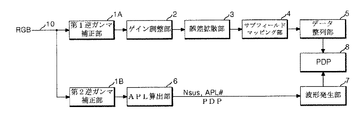
図13及び図14を参照すれば、本発明の実施形態に係るPDPの初期化制御装置は、第1逆ガンマ補正部1Aとデータ整列部5との間に接続されたゲイン調整部2、誤差拡散部3及びサブフィールドマッピング部4と、第2逆ガンマ補正部1Bと波形発生部7との間に接続されたAPL算出部6と、を備える。
Referring to FIGS. 13 and 14, the PDP initialization control apparatus according to the embodiment of the present invention includes a
第1及び第2逆ガンマ補正部1A、1Bは、入力ライン10からのデジタルビデオデータRGBを逆ガンマ補正して映像信号の階調値に対する輝度を線形的に変換させる。
The first and second inverse
ゲイン調整部2は、赤色、緑色及び青色の各データ別に有効利得を調整して色温度を補償する。
The
誤差拡散部3は、ゲイン調整部2から入力されるデジタルビデオデータの量子化誤差を隣接したセルに拡散させることにより、輝度値を微細に調整する。このために、誤差拡散部3はデータを整数部と小数部に分けて小数部にフロイド・シュタインベルグ(Floyd-Steinberg)係数をかける。
The
サブフィールドマッピング部4は、誤差拡散部3から入力されたデータを各ビット別に予め保存されたサブフィールドパターンにマッピングし、そのマッピングデータをデータ整列部5に供給する。
The
データ整列部5は、サブフィールドマッピング部4から入力されるデジタルビデオデータをPDP8のデータ駆動部102に供給する。データ駆動部102は、PDP8のアドレス電極X1〜Xmに接続され、データ整列部5から入力されるデータを1水平ライン分ずつラッチした後、ラッチされたデータを1水平期間単位でアドレス電極X1〜Xmに供給する。
The
APL算出部6は、第2逆ガンマ補正部1Bから入力されるデジタルビデオデータに対して1画面単位でAPLを算出し、算出されたAPLに対応するサステインパルス数データNsusを出力する。また、APL算出部6は、算出されたAPLが含まれるAPL群の識別データAPL#を出力する。このために、APL算出部6は、図15のようにAPLに対応するサステインパルス数データNsusが搭載されたルックアップテーブルを検索し、サステインパルス数データNsusとAPL群の識別データAPL#を読み出す。
The
波形発生部7は、図14のようにタイミングコントローラ101、駆動電圧発生部105、スキャン駆動部103及びサステイン駆動部104を備える。
The
タイミングコントローラ101は、垂直/水平同期信号H、Vとクロック信号CLKを利用して各駆動部102、103、104に必要なタイミング制御信号Cx、Cy、Czを発生させ、そのタイミング制御信号Cx、Cy、Czを当該駆動部102、103、104に供給することにより、各駆動部102、103、104を制御する。
The
データ制御信号Cxには、データをサンプリングするためのサンプリングクロック、ラッチ制御信号、エネルギー回収回路と駆動スィッチ素子のオン/オフタイムを制御するためのスィッチ制御信号が含まれる。スキャン制御信号Cyには、スキャン駆動部103内のエネルギー回収回路と駆動スィッチ素子のオン/オフタイムを制御するためのスィッチ制御信号が含まれる。サステイン制御信号Czには、サステイン駆動部104内のエネルギー回収回路と駆動スィッチ素子のオン/オフタイムを制御するためのスィッチ制御信号が含まれる
タイミングコントローラ101は、サステインパルス数データNsusによってスキャン制御信号Cyとサステイン制御信号Czを調整することにより、APLによってサステインパルス数を制御し、APL群識別データAPL#に応答して、前述した実施形態のように上昇ランプ信号Ramp−upを省略するか、そのセットアップ電圧Vsetupを調整する。
The data control signal Cx includes a sampling clock for sampling data, a latch control signal, and a switch control signal for controlling on / off times of the energy recovery circuit and the drive switch element. The scan control signal Cy includes a switch control signal for controlling the on / off time of the energy recovery circuit and the drive switch element in the
スキャン駆動部103は、タイミングコントローラ101の制御下でスキャン電極Y1〜Ymに対し、リセット期間中に上昇ランプ信号Ramp−upと降下ランプ信号Ramp−dnを供給し、アドレス期間中にスキャンパルスscanを順次供給する。また、スキャン駆動部103は、タイミングコントローラ101の制御下でスキャン電極Y1〜Ynにサステイン期間中にサステインパルスsus1、sus3、sus5を供給する。特に、スキャン駆動部103は、タイミングコントローラ101の制御下で前述した実施形態のようにAPLによって選択的に少なくとも一部サブフィールドで上昇ランプ信号Ramp−upを省略するか、上昇ランプ信号Ramp−upのセットアップ電圧Vsetup1〜Vsetupnを調整する。
The
サステイン駆動部104は、タイミングコントローラ101の制御下でアドレス期間中に直流バイアス電圧Vz−biasを供給した後、サステイン期間中にスキャン駆動部103と交互に動作してサステインパルスsus2、sus4、sus6を供給する。
The sustain
駆動電圧発生部105は、上昇ランプ信号Ruy、Ruzのセットアップ電圧Vsetup1〜Vsetupn、スキャン電圧で設定される負極性のスキャンバイアス電圧−Vy、直流バイアス電圧(Vy−bias、Vz−bias)、サステイン電圧Vs、データ電圧Vdなどを発生させる。このような駆動電圧は放電ガスの組成や放電セル構造によって変わることができる。
The
上述したように、本発明に係るPDPの初期化制御方法及び装置は、APLが基準値より低い時及び/または高い時、上昇ランプ信号を省略するか、そのセットアップ電圧を低下させる。その結果、本発明は、初期化放電数を減らすか、初期化放電を弱くして放電時に伴わう光放出量を減らすことにより、ブラック輝度を低めてコントラスト比を向上させ且つリセット期間を減らすことができる。 As described above, the PDP initialization control method and apparatus according to the present invention omits the rising ramp signal or lowers its setup voltage when the APL is lower and / or higher than the reference value. As a result, the present invention reduces the black luminance, improves the contrast ratio, and reduces the reset period by reducing the number of initializing discharges or weakening the initializing discharge to reduce the amount of light emission accompanying the discharge. Can do.
一方、本発明は、APLによって上昇ランプ波形の数やそのセットアップ電圧を調節することを中心として実施形態を説明したが、上昇ランプ波形の勾配をAPLによって制御するか、降下ランプ波形の数や電圧をAPLによって制御することもできる。 On the other hand, although the present invention has been described mainly with respect to adjusting the number of rising ramp waveforms and the setup voltage thereof by APL, the slope of the rising ramp waveform is controlled by APL, or the number and voltage of falling ramp waveforms are controlled. Can also be controlled by APL.
Claims (22)
前記入力映像の平均明るさが以前映像の平均明るさより低い時、前記初期化信号が省略されるサブフィールドの数を増加させるか、前記初期化信号の電圧が低いサブフィールドの数を増加させる段階と、を含むことを特徴とするプラズマディスプレイパネルの初期化制御方法。 Time-dividing one frame period into a plurality of subfields in which an initialization signal for generating an initialization discharge can be omitted depending on the average brightness of an input image or the voltage of the initialization signal can be adjusted; ,
When the average brightness of the input image is lower than the average brightness of the previous image, increasing the number of subfields in which the initialization signal is omitted or increasing the number of subfields in which the voltage of the initialization signal is low An initialization control method for a plasma display panel, comprising:
前記入力映像の平均明るさが所定の基準値であれば、前記サブフィールドのそれぞれで前記初期化信号として第1信号を用いてセルの初期化を行う段階と、
前記入力映像の平均明るさが前記基準値より低ければ、前記初期化信号が省略されるサブフィールドの数を増加させるか、前記初期化信号として前記第1信号の電圧より低い第2信号を用いるサブフィールドの数を増加させる段階と、
前記入力映像の平均明るさが前記基準値より高ければ、前記初期化信号が省略されるサブフィールドの数を増加させるか、前記初期化信号として前記第1信号の電圧より低い第2信号を用いるサブフィールドの数を増加させる段階と、を含むことを特徴とするプラズマディスプレイパネルの初期化制御方法。 Time-dividing one frame period into a plurality of subfields in which an initialization signal for generating an initialization discharge can be omitted depending on the average brightness of an input image or the voltage of the initialization signal can be adjusted; ,
If the average brightness of the input video is a predetermined reference value, initializing a cell using the first signal as the initialization signal in each of the subfields;
If the average brightness of the input image is lower than the reference value, the number of subfields in which the initialization signal is omitted is increased, or a second signal lower than the voltage of the first signal is used as the initialization signal. Increasing the number of subfields;
If the average brightness of the input video is higher than the reference value, the number of subfields in which the initialization signal is omitted is increased, or a second signal lower than the voltage of the first signal is used as the initialization signal. Increasing the number of subfields, and a method for controlling initialization of a plasma display panel.
前記入力映像の平均明るさを算出するAPL算出部と、
前記APL算出部によって算出された前記入力映像の平均明るさが以前映像の平均明るさより低い時、前記初期化信号が省略されるサブフィールドの数を増加させるか、前記初期化信号の電圧が低いサブフィールドの数を増加させる初期化制御部と、を備えることを特徴とするプラズマディスプレイパネルの初期化制御装置。 The initialization signal for causing the initialization discharge can be omitted depending on the average brightness of the input image, or the plasma display panel driven in a time-sharing manner into a plurality of subfields in which the voltage of the initialization signal can be adjusted is initialized. An initialization control device that
An APL calculation unit for calculating an average brightness of the input video;
When the average brightness of the input image calculated by the APL calculation unit is lower than the average brightness of the previous image, the number of subfields in which the initialization signal is omitted is increased or the voltage of the initialization signal is low An initialization control device for a plasma display panel, comprising: an initialization control unit that increases the number of subfields.
前記入力映像の平均明るさを算出するAPL算出部と、
前記APL算出部によって算出された前記入力映像の平均明るさが所定の基準値であれば、前記サブフィールドのそれぞれで前記初期化信号として第1信号を前記プラズマディスプレイパネルに供給する第1初期化制御部と、
前記入力映像の平均明るさが前記基準値より低ければ、前記初期化信号が省略されるサブフィールドの数を増加させるか、前記初期化信号として前記第1信号の電圧より低い第2信号を用いるサブフィールドの数を増加させる第2初期化制御部と、
前記入力映像の平均明るさが前記基準値より高ければ、前記初期化信号が省略されるサブフィールドの数を増加させるか、前記初期化信号として前記第1信号の電圧より低い第2信号を用いるサブフィールドの数を増加させる第3初期化制御部と、を備えることを特徴とするプラズマディスプレイパネルの初期化制御装置。 The initialization signal for causing the initialization discharge can be omitted depending on the average brightness of the input image, or the plasma display panel driven in a time-sharing manner into a plurality of subfields in which the voltage of the initialization signal can be adjusted is initialized. An initialization control device that
An APL calculation unit for calculating an average brightness of the input video;
If the average brightness of the input image calculated by the APL calculation unit is a predetermined reference value, a first initialization is performed to supply the first signal to the plasma display panel as the initialization signal in each of the subfields. A control unit;
If the average brightness of the input image is lower than the reference value, the number of subfields in which the initialization signal is omitted is increased, or a second signal lower than the voltage of the first signal is used as the initialization signal. A second initialization control unit for increasing the number of subfields;
If the average brightness of the input video is higher than the reference value, the number of subfields in which the initialization signal is omitted is increased, or a second signal lower than the voltage of the first signal is used as the initialization signal. A plasma display panel initialization control apparatus, comprising: a third initialization control unit that increases the number of subfields.
前記初期化信号を発生させる初期化信号発生部と、
前記APLによって算出された平均明るさ信号に応答して前記初期化信号発生部を制御するための制御部と、を備えることを特徴とする請求項4または5記載のプラズマディスプレイパネルの初期化制御装置。 The initialization control unit
An initialization signal generator for generating the initialization signal;
6. An initialization control for a plasma display panel according to claim 4, further comprising a control unit for controlling the initialization signal generation unit in response to an average brightness signal calculated by the APL. apparatus.
1フレーム期間を、入力映像の平均明るさによって初期化放電を起こすための初期化信号が省略可能である複数のサブフィールドに時分割する段階と、
前記入力映像の平均明るさが低下するほど、前記初期化信号を省略するサブフレーム数を増加する段階と、
を含むことを特徴とするプラズマディスプレイパネルの初期化制御方法。 (Table 1)
A step of time-dividing one frame period into a plurality of subfields in which an initialization signal for causing an initialization discharge according to the average brightness of the input video can be omitted;
Increasing the number of subframes omitting the initialization signal as the average brightness of the input video decreases;
An initialization control method for a plasma display panel, comprising:
1フレーム期間を、入力映像の平均明るさによって初期化放電を起こすための初期化信号が省略可能である複数のサブフィールドに時分割する段階と、
前記入力映像の平均明るさが所定の基準値範囲であれば1フレームの全サブフィールドで初期化信号を印加する段階と、
前記入力映像の平均明るさが所定の基準値範囲から低くなるほど、初期化信号を省略するサブフレーム数を増加させる段階と、
前記入力信号の平均の明るさが所定の基準値範囲から高くなるほど、初期化信号を省略するサブフレーム数を増加させる段階と、
を含むことを特徴とするプラズマディスプレイパネルの初期化制御方法。 (Table 2)
A step of time-dividing one frame period into a plurality of subfields in which an initialization signal for causing an initialization discharge according to the average brightness of the input video can be omitted;
Applying an initialization signal in all subfields of one frame if the average brightness of the input video is within a predetermined reference value range;
Increasing the number of subframes omitting the initialization signal as the average brightness of the input video decreases from a predetermined reference value range;
Increasing the number of subframes omitting the initialization signal as the average brightness of the input signal increases from a predetermined reference value range;
An initialization control method for a plasma display panel, comprising:
1フレーム期間を、入力映像の平均明るさによって初期化放電を起こすための初期化信号の電圧が調節可能である複数のサブフィールドに時分割する段階と、
前記入力映像の平均明るさが低下するほど前記初期化信号を低下させる段階と、
を含むことを特徴とするプラズマディスプレイパネルの初期化制御方法。 (Table 3)
Time-dividing one frame period into a plurality of subfields in which the voltage of an initialization signal for generating an initialization discharge can be adjusted according to the average brightness of the input video;
Reducing the initialization signal as the average brightness of the input video decreases;
An initialization control method for a plasma display panel, comprising:
前記初期化信号を低下させる段階では、前記最初のサブフィールド以外のサブフィールドにおいて、前記第1信号の電圧よりも低い電圧の第2信号の初期化信号が印加され、前記入力映像の平均明るさが低下するほど前記第2信号が低下されることを特徴とする、請求項12に記載のプズマディスプレイパネルの初期化制御方法。 Applying an initialization signal of the first signal in the first subfield of one frame;
In the step of reducing the initialization signal, an initialization signal of a second signal having a voltage lower than the voltage of the first signal is applied in a subfield other than the first subfield, and the average brightness of the input image The method of claim 12, wherein the second signal is reduced as the signal decreases.
1フレーム期間を、入力映像の平均明るさによって初期化放電を起こすための初期化信号の電圧が調節可能である複数のサブフィールドに時分割する段階と、
前記入力映像の平均明るさが所定値より低下するほど前記初期化信号を低下させ、前記入力映像の平均明るさが所定値より増加するほど前記初期化信号を低下させる段階と、
を含むことを特徴とするプズマディスプレイパネルの初期化制御方法。 (Table 4)
Time-dividing one frame period into a plurality of subfields in which the voltage of an initialization signal for generating an initialization discharge can be adjusted according to the average brightness of the input video;
Reducing the initialization signal as the average brightness of the input video falls below a predetermined value, and lowering the initialization signal as the average brightness of the input video rises above a predetermined value;
A method for controlling initialization of a Puzma display panel, comprising:
前記初期化信号を低下させる段階では、前記最初のサブフィールド以外のサブフィールドにおいて、前記第1信号の電圧よりも低い電圧の第2信号の初期化信号が印加され、前記入力映像の平均明るさが所定値より低下するほど前記第2信号の電圧を低下させ前記入力映像の平均明るさが所定値より増加するほど前記第2信号の電圧を低下させることを特徴とする、請求項14に記載のプラズマディスプレイパネルの初期化制御方法。 Applying an initialization signal of the first signal in the first subfield of one frame;
In the step of reducing the initialization signal, an initialization signal of a second signal having a voltage lower than the voltage of the first signal is applied in a subfield other than the first subfield, and the average brightness of the input image 15. The voltage of the second signal is decreased as the voltage decreases from a predetermined value, and the voltage of the second signal is decreased as the average brightness of the input image increases from a predetermined value. Initialization control method for plasma display panel.
1フレーム期間を、入力映像の平均明るさによって初期化放電を起こすための初期化信号が省略可能であるか、前記初期化信号の電圧が調節可能である複数のサブフィールドに時分割する段階と、
前記入力信号の平均の明るさが低くなるほど、前記初期化信号を省略又は低下するサブフィールド数を増加させるか、或いは、前記初期化信号を低下させる段階と、
を含むことを特徴とするプラズマディスプレイパネルの初期化制御方法。 (Table 5, Table 6)
Time-dividing one frame period into a plurality of subfields in which an initialization signal for generating an initialization discharge can be omitted depending on the average brightness of an input image or the voltage of the initialization signal can be adjusted; ,
Decreasing the average brightness of the input signal, increasing the number of subfields that omit or reduce the initialization signal, or reducing the initialization signal;
An initialization control method for a plasma display panel, comprising:
前記初期化信号を省略又は低下するサブフィールド数を増加させるか、或いは、前記初期化信号を低下させる段階は、
前記入力映像の平均明るさが所定値未満である場合には、前記入力信号の平均の明るさが低下するほど、前記初期化信号を低下させ、前記入力映像の平均明るさが所定値以上である場合には、前記入力信号の平均の明るさが増加するほど、前記初期化信号を省略又は低下するサブフィールド数を減少させることを特徴とする、請求項16に記載のプラズマディスプレイパネルの初期化制御方法。 (Table 5)
Increasing the number of subfields that omit or reduce the initialization signal, or reducing the initialization signal,
When the average brightness of the input video is less than a predetermined value, the initialization signal is decreased as the average brightness of the input signal decreases, and the average brightness of the input video is equal to or higher than a predetermined value. 17. The plasma display panel initial stage of claim 16, wherein in some cases, as the average brightness of the input signal increases, the number of subfields in which the initialization signal is omitted or reduced is decreased. Control method.
前記初期化信号を省略するサブフィールド数を増加させるか、又は、前記初期化信号を低下させる段階は、
前記入力映像の平均明るさが所定値未満である場合には、前記入力信号の平均の明るさが低下するほど、前記初期化信号を省略又は低下するサブフィールド数を増加させる段階と、
前記入力映像の平均明るさが所定値以上である場合には、前記入力信号の平均の明るさが増加するほど、前記初期化信号を高くする段階と、
を含むことを特徴とするプラズマディスプレイパネルの初期化制御方法。 (Table 6)
Increasing the number of subfields omitting the initialization signal, or decreasing the initialization signal,
When the average brightness of the input video is less than a predetermined value, the step of omitting the initialization signal or increasing the number of subfields as the average brightness of the input signal decreases;
If the average brightness of the input video is greater than or equal to a predetermined value, increasing the initialization signal as the average brightness of the input signal increases; and
An initialization control method for a plasma display panel, comprising:
前記初期化信号を省略又は低下するサブフィールド数を増加させるか、或いは、前記初期化信号を低下させる段階は、前記最初のフレーム以外のフレームで実行され、前記第1信号の電圧よりも低い第2信号が初期化信号として印加されることを特徴とする、請求項16乃至18の何れかに記載のプラズマディスプレイパネルの初期化制御方法。 Further comprising applying an initialization signal of the first signal in the first frame of one frame;
The step of increasing or decreasing the number of subfields omitting or reducing the initialization signal or reducing the initialization signal is performed in a frame other than the first frame and is lower than a voltage of the first signal. 19. The method for controlling initialization of a plasma display panel according to claim 16, wherein two signals are applied as initialization signals.
1フレーム期間を、入力映像の平均明るさによって初期化放電を起こすための初期化信号が省略可能であるか、前記初期化信号の電圧が調節可能である複数のサブフィールドに時分割する段階と、
前記入力映像の平均明るさが前記第1所定値から前記第1所定値未満の第2所定値まで低くなるほど、前記初期化信号を省略又は低下するサブフィールド数を増加する段階と、
前記入力映像の平均明るさが前記第2所定値より低くなるほど、前記初期化信号を低下させる段階と、
前記入力映像の平均明るさが前記第1所定値から前記第1所定値より大きい第3所定値まで高くなるほど、前記初期化信号を省略又は低下するサブフィールド数を増加する段階と、
前記入力映像の平均明るさが前記第3所定値より高くなるほど、前記初期化信号を低下させる段階と、
を含むことを特徴とするプラズマディスプレイパネルの初期化制御方法。 (Table 7)
Time-dividing one frame period into a plurality of subfields in which an initialization signal for generating an initialization discharge can be omitted depending on the average brightness of an input image or the voltage of the initialization signal can be adjusted; ,
Increasing the number of subfields in which the initialization signal is omitted or reduced as the average brightness of the input image decreases from the first predetermined value to a second predetermined value less than the first predetermined value;
Lowering the initialization signal as the average brightness of the input video is lower than the second predetermined value;
Increasing the number of subfields that omit or reduce the initialization signal as the average brightness of the input video increases from the first predetermined value to a third predetermined value that is greater than the first predetermined value;
Reducing the initialization signal as the average brightness of the input video is higher than the third predetermined value;
An initialization control method for a plasma display panel, comprising:
前記各段階は、前記最初のフレーム以外のフレームで実行されることを特徴とする、請求項20に記載のプラズマディスプレイパネルの初期化制御方法。 Further comprising applying an initialization signal of the first signal in the first frame of one frame;
The method of claim 20, wherein each of the steps is performed in a frame other than the first frame.
Applications Claiming Priority (1)
| Application Number | Priority Date | Filing Date | Title |
|---|---|---|---|
| KR10-2003-0079783A KR100524312B1 (en) | 2003-11-12 | 2003-11-12 | Method and apparatus for controling initialization in plasma display panel |
Publications (2)
| Publication Number | Publication Date |
|---|---|
| JP2005148746A true JP2005148746A (en) | 2005-06-09 |
| JP2005148746A5 JP2005148746A5 (en) | 2007-12-27 |
Family
ID=34431754
Family Applications (1)
| Application Number | Title | Priority Date | Filing Date |
|---|---|---|---|
| JP2004329451A Ceased JP2005148746A (en) | 2003-11-12 | 2004-11-12 | Method and apparatus for controlling initialization ofin plasma display panel |
Country Status (6)
| Country | Link |
|---|---|
| US (1) | US20050162344A1 (en) |
| EP (1) | EP1531451A3 (en) |
| JP (1) | JP2005148746A (en) |
| KR (1) | KR100524312B1 (en) |
| CN (1) | CN1617199A (en) |
| TW (1) | TWI293442B (en) |
Cited By (7)
| Publication number | Priority date | Publication date | Assignee | Title |
|---|---|---|---|---|
| JP2006317857A (en) * | 2005-05-16 | 2006-11-24 | Matsushita Electric Ind Co Ltd | Method for driving plasma display panel |
| JP2006317856A (en) * | 2005-05-16 | 2006-11-24 | Matsushita Electric Ind Co Ltd | Method for driving plasma display panel |
| WO2007094294A1 (en) * | 2006-02-14 | 2007-08-23 | Matsushita Electric Industrial Co., Ltd. | Method for driving plasma display panel and plasma display device |
| WO2008001470A1 (en) * | 2006-06-30 | 2008-01-03 | Hitachi Plasma Display Limited | Plasma display device |
| WO2008018527A1 (en) * | 2006-08-10 | 2008-02-14 | Panasonic Corporation | Plasma display device and plasma display panel drive method |
| JP2009042722A (en) * | 2007-08-08 | 2009-02-26 | Samsung Sdi Co Ltd | Plasma display device and driving method thereof |
| JPWO2008018370A1 (en) * | 2006-08-10 | 2009-12-24 | パナソニック株式会社 | Plasma display apparatus and driving method of plasma display panel |
Families Citing this family (19)
| Publication number | Priority date | Publication date | Assignee | Title |
|---|---|---|---|---|
| SG124351A1 (en) | 2005-01-14 | 2006-08-30 | Asml Netherlands Bv | Lithographic apparatus and device manufacturing method |
| KR100605763B1 (en) * | 2005-01-18 | 2006-08-01 | 엘지전자 주식회사 | Driving Apparatus and Method for Plasma Display Panel |
| JP2006235106A (en) * | 2005-02-23 | 2006-09-07 | Fujitsu Hitachi Plasma Display Ltd | Plasma display device |
| KR100667539B1 (en) * | 2005-04-07 | 2007-01-12 | 엘지전자 주식회사 | Plasma Display Apparatus and Driving Method thereof |
| JP4992195B2 (en) * | 2005-04-13 | 2012-08-08 | パナソニック株式会社 | Plasma display panel driving method and plasma display device |
| JP2006293113A (en) * | 2005-04-13 | 2006-10-26 | Matsushita Electric Ind Co Ltd | Driving method of plasma display panel, and plasma display device |
| KR100667538B1 (en) * | 2005-05-30 | 2007-01-12 | 엘지전자 주식회사 | Plasma Display Apparatus and Driving Method Thereof |
| KR100692824B1 (en) * | 2005-06-24 | 2007-03-09 | 엘지전자 주식회사 | Apparatus and method for driving plasma display panel |
| KR100667321B1 (en) * | 2005-09-27 | 2007-01-12 | 엘지전자 주식회사 | Plasma display apparatus and driving method thereof |
| KR100713651B1 (en) * | 2005-10-28 | 2007-05-02 | 엘지전자 주식회사 | Plasma display panel driving apparatus and method for reducing misfiring and improving contrast |
| KR20070047551A (en) * | 2005-11-02 | 2007-05-07 | 엘지전자 주식회사 | Plasma display device |
| KR100775824B1 (en) | 2005-11-28 | 2007-11-13 | 엘지전자 주식회사 | Plasma display device |
| US7705842B2 (en) * | 2006-01-11 | 2010-04-27 | Microsoft Corporation | Fast display initialization and light up |
| CN101317207B (en) * | 2006-02-24 | 2010-09-22 | 松下电器产业株式会社 | Method for driving plasma display panel, and plasma display |
| KR100844834B1 (en) * | 2007-02-09 | 2008-07-08 | 엘지전자 주식회사 | Driving method for plasma display apparatus |
| US8446399B2 (en) * | 2007-09-03 | 2013-05-21 | Panasonic Corporation | Driving device and driving method of plasma display panel, and plasma display apparatus |
| KR100903647B1 (en) * | 2007-10-26 | 2009-06-18 | 엘지전자 주식회사 | Apparatus for driving plasma display panel and plasma display apparatus thereof |
| JP2009193019A (en) * | 2008-02-18 | 2009-08-27 | Hitachi Ltd | Driving method for plasma display panel and plasma display apparatus |
| US20100207932A1 (en) * | 2009-02-17 | 2010-08-19 | Seung-Won Choi | Plasma display and driving method thereof |
Citations (11)
| Publication number | Priority date | Publication date | Assignee | Title |
|---|---|---|---|---|
| JPH11231833A (en) * | 1997-12-10 | 1999-08-27 | Matsushita Electric Ind Co Ltd | Driving pulse control device for pdp display |
| JPH11231825A (en) * | 1997-12-10 | 1999-08-27 | Matsushita Electric Ind Co Ltd | Display device capable of adjusting the number of subfields according to brightness |
| JP2000221940A (en) * | 1999-01-28 | 2000-08-11 | Mitsubishi Electric Corp | Driving device of plasma display panel and driving method therefor |
| JP2001255847A (en) * | 2000-03-10 | 2001-09-21 | Nec Corp | Method for driving plasma display panel |
| JP2001337646A (en) * | 2000-05-24 | 2001-12-07 | Pioneer Electronic Corp | Plasma display panel drive method |
| JP2002328648A (en) * | 2001-04-26 | 2002-11-15 | Nec Corp | Method and device for driving ac type plasma display panel |
| JP2002351394A (en) * | 2001-05-29 | 2002-12-06 | Pioneer Electronic Corp | Driving device for plasma display device |
| JP2003015584A (en) * | 2001-06-27 | 2003-01-17 | Pioneer Electronic Corp | Drive method for plasma display panel |
| JP2003167549A (en) * | 2001-12-03 | 2003-06-13 | Pioneer Electronic Corp | Driving device for plasma display panel |
| JP2003177695A (en) * | 2001-12-10 | 2003-06-27 | Pioneer Electronic Corp | Method and device for driving plasma display panel |
| JP2003216094A (en) * | 2002-01-18 | 2003-07-30 | Pioneer Electronic Corp | Method and device for driving plasma display panel |
Family Cites Families (6)
| Publication number | Priority date | Publication date | Assignee | Title |
|---|---|---|---|---|
| JP2002132208A (en) * | 2000-10-27 | 2002-05-09 | Fujitsu Ltd | Driving method and driving circuit for plasma display panel |
| KR100404839B1 (en) * | 2001-05-15 | 2003-11-07 | 엘지전자 주식회사 | Addressing Method and Apparatus of Plasma Display Panel |
| US6630796B2 (en) * | 2001-05-29 | 2003-10-07 | Pioneer Corporation | Method and apparatus for driving a plasma display panel |
| KR100472359B1 (en) * | 2001-11-28 | 2005-02-21 | 엘지전자 주식회사 | Setting method of average picture level |
| EP1316938A3 (en) | 2001-12-03 | 2008-06-04 | Pioneer Corporation | Driving device for plasma display panel |
| KR100508250B1 (en) * | 2003-06-05 | 2005-08-18 | 엘지전자 주식회사 | Driving method of plasma display panel |
-
2003
- 2003-11-12 KR KR10-2003-0079783A patent/KR100524312B1/en not_active IP Right Cessation
-
2004
- 2004-11-10 TW TW093134279A patent/TWI293442B/en not_active IP Right Cessation
- 2004-11-12 JP JP2004329451A patent/JP2005148746A/en not_active Ceased
- 2004-11-12 EP EP04257036A patent/EP1531451A3/en not_active Withdrawn
- 2004-11-12 US US10/986,157 patent/US20050162344A1/en not_active Abandoned
- 2004-11-12 CN CNA2004100926887A patent/CN1617199A/en active Pending
Patent Citations (11)
| Publication number | Priority date | Publication date | Assignee | Title |
|---|---|---|---|---|
| JPH11231833A (en) * | 1997-12-10 | 1999-08-27 | Matsushita Electric Ind Co Ltd | Driving pulse control device for pdp display |
| JPH11231825A (en) * | 1997-12-10 | 1999-08-27 | Matsushita Electric Ind Co Ltd | Display device capable of adjusting the number of subfields according to brightness |
| JP2000221940A (en) * | 1999-01-28 | 2000-08-11 | Mitsubishi Electric Corp | Driving device of plasma display panel and driving method therefor |
| JP2001255847A (en) * | 2000-03-10 | 2001-09-21 | Nec Corp | Method for driving plasma display panel |
| JP2001337646A (en) * | 2000-05-24 | 2001-12-07 | Pioneer Electronic Corp | Plasma display panel drive method |
| JP2002328648A (en) * | 2001-04-26 | 2002-11-15 | Nec Corp | Method and device for driving ac type plasma display panel |
| JP2002351394A (en) * | 2001-05-29 | 2002-12-06 | Pioneer Electronic Corp | Driving device for plasma display device |
| JP2003015584A (en) * | 2001-06-27 | 2003-01-17 | Pioneer Electronic Corp | Drive method for plasma display panel |
| JP2003167549A (en) * | 2001-12-03 | 2003-06-13 | Pioneer Electronic Corp | Driving device for plasma display panel |
| JP2003177695A (en) * | 2001-12-10 | 2003-06-27 | Pioneer Electronic Corp | Method and device for driving plasma display panel |
| JP2003216094A (en) * | 2002-01-18 | 2003-07-30 | Pioneer Electronic Corp | Method and device for driving plasma display panel |
Cited By (17)
| Publication number | Priority date | Publication date | Assignee | Title |
|---|---|---|---|---|
| JP2006317856A (en) * | 2005-05-16 | 2006-11-24 | Matsushita Electric Ind Co Ltd | Method for driving plasma display panel |
| JP2006317857A (en) * | 2005-05-16 | 2006-11-24 | Matsushita Electric Ind Co Ltd | Method for driving plasma display panel |
| JP4736530B2 (en) * | 2005-05-16 | 2011-07-27 | パナソニック株式会社 | Driving method of plasma display panel |
| WO2007094294A1 (en) * | 2006-02-14 | 2007-08-23 | Matsushita Electric Industrial Co., Ltd. | Method for driving plasma display panel and plasma display device |
| JP2007249176A (en) * | 2006-02-14 | 2007-09-27 | Matsushita Electric Ind Co Ltd | Driving method of plasma display panel, and plasma display device |
| KR100885593B1 (en) | 2006-02-14 | 2009-02-24 | 파나소닉 주식회사 | Method for driving plasma display panel and plasma display device |
| US7995006B2 (en) | 2006-02-14 | 2011-08-09 | Panasonic Corporation | Method of driving plasma display panel, and plasma display device |
| KR100953249B1 (en) | 2006-06-30 | 2010-04-16 | 히다찌 플라즈마 디스플레이 가부시키가이샤 | Plasma display device |
| WO2008001470A1 (en) * | 2006-06-30 | 2008-01-03 | Hitachi Plasma Display Limited | Plasma display device |
| US8242977B2 (en) | 2006-06-30 | 2012-08-14 | Hitachi, Ltd. | Plasma display apparatus with driving and controlling circuit unit |
| JPWO2008018370A1 (en) * | 2006-08-10 | 2009-12-24 | パナソニック株式会社 | Plasma display apparatus and driving method of plasma display panel |
| JP4530047B2 (en) * | 2006-08-10 | 2010-08-25 | パナソニック株式会社 | Plasma display apparatus and driving method of plasma display panel |
| JP4530048B2 (en) * | 2006-08-10 | 2010-08-25 | パナソニック株式会社 | Plasma display apparatus and driving method of plasma display panel |
| JPWO2008018527A1 (en) * | 2006-08-10 | 2010-01-07 | パナソニック株式会社 | Plasma display apparatus and driving method of plasma display panel |
| WO2008018527A1 (en) * | 2006-08-10 | 2008-02-14 | Panasonic Corporation | Plasma display device and plasma display panel drive method |
| US8400372B2 (en) | 2006-08-10 | 2013-03-19 | Panasonic Corporation | Plasma display device and method of driving plasma display panel |
| JP2009042722A (en) * | 2007-08-08 | 2009-02-26 | Samsung Sdi Co Ltd | Plasma display device and driving method thereof |
Also Published As
| Publication number | Publication date |
|---|---|
| TWI293442B (en) | 2008-02-11 |
| CN1617199A (en) | 2005-05-18 |
| EP1531451A2 (en) | 2005-05-18 |
| EP1531451A3 (en) | 2006-01-18 |
| KR100524312B1 (en) | 2005-10-28 |
| KR20050045636A (en) | 2005-05-17 |
| US20050162344A1 (en) | 2005-07-28 |
| TW200519815A (en) | 2005-06-16 |
Similar Documents
| Publication | Publication Date | Title |
|---|---|---|
| KR100524312B1 (en) | Method and apparatus for controling initialization in plasma display panel | |
| US7911417B2 (en) | Method and apparatus for expressing gray levels in a plasma display panel | |
| JP4636901B2 (en) | Plasma display apparatus and driving method thereof | |
| US7907103B2 (en) | Plasma display apparatus and driving method thereof | |
| KR100547979B1 (en) | Apparatus and Method of Driving Plasma Display Panel | |
| JP2008203906A (en) | Method for expressing gray scale in plasma display panel | |
| JP4181959B2 (en) | Method and apparatus for driving plasma display panel | |
| US20070030214A1 (en) | Plasma display apparatus and driving method thereof | |
| JP4160575B2 (en) | Plasma display device and driving method thereof | |
| JP2006235574A (en) | Plasma display apparatus, driving method of the same, plasma display panel and driving gear of plasma display panel | |
| JP2005196194A (en) | Method and apparatus for driving plasma display panel | |
| KR20040102407A (en) | Method and Apparatus for Driving Plasma Display Panel | |
| US7561153B2 (en) | Apparatus and method of driving plasma display panel | |
| JP4576475B2 (en) | Plasma display device and control method thereof | |
| JP2005107536A (en) | Method and apparatus for driving plasma display panel | |
| KR20040030316A (en) | Method and Apparatus of Driving Plasma Display Panel | |
| KR20040068419A (en) | Method and apparatus for driving plasma display panel | |
| KR100489281B1 (en) | Method and Apparatus of Driving Plasma Display Panel | |
| KR100488150B1 (en) | Apparatus and Method for Driving Plasma Display Panel | |
| KR100692824B1 (en) | Apparatus and method for driving plasma display panel | |
| KR100738815B1 (en) | Driving Apparatus for Plasma Display Panel and Driving Method thereof | |
| KR20090044333A (en) | Plasma display apparatus | |
| KR20030090812A (en) | Plasma display panel and driving method thereof |
Legal Events
| Date | Code | Title | Description |
|---|---|---|---|
| A521 | Written amendment |
Free format text: JAPANESE INTERMEDIATE CODE: A523 Effective date: 20071108 |
|
| A621 | Written request for application examination |
Free format text: JAPANESE INTERMEDIATE CODE: A621 Effective date: 20071108 |
|
| A131 | Notification of reasons for refusal |
Free format text: JAPANESE INTERMEDIATE CODE: A131 Effective date: 20100629 |
|
| A601 | Written request for extension of time |
Free format text: JAPANESE INTERMEDIATE CODE: A601 Effective date: 20100929 |
|
| A602 | Written permission of extension of time |
Free format text: JAPANESE INTERMEDIATE CODE: A602 Effective date: 20101004 |
|
| A521 | Written amendment |
Free format text: JAPANESE INTERMEDIATE CODE: A523 Effective date: 20101007 |
|
| A131 | Notification of reasons for refusal |
Free format text: JAPANESE INTERMEDIATE CODE: A131 Effective date: 20101109 |
|
| A521 | Written amendment |
Free format text: JAPANESE INTERMEDIATE CODE: A523 Effective date: 20110204 |
|
| A131 | Notification of reasons for refusal |
Free format text: JAPANESE INTERMEDIATE CODE: A131 Effective date: 20110301 |
|
| A521 | Written amendment |
Free format text: JAPANESE INTERMEDIATE CODE: A523 Effective date: 20110530 |
|
| A01 | Written decision to grant a patent or to grant a registration (utility model) |
Free format text: JAPANESE INTERMEDIATE CODE: A01 Effective date: 20120612 |
|
| A045 | Written measure of dismissal of application [lapsed due to lack of payment] |
Free format text: JAPANESE INTERMEDIATE CODE: A045 Effective date: 20121030 |