JP2005136383A - Organic semiconductor device, manufacturing method of the same and organic semiconductor device - Google Patents
Organic semiconductor device, manufacturing method of the same and organic semiconductor device Download PDFInfo
- Publication number
- JP2005136383A JP2005136383A JP2004264499A JP2004264499A JP2005136383A JP 2005136383 A JP2005136383 A JP 2005136383A JP 2004264499 A JP2004264499 A JP 2004264499A JP 2004264499 A JP2004264499 A JP 2004264499A JP 2005136383 A JP2005136383 A JP 2005136383A
- Authority
- JP
- Japan
- Prior art keywords
- organic semiconductor
- polymer layer
- semiconductor element
- insulating film
- layer
- Prior art date
- Legal status (The legal status is an assumption and is not a legal conclusion. Google has not performed a legal analysis and makes no representation as to the accuracy of the status listed.)
- Pending
Links
- 0 CCC(C)(C)C(C1(*)C(C)(CC)C2)c3cccc4ccc2c1c34 Chemical compound CCC(C)(C)C(C1(*)C(C)(CC)C2)c3cccc4ccc2c1c34 0.000 description 1
Images

Classifications
-
- H—ELECTRICITY
- H01—ELECTRIC ELEMENTS
- H01L—SEMICONDUCTOR DEVICES NOT COVERED BY CLASS H10
- H01L21/00—Processes or apparatus adapted for the manufacture or treatment of semiconductor or solid state devices or of parts thereof
- H01L21/02—Manufacture or treatment of semiconductor devices or of parts thereof
- H01L21/02104—Forming layers
- H01L21/02107—Forming insulating materials on a substrate
- H01L21/02109—Forming insulating materials on a substrate characterised by the type of layer, e.g. type of material, porous/non-porous, pre-cursors, mixtures or laminates
- H01L21/02112—Forming insulating materials on a substrate characterised by the type of layer, e.g. type of material, porous/non-porous, pre-cursors, mixtures or laminates characterised by the material of the layer
- H01L21/02118—Forming insulating materials on a substrate characterised by the type of layer, e.g. type of material, porous/non-porous, pre-cursors, mixtures or laminates characterised by the material of the layer carbon based polymeric organic or inorganic material, e.g. polyimides, poly cyclobutene or PVC
-
- H—ELECTRICITY
- H01—ELECTRIC ELEMENTS
- H01L—SEMICONDUCTOR DEVICES NOT COVERED BY CLASS H10
- H01L21/00—Processes or apparatus adapted for the manufacture or treatment of semiconductor or solid state devices or of parts thereof
- H01L21/02—Manufacture or treatment of semiconductor devices or of parts thereof
- H01L21/04—Manufacture or treatment of semiconductor devices or of parts thereof the devices having at least one potential-jump barrier or surface barrier, e.g. PN junction, depletion layer or carrier concentration layer
- H01L21/18—Manufacture or treatment of semiconductor devices or of parts thereof the devices having at least one potential-jump barrier or surface barrier, e.g. PN junction, depletion layer or carrier concentration layer the devices having semiconductor bodies comprising elements of Group IV of the Periodic System or AIIIBV compounds with or without impurities, e.g. doping materials
- H01L21/30—Treatment of semiconductor bodies using processes or apparatus not provided for in groups H01L21/20 - H01L21/26
- H01L21/31—Treatment of semiconductor bodies using processes or apparatus not provided for in groups H01L21/20 - H01L21/26 to form insulating layers thereon, e.g. for masking or by using photolithographic techniques; After treatment of these layers; Selection of materials for these layers
- H01L21/312—Organic layers, e.g. photoresist
-
- H—ELECTRICITY
- H10—SEMICONDUCTOR DEVICES; ELECTRIC SOLID-STATE DEVICES NOT OTHERWISE PROVIDED FOR
- H10K—ORGANIC ELECTRIC SOLID-STATE DEVICES
- H10K10/00—Organic devices specially adapted for rectifying, amplifying, oscillating or switching; Organic capacitors or resistors having a potential-jump barrier or a surface barrier
- H10K10/40—Organic transistors
- H10K10/46—Field-effect transistors, e.g. organic thin-film transistors [OTFT]
- H10K10/462—Insulated gate field-effect transistors [IGFETs]
- H10K10/466—Lateral bottom-gate IGFETs comprising only a single gate
-
- H—ELECTRICITY
- H10—SEMICONDUCTOR DEVICES; ELECTRIC SOLID-STATE DEVICES NOT OTHERWISE PROVIDED FOR
- H10K—ORGANIC ELECTRIC SOLID-STATE DEVICES
- H10K10/00—Organic devices specially adapted for rectifying, amplifying, oscillating or switching; Organic capacitors or resistors having a potential-jump barrier or a surface barrier
- H10K10/40—Organic transistors
- H10K10/46—Field-effect transistors, e.g. organic thin-film transistors [OTFT]
- H10K10/462—Insulated gate field-effect transistors [IGFETs]
- H10K10/468—Insulated gate field-effect transistors [IGFETs] characterised by the gate dielectrics
- H10K10/474—Insulated gate field-effect transistors [IGFETs] characterised by the gate dielectrics the gate dielectric comprising a multilayered structure
-
- H—ELECTRICITY
- H10—SEMICONDUCTOR DEVICES; ELECTRIC SOLID-STATE DEVICES NOT OTHERWISE PROVIDED FOR
- H10K—ORGANIC ELECTRIC SOLID-STATE DEVICES
- H10K71/00—Manufacture or treatment specially adapted for the organic devices covered by this subclass
- H10K71/60—Forming conductive regions or layers, e.g. electrodes
-
- H—ELECTRICITY
- H01—ELECTRIC ELEMENTS
- H01L—SEMICONDUCTOR DEVICES NOT COVERED BY CLASS H10
- H01L21/00—Processes or apparatus adapted for the manufacture or treatment of semiconductor or solid state devices or of parts thereof
- H01L21/02—Manufacture or treatment of semiconductor devices or of parts thereof
- H01L21/02104—Forming layers
- H01L21/02107—Forming insulating materials on a substrate
- H01L21/02225—Forming insulating materials on a substrate characterised by the process for the formation of the insulating layer
- H01L21/0226—Forming insulating materials on a substrate characterised by the process for the formation of the insulating layer formation by a deposition process
- H01L21/02282—Forming insulating materials on a substrate characterised by the process for the formation of the insulating layer formation by a deposition process liquid deposition, e.g. spin-coating, sol-gel techniques, spray coating
-
- H—ELECTRICITY
- H10—SEMICONDUCTOR DEVICES; ELECTRIC SOLID-STATE DEVICES NOT OTHERWISE PROVIDED FOR
- H10K—ORGANIC ELECTRIC SOLID-STATE DEVICES
- H10K85/00—Organic materials used in the body or electrodes of devices covered by this subclass
- H10K85/60—Organic compounds having low molecular weight
- H10K85/615—Polycyclic condensed aromatic hydrocarbons, e.g. anthracene
Abstract
Description
本発明は、有機半導体素子、その製造方法およびその有機半導体素子を有するアクティブマトリクス型表示装置、ICタグ等の有機半導体装置に関する。 The present invention relates to an organic semiconductor device, a manufacturing method thereof, an active matrix display device having the organic semiconductor device, and an organic semiconductor device such as an IC tag.
近年、有機薄膜トランジスター(以下、有機TFTと記す)は、大きな進歩を遂げてきている。有機TFTを用いる利点は、無機TFTに比べて低温でTFT製造が可能であり、可撓性基板である安価な樹脂基板が使用できることにある。この利点によって、有機TFTはスマートカード、電子タグ、およびディスプレイなどの低コストIC技術への応用が期待されている。 In recent years, organic thin film transistors (hereinafter referred to as organic TFTs) have made great progress. The advantage of using the organic TFT is that the TFT can be manufactured at a lower temperature than the inorganic TFT, and an inexpensive resin substrate which is a flexible substrate can be used. Due to this advantage, organic TFTs are expected to be applied to low-cost IC technologies such as smart cards, electronic tags, and displays.
一般的な有機TFTは、基板、ゲート電極、ゲート絶縁膜、ソース電極、ドレイン電極及び有機半導体の構成からなる。ゲート電極に印加する電圧(ゲート電圧、Vg)を変えることで、ゲート絶縁膜と有機半導体の界面の電荷量を過剰、或いは不足にし、ソース電極/有機半導体/ドレイン電極間を流れるドレイン電流値(Id)を変化させ、スイッチングを行う。 A general organic TFT is composed of a substrate, a gate electrode, a gate insulating film, a source electrode, a drain electrode, and an organic semiconductor. By changing the voltage (gate voltage, Vg) applied to the gate electrode, the charge amount at the interface between the gate insulating film and the organic semiconductor is made excessive or insufficient, and the drain current value flowing between the source electrode / organic semiconductor / drain electrode ( Switching is performed by changing Id).
有機TFTの性能を示す物理量として、移動度、オン/オフ比、ゲート電圧しきい値が用いられる。移動度は、一般的には、Id1/2 とVgが線形関係にある飽和領域における、Id1/2 −Vg曲線の傾きから算出され、電流の流れ易さの度合いを示す。オン/オフ比は、Vgを変化させた時の最小Idと最大Idの強度比で表される。ゲート電圧しきい値は、前記飽和領域における、Id1/2 −Vg曲線に接する直線のX切片で定義され、スイッチングが起こるゲート電圧を示す。 As physical quantities indicating the performance of the organic TFT, mobility, on / off ratio, and gate voltage threshold are used. The mobility is generally calculated from the slope of the Id 1/2 -Vg curve in a saturation region where Id 1/2 and Vg are in a linear relationship, and indicates the degree of ease of current flow. The on / off ratio is expressed as an intensity ratio between the minimum Id and the maximum Id when Vg is changed. The gate voltage threshold is defined by the X-intercept of the straight line that contacts the Id 1/2 -Vg curve in the saturation region, and indicates the gate voltage at which switching occurs.
有機TFTの特性の目標値としては、現行アクティブマトリクス液晶表示装置に用いられているa−SiTFTの値が考えられている。すなわち、移動度が0.3〜1cm2 /Vs、オン/オフ比が106 以上、ゲート電圧しきい値が1〜2Vである。 As the target value of the characteristics of the organic TFT, the value of the a-Si TFT used in the current active matrix liquid crystal display device is considered. That is, the mobility is 0.3 to 1 cm 2 / Vs, the on / off ratio is 10 6 or more, and the gate voltage threshold is 1 to 2V.
最近の研究により有機TFTの特性は、有機半導体の結晶性と相関があることがわかってきている。例えば、アモルファス状態の有機半導体を用いた有機TFTでは、高移動度、高オン/オフ比の両立は不可能であることが開示されている(非特許文献1参照。)。 Recent studies have shown that the characteristics of organic TFTs are correlated with the crystallinity of organic semiconductors. For example, it is disclosed that an organic TFT using an amorphous organic semiconductor cannot achieve both high mobility and a high on / off ratio (see Non-Patent Document 1).
有機TFTの特性向上に向けて、有機半導体の結晶状態や配向の改善に、さまざまな試みがなされている。一例として、有機半導体層の下に下地層を設けて、有機半導体の結晶性を向上させる試みが挙げられる。 In order to improve the characteristics of organic TFTs, various attempts have been made to improve the crystal state and orientation of organic semiconductors. As an example, there is an attempt to improve the crystallinity of the organic semiconductor by providing a base layer under the organic semiconductor layer.
特許文献1には、下地層にポリテトラフルオロエチレン(PTFE)配向膜を用いて、オリゴチオフェン化合物等の有機半導体を配向させる方法が開示されている。しかし、PTFE膜形成のためには、固体のPTFEを一定圧力でスライドさせるため、基板の大面積化が難しい。 Patent Document 1 discloses a method of aligning an organic semiconductor such as an oligothiophene compound using a polytetrafluoroethylene (PTFE) alignment film as a base layer. However, in order to form the PTFE film, since the solid PTFE is slid at a constant pressure, it is difficult to increase the area of the substrate.
非特許文献2には、ゲート絶縁膜表面に垂直配向膜の一種であるオクタデシルトリクロロシランを塗布した後、2層のペンタセン蒸着膜を形成し、高性能な有機TFTを得る方法が開示されている。しかし、この方法は、酸化ケイ素のように塩基性官能基を持つ表面にしか適応できないため、汎用性が低い。 Non-Patent Document 2 discloses a method of obtaining a high-performance organic TFT by applying octadecyltrichlorosilane, which is a kind of vertical alignment film, to the surface of a gate insulating film and then forming a two-layer pentacene vapor-deposited film. . However, since this method can be applied only to a surface having a basic functional group such as silicon oxide, its versatility is low.
特許文献2には、ゲート絶縁膜の表面にディップ法で膜厚0.3〜10nmのフッ素系ポリマー層を形成し、その上に結晶性の有機半導体を形成する有機半導体装置が示されている。しかしこの方法では有機半導体の結晶が広角X線スペクトル中に2つのピークを持つことから配向が充分ではないと考えられ、特性も十分でない。 Patent Document 2 discloses an organic semiconductor device in which a fluorine-based polymer layer having a film thickness of 0.3 to 10 nm is formed on the surface of a gate insulating film by a dipping method, and a crystalline organic semiconductor is formed thereon. . However, in this method, since the organic semiconductor crystal has two peaks in the wide-angle X-ray spectrum, it is considered that the orientation is not sufficient and the characteristics are not sufficient.
特許文献3には、アルミナゲート絶縁膜上をアルキルリン酸類で処理することにより、有機TFTの移動度を向上させる方法が示されている。この方法も適応できるゲート絶縁膜が限られるため、汎用性が低い。 Patent Document 3 discloses a method for improving the mobility of an organic TFT by treating the alumina gate insulating film with an alkyl phosphoric acid. Since this method is also applicable to limited gate insulating films, the versatility is low.
また、非特許文献3には、無機ゲート絶縁膜に、ポリメタクリル酸メチルなどの高分子層を形成することにより、有機半導体の結晶の成長を改善する方法が示されている。しかし、この方法で得られる有機TFTの特性は低く、実用には十分でない。 Non-Patent Document 3 discloses a method for improving the growth of an organic semiconductor crystal by forming a polymer layer such as polymethyl methacrylate on an inorganic gate insulating film. However, the characteristics of the organic TFT obtained by this method are low and not sufficient for practical use.
また、特許文献4には、ゲート絶縁膜と有機半導体層との間に厚さ400Å以下のフッ素を含有しない高分子層を設けた有機TFTが示されている。
本発明は、性能の高い有機TFTの素子構造、および低コストで性能の高い有機TFTの製造方法を提供するものである。また、上記有機半導体素子を用いた有機半導体装置を提供するものである。 The present invention provides an element structure of a high-performance organic TFT and a method for manufacturing a high-performance organic TFT at a low cost. Moreover, the organic semiconductor device using the said organic-semiconductor element is provided.
すなわち、本発明は、少なくとも、基板、有機半導体、ゲート絶縁膜、導電体からなり、バイアス印加のための電極を有する有機半導体素子において、ゲート絶縁膜とは別に、高分子層が有機半導体に接して設けられており、該高分子層がメタクリル酸メチルとジビニルベンゼンの共重合体、または一般式(1)または(2) That is, according to the present invention, in an organic semiconductor element including at least a substrate, an organic semiconductor, a gate insulating film, and a conductor and having an electrode for applying a bias, the polymer layer is in contact with the organic semiconductor separately from the gate insulating film. The polymer layer is a copolymer of methyl methacrylate and divinylbenzene, or a compound represented by the general formula (1) or (2)

(R11は水素原子またはアルキル基を表し、R12は置換基を有してもよいナフチル基、置換基を有してもよいカルバゾイル基または置換基を有してもよいビフェニル基を表す。nは重合度を表す。) (R 11 represents a hydrogen atom or an alkyl group, and R 12 represents a naphthyl group which may have a substituent, a carbazoyl group which may have a substituent, or a biphenyl group which may have a substituent. n represents the degree of polymerization.)
(R21は水素原子またはアルキル基を表し、芳香環上には置換基を有していてもよい。nは重合度を表す。)
で表される重合体であることを特徴とする有機半導体素子、その有機半導体素子の製造方法、およびその有機半導体素子を用いた有機半導体装置を提供するものである。ここにいう導電体とは、一般的には、ゲート電極、ソース電極、ドレイン電極であり、この場合、本発明の有機半導体素子は、電界効果型トランジスターとして用いることができる。また、一般式(1)あるいは(2)において、重合度nは、例えば、10〜1000000である。
(R 21 represents a hydrogen atom or an alkyl group, and the aromatic ring may have a substituent. N represents the degree of polymerization.)
An organic semiconductor element, a method for producing the organic semiconductor element, and an organic semiconductor device using the organic semiconductor element are provided. The conductors here are generally a gate electrode, a source electrode, and a drain electrode. In this case, the organic semiconductor element of the present invention can be used as a field effect transistor. In the general formula (1) or (2), the degree of polymerization n is, for example, 10 to 1000000.
また、高分子層が、下記一般式(3)で表される重合体であることが好ましい。 Moreover, it is preferable that a polymer layer is a polymer represented by following General formula (3).
(R31は水素原子またはアルキル基を表し、R32はナフチル基またはカルバゾイル基を表す。nは重合度を表す。) (R 31 represents a hydrogen atom or an alkyl group, R 32 represents a naphthyl group or a carbazoyl group. N represents the degree of polymerization.)
また、上記有機半導体素子の製造方法としては、少なくとも表面の一部が導電性を有する基板上に絶縁膜を形成する工程と、該絶縁膜上にメタクリル酸メチルとジビニルベンゼンとの共重合体または上記一般式(1)または(2)で表される重合体からなる高分子層を形成する工程と、該高分子層上に有機半導体層を形成する工程とを少なくとも有する有機半導体素子の製造方法、および基板上にメタクリル酸メチルとジビニルベンゼンとの共重合体または上記一般式(1)または(2)で表される重合体からなる高分子層を形成する工程と、該高分子層上に有機半導体層を形成する工程と、該有機半導体層上に絶縁膜を形成する工程とを少なくとも有する有機半導体素子の製造方法、が挙げられる。 In addition, as a method for producing the organic semiconductor element, a step of forming an insulating film on a substrate having at least a part of the surface having conductivity, a copolymer of methyl methacrylate and divinylbenzene on the insulating film, or The manufacturing method of the organic-semiconductor element which has the process of forming the polymer layer which consists of a polymer represented by the said General formula (1) or (2), and the process of forming an organic-semiconductor layer on this polymer layer at least And a step of forming a polymer layer comprising a copolymer of methyl methacrylate and divinylbenzene or a polymer represented by the general formula (1) or (2) on the substrate, and on the polymer layer Examples include a method for producing an organic semiconductor element having at least a step of forming an organic semiconductor layer and a step of forming an insulating film on the organic semiconductor layer.
前者の場合、基板の一部の導電性を有する部分は、ゲート電極足り得る。また、後者の場合、絶縁膜上にゲート電極を形成しうる。また、いずれの場合であっても、適当な位置に、少なくとも一対の互いに離間した電極(一般的には、ソース電極/ドレイン電極)を形成しうる。その形成順は、後述するような有機半導体素子の種々の形態に応じた順序となる。 In the former case, a part of the substrate having conductivity may be a gate electrode. In the latter case, a gate electrode can be formed on the insulating film. In any case, at least a pair of spaced electrodes (generally, source / drain electrodes) can be formed at appropriate positions. The order of formation is in accordance with various forms of organic semiconductor elements as will be described later.
本発明によれば、大面積基板上に均一に作製でき、ゲート電極に印加する電圧によってドレイン電流を大きく変調させることができる高い移動度を有する有機半導体素子を提供することができる。 ADVANTAGE OF THE INVENTION According to this invention, the organic-semiconductor element which has the high mobility which can be uniformly produced on a large area substrate and can modulate a drain current largely with the voltage applied to a gate electrode can be provided.
また、本発明は、動作が安定で、低電圧で駆動することが可能で素子の寿命も長く、製造方法も簡便にできる有機半導体素子を提供することができる。
また、上記の有機半導体素子を用いた、アクティブマトリクス型表示装置或いは有機半導体素子をICカード電子タグとして用いた有機半導体装置を提供することができる。
In addition, the present invention can provide an organic semiconductor element that is stable in operation, can be driven at a low voltage, has a long element life, and can be easily manufactured.
In addition, an active matrix display device using the organic semiconductor element or an organic semiconductor device using the organic semiconductor element as an IC card electronic tag can be provided.
以下、本発明を詳細に説明する。
まず、本発明で用いられる有機半導体素子の構造について説明する。
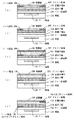
本発明で用いられる有機半導体素子の構造の例(a)〜(e)を図1に示す。図中、101は基板、102はゲート電極、103はゲート絶縁膜、104は高分子層、105は有機半導体、106はソース電極、107はドレイン電極、108は保護層を示す。保護層は必要に応じ設けられるが、省略も可能である。
Hereinafter, the present invention will be described in detail.
First, the structure of the organic semiconductor element used in the present invention will be described.
Examples (a) to (e) of the structure of the organic semiconductor element used in the present invention are shown in FIG. In the figure, 101 is a substrate, 102 is a gate electrode, 103 is a gate insulating film, 104 is a polymer layer, 105 is an organic semiconductor, 106 is a source electrode, 107 is a drain electrode, and 108 is a protective layer. The protective layer is provided as necessary, but may be omitted.
(a)基板、ゲート電極、ゲート絶縁膜、高分子層、有機半導体、ソース電極/ドレイン電極および保護層がこの順に設けられている構造(図1(a)参照)。
(b)基板、ゲート電極、ゲート絶縁膜、有機半導体、高分子層、ソース電極/ドレイン電極および保護層がこの順に設けられている構造(図1(b)参照)。
(A) A structure in which a substrate, a gate electrode, a gate insulating film, a polymer layer, an organic semiconductor, a source / drain electrode, and a protective layer are provided in this order (see FIG. 1A).
(B) A structure in which a substrate, a gate electrode, a gate insulating film, an organic semiconductor, a polymer layer, a source / drain electrode, and a protective layer are provided in this order (see FIG. 1B).
(c)基板、ゲート電極、ゲート絶縁膜、高分子層、ソース電極/ドレイン電極、有機半導体および保護層がこの順に設けられている構造(図1(c)参照)。
(d)基板、ゲート電極、ゲート絶縁膜、ソース電極/ドレイン電極、高分子層、有機半導体および保護層がこの順に設けられている構造(図1(d)参照)。
(C) A structure in which a substrate, a gate electrode, a gate insulating film, a polymer layer, a source / drain electrode, an organic semiconductor, and a protective layer are provided in this order (see FIG. 1C).
(D) A structure in which a substrate, a gate electrode, a gate insulating film, a source / drain electrode, a polymer layer, an organic semiconductor, and a protective layer are provided in this order (see FIG. 1D).
(e)基板、ゲート電極、ゲート絶縁膜、ソース電極/ドレイン電極のいずれか一方、高分子層、有機半導体、ソース電極/ドレイン電極のいずれか一方および保護層がこの順に設けられている構造(図1(e)参照)。 (E) A structure in which any one of a substrate, a gate electrode, a gate insulating film, a source electrode / drain electrode, a polymer layer, an organic semiconductor, a source electrode / drain electrode, and a protective layer are provided in this order ( (Refer FIG.1 (e)).
ただし、これらは一例であり、この形成順および配置に限定されるものではない。もっとも、高分子層を形成した後に有機半導体層を形成することが好ましい。このような形成順とすることにより高分子層が有機半導体層の配向制御層として機能するためである。 However, these are examples, and are not limited to the formation order and arrangement. However, it is preferable to form the organic semiconductor layer after forming the polymer layer. This is because the polymer layer functions as an orientation control layer of the organic semiconductor layer by adopting such an order of formation.
このような好ましい配置の構造としては、例えば、
基板に、ゲート電極、ゲート絶縁膜、高分子層、有機半導体、およびソース電極/ドレイン電極をこの順に有するもの、
基板に、ゲート電極、ゲート絶縁膜、高分子層、ソース電極/ドレイン電極、および有機半導体層をこの順に有するもの、
基板に、ゲート電極、ゲート絶縁膜、ソース電極/ドレイン電極、高分子層および有機半導体層をこの順に有するもの、
基板に、ソース電極/ドレイン電極、高分子層、有機半導体層、ゲート絶縁膜およびゲート電極をこの順に有するもの、
基板に、高分子層、ソース電極/ドレイン電極、有機半導体層、ゲート絶縁膜およびゲート電極をこの順に有するもの、
基板に、高分子層、ソース電極/ドレイン電極、有機半導体層、ゲート絶縁膜およびゲート電極をこの順に有するもの、
が挙げられる。
As a structure of such a preferable arrangement, for example,
A substrate having a gate electrode, a gate insulating film, a polymer layer, an organic semiconductor, and a source electrode / drain electrode in this order,
A substrate having a gate electrode, a gate insulating film, a polymer layer, a source / drain electrode, and an organic semiconductor layer in this order,
A substrate having a gate electrode, a gate insulating film, a source / drain electrode, a polymer layer and an organic semiconductor layer in this order;
A substrate having a source electrode / drain electrode, a polymer layer, an organic semiconductor layer, a gate insulating film and a gate electrode in this order,
A substrate having a polymer layer, a source electrode / drain electrode, an organic semiconductor layer, a gate insulating film and a gate electrode in this order;
A substrate having a polymer layer, a source electrode / drain electrode, an organic semiconductor layer, a gate insulating film and a gate electrode in this order;
Is mentioned.
また、基板に、ゲート電極、ゲート絶縁膜、ソース電極/ドレイン電極のいずれか一方、有機半導体、およびソース電極/ドレイン電極の他方、をこの順に有する有機半導体素子において、前記有機半導体に接して、高分子層を有する構造や、基板に、ソース電極/ドレイン電極のいずれか一方、有機半導体、およびソース電極/ドレイン電極の他方、ゲート絶縁膜、ゲート電極、をこの順に有する有機半導体素子において、前記有機半導体に接して、高分子層を有する構造も、本発明の範囲内であるが、これらの構造においても、高分子層の形成後にその上に有機半導体層が形成される配置とすることが好ましい。 Further, in an organic semiconductor element having, in this order, any one of a gate electrode, a gate insulating film, a source electrode / drain electrode, an organic semiconductor, and the other of the source electrode / drain electrode on the substrate, the organic semiconductor element is in contact with the organic semiconductor, In the organic semiconductor element having a structure having a polymer layer or a substrate having either one of a source electrode / drain electrode, an organic semiconductor, and the other of the source electrode / drain electrode, a gate insulating film, and a gate electrode in this order, Structures having a polymer layer in contact with an organic semiconductor are also within the scope of the present invention. However, even in these structures, the organic semiconductor layer may be formed on the polymer layer after the polymer layer is formed. preferable.
次に、本発明の有機半導体素子とその製造方法について説明する。
本発明で用いられる基板材料としては、有機、無機の様々な材料から選択が可能である。具体的には、シリコン、アルミニウム、ガラス、アルミナ焼結体などの無機材料、ポリエチレンテレフタレート、ポリエチレンナフタレート、ポリイミド、ポリエチレン、ポリプロピレン、ポリエーテルエーテルケトン、ポリスルホン、ポリフェニレンスルフィドなどの有機材料、ガラス繊維で強化された有機材料などの複合材料が挙げられる。
Next, the organic semiconductor element of the present invention and the manufacturing method thereof will be described.
The substrate material used in the present invention can be selected from various organic and inorganic materials. Specifically, inorganic materials such as silicon, aluminum, glass and alumina sintered bodies, organic materials such as polyethylene terephthalate, polyethylene naphthalate, polyimide, polyethylene, polypropylene, polyetheretherketone, polysulfone and polyphenylene sulfide, and glass fibers. Examples include composite materials such as reinforced organic materials.
本発明で用いられるゲート電極材料としては、導電性の材料から選ばれ、具体的には、金、白金、銅、銀、パラジウム、クロム、モリブデン、チタン、ニッケル、アルミなどの金属材料、錫酸化物、酸化インジウム、インジウム・錫酸化物などの非金属無機材料、ポリチオフェン、ポリアニリンなどの有機材料、カーボン材料などが挙げられる。金属材料は合金も使用可能である。基板として導電性の材料を用いた場合には、基板をゲート電極に用いることも可能である。 The gate electrode material used in the present invention is selected from conductive materials, specifically, metal materials such as gold, platinum, copper, silver, palladium, chromium, molybdenum, titanium, nickel, and aluminum, tin oxide And non-metallic inorganic materials such as indium oxide and indium / tin oxide, organic materials such as polythiophene and polyaniline, and carbon materials. An alloy can also be used as the metal material. When a conductive material is used for the substrate, the substrate can be used for the gate electrode.
本発明で用いられるゲート絶縁膜材料としては、酸化ケイ素、窒化ケイ素、アルミナ、酸化タンタルなどの無機材料、ポリメタクリル酸メチル、ポリイミド、ポリパラキシレン、ポリクロロピレン、ポリエチレンテレフタレート、ポリオキシメチレン、シルセスキオキサン、ポリビニルクロライド、ポリフッ化ビニリデン、シアノエチルプルラン、ポリサルホン、ポリカーボネイトなどの有機材料が挙げられる。 The gate insulating film material used in the present invention includes inorganic materials such as silicon oxide, silicon nitride, alumina, and tantalum oxide, polymethyl methacrylate, polyimide, polyparaxylene, polychloropyrene, polyethylene terephthalate, polyoxymethylene, silsesquiskies. Examples thereof include organic materials such as oxane, polyvinyl chloride, polyvinylidene fluoride, cyanoethyl pullulan, polysulfone, and polycarbonate.
本発明で用いられる高分子層は、メタクリル酸メチルとジビニルベンゼンの共重合体、または一般式(1)または(2)で示される化合物である。
前記高分子層が、メタクリル酸メチルとジビニルベンゼンの共重合体の場合、メタクリル酸メチル(A)とジビニルベンゼン(B)の共重合体比は、モノマーユニットの比率でA:B=1:0.001〜0.04であり、好ましくはA:B=1:0.001〜0.02である。
The polymer layer used in the present invention is a copolymer of methyl methacrylate and divinylbenzene, or a compound represented by the general formula (1) or (2).
When the polymer layer is a copolymer of methyl methacrylate and divinylbenzene, the copolymer ratio of methyl methacrylate (A) and divinylbenzene (B) is A: B = 1: 0 in terms of the ratio of monomer units. 0.001 to 0.04, preferably A: B = 1: 0.001 to 0.02.
高分子層の膜厚は5nm以上30nm以下が好ましく、該高分子層と接するゲート絶縁膜の表面粗さRaが5nm以下であることが好ましい。
前記高分子層が、一般式(1)または(2)で示される化合物の場合、R11、R21は水素原子またはアルキル基であり、アルキル基の具体的な例としては、メチル基、エチル基、n−プロピル基、iso−プロピル基、n−ブチル基、sec−ブチル基、tert−ブチル基、n−ペンチル基、n−ヘキシル基などが挙げられる。
The film thickness of the polymer layer is preferably 5 nm or more and 30 nm or less, and the surface roughness Ra of the gate insulating film in contact with the polymer layer is preferably 5 nm or less.
When the polymer layer is a compound represented by the general formula (1) or (2), R 11 and R 21 are a hydrogen atom or an alkyl group. Specific examples of the alkyl group include a methyl group, ethyl Group, n-propyl group, iso-propyl group, n-butyl group, sec-butyl group, tert-butyl group, n-pentyl group, n-hexyl group and the like.
また、R12は、置換基を有してもよいナフチル基、置換基を有してもよいカルバゾイル基または置換基を有してもよいビフェニル基を表す。
一般式(1)または(2)で示される化合物は、芳香環上に置換基を有しても良く、置換基としては、メチル基、エチル基、n−プロピル基、iso−プロピル基、n−ブチル基、sec−ブチル基、tert−ブチル基、n−ペンチル基、n−ヘキシル基などのアルキル基、フェニル基、p−トリル基などのアリール基、メトキシ基、エトキシ基などのアルコキシ基、フッ素原子、塩素原子、臭素原子などのハロゲン原子などが挙げられる。置換基は複数有していてもよい。
R 12 represents a naphthyl group which may have a substituent, a carbazoyl group which may have a substituent, or a biphenyl group which may have a substituent.
The compound represented by the general formula (1) or (2) may have a substituent on the aromatic ring, and examples of the substituent include methyl group, ethyl group, n-propyl group, iso-propyl group, n -Alkyl groups such as butyl group, sec-butyl group, tert-butyl group, n-pentyl group and n-hexyl group; aryl groups such as phenyl group and p-tolyl group; alkoxy groups such as methoxy group and ethoxy group; Halogen atoms such as fluorine atom, chlorine atom, bromine atom and the like can be mentioned. You may have two or more substituents.
一般式(1)あるいは(2)で示される化合物からなる高分子層の膜厚は、上限は好ましくは100nm以下であり、より好ましくは50nm以下であり、さらに好ましくは30nm以下である。膜厚は薄いほど好ましい。なぜならば、高分子層の絶縁膜としての機能は必ずしも十分ではなく、誘起電界の効果はゲート絶縁膜と高分子層との界面から離れるほど小さくなってしまうと考えられるからである。一方、高分子層は理論的には単分子レベルまで薄くすることが可能である。もっとも、極めて薄い膜を均一な厚さで作製することは困難である場合が多いため、製膜の容易性の観点からは、前記高分子層の膜厚は下限は10nm以上であることが好ましく、15nm以上であることがより好ましく、20nm以上であることがさらに好ましい。 The upper limit of the thickness of the polymer layer composed of the compound represented by the general formula (1) or (2) is preferably 100 nm or less, more preferably 50 nm or less, and further preferably 30 nm or less. The thinner the film thickness, the better. This is because the function of the polymer layer as an insulating film is not necessarily sufficient, and the effect of the induced electric field is considered to decrease as the distance from the interface between the gate insulating film and the polymer layer decreases. On the other hand, the polymer layer can theoretically be thinned to a single molecule level. However, since it is often difficult to produce an extremely thin film with a uniform thickness, the lower limit of the thickness of the polymer layer is preferably 10 nm or more from the viewpoint of ease of film formation. More preferably, it is 15 nm or more, and further preferably 20 nm or more.
本発明での高分子層は、有機溶剤に溶解させ、スピンコート法、スプレー塗布法、またはディップコート法により形成される。使用する有機溶剤としては、高分子が溶解する溶剤であれば特に限定はない。具体的には、ヘキサン、シクロヘキサン、ヘプタン、オクタンなどの炭化水素類、トルエン、キシレン、エチルベンゼンなどの芳香族炭化水素類、ジクロロメタン、クロロホルム、四塩化炭素、1−クロロブタン、クロロベンゼン、ジクロロベンゼンなどのハロゲン化溶剤類、酢酸エチル、酢酸プロピル、酢酸ブチル、酢酸ペンチルなどの有機酸エステル類、ジエチルエーテル、ジイソプロピルエーテル、ジブチルエーテル、アニソール、ジオキサンなどのエーテル類、アセトン、メチルエチルケトン、メチルイソブチルケトン、シクロヘキサノンなどのケトン類、ニトロベンゼン、アセトニトリル、N,N−ジメチルホルムアミド、N−メチル−2−ピロリドンなどの含窒素有機溶剤類、二硫化炭素、ジメチルスルホキシドなどの含硫黄有機溶剤類などが挙げられる。使用する有機溶剤は複数用いてもよい。 The polymer layer in the present invention is dissolved in an organic solvent and formed by spin coating, spray coating, or dip coating. The organic solvent to be used is not particularly limited as long as the solvent dissolves the polymer. Specifically, hydrocarbons such as hexane, cyclohexane, heptane and octane, aromatic hydrocarbons such as toluene, xylene and ethylbenzene, halogens such as dichloromethane, chloroform, carbon tetrachloride, 1-chlorobutane, chlorobenzene and dichlorobenzene Solvents, organic acid esters such as ethyl acetate, propyl acetate, butyl acetate, pentyl acetate, ethers such as diethyl ether, diisopropyl ether, dibutyl ether, anisole, dioxane, acetone, methyl ethyl ketone, methyl isobutyl ketone, cyclohexanone, etc. Nitrogen-containing organic solvents such as ketones, nitrobenzene, acetonitrile, N, N-dimethylformamide, N-methyl-2-pyrrolidone, sulfur-containing carbon disulfide, dimethyl sulfoxide, etc. Such as solvents, and the like. A plurality of organic solvents may be used.
本発明で用いられる有機半導体材料としては、低分子の結晶性材料が挙げられる。具体的には、ペンタセン、テトラセン、フタロシアニン化合物、ポルフィリン化合物、オリゴチオフェン類などが挙げられ、ペンタセンが好ましいが、高分子層により有機半導体の結晶成長が促進されるため、ペンタセン以外の低分子結晶材料を用いた場合でも効果がある。また蒸着法でなく、溶媒に溶解させ、塗布・加熱し、成膜を行なう方法も可能である。しかし、塗布法を用いる場合、有機半導体材料に合った溶媒であって高分子層を溶解させにくい溶媒の選択が必須となってくるため、その必要性のない蒸着法がより好ましい。 Examples of the organic semiconductor material used in the present invention include low-molecular crystalline materials. Specific examples include pentacene, tetracene, phthalocyanine compounds, porphyrin compounds, oligothiophenes, and the like. Pentacene is preferable, but the crystal growth of the organic semiconductor is promoted by the polymer layer. Even if is used, it is effective. Further, not a vapor deposition method but a method in which a film is formed by dissolving in a solvent, coating and heating, is also possible. However, when a coating method is used, it is essential to select a solvent that is suitable for the organic semiconductor material and hardly dissolves the polymer layer. Therefore, a vapor deposition method that does not require the solvent is more preferable.
本発明で用いられるソース電極/ドレイン電極材料としては、前述のゲート電極材料と同様に導電性の材料から選択が可能である。
本発明で用いられる保護層は、有機TFTの特性の劣化を防ぐ目的で形成される。材料には、特に限定はないが、一般的には、エポキシ樹脂、シリコーン樹脂などの有機材料とガラス、アルミなどの無機化合物との複合材料が用いられる。保護層は省略することも可能である。
The source / drain electrode material used in the present invention can be selected from conductive materials as in the above-described gate electrode material.
The protective layer used in the present invention is formed for the purpose of preventing deterioration of the characteristics of the organic TFT. The material is not particularly limited, but generally a composite material of an organic material such as epoxy resin or silicone resin and an inorganic compound such as glass or aluminum is used. The protective layer can be omitted.
本発明の高分子層以外のゲート電極、ゲート絶縁膜、ソース/ドレイン電極および有機半導体は、公知の方法により形成される。具体的には、真空蒸着法、スパッタ法、プラズマCVD法、スピンコート法、ディップコート法、スプレー塗布法、印刷法などが挙げられる。既存のフォトリソグラフ法とドライエッチング法またはウェットエッチング法の組み合わせでパターン加工を行うことも可能である。 The gate electrode, gate insulating film, source / drain electrode, and organic semiconductor other than the polymer layer of the present invention are formed by a known method. Specific examples include vacuum deposition, sputtering, plasma CVD, spin coating, dip coating, spray coating, and printing. It is also possible to perform pattern processing by a combination of an existing photolithographic method and a dry etching method or a wet etching method.
次に、本発明は、上記の有機半導体素子をIC情報電子タグとして用いることを特徴とする有機半導体装置である。
本発明のIC情報電子タグとして用いる有機半導体装置の例として電子タグスマートカードについて説明する。バーコード又は符号によって品物にタグをつけ光学的な文字の認識を容易にすることは、置き忘れや紛失をしやすい製品目録、手荷物、紙の伝票、又は他の移動可能な品物を識別し探知するために、長い間行われてきた。このような光学的に知覚されるタグは、識別のために見えるように維持される必要があるが、表面のきずあとやその他の損傷によって簡単に読取れなくなってしまう。探知の信頼性を向上するために、無線周波数に基づいた電子タグを使う方法が試みられてきている。このようなタグは典型的には、データの保存のための半導体メモリと、処理ロジックと、データを放送するためのアンテナとを備え、その全てがエポキシ樹脂等の熱硬化性樹脂、熱可塑性樹脂、または他の適切なプラスチックの容器に埋め込まれている。
Next, the present invention is an organic semiconductor device using the organic semiconductor element as an IC information electronic tag.
An electronic tag smart card will be described as an example of an organic semiconductor device used as an IC information electronic tag of the present invention. Tagging items with barcodes or codes to facilitate optical character recognition identifies and detects product inventory, baggage, paper slips, or other movable items that are easily misplaced or lost In order to be done for a long time. Such optically perceived tags need to be kept visible for identification, but become difficult to read due to surface scratches or other damage. In order to improve the reliability of detection, methods using an electronic tag based on a radio frequency have been tried. Such tags typically include a semiconductor memory for storing data, processing logic, and an antenna for broadcasting data, all of which are thermosetting resins such as epoxy resins, thermoplastic resins. Or embedded in other suitable plastic containers.
データ保存の容量の範囲は、典型的には数ビットから数キロビットにおよび、典型的には64ビットである。タグは、読み出し専用記録装置(ロム(ROM))、電気的にプログラム可能又は消去可能ロム(EPROMやEEPROM)、またはフラッシュメモリを含むことができる。電子タグは、長持ちする小さな電池、光起電性電力、熱変換器、外部から加えられた電磁エネルギに依存する誘導電力変換器、またはその他の適切な電源によって、動力を供給される。これらの電子タグを有機半導体素子を用いた回路で形成することにより、製造プロセスが簡略化され、低価格化が可能となる。 The range of data storage capacity typically ranges from several bits to several kilobits and is typically 64 bits. The tag can include a read-only recording device (ROM (ROM)), an electrically programmable or erasable ROM (EPROM or EEPROM), or flash memory. Electronic tags are powered by long-lasting small batteries, photovoltaic power, thermal converters, inductive power converters that rely on externally applied electromagnetic energy, or other suitable power sources. By forming these electronic tags with a circuit using an organic semiconductor element, the manufacturing process is simplified and the price can be reduced.
次に、本発明は、上記の有機半導体素子をアクティブ素子として用いることを特徴とするアクティブマトリクス型表示装置である。
アクティブマトリクス液晶表示装置とは、表示部を構成している画素ごとにアクティブマトリクス素子が付加され、これを通して液晶に電圧が印加されるものである。駆動法としては以下の方式が取られる。n行の走査線とm列の信号線からなるn×mマトリクス配線の交点に、TFT等のアクティブマトリクス素子が設けられ、TFTのゲート電極は走査線に、ドレイン電極は信号線に、ソース電極は画素電極に接続される。走査線にはアドレス信号、信号線には表示信号が供給され、オン/オフ信号が乗畳されたアドレス信号で制御されるTFTスイッチを介して、画素電極上の液晶を動作させる。有機半導体素子をスイッチング素子に適用した場合、製造プロセスが簡易化され、低価格が可能となる。
Next, the present invention provides an active matrix display device using the organic semiconductor element as an active element.
In the active matrix liquid crystal display device, an active matrix element is added to each pixel constituting the display unit, and a voltage is applied to the liquid crystal through the active matrix element. The following methods are used as the driving method. An active matrix element such as a TFT is provided at the intersection of an n × m matrix wiring composed of n rows of scanning lines and m columns of signal lines, the gate electrode of the TFT being the scanning line, the drain electrode being the signal line, and the source electrode Is connected to the pixel electrode. An address signal is supplied to the scanning line, a display signal is supplied to the signal line, and the liquid crystal on the pixel electrode is operated through a TFT switch controlled by the address signal on which the on / off signal is superimposed. When the organic semiconductor element is applied to the switching element, the manufacturing process is simplified and the cost can be reduced.
以下、実施例を示し本発明をさらに具体的に説明する。
合成例1
本発明の有機半導体素子に用いるメタクリル酸メチルおよびジビニルベンゼンの共重合体の合成法の一例を下記の反応式(1)に示す。
Hereinafter, the present invention will be described more specifically with reference to examples.
Synthesis example 1
An example of a method for synthesizing a copolymer of methyl methacrylate and divinylbenzene used in the organic semiconductor element of the present invention is shown in the following reaction formula (1).
トルエンの還流温度下(110℃〜120℃)にメタクリル酸メチルおよびジビニルベンゼン、重合開始剤の混合液を滴下した。その後、80℃まで降温させ、3時間保温した。放冷した後、メタノール中へ再沈殿させ、デカンテーションしてメタノールで洗浄後、ろ過し、減圧加熱乾燥により目的の高分子を得た。 A mixed solution of methyl methacrylate, divinylbenzene, and a polymerization initiator was added dropwise at a reflux temperature of toluene (110 ° C. to 120 ° C.). Thereafter, the temperature was lowered to 80 ° C. and kept for 3 hours. After standing to cool, it was reprecipitated in methanol, decanted, washed with methanol, filtered, and dried by heating under reduced pressure to obtain the desired polymer.
得られた高分子の1H−NMR(日本電子社製、共鳴周波数400MHz、溶媒CDCl3 、外部基準物質TMS、室温で測定)スペクトルの解析結果よりメタクリル酸メチル(A)/ジビニルベンゼン(B)の共重合比(モノマーユニット比)は、A:B=1:0.011であった。
上記の方法を用いて共重合化率A:B=1:0.001から0.05の範囲の共重合体を作成した
From the analysis results of 1H-NMR spectrum (manufactured by JEOL Ltd., resonance frequency 400 MHz, solvent CDCl 3 , external reference material TMS, measured at room temperature) of the obtained polymer, methyl methacrylate (A) / divinylbenzene (B) The copolymerization ratio (monomer unit ratio) was A: B = 1: 0.011.
Using the above method, a copolymer having a copolymerization ratio A: B = 1: 0.001 to 0.05 was prepared.
実施例1
本実施例で使用した基板は、ポリイミド基板である。基板の厚みは125μmで宇部興産製のユーピロン(商品名)を使用した。
Example 1
The substrate used in this example is a polyimide substrate. The thickness of the substrate was 125 μm, and Upylon (trade name) manufactured by Ube Industries was used.
次に、電極は銅をスパッタリングにて成膜しフォトリソグラフィーにてパターニング加工してゲート電極配線を作成した。更にその上にゲート絶縁膜としてメチルシルセスキオキサンからなる塗布型の絶縁膜を形成し、230℃で焼成して半導体用の基板とした。 Next, copper was formed into a film by sputtering and patterned by photolithography to form a gate electrode wiring. Further, a coating type insulating film made of methylsilsesquioxane was formed thereon as a gate insulating film, and baked at 230 ° C. to obtain a semiconductor substrate.
ポリイミド基板の洗浄法は以下の通りである。純度99%以上のアセトンにポリイミド基板をつけ超音波洗浄を1分間行い、その後、純水につけ超音波洗浄を5分間行う工程を、それぞれ2回実施した。洗浄後、純水をN2 ガスで吹き払った後、波長184.9nm、253.7nmの紫外(UV)光を強度100mW、照射時間20sec間の条件で照射し、有機汚染物を除去した。 The method for cleaning the polyimide substrate is as follows. A process of performing ultrasonic cleaning by attaching a polyimide substrate to acetone having a purity of 99% or more and performing ultrasonic cleaning for 1 minute and then performing ultrasonic cleaning for 5 minutes by applying pure water was performed twice. After cleaning, pure water was blown off with N 2 gas, and then ultraviolet (UV) light having a wavelength of 184.9 nm and 253.7 nm was irradiated under conditions of an intensity of 100 mW and an irradiation time of 20 seconds to remove organic contaminants.
合成例1で作成した共重合体比1:0.011の共重合体を用いて、高分子層を形成した。成膜の条件は、スピンコート法でキシレン希釈の0.1%共重合体溶液を500rpmで10秒保持した後、3000rpmで成膜した。膜厚は20nmだった。 A polymer layer was formed using the copolymer having a copolymer ratio of 1: 0.011 prepared in Synthesis Example 1. Film formation was performed at 3000 rpm after a xylene diluted 0.1% copolymer solution was held at 500 rpm for 10 seconds by spin coating. The film thickness was 20 nm.
その後にスクリーン印刷法にて電極を形成した。印刷に用いた材料は日本ペイント製の銀コロイド導電ペーストを用いた。印刷後の焼成温度は200℃で行った。
次に、本発明による有機半導体素子に用いるペンタセン蒸着膜の作製方法を説明する。
Thereafter, electrodes were formed by screen printing. The material used for printing was a silver colloidal conductive paste made by Nippon Paint. The firing temperature after printing was 200 ° C.
Next, a method for producing a pentacene vapor-deposited film used for the organic semiconductor element according to the present invention will be described.
ペンタセンは、市販の粉末を昇華法により精製し、真空蒸着装置した。ペンタセン蒸着膜の作製条件は以下の通りである。蒸着装置チャンバー内の到達真空度は、3〜5×10⁻⁴Paである。前記ペンタセン粉末をK−cellに入れ、ボート上約20cmの位置に基板を置き、セルを約260℃に加熱して、ペンタセンを昇華させて基板表面上に蒸着した。基板の加熱はヒーターボードを用いて125℃として、ヒーターボードの基板とほぼ同じ高さに水晶振動子を置き、振動子の共鳴周波数の変化から、膜厚及び蒸着速度を算出した。ペンタセン膜の膜厚は100nmにした。 For pentacene, a commercially available powder was purified by a sublimation method, and a vacuum deposition apparatus was used. The production conditions of the pentacene vapor deposition film are as follows. The ultimate vacuum in the vapor deposition apparatus chamber is 3 to 5 × 10 −4 Pa. The pentacene powder was put into a K-cell, the substrate was placed at a position of about 20 cm on the boat, the cell was heated to about 260 ° C., and pentacene was sublimated to deposit on the substrate surface. The substrate was heated to 125 ° C. using a heater board, a crystal resonator was placed at almost the same height as the substrate of the heater board, and the film thickness and vapor deposition rate were calculated from changes in the resonance frequency of the resonator. The thickness of the pentacene film was 100 nm.
特性評価には、HPパラメーターアナライザー(HP4156C)を用いて、以下の計算式(1)を用いてトランジスター特性の移動度を算出した。 For the characteristic evaluation, the mobility of transistor characteristics was calculated using the following calculation formula (1) using an HP parameter analyzer (HP4156C).
Id:ドレイン電流(A)
L :ゲート長(cm)
W :ゲート幅(cm)
Ci:単位面積あたりの静電容量(C/cm2 )
μ :移動度(cm2 /Vs)
Vg:ゲート電圧(V)
Vth:ゲート電圧しきい値(V)
高分子層を成膜した場合の移動度は1.12cm2 /Vsを示し、ON/OFF比は2.20E+08、Vthは−5Vだった。
Id: drain current (A)
L: Gate length (cm)
W: Gate width (cm)
Ci: Capacitance per unit area (C / cm 2 )
μ: mobility (cm 2 / Vs)
Vg: Gate voltage (V)
Vth: gate voltage threshold (V)
When the polymer layer was formed, the mobility was 1.12 cm 2 / Vs, the ON / OFF ratio was 2.20E + 08, and Vth was −5V.
比較例1
実施例1と全く同様にしてトランジスターを作成した。ただし高分子層は成膜しなかった。この場合のトランジスターの移動度は0.06cm2 /Vs、ON/OFF比は2.5E+06、Vthは−15Vであった。
Comparative Example 1
A transistor was prepared in exactly the same manner as in Example 1. However, the polymer layer was not formed. In this case, the mobility of the transistor was 0.06 cm 2 / Vs, the ON / OFF ratio was 2.5E + 06, and Vth was −15V.
実施例2から17
絶縁膜の上の高分子層の共重合比率をA:B=1:0.001から0.04まで変えて、実施例1と全く同様にしてトランジスターを作成した。その結果を表1に示す。
Examples 2 to 17
A transistor was fabricated in exactly the same manner as in Example 1, except that the copolymerization ratio of the polymer layer on the insulating film was changed from A: B = 1: 0.001 to 0.04. The results are shown in Table 1.
比較例2から4
実施例1と全く同様にしてトランジスターを作成した。ただし、絶縁膜上の高分子層の共重合比率を0.045(比較例2)、0.050(比較例3)、0(PMMA単体)(比較例4)にした。結果を表2に示す。
Comparative Examples 2 to 4
A transistor was prepared in exactly the same manner as in Example 1. However, the copolymerization ratio of the polymer layer on the insulating film was set to 0.045 (Comparative Example 2), 0.050 (Comparative Example 3), and 0 (PMMA simple substance) (Comparative Example 4). The results are shown in Table 2.
(注)共重合比率は、モノマーユニット比でメタクリル酸メチル1に対するジビニルベンゼンの割合を示す。
共重合化率が、0.001から0.040の範囲であれば特性の良いトランジスターが得られることがわかる。中でも0.001から0.02の範囲で特性がよかった。また0.40を超えると高分子層の膜性が著しく悪くなり同時にトランジスターの特性も悪くなることが分かる。またポリメタクリル酸メチルのみ(共重合化率0)の場合、膜性は良いものの、トランジスター特性は良くなかった。
(Note) The copolymerization ratio indicates the ratio of divinylbenzene to methyl methacrylate 1 in terms of monomer unit ratio.
It can be seen that if the copolymerization rate is in the range of 0.001 to 0.040, a transistor with good characteristics can be obtained. In particular, the characteristics were good in the range of 0.001 to 0.02. Moreover, when it exceeds 0.40, the film property of the polymer layer is remarkably deteriorated, and at the same time, the transistor characteristics are also deteriorated. In the case of only polymethyl methacrylate (copolymerization rate 0), the film characteristics were good, but the transistor characteristics were not good.
実施例18から28
次に、基板としてガラス繊維にて強化されたエポキシ基板上に、銅箔を張り合わせた後、フォトリソでパターニングしゲート電極とした。さらにスパッタリングにてTa2 O5 を絶縁膜として、表面粗さ3nmに形成したものを基板として用いた。実施例1で用いたメタクリル酸メチル/ジビニルベンゼンの共重合比(モノマーユニット比)の割合を一定(1/0.01)として、絶縁膜上に塗布し実施例1と同様にしてトランジスターを作成し、高分子層の膜厚とトランジスターの特性を調べた。その結果を表3に示す。
Examples 18 to 28
Next, a copper foil was laminated on an epoxy substrate reinforced with glass fiber as a substrate, and then patterned with photolithography to obtain a gate electrode. Further, Ta 2 O 5 was used as an insulating film by sputtering and a surface roughness of 3 nm was used as a substrate. The ratio of the methyl methacrylate / divinylbenzene copolymerization ratio (monomer unit ratio) used in Example 1 was constant (1 / 0.01) and applied onto the insulating film to produce a transistor in the same manner as in Example 1. Then, the film thickness of the polymer layer and the characteristics of the transistor were examined. The results are shown in Table 3.
参考例1から4
実施例18と同様にしてトランジスターを作成した。ただし高分子層の膜厚を1nmおよび35nm以上とした。この結果を表4に示す
Reference examples 1 to 4
A transistor was prepared in the same manner as in Example 18. However, the film thickness of the polymer layer was 1 nm and 35 nm or more. The results are shown in Table 4.
表3、4より、高分子層の膜厚は5nmから30nmの範囲にある場合にトランジスターの特性がよいことが分かる。特に5nmから20nmの範囲にある場合、移動もON/OFF比も高かった。 Tables 3 and 4 show that the transistor characteristics are good when the film thickness of the polymer layer is in the range of 5 nm to 30 nm. In particular, in the range of 5 nm to 20 nm, both the movement and the ON / OFF ratio were high.
実施例29から41
基板にガラスを用いて更にゲート電極にAlを用い、実施例1と同様なプロセスでパターニングした後、スパッタリングにてAl2 O3 の絶縁膜を形成した。絶縁膜の表面粗さは基板温度、スパッタ速度を変えることで変更した。その後実施例1と同様に高分子層を形成し、絶縁膜の表面粗さと高分子層の関係を調べた。その結果を表5に示す。この際、表面の粗さはAFMによる表面状態の観察によって、目視で表面の状態が「良(荒れなし)」か「表面荒れ」かを判断した。
Examples 29 to 41
After patterning in the same process as in Example 1 using glass for the substrate and Al for the gate electrode, an Al 2 O 3 insulating film was formed by sputtering. The surface roughness of the insulating film was changed by changing the substrate temperature and sputtering rate. Thereafter, a polymer layer was formed in the same manner as in Example 1, and the relationship between the surface roughness of the insulating film and the polymer layer was examined. The results are shown in Table 5. At this time, the surface roughness was determined by visual observation of the surface state by AFM to determine whether the surface state was “good (no roughness)” or “surface roughness”.
参考例5から9
実施例29と全く同様にしてトランジスターを作成した。ただしゲート絶縁膜の表面粗さを5.2nm以上にした。そのトランジスターの特性を表6に示す。
Reference examples 5 to 9
A transistor was prepared in exactly the same manner as in Example 29. However, the surface roughness of the gate insulating film was set to 5.2 nm or more. Table 6 shows the characteristics of the transistor.
表5、6より、ゲート絶縁膜の表面粗さが5nm以下にある場合トランジスターの特性が特に良くなることがわかった Tables 5 and 6 indicate that the characteristics of the transistor are particularly improved when the surface roughness of the gate insulating film is 5 nm or less.
実施例42〜48
500nmの酸化シリコン膜を有する高ドープのシリコン基板を用意した。シリコン基板は、ゲート電極としても利用し、酸化シリコン膜をゲート絶縁膜とした。
Examples 42-48
A highly doped silicon substrate having a 500 nm silicon oxide film was prepared. The silicon substrate was also used as a gate electrode, and a silicon oxide film was used as a gate insulating film.
このシリコン基板を、純度99%以上のアセトンに浸し、超音波洗浄を1分間行った後、純水に浸し、超音波洗浄を1分間行った。洗浄後、表面に残った純水を窒素ガスで吹き払った。 This silicon substrate was immersed in acetone having a purity of 99% or more and subjected to ultrasonic cleaning for 1 minute, then immersed in pure water and subjected to ultrasonic cleaning for 1 minute. After cleaning, the pure water remaining on the surface was blown off with nitrogen gas.
アルドリッチ社製のポリ(1−ビニルナフタレン)(数平均分子量約100,000)の1.0wt%p−キシレン溶液を調製し、先に用意した基板に、スピンコート法(500rpm保持の後、3000rpmで製膜)で塗布した。ホットプレート上、150℃で5分間加熱し、焼成を行った。このとき、膜厚は22nmであった。 A 1.0 wt% p-xylene solution of poly (1-vinylnaphthalene) (number average molecular weight of about 100,000) manufactured by Aldrich is prepared, and spin coating method (after holding 500 rpm, 3000 rpm) on the previously prepared substrate. The film was applied by film formation. Firing was carried out by heating at 150 ° C. for 5 minutes on a hot plate. At this time, the film thickness was 22 nm.
次に、ペンタセンを真空蒸着法により製膜した。蒸着中、先に用意した、高分子層を形成したシリコン基板を、70℃に加熱した。ペンタセンの膜厚は50nmに調節した。
ペンタセンを製膜した上に、真空蒸着により、金を用いて、ソース電極およびドレイン電極を形成した。ゲート長40〜50μm、ゲート幅3mmであった。
Next, pentacene was formed into a film by a vacuum deposition method. During the vapor deposition, the previously prepared silicon substrate on which the polymer layer was formed was heated to 70 ° C. The film thickness of pentacene was adjusted to 50 nm.
On the film of pentacene, a source electrode and a drain electrode were formed by vacuum deposition using gold. The gate length was 40-50 μm and the gate width was 3 mm.
最後に、ダウコーニングアジア社製シリコーングリースとガラス基板にて封止を行い、保護層とした。
HPパラメータアナライザ(HP4156C)を用いて、計算式(1)により移動度を算出した。移動度、オン/オフ比、ゲート電圧しきい値を表7に示した。
Finally, sealing was performed with silicone grease and a glass substrate manufactured by Dow Corning Asia Co., Ltd., to form a protective layer.
Using an HP parameter analyzer (HP4156C), the mobility was calculated by the calculation formula (1). Table 7 shows the mobility, on / off ratio, and gate voltage threshold.
高分子層として、ポリ(2−ビニルナフタレン)(アルドリッチ社製、重量平均分子量175,000)、ポリ(N−ビニルカルバゾール)(アクロス社製、重量平均分子量約90,000)、ポリ(4−ビニルビフェニル)(アルドリッチ社製、重量平均分子量約115,000)、ポリアセナフチレン(アルドリッチ社製、重量平均分子量約5,000−10,000)を用いた有機TFTを同様にして作成した(実施例42〜46)。 As the polymer layer, poly (2-vinylnaphthalene) (manufactured by Aldrich, weight average molecular weight 175,000), poly (N-vinylcarbazole) (manufactured by Acros, weight average molecular weight of about 90,000), poly (4- An organic TFT using vinyl biphenyl (Aldrich, weight average molecular weight of about 115,000) and polyacenaphthylene (Aldrich, weight average molecular weight of about 5,000-10,000) was prepared in the same manner ( Examples 42-46).
同様に、高分子層として、ポリ{2−(2−ナフチル)プロペン}およびポリ{2−(4−ビフェニル)プロペン}は公知の方法により調製したものを用いた有機TFTも作成した(実施例47、48)。また、比較例として、高分子層を有しない有機TFTも同様に作成した(比較例5)。移動度、オン/オフ比、ゲート電圧しきい値を表7に示した。 Similarly, poly {2- (2-naphthyl) propene} and poly {2- (4-biphenyl) propene} were also prepared as organic layers using organic TFTs prepared by known methods (Examples) 47, 48). Moreover, the organic TFT which does not have a polymer layer was similarly created as a comparative example (comparative example 5). Table 7 shows the mobility, on / off ratio, and gate voltage threshold.
高分子層を有する有機TFTは、高分子層を有しない有機TFTに比べて、いずれも高い性能を示した。 Organic TFTs having a polymer layer all showed higher performance than organic TFTs having no polymer layer.
実施例49〜53
0.6wt%〜3.2wt%までのポリ(2−ビニルナフタレン)(アルドリッチ社製、重量平均分子量175,000)のトルエン溶液を用いる以外は、実施例42と同様の操作を行い、有機TFTを作成した。この時、高分子層の膜厚は15nm〜100nmであった。移動度、オン/オフ比、ゲート電圧しきい値を表8に示した。
Examples 49-53
An organic TFT was prepared in the same manner as in Example 42 except that a toluene solution of 0.6 wt% to 3.2 wt% poly (2-vinylnaphthalene) (Aldrich, weight average molecular weight 175,000) was used. It was created. At this time, the film thickness of the polymer layer was 15 nm to 100 nm. Table 8 shows the mobility, on / off ratio, and gate voltage threshold.
実施例54〜55
500nmの酸化シリコン膜を有する高ドープのシリコン基板を、純度99%以上のアセトンに浸し、超音波洗浄を1分間行った後、純水に浸し、超音波洗浄を1分間行った。洗浄後、表面に残った純水を窒素ガスで吹き払った。
Examples 54-55
A highly doped silicon substrate having a silicon oxide film of 500 nm was immersed in acetone having a purity of 99% or more, subjected to ultrasonic cleaning for 1 minute, then immersed in pure water, and subjected to ultrasonic cleaning for 1 minute. After cleaning, the pure water remaining on the surface was blown off with nitrogen gas.
ここに、太陽インキ社製銀ペーストを用いて、スクリーン印刷法によりソース電極およびドレイン電極を形成した。クリーンオーブン内、150℃、1時間の条件で焼成を行った。このとき、ゲート長40〜50μm、ゲート幅3mmであった。 Here, a source electrode and a drain electrode were formed by a screen printing method using a silver paste manufactured by Taiyo Ink. Firing was performed in a clean oven at 150 ° C. for 1 hour. At this time, the gate length was 40 to 50 μm and the gate width was 3 mm.
次に、セン特殊光源社製光表面処理装置PL16−110(光表面処理装置電源UVE−110−1H、高出力低圧水銀ランプSUV110GS−36)で20分間、紫外線(184.9nm、253.7nm)を照射し、有機汚染物を除去した。 Next, an optical surface treatment device PL16-110 (photo surface treatment device power supply UVE-110-1H, high output low pressure mercury lamp SUV110GS-36) manufactured by Sen Special Light Company, Inc. for 20 minutes, ultraviolet rays (184.9 nm, 253.7 nm) To remove organic contaminants.
純度99%以上のアセトンに浸し、超音波洗浄を1分間行った後、純水に浸し、超音波洗浄を1分間行い、洗浄後、表面に残った純水を窒素ガスで吹き払った。
ポリ(2−ビニルナフタレン)(アルドリッチ社製、重量平均分子量175,000)の0.8wt%トルエン溶液を調製し、先に用意した基板に、スピンコート法(3000rpmで製膜)で塗布した。膜厚は22nmであった。ホットプレート上、150℃で5分間加熱し焼成を行った。
The sample was immersed in acetone having a purity of 99% or more and subjected to ultrasonic cleaning for 1 minute, then immersed in pure water and subjected to ultrasonic cleaning for 1 minute. After cleaning, pure water remaining on the surface was blown off with nitrogen gas.
A 0.8 wt% toluene solution of poly (2-vinylnaphthalene) (manufactured by Aldrich, weight average molecular weight 175,000) was prepared, and applied to the previously prepared substrate by spin coating (film formation at 3000 rpm). The film thickness was 22 nm. Firing was carried out by heating at 150 ° C. for 5 minutes on a hot plate.
ペンタセンを、真空蒸着法により製膜した。蒸着中、先に用意した、高分子層を形成したシリコン基板を、70℃に加熱した。ペンタセンの膜厚は75nmに調節した。
最後に、ダウコーニングアジア社製シリコーングリースとガラス基板にて封止を行い、保護層とし、図1(d)の構造をもつ有機TFTを作成した(実施例54)。
Pentacene was formed into a film by a vacuum deposition method. During the vapor deposition, the previously prepared silicon substrate on which the polymer layer was formed was heated to 70 ° C. The film thickness of pentacene was adjusted to 75 nm.
Finally, sealing was performed with silicone grease and glass substrate manufactured by Dow Corning Asia, and an organic TFT having the structure of FIG. 1D was prepared as a protective layer (Example 54).
ソース電極およびドレイン電極の形成と高分子層の形成の順序を変える以外は実施例52と同様の操作により、図1(c)の構造の有機TFTを作成した(実施例53)。
また、高分子層を形成する操作を除き、実施例52と同様にして、図2の高分子層を持たない有機TFT(比較例6)を作成した。移動度、オン/オフ比、ゲート電圧しきい値を表9に示した。
An organic TFT having the structure of FIG. 1C was prepared by the same operation as in Example 52 except that the order of forming the source and drain electrodes and the polymer layer was changed (Example 53).
Further, an organic TFT having no polymer layer in FIG. 2 (Comparative Example 6) was prepared in the same manner as in Example 52 except for the operation of forming the polymer layer. Table 9 shows the mobility, on / off ratio, and gate voltage threshold.
これらの有機TFTについて、HPパラメータアナライザ(HP4156C)を用いて、計算式(1)により移動度を算出した。移動度、オン/オフ比、ゲート電圧しきい値を表9に示した。 For these organic TFTs, the mobility was calculated by the calculation formula (1) using an HP parameter analyzer (HP4156C). Table 9 shows the mobility, on / off ratio, and gate voltage threshold.
高分子層を持つ有機TFTでは、移動度が高い、かつ/または、オン/オフ比が高いなど性能面での利点を有していた。 An organic TFT having a polymer layer has advantages in terms of performance such as high mobility and / or high on / off ratio.
本発明は、大面積基板上に均一に作製でき、ゲート電極に印加する電圧によってドレイン電流を大きく変調させることができる高い移動度を有する有機半導体素子として利用することができる。 INDUSTRIAL APPLICABILITY The present invention can be used as an organic semiconductor element having high mobility that can be uniformly formed on a large-area substrate and can greatly modulate a drain current by a voltage applied to a gate electrode.
また、本発明は、動作が安定で、低電圧で駆動することが可能で素子の寿命も長く、製造方法も簡便にできる有機半導体素子として利用することができる。
また、上記の有機半導体素子を用いた、アクティブマトリクス型表示装置或いは有機半導体素子をICカード電子タグとして用いた有機半導体装置として利用することができる。
Further, the present invention can be used as an organic semiconductor element that is stable in operation, can be driven at a low voltage, has a long element life, and can be easily manufactured.
Further, it can be used as an active matrix display device using the above organic semiconductor element or an organic semiconductor device using the organic semiconductor element as an IC card electronic tag.
101 基板
102 ゲート電極
103 ゲート絶縁膜
104 高分子層
105 有機半導体
106 ソース電極
107 ドレイン電極
108 保護層
DESCRIPTION OF SYMBOLS 101 Substrate 102 Gate electrode 103 Gate insulating film 104 Polymer layer 105 Organic semiconductor 106 Source electrode 107 Drain electrode 108 Protective layer
Claims (27)
Priority Applications (4)
| Application Number | Priority Date | Filing Date | Title |
|---|---|---|---|
| JP2004264499A JP2005136383A (en) | 2003-10-09 | 2004-09-10 | Organic semiconductor device, manufacturing method of the same and organic semiconductor device |
| PCT/JP2004/015295 WO2005036652A1 (en) | 2003-10-09 | 2004-10-08 | Organic semiconductor device, process for producing the same, and organic semiconductor apparatus |
| US10/532,078 US20050287697A1 (en) | 2003-10-09 | 2004-10-08 | Organic semicounductor device, process for producing the same, and organic semiconductor apparatus |
| US12/003,401 US7795612B2 (en) | 2003-10-09 | 2007-12-26 | Organic semiconductor device, process for producing the same, and organic semiconductor apparatus |
Applications Claiming Priority (2)
| Application Number | Priority Date | Filing Date | Title |
|---|---|---|---|
| JP2003351159 | 2003-10-09 | ||
| JP2004264499A JP2005136383A (en) | 2003-10-09 | 2004-09-10 | Organic semiconductor device, manufacturing method of the same and organic semiconductor device |
Publications (2)
| Publication Number | Publication Date |
|---|---|
| JP2005136383A true JP2005136383A (en) | 2005-05-26 |
| JP2005136383A5 JP2005136383A5 (en) | 2007-01-25 |
Family
ID=34436916
Family Applications (1)
| Application Number | Title | Priority Date | Filing Date |
|---|---|---|---|
| JP2004264499A Pending JP2005136383A (en) | 2003-10-09 | 2004-09-10 | Organic semiconductor device, manufacturing method of the same and organic semiconductor device |
Country Status (3)
| Country | Link |
|---|---|
| US (2) | US20050287697A1 (en) |
| JP (1) | JP2005136383A (en) |
| WO (1) | WO2005036652A1 (en) |
Cited By (4)
| Publication number | Priority date | Publication date | Assignee | Title |
|---|---|---|---|---|
| JP2008244022A (en) * | 2007-03-26 | 2008-10-09 | Kyushu Univ | Organic semiconductor device and manufacturing method thereof |
| JP2009059751A (en) * | 2007-08-30 | 2009-03-19 | Idemitsu Kosan Co Ltd | Organic thin-film transistor and organic thin-film light-emitting transistor |
| JP2010525587A (en) * | 2007-04-25 | 2010-07-22 | メルク パテント ゲゼルシャフト ミット ベシュレンクテル ハフツング | Manufacturing method of electronic device |
| JP2015532768A (en) * | 2012-08-25 | 2015-11-12 | ポリエラ コーポレイションPolyera Corporation | Light emitting transistor with improved performance |
Families Citing this family (14)
| Publication number | Priority date | Publication date | Assignee | Title |
|---|---|---|---|---|
| JP4612786B2 (en) * | 2003-03-03 | 2011-01-12 | キヤノン株式会社 | Manufacturing method of organic field effect transistor |
| ATE492912T1 (en) * | 2003-04-01 | 2011-01-15 | Canon Kk | ORGANIC SEMICONDUCTOR ARRANGEMENT |
| KR101086159B1 (en) * | 2005-01-07 | 2011-11-25 | 삼성전자주식회사 | Organic Thin Film Transistor comprising Fluorine-based polymer thin film |
| ITMI20051901A1 (en) * | 2005-10-10 | 2007-04-11 | St Microelectronics Srl | PROCESS OF MANUFACTURE OF THIN FILM TRANSISTORS IN ORGANIC MATERIAL AND TRANSISTOR |
| KR101186725B1 (en) * | 2006-02-21 | 2012-09-28 | 삼성전자주식회사 | Organic Thin Film Transistor Comprising Fluorine-based Polymer Thin Film and Method for Fabricating the Same |
| US20070262297A1 (en) * | 2006-05-10 | 2007-11-15 | Salvatore Leonardi | Organic thin-film transistor device and corresponding manufacturing method |
| CN101454659A (en) * | 2006-05-29 | 2009-06-10 | 皇家飞利浦电子股份有限公司 | Organic field-effect transistor for sensing applications |
| CN100505365C (en) * | 2006-10-13 | 2009-06-24 | 中国科学院化学研究所 | Method for realizing low voltage operating organic field effect transistor |
| US8148543B2 (en) * | 2006-10-16 | 2012-04-03 | Canon Kabushiki Kaisha | Organic semiconductor material and organic thin-film transistor |
| KR100829385B1 (en) * | 2006-11-27 | 2008-05-13 | 동부일렉트로닉스 주식회사 | Semiconductor device and method of manufacturing the same |
| US7879688B2 (en) * | 2007-06-29 | 2011-02-01 | 3M Innovative Properties Company | Methods for making electronic devices with a solution deposited gate dielectric |
| US20090001356A1 (en) * | 2007-06-29 | 2009-01-01 | 3M Innovative Properties Company | Electronic devices having a solution deposited gate dielectric |
| US20120119179A1 (en) * | 2010-11-05 | 2012-05-17 | Kabushiki Kaisha Toshiba | Memory device and method for manufacturing the same |
| GB201810710D0 (en) * | 2018-06-29 | 2018-08-15 | Smartkem Ltd | Sputter Protective Layer For Organic Electronic Devices |
Family Cites Families (38)
| Publication number | Priority date | Publication date | Assignee | Title |
|---|---|---|---|---|
| DE3531913A1 (en) * | 1985-09-07 | 1987-03-19 | Roehm Gmbh | HARDENABLE CAST RESIN |
| JP2813428B2 (en) * | 1989-08-17 | 1998-10-22 | 三菱電機株式会社 | Field effect transistor and liquid crystal display device using the field effect transistor |
| CA2055752A1 (en) | 1990-12-03 | 1992-06-04 | Peter Anton August Klusener | Catalyst compositions |
| JP3352118B2 (en) * | 1992-08-25 | 2002-12-03 | キヤノン株式会社 | Semiconductor device and manufacturing method thereof |
| US5556706A (en) | 1993-10-06 | 1996-09-17 | Matsushita Electric Industrial Co., Ltd. | Conductive layered product and method of manufacturing the same |
| JPH08254702A (en) * | 1995-03-15 | 1996-10-01 | Hoechst Ind Kk | Liquid crystal display element |
| US6326640B1 (en) * | 1996-01-29 | 2001-12-04 | Motorola, Inc. | Organic thin film transistor with enhanced carrier mobility |
| CA2231625C (en) * | 1997-03-17 | 2002-04-02 | Canon Kabushiki Kaisha | Semiconductor substrate having compound semiconductor layer, process for its production, and electronic device fabricated on semiconductor substrate |
| CA2233096C (en) * | 1997-03-26 | 2003-01-07 | Canon Kabushiki Kaisha | Substrate and production method thereof |
| US6143628A (en) * | 1997-03-27 | 2000-11-07 | Canon Kabushiki Kaisha | Semiconductor substrate and method of manufacturing the same |
| US6413874B1 (en) * | 1997-12-26 | 2002-07-02 | Canon Kabushiki Kaisha | Method and apparatus for etching a semiconductor article and method of preparing a semiconductor article by using the same |
| US6407367B1 (en) * | 1997-12-26 | 2002-06-18 | Canon Kabushiki Kaisha | Heat treatment apparatus, heat treatment process employing the same, and process for producing semiconductor article |
| US6171982B1 (en) * | 1997-12-26 | 2001-01-09 | Canon Kabushiki Kaisha | Method and apparatus for heat-treating an SOI substrate and method of preparing an SOI substrate by using the same |
| JP3697106B2 (en) * | 1998-05-15 | 2005-09-21 | キヤノン株式会社 | Method for manufacturing semiconductor substrate and method for manufacturing semiconductor thin film |
| CN1249531A (en) * | 1998-09-04 | 2000-04-05 | 佳能株式会社 | Process for mfg. semiconductor substrate |
| TW459390B (en) * | 1998-09-04 | 2001-10-11 | Canon Kk | Semiconductor substrate and method for producing the same |
| US6593211B2 (en) * | 1998-09-04 | 2003-07-15 | Canon Kabushiki Kaisha | Semiconductor substrate and method for producing the same |
| JP3817993B2 (en) | 1998-11-30 | 2006-09-06 | 住友化学株式会社 | Methyl methacrylate resin composition |
| KR100559103B1 (en) * | 1998-11-30 | 2006-03-15 | 스미또모 가가꾸 가부시끼가이샤 | Methyl methacrylate resin composition |
| US6375738B1 (en) * | 1999-03-26 | 2002-04-23 | Canon Kabushiki Kaisha | Process of producing semiconductor article |
| BR0011888A (en) * | 1999-06-21 | 2004-03-09 | Univ Cambridge Tech | Process for forming an electronic device, electronic device, logic circuit, active matrix display, and polymer transistor |
| US6720572B1 (en) * | 1999-06-25 | 2004-04-13 | The Penn State Research Foundation | Organic light emitters with improved carrier injection |
| JP2001094107A (en) | 1999-09-20 | 2001-04-06 | Hitachi Ltd | Organic semiconductor device and liquid crystal display device |
| JP2002359247A (en) * | 2000-07-10 | 2002-12-13 | Canon Inc | Semiconductor member, semiconductor device and manufacturing method therefor |
| US6783588B2 (en) * | 2000-12-15 | 2004-08-31 | Canon Kabushiki Kaisha | BaTiO3-PbTiO3 series single crystal and method of manufacturing the same piezoelectric type actuator and liquid discharge head using such piezoelectric type actuator |
| JP2002305293A (en) * | 2001-04-06 | 2002-10-18 | Canon Inc | Method of manufacturing semiconductor member, and method of manufacturing semiconductor device |
| US6433359B1 (en) * | 2001-09-06 | 2002-08-13 | 3M Innovative Properties Company | Surface modifying layers for organic thin film transistors |
| US6946676B2 (en) * | 2001-11-05 | 2005-09-20 | 3M Innovative Properties Company | Organic thin film transistor with polymeric interface |
| JP2005513788A (en) * | 2001-12-19 | 2005-05-12 | アベシア・リミテッド | Organic field effect transistor with organic dielectric |
| JP4136482B2 (en) * | 2002-06-20 | 2008-08-20 | キヤノン株式会社 | Organic semiconductor device, manufacturing method thereof, and organic semiconductor device |
| EP1383179A2 (en) * | 2002-07-17 | 2004-01-21 | Pioneer Corporation | Organic semiconductor device |
| JP2004055654A (en) | 2002-07-17 | 2004-02-19 | Pioneer Electronic Corp | Organic semiconductor element |
| JP2004165427A (en) * | 2002-11-13 | 2004-06-10 | Konica Minolta Holdings Inc | Organic thin film transistor element |
| US7285440B2 (en) * | 2002-11-25 | 2007-10-23 | International Business Machines Corporation | Organic underlayers that improve the performance of organic semiconductors |
| JP4612786B2 (en) * | 2003-03-03 | 2011-01-12 | キヤノン株式会社 | Manufacturing method of organic field effect transistor |
| US7199061B2 (en) * | 2003-04-21 | 2007-04-03 | Applied Materials, Inc. | Pecvd silicon oxide thin film deposition |
| US7098525B2 (en) * | 2003-05-08 | 2006-08-29 | 3M Innovative Properties Company | Organic polymers, electronic devices, and methods |
| TWI242232B (en) * | 2003-06-09 | 2005-10-21 | Canon Kk | Semiconductor substrate, semiconductor device, and method of manufacturing the same |
-
2004
- 2004-09-10 JP JP2004264499A patent/JP2005136383A/en active Pending
- 2004-10-08 US US10/532,078 patent/US20050287697A1/en not_active Abandoned
- 2004-10-08 WO PCT/JP2004/015295 patent/WO2005036652A1/en active Application Filing
-
2007
- 2007-12-26 US US12/003,401 patent/US7795612B2/en not_active Expired - Fee Related
Cited By (4)
| Publication number | Priority date | Publication date | Assignee | Title |
|---|---|---|---|---|
| JP2008244022A (en) * | 2007-03-26 | 2008-10-09 | Kyushu Univ | Organic semiconductor device and manufacturing method thereof |
| JP2010525587A (en) * | 2007-04-25 | 2010-07-22 | メルク パテント ゲゼルシャフト ミット ベシュレンクテル ハフツング | Manufacturing method of electronic device |
| JP2009059751A (en) * | 2007-08-30 | 2009-03-19 | Idemitsu Kosan Co Ltd | Organic thin-film transistor and organic thin-film light-emitting transistor |
| JP2015532768A (en) * | 2012-08-25 | 2015-11-12 | ポリエラ コーポレイションPolyera Corporation | Light emitting transistor with improved performance |
Also Published As
| Publication number | Publication date |
|---|---|
| US20050287697A1 (en) | 2005-12-29 |
| US20080105868A1 (en) | 2008-05-08 |
| WO2005036652A1 (en) | 2005-04-21 |
| US7795612B2 (en) | 2010-09-14 |
Similar Documents
| Publication | Publication Date | Title |
|---|---|---|
| US7795612B2 (en) | Organic semiconductor device, process for producing the same, and organic semiconductor apparatus | |
| US7402681B2 (en) | Compound with indolocarbazole moieties and devices containing such compound | |
| KR101364275B1 (en) | Insulator Composition Comprising Hydroxy group-containing Polymer and Dielectric Film and Organic Thin Film Transistor Using the Same | |
| JP2008535218A (en) | Polymer gate dielectric for thin film transistors | |
| US7675059B2 (en) | Copolymer, organic insulating layer composition, and organic insulating layer and organic thin film transistor manufactured using the same | |
| US7173140B2 (en) | Process to form compound with indolocarbazole moieties | |
| JP2008537330A (en) | Semiconductor materials for thin film transistors | |
| CN107408510B (en) | Thin film transistor, method for manufacturing thin film transistor, and image display device using thin film transistor | |
| JP2007512680A (en) | Thin film transistor sealing method | |
| KR101364293B1 (en) | Composition for Dielectric Thin Film, Metal Oxide Dielectric Thin Film Using the Same and Preparation Method Thereof | |
| JP4938974B2 (en) | Organic thin film transistor | |
| JP4893908B2 (en) | Information recording element | |
| US20090159876A1 (en) | Organic semiconductor material and organic field effect transistor | |
| US20060124921A1 (en) | Compound with indolocarbazole moieties and devices containing such compound | |
| JP2006319337A (en) | Novel organic polymer semiconductor, methods of forming organic polymer semiconductor thin film using it, and organic thin film transistor using it | |
| JP2008124085A (en) | Organic thin film transistor | |
| US20070023749A1 (en) | Organic thin film transistor | |
| KR20090089554A (en) | Composition for preparing organic insulating film and organic insulating layer and organic thin film transistor using the same | |
| JP2005158765A (en) | Field effect organic transistor and manufacturing method thereof | |
| JP4700976B2 (en) | Manufacturing method of field effect organic transistor | |
| JP2006173532A (en) | Organic transistor and forming method for organic transistor | |
| JP5630364B2 (en) | Organic semiconductor device manufacturing method and organic semiconductor device | |
| JP5370722B2 (en) | Organic field effect transistor | |
| JP2009278087A (en) | Organic thin film transistor | |
| JP2007110007A (en) | Organic field effect transistor |
Legal Events
| Date | Code | Title | Description |
|---|---|---|---|
| A521 | Request for written amendment filed |
Free format text: JAPANESE INTERMEDIATE CODE: A523 Effective date: 20061204 |
|
| A621 | Written request for application examination |
Free format text: JAPANESE INTERMEDIATE CODE: A621 Effective date: 20061204 |
|
| RD01 | Notification of change of attorney |
Free format text: JAPANESE INTERMEDIATE CODE: A7421 Effective date: 20100621 |
|
| A131 | Notification of reasons for refusal |
Free format text: JAPANESE INTERMEDIATE CODE: A131 Effective date: 20101130 |
|
| A521 | Request for written amendment filed |
Free format text: JAPANESE INTERMEDIATE CODE: A523 Effective date: 20110128 |
|
| A02 | Decision of refusal |
Free format text: JAPANESE INTERMEDIATE CODE: A02 Effective date: 20110308 |