JP2005129825A - Manufacturing method of compound semiconductor substrate - Google Patents
Manufacturing method of compound semiconductor substrate Download PDFInfo
- Publication number
- JP2005129825A JP2005129825A JP2003365736A JP2003365736A JP2005129825A JP 2005129825 A JP2005129825 A JP 2005129825A JP 2003365736 A JP2003365736 A JP 2003365736A JP 2003365736 A JP2003365736 A JP 2003365736A JP 2005129825 A JP2005129825 A JP 2005129825A
- Authority
- JP
- Japan
- Prior art keywords
- substrate
- compound semiconductor
- layer
- manufacturing
- functional layer
- Prior art date
- Legal status (The legal status is an assumption and is not a legal conclusion. Google has not performed a legal analysis and makes no representation as to the accuracy of the status listed.)
- Pending
Links
- 239000000758 substrate Substances 0.000 title claims abstract description 218
- 239000004065 semiconductor Substances 0.000 title claims abstract description 112
- 150000001875 compounds Chemical class 0.000 title claims abstract description 110
- 238000004519 manufacturing process Methods 0.000 title claims abstract description 39
- 238000000034 method Methods 0.000 claims abstract description 43
- 238000005498 polishing Methods 0.000 claims abstract description 33
- 239000010410 layer Substances 0.000 claims description 61
- 239000002346 layers by function Substances 0.000 claims description 39
- 229910003460 diamond Inorganic materials 0.000 claims description 17
- 239000010432 diamond Substances 0.000 claims description 17
- 239000000463 material Substances 0.000 claims description 17
- 229910052782 aluminium Inorganic materials 0.000 claims description 7
- 229910052738 indium Inorganic materials 0.000 claims description 4
- 229910010271 silicon carbide Inorganic materials 0.000 claims description 4
- 229910052787 antimony Inorganic materials 0.000 claims description 3
- 229910052785 arsenic Inorganic materials 0.000 claims description 3
- 229910052733 gallium Inorganic materials 0.000 claims description 3
- 229910052742 iron Inorganic materials 0.000 claims description 3
- 229910052750 molybdenum Inorganic materials 0.000 claims description 3
- 229910052757 nitrogen Inorganic materials 0.000 claims description 3
- 229910052698 phosphorus Inorganic materials 0.000 claims description 3
- 229910052721 tungsten Inorganic materials 0.000 claims description 3
- 229910017083 AlN Inorganic materials 0.000 claims description 2
- 229910052802 copper Inorganic materials 0.000 claims description 2
- 229910003465 moissanite Inorganic materials 0.000 claims description 2
- 239000000126 substance Substances 0.000 abstract description 11
- 230000017525 heat dissipation Effects 0.000 abstract description 9
- 239000013078 crystal Substances 0.000 description 23
- 229910001218 Gallium arsenide Inorganic materials 0.000 description 21
- 239000000853 adhesive Substances 0.000 description 16
- 230000001070 adhesive effect Effects 0.000 description 16
- 229910052751 metal Inorganic materials 0.000 description 12
- 239000002184 metal Substances 0.000 description 12
- 239000010453 quartz Substances 0.000 description 11
- VYPSYNLAJGMNEJ-UHFFFAOYSA-N silicon dioxide Inorganic materials O=[Si]=O VYPSYNLAJGMNEJ-UHFFFAOYSA-N 0.000 description 11
- 229910052594 sapphire Inorganic materials 0.000 description 9
- 239000010980 sapphire Substances 0.000 description 9
- 238000010438 heat treatment Methods 0.000 description 7
- XLYOFNOQVPJJNP-UHFFFAOYSA-N water Substances O XLYOFNOQVPJJNP-UHFFFAOYSA-N 0.000 description 6
- 238000005229 chemical vapour deposition Methods 0.000 description 5
- 238000005530 etching Methods 0.000 description 5
- UFHFLCQGNIYNRP-UHFFFAOYSA-N Hydrogen Chemical compound [H][H] UFHFLCQGNIYNRP-UHFFFAOYSA-N 0.000 description 4
- 230000003321 amplification Effects 0.000 description 4
- 239000000919 ceramic Substances 0.000 description 4
- 230000000052 comparative effect Effects 0.000 description 4
- 239000012535 impurity Substances 0.000 description 4
- VNWKTOKETHGBQD-UHFFFAOYSA-N methane Chemical compound C VNWKTOKETHGBQD-UHFFFAOYSA-N 0.000 description 4
- 238000003199 nucleic acid amplification method Methods 0.000 description 4
- 238000005268 plasma chemical vapour deposition Methods 0.000 description 4
- HBMJWWWQQXIZIP-UHFFFAOYSA-N silicon carbide Chemical compound [Si+]#[C-] HBMJWWWQQXIZIP-UHFFFAOYSA-N 0.000 description 4
- 239000010409 thin film Substances 0.000 description 4
- 229910002704 AlGaN Inorganic materials 0.000 description 3
- 229910052582 BN Inorganic materials 0.000 description 3
- PZNSFCLAULLKQX-UHFFFAOYSA-N Boron nitride Chemical compound N#B PZNSFCLAULLKQX-UHFFFAOYSA-N 0.000 description 3
- 239000007864 aqueous solution Substances 0.000 description 3
- KRKNYBCHXYNGOX-UHFFFAOYSA-N citric acid Chemical compound OC(=O)CC(O)(C(O)=O)CC(O)=O KRKNYBCHXYNGOX-UHFFFAOYSA-N 0.000 description 3
- PMHQVHHXPFUNSP-UHFFFAOYSA-M copper(1+);methylsulfanylmethane;bromide Chemical compound Br[Cu].CSC PMHQVHHXPFUNSP-UHFFFAOYSA-M 0.000 description 3
- 230000005669 field effect Effects 0.000 description 3
- 238000002844 melting Methods 0.000 description 3
- 230000008018 melting Effects 0.000 description 3
- 150000002739 metals Chemical class 0.000 description 3
- 239000000203 mixture Substances 0.000 description 3
- 229910021421 monocrystalline silicon Inorganic materials 0.000 description 3
- 229910021420 polycrystalline silicon Inorganic materials 0.000 description 3
- 239000011347 resin Substances 0.000 description 3
- 229920005989 resin Polymers 0.000 description 3
- 239000007858 starting material Substances 0.000 description 3
- CSCPPACGZOOCGX-UHFFFAOYSA-N Acetone Chemical compound CC(C)=O CSCPPACGZOOCGX-UHFFFAOYSA-N 0.000 description 2
- QGZKDVFQNNGYKY-UHFFFAOYSA-N Ammonia Chemical compound N QGZKDVFQNNGYKY-UHFFFAOYSA-N 0.000 description 2
- MHAJPDPJQMAIIY-UHFFFAOYSA-N Hydrogen peroxide Chemical compound OO MHAJPDPJQMAIIY-UHFFFAOYSA-N 0.000 description 2
- XYFCBTPGUUZFHI-UHFFFAOYSA-N Phosphine Chemical compound P XYFCBTPGUUZFHI-UHFFFAOYSA-N 0.000 description 2
- 239000004642 Polyimide Substances 0.000 description 2
- XAGFODPZIPBFFR-UHFFFAOYSA-N aluminium Chemical compound [Al] XAGFODPZIPBFFR-UHFFFAOYSA-N 0.000 description 2
- QZPSXPBJTPJTSZ-UHFFFAOYSA-N aqua regia Chemical compound Cl.O[N+]([O-])=O QZPSXPBJTPJTSZ-UHFFFAOYSA-N 0.000 description 2
- 239000002131 composite material Substances 0.000 description 2
- 230000007797 corrosion Effects 0.000 description 2
- 238000005260 corrosion Methods 0.000 description 2
- 230000006866 deterioration Effects 0.000 description 2
- 239000007789 gas Substances 0.000 description 2
- 229910021478 group 5 element Inorganic materials 0.000 description 2
- 229910052739 hydrogen Inorganic materials 0.000 description 2
- 239000001257 hydrogen Substances 0.000 description 2
- 239000007788 liquid Substances 0.000 description 2
- 229910044991 metal oxide Inorganic materials 0.000 description 2
- 150000004706 metal oxides Chemical class 0.000 description 2
- 239000012299 nitrogen atmosphere Substances 0.000 description 2
- 230000002093 peripheral effect Effects 0.000 description 2
- 229920001721 polyimide Polymers 0.000 description 2
- 238000000197 pyrolysis Methods 0.000 description 2
- 239000002994 raw material Substances 0.000 description 2
- 229910052710 silicon Inorganic materials 0.000 description 2
- 238000005245 sintering Methods 0.000 description 2
- JLTRXTDYQLMHGR-UHFFFAOYSA-N trimethylaluminium Chemical compound C[Al](C)C JLTRXTDYQLMHGR-UHFFFAOYSA-N 0.000 description 2
- XCZXGTMEAKBVPV-UHFFFAOYSA-N trimethylgallium Chemical compound C[Ga](C)C XCZXGTMEAKBVPV-UHFFFAOYSA-N 0.000 description 2
- 239000012808 vapor phase Substances 0.000 description 2
- 238000001947 vapour-phase growth Methods 0.000 description 2
- IJGRMHOSHXDMSA-UHFFFAOYSA-N Atomic nitrogen Chemical compound N#N IJGRMHOSHXDMSA-UHFFFAOYSA-N 0.000 description 1
- 239000004820 Pressure-sensitive adhesive Substances 0.000 description 1
- BLRPTPMANUNPDV-UHFFFAOYSA-N Silane Chemical compound [SiH4] BLRPTPMANUNPDV-UHFFFAOYSA-N 0.000 description 1
- XUIMIQQOPSSXEZ-UHFFFAOYSA-N Silicon Chemical compound [Si] XUIMIQQOPSSXEZ-UHFFFAOYSA-N 0.000 description 1
- 239000003082 abrasive agent Substances 0.000 description 1
- 239000006061 abrasive grain Substances 0.000 description 1
- 239000000654 additive Substances 0.000 description 1
- 239000012790 adhesive layer Substances 0.000 description 1
- 229910045601 alloy Inorganic materials 0.000 description 1
- 239000000956 alloy Substances 0.000 description 1
- 229910021529 ammonia Inorganic materials 0.000 description 1
- 229910021417 amorphous silicon Inorganic materials 0.000 description 1
- RBFQJDQYXXHULB-UHFFFAOYSA-N arsane Chemical compound [AsH3] RBFQJDQYXXHULB-UHFFFAOYSA-N 0.000 description 1
- 239000012298 atmosphere Substances 0.000 description 1
- 239000010953 base metal Substances 0.000 description 1
- XNNQFQFUQLJSQT-UHFFFAOYSA-N bromo(trichloro)methane Chemical compound ClC(Cl)(Cl)Br XNNQFQFUQLJSQT-UHFFFAOYSA-N 0.000 description 1
- 238000001311 chemical methods and process Methods 0.000 description 1
- 238000004140 cleaning Methods 0.000 description 1
- 230000007423 decrease Effects 0.000 description 1
- 238000000151 deposition Methods 0.000 description 1
- 238000010586 diagram Methods 0.000 description 1
- 229910001873 dinitrogen Inorganic materials 0.000 description 1
- PZPGRFITIJYNEJ-UHFFFAOYSA-N disilane Chemical compound [SiH3][SiH3] PZPGRFITIJYNEJ-UHFFFAOYSA-N 0.000 description 1
- 238000004090 dissolution Methods 0.000 description 1
- 238000001312 dry etching Methods 0.000 description 1
- 230000000694 effects Effects 0.000 description 1
- 229910052732 germanium Inorganic materials 0.000 description 1
- 239000011521 glass Substances 0.000 description 1
- 150000004820 halides Chemical class 0.000 description 1
- 229910052736 halogen Inorganic materials 0.000 description 1
- 150000002367 halogens Chemical class 0.000 description 1
- 125000005842 heteroatom Chemical group 0.000 description 1
- 150000004678 hydrides Chemical class 0.000 description 1
- 239000007791 liquid phase Substances 0.000 description 1
- 238000001459 lithography Methods 0.000 description 1
- QBJCZLXULXFYCK-UHFFFAOYSA-N magnesium;cyclopenta-1,3-diene Chemical compound [Mg+2].C1C=CC=[C-]1.C1C=CC=[C-]1 QBJCZLXULXFYCK-UHFFFAOYSA-N 0.000 description 1
- 230000003287 optical effect Effects 0.000 description 1
- 239000003960 organic solvent Substances 0.000 description 1
- 229910000073 phosphorus hydride Inorganic materials 0.000 description 1
- 238000003825 pressing Methods 0.000 description 1
- 230000003014 reinforcing effect Effects 0.000 description 1
- 238000000926 separation method Methods 0.000 description 1
- 229910000077 silane Inorganic materials 0.000 description 1
- 239000010703 silicon Substances 0.000 description 1
- 229910000679 solder Inorganic materials 0.000 description 1
- 239000011343 solid material Substances 0.000 description 1
- 239000000243 solution Substances 0.000 description 1
- 238000003892 spreading Methods 0.000 description 1
- 229920001187 thermosetting polymer Polymers 0.000 description 1
- 229910052718 tin Inorganic materials 0.000 description 1
- RGGPNXQUMRMPRA-UHFFFAOYSA-N triethylgallium Chemical compound CC[Ga](CC)CC RGGPNXQUMRMPRA-UHFFFAOYSA-N 0.000 description 1
- IBEFSUTVZWZJEL-UHFFFAOYSA-N trimethylindium Chemical compound C[In](C)C IBEFSUTVZWZJEL-UHFFFAOYSA-N 0.000 description 1
- 238000004506 ultrasonic cleaning Methods 0.000 description 1
- 238000005406 washing Methods 0.000 description 1
Images


Classifications
-
- H—ELECTRICITY
- H01—ELECTRIC ELEMENTS
- H01L—SEMICONDUCTOR DEVICES NOT COVERED BY CLASS H10
- H01L21/00—Processes or apparatus adapted for the manufacture or treatment of semiconductor or solid state devices or of parts thereof
- H01L21/02—Manufacture or treatment of semiconductor devices or of parts thereof
- H01L21/04—Manufacture or treatment of semiconductor devices or of parts thereof the devices having potential barriers, e.g. a PN junction, depletion layer or carrier concentration layer
- H01L21/18—Manufacture or treatment of semiconductor devices or of parts thereof the devices having potential barriers, e.g. a PN junction, depletion layer or carrier concentration layer the devices having semiconductor bodies comprising elements of Group IV of the Periodic Table or AIIIBV compounds with or without impurities, e.g. doping materials
-
- H—ELECTRICITY
- H01—ELECTRIC ELEMENTS
- H01L—SEMICONDUCTOR DEVICES NOT COVERED BY CLASS H10
- H01L29/00—Semiconductor devices specially adapted for rectifying, amplifying, oscillating or switching and having potential barriers; Capacitors or resistors having potential barriers, e.g. a PN-junction depletion layer or carrier concentration layer; Details of semiconductor bodies or of electrodes thereof ; Multistep manufacturing processes therefor
- H01L29/66—Types of semiconductor device ; Multistep manufacturing processes therefor
- H01L29/66007—Multistep manufacturing processes
- H01L29/66075—Multistep manufacturing processes of devices having semiconductor bodies comprising group 14 or group 13/15 materials
- H01L29/66227—Multistep manufacturing processes of devices having semiconductor bodies comprising group 14 or group 13/15 materials the devices being controllable only by the electric current supplied or the electric potential applied, to an electrode which does not carry the current to be rectified, amplified or switched, e.g. three-terminal devices
- H01L29/66409—Unipolar field-effect transistors
- H01L29/66446—Unipolar field-effect transistors with an active layer made of a group 13/15 material, e.g. group 13/15 velocity modulation transistor [VMT], group 13/15 negative resistance FET [NERFET]
- H01L29/66462—Unipolar field-effect transistors with an active layer made of a group 13/15 material, e.g. group 13/15 velocity modulation transistor [VMT], group 13/15 negative resistance FET [NERFET] with a heterojunction interface channel or gate, e.g. HFET, HIGFET, SISFET, HJFET, HEMT
-
- H—ELECTRICITY
- H01—ELECTRIC ELEMENTS
- H01L—SEMICONDUCTOR DEVICES NOT COVERED BY CLASS H10
- H01L21/00—Processes or apparatus adapted for the manufacture or treatment of semiconductor or solid state devices or of parts thereof
- H01L21/02—Manufacture or treatment of semiconductor devices or of parts thereof
- H01L21/04—Manufacture or treatment of semiconductor devices or of parts thereof the devices having potential barriers, e.g. a PN junction, depletion layer or carrier concentration layer
- H01L21/18—Manufacture or treatment of semiconductor devices or of parts thereof the devices having potential barriers, e.g. a PN junction, depletion layer or carrier concentration layer the devices having semiconductor bodies comprising elements of Group IV of the Periodic Table or AIIIBV compounds with or without impurities, e.g. doping materials
- H01L21/185—Joining of semiconductor bodies for junction formation
-
- H—ELECTRICITY
- H01—ELECTRIC ELEMENTS
- H01L—SEMICONDUCTOR DEVICES NOT COVERED BY CLASS H10
- H01L21/00—Processes or apparatus adapted for the manufacture or treatment of semiconductor or solid state devices or of parts thereof
- H01L21/02—Manufacture or treatment of semiconductor devices or of parts thereof
- H01L21/04—Manufacture or treatment of semiconductor devices or of parts thereof the devices having potential barriers, e.g. a PN junction, depletion layer or carrier concentration layer
- H01L21/18—Manufacture or treatment of semiconductor devices or of parts thereof the devices having potential barriers, e.g. a PN junction, depletion layer or carrier concentration layer the devices having semiconductor bodies comprising elements of Group IV of the Periodic Table or AIIIBV compounds with or without impurities, e.g. doping materials
- H01L21/20—Deposition of semiconductor materials on a substrate, e.g. epitaxial growth solid phase epitaxy
- H01L21/2003—Deposition of semiconductor materials on a substrate, e.g. epitaxial growth solid phase epitaxy characterised by the substrate
- H01L21/2007—Bonding of semiconductor wafers to insulating substrates or to semiconducting substrates using an intermediate insulating layer
-
- H—ELECTRICITY
- H01—ELECTRIC ELEMENTS
- H01L—SEMICONDUCTOR DEVICES NOT COVERED BY CLASS H10
- H01L29/00—Semiconductor devices specially adapted for rectifying, amplifying, oscillating or switching and having potential barriers; Capacitors or resistors having potential barriers, e.g. a PN-junction depletion layer or carrier concentration layer; Details of semiconductor bodies or of electrodes thereof ; Multistep manufacturing processes therefor
- H01L29/02—Semiconductor bodies ; Multistep manufacturing processes therefor
- H01L29/12—Semiconductor bodies ; Multistep manufacturing processes therefor characterised by the materials of which they are formed
- H01L29/20—Semiconductor bodies ; Multistep manufacturing processes therefor characterised by the materials of which they are formed including, apart from doping materials or other impurities, only AIIIBV compounds
- H01L29/2003—Nitride compounds
Landscapes
- Engineering & Computer Science (AREA)
- Microelectronics & Electronic Packaging (AREA)
- Power Engineering (AREA)
- Manufacturing & Machinery (AREA)
- Physics & Mathematics (AREA)
- Condensed Matter Physics & Semiconductors (AREA)
- General Physics & Mathematics (AREA)
- Computer Hardware Design (AREA)
- Ceramic Engineering (AREA)
- Recrystallisation Techniques (AREA)
- Bipolar Transistors (AREA)
Abstract
Description
本発明は、化合物半導体基板の製造方法に関する。 The present invention relates to a method for manufacturing a compound semiconductor substrate.
化合物半導体基板は、電界効果トランジスタ、ヘテロ接合バイポーラトランジスタ等の電子デバイスの製造に用いられている。これらのデバイスにおいては、高い電流密度で作動させると電子デバイスの温度が上昇し、トランジスタの電流増幅率やダイオードの整流特性等の電子デバイスの特性の低下や信頼性の低下が生じることが知られている。この電子デバイスの温度上昇を低減するため、放熱性に優れた3−5族の化合物半導体基板の製造方法が検討されている。 Compound semiconductor substrates are used in the manufacture of electronic devices such as field effect transistors and heterojunction bipolar transistors. In these devices, it is known that when operating at a high current density, the temperature of the electronic device rises, and the characteristics of the electronic device such as the current amplification factor of the transistor and the rectification characteristics of the diode deteriorate and the reliability decreases. ing. In order to reduce the temperature rise of this electronic device, a method for manufacturing a Group 3-5 compound semiconductor substrate having excellent heat dissipation has been studied.
例えば、GaAs単結晶からなる元基板上に電界効果トランジスタとなる化合物半導体機能層をエピタキシャル成長させて形成し、その化合物半導体機能層ともGaAs単結晶元基板とも異なる化学的性質を有するAlAs層を化合物半導体機能層とGaAs単結晶元基板の間に成長させ、AlAs層を選択的にエッチングして除去することによりGaAs単結晶元基板を取り外し、その代わりに熱伝導度が高いダイヤモンド製の高熱伝導基板を接着することにより、放熱性に優れる化合物半導体基板を製造する方法が提案されている(例えば、特許文献1参照。)。しかし、化合物半導体機能層とGaAs単結晶元基板の間のAlAs層が消失するまで選択的なエッチングを行うには長時間を要するので、放熱性に優れる化合物半導体基板を、より簡便に製造する方法が求められていた。 For example, a compound semiconductor functional layer to be a field effect transistor is formed by epitaxial growth on an original substrate made of GaAs single crystal, and an AlAs layer having chemical properties different from that of the compound semiconductor functional layer and the GaAs single crystal original substrate is formed as a compound semiconductor. The GaAs single crystal base substrate is removed by growing between the functional layer and the GaAs single crystal base substrate, and selectively removing the AlAs layer by etching. Instead, a high thermal conductivity substrate made of diamond having high thermal conductivity is used. A method of manufacturing a compound semiconductor substrate having excellent heat dissipation by bonding has been proposed (see, for example, Patent Document 1). However, since it takes a long time to perform selective etching until the AlAs layer between the compound semiconductor functional layer and the GaAs single crystal base substrate disappears, a method for more easily manufacturing a compound semiconductor substrate having excellent heat dissipation Was demanded.
本発明の目的は、放熱性に優れる化合物半導体基板を、従来より簡便に製造する方法を提供することにある。 An object of the present invention is to provide a method for producing a compound semiconductor substrate excellent in heat dissipation more easily than in the past.
本発明者らは、放熱特性に優れる化合物半導体基板を簡便に製造する方法について鋭意検討した結果、元基板上に化合物半導体機能層をエピタキシャル成長させて得られた化合物半導体層基板のエピタキシャル成長面に支持基板を仮接着し、元基板および該元基板近傍のエピタキシャル層の一部を研磨により取り除き、元基板の代わりに熱伝導度の高い物質からなる高熱伝導基板を接着し、仮接着された支持基板を分離除去するかまたは、化合物半導体層基板のエピタキシャル成長面に高熱伝導基板を接着し、元基板全部および該元基板近傍の化合物半導体機能層の一部を研磨により除去することにより、放熱性に優れる化合物半導体基板を簡便に製造することができることに思い至り、本発明を完成させるに至った。 As a result of intensive studies on a method for easily producing a compound semiconductor substrate having excellent heat dissipation characteristics, the present inventors have found that a support substrate is formed on an epitaxial growth surface of a compound semiconductor layer substrate obtained by epitaxially growing a compound semiconductor functional layer on an original substrate. And temporarily removing the original substrate and a part of the epitaxial layer in the vicinity of the original substrate by polishing, adhering a high thermal conductive substrate made of a material having high thermal conductivity instead of the original substrate, and attaching the temporarily bonded support substrate. A compound that excels in heat dissipation by separating or removing or by adhering a high thermal conductive substrate to the epitaxial growth surface of the compound semiconductor layer substrate and removing all of the original substrate and part of the compound semiconductor functional layer in the vicinity of the original substrate by polishing. The inventors came up with the idea that a semiconductor substrate can be easily manufactured, and completed the present invention.
すなわち本発明は、次の工程を含むことを特徴とする化合物半導体基板の製造方法を提供する。
(ア)元基板上に化合物半導体機能層をエピタキシャル成長させて得られた化合物半導体層基板のエピタキシャル成長面に支持基板を仮接着する工程。
(イ)該元基板の全部および該元基板近傍の該化合物半導体機能層の一部を研磨により除去する工程。
(ウ)該化合物半導体層基板の工程(イ)により露出した化合物半導体機能層に、熱伝導度が該元基板より大きい物質からなる高熱伝導基板を接着する工程。
(エ)エピタキシャル成長面に仮接着された該支持基板を分離除去する工程。
また本発明は、次の工程を含むことを特徴とする化合物半導体基板の製造方法を提供する。
(カ)元基板上に化合物半導体機能層をエピタキシャル成長させて得られた化合物半導体層基板のエピタキシャル成長面に、熱伝導度が該元基板より大きい物質からなる高熱伝導基板を接着する工程。
(キ)該元基板の全部および該元基板近傍の該化合物半導体機能層の一部を研磨により除去する工程。
That is, this invention provides the manufacturing method of the compound semiconductor substrate characterized by including the following processes.
(A) A step of temporarily adhering a support substrate to an epitaxial growth surface of a compound semiconductor layer substrate obtained by epitaxially growing a compound semiconductor functional layer on an original substrate.
(A) A step of removing all of the original substrate and a part of the compound semiconductor functional layer in the vicinity of the original substrate by polishing.
(C) A step of bonding a high thermal conductivity substrate made of a material having a thermal conductivity larger than that of the original substrate to the compound semiconductor functional layer exposed in the step (a) of the compound semiconductor layer substrate.
(D) A step of separating and removing the support substrate temporarily bonded to the epitaxial growth surface.
Moreover, this invention provides the manufacturing method of the compound semiconductor substrate characterized by including the following processes.
(F) A step of bonding a high thermal conductivity substrate made of a material having a thermal conductivity larger than that of the original substrate to an epitaxial growth surface of the compound semiconductor layer substrate obtained by epitaxially growing the compound semiconductor functional layer on the original substrate.
(G) A step of removing all of the original substrate and a part of the compound semiconductor functional layer in the vicinity of the original substrate by polishing.
本発明の製造方法により製造された化合物半導体基板は放熱性に優れるので、該化合物半導体エピタキシャル複合基板を用いて製造された電界効果トランジスタ、ヘテロ接合バイポーラトランジスタ等の電子デバイスは、高い電流密度で作動させた場合の電子デバイスの温度上昇が少なく、トランジスタの電流増幅率やダイオードの整流特性等の電子デバイスの特性の低下や信頼性の低下が少なくなり、そして本発明の製造方法により、このような化合物半導体基板を簡便に製造することができるので、本発明は工業的に極めて有用である。 Since the compound semiconductor substrate manufactured by the manufacturing method of the present invention is excellent in heat dissipation, electronic devices such as field effect transistors and heterojunction bipolar transistors manufactured using the compound semiconductor epitaxial composite substrate operate at a high current density. In such a case, the temperature rise of the electronic device is small, the deterioration of the characteristics of the electronic device such as the current amplification factor of the transistor and the rectification characteristic of the diode and the deterioration of the reliability are reduced. Since the compound semiconductor substrate can be easily produced, the present invention is extremely useful industrially.
本発明の化合物半導体基板の第一の製造方法は、前記の(ア)〜(エ)の工程を含むことを特徴とする。 A first method for producing a compound semiconductor substrate according to the present invention includes the steps (a) to (d) described above.
工程(ア)で用いる元基板としては、単結晶GaAs、単結晶InPまたはサファイア等の単結晶基板を挙げることができ、市販のものを用いることができる。その元基板の表面上に、有機金属気相成長(MOCVD)法、分子線エピタキシャル成長方法、ハライド気相成長方法(出発原料としてハロゲンを含むガスを用いる。)、ハイドライド気相成長方法、液相エピタキシャル成長法等の公知のエピタキシャル成長方法を用いて化合物半導体機能層を形成して化合物半導体層基板を得ることができる。元基板は、その表面を清浄化した後に用いることが好ましい。 Examples of the original substrate used in the step (a) include single crystal substrates such as single crystal GaAs, single crystal InP, and sapphire, and commercially available substrates can be used. On the surface of the original substrate, metal organic chemical vapor deposition (MOCVD) method, molecular beam epitaxial growth method, halide vapor phase growth method (using a halogen-containing gas as a starting material), hydride vapor phase growth method, liquid phase epitaxial growth A compound semiconductor functional layer can be formed using a known epitaxial growth method such as a method to obtain a compound semiconductor layer substrate. The original substrate is preferably used after its surface is cleaned.
本発明の製造方法においては、化合物半導体機能層としては、3族元素のIn、GaおよびAlからなる群より選ばれる1種以上を含み、かつ5族元素のN、P、AsおよびSbからなる群より選ばれる1種以上を含み、少なくとも2層からなる化合物半導体機能層であることが好ましい。なお、この場合はIn、Ga、Al、N、P、AsおよびSb以外の元素は不純物である。また、組成または不純物濃度が異なれば、別の層であり、前記少なくとも2層からなるとは、組成は同一で不純物濃度が異なる2層からなる場合を含む。
In the manufacturing method of the present invention, the compound semiconductor functional layer includes at least one selected from the group consisting of
その化合物半導体機能層を有する化合物半導体層基板のエピタキシャル成長面に、支持基板を仮接着する。この支持基板は、この後の工程において、化合物半導体基板が破損しないように補強するためのものであり、機械的強度が十分であれば特に材料は特に限定されないが、支持基板としては、例えば、石英、サファイア等の絶縁性のガラス基板やセラミック基板;Si、Ge等の半導性の基板などを用いることができる。 A support substrate is temporarily bonded to the epitaxial growth surface of the compound semiconductor layer substrate having the compound semiconductor functional layer. This support substrate is for reinforcing the compound semiconductor substrate so as not to be damaged in the subsequent steps, and the material is not particularly limited as long as the mechanical strength is sufficient. An insulating glass substrate such as quartz or sapphire or a ceramic substrate; a semiconductive substrate such as Si or Ge can be used.
この支持基板を化合物半導体層基板に仮接着する接着剤としては、エレクトロンワックス、粘着テープを例示することができるが、以下の工程において剥離しない程度に必要な接着強度を有していることと、工程(エ)においてエピタキシャル成長表面に化学的あるいは物理的変化をを与えることなくエピタキシャル成長面から剥離可能なものであれば、特に限定されるものではない。 Examples of the adhesive for temporarily adhering the support substrate to the compound semiconductor layer substrate include electron wax and pressure-sensitive adhesive tape, but the adhesive strength necessary to the extent that it does not peel off in the following steps; There is no particular limitation as long as it can be peeled off from the epitaxial growth surface without giving chemical or physical changes to the epitaxial growth surface in the step (d).
次に、工程(イ)において、元基板全部および該元基板近傍の該化合物半導体機能層の一部を研磨により除去する。研磨は、機械的研磨法、化学機械的研磨法、化学的研磨法のいずれか一つ以上の方法により行うことができる。 Next, in step (a), the entire original substrate and a part of the compound semiconductor functional layer in the vicinity of the original substrate are removed by polishing. Polishing can be performed by one or more of a mechanical polishing method, a chemical mechanical polishing method, and a chemical polishing method.
ここで、機械的研磨方法としては具体的には、研磨材または研磨薬品の共存下で研磨盤に被研磨体を適切な応力で押し付け研磨する方法が挙げられ、化学機械的研磨方法としては、研磨薬品による研磨面の溶解と機械的研磨を組合せる研磨方法や、研磨材または研磨薬品を含む水などの液体を、元基板と化合物半導体機能層の界面付近に高圧を用いて細い流れとして噴射し、その化学的および機械的研磨作用により元基板と化合物半導体機能層とを切り離す方法が挙げられ、化学的研磨法としては、液体の研磨薬品による腐食・溶解を用いる方法や気体による腐食・揮発を用いる方法が挙げられる。 Here, as a mechanical polishing method, specifically, there is a method of pressing and polishing an object to be polished with an appropriate stress on a polishing disk in the presence of an abrasive or a polishing chemical. As a chemical mechanical polishing method, A polishing method that combines melting of the polishing surface with mechanical polishing and mechanical polishing, or a liquid such as water containing abrasives or polishing chemicals as a thin stream using high pressure near the interface between the original substrate and the compound semiconductor functional layer In addition, there are methods of separating the original substrate and the compound semiconductor functional layer by the chemical and mechanical polishing action. The chemical polishing method includes a method using corrosion / dissolution by a liquid polishing chemical or a gas corrosion / volatilization. The method using is mentioned.
次に、工程(ウ)において、その前の工程(イ)において元基板全部および該元基板近傍の該化合物半導体機能層の一部が除去された後に露出した化合物半導体機能層に、元基板より熱伝導度の高い材料からなる高熱伝導基板を接着する。高熱伝導基板の大きさは、通常は元基板と略同一であるが、より大きな基板を用いることもできる。 Next, in the step (c), the entire original substrate and a part of the compound semiconductor functional layer in the vicinity of the original substrate are removed from the original substrate in the previous step (b) from the original substrate. A high thermal conductive substrate made of a material having high thermal conductivity is bonded. The size of the high thermal conductive substrate is usually substantially the same as the original substrate, but a larger substrate can also be used.
この高熱伝導基板の材料としては、具体的には、ダイヤモンド、炭化珪素、窒化アルミニウム、窒化硼素、シリコン、金属、金属酸化物、金属硼化物等を挙げることができ、高熱伝導基板がAl、Cu、Fe、Mo、W、ダイヤモンド、SiC、AlN、BNまたはSiのいずれか一つ以上を含む高熱伝導基板であることが好ましい。金属のAl、Cu、Fe、MoおよびWは、その金属のいずれか2種以上の合金を用いることもできる。 Specific examples of the material for the high thermal conductive substrate include diamond, silicon carbide, aluminum nitride, boron nitride, silicon, metal, metal oxide, metal boride and the like. , Fe, Mo, W, diamond, SiC, AlN, BN, or Si is preferably a high thermal conductive substrate. As the metals Al, Cu, Fe, Mo and W, any two or more alloys of the metals can be used.
ここで、ダイヤモンド、炭化珪素、窒化アルミニウム、窒化硼素は、単結晶であれば熱伝導度が高いが、一般に大きな単結晶基板は得られにくく、また高価でもあることから、安価な多結晶やアモルファスの基板を用いることができ、例えば、化学気相蒸着(CVD)法、焼結法等により得られた安価な多結晶Si基板;単結晶Si基板上、多結晶Si基板上またはセラミック基板上に厚さが300μm以下、好ましくは150μm以下かつ50μm以上の多結晶またはアモルファスの薄膜のダイヤモンドを形成してなる基板(これを「ダイヤモンド基板」と称する。);焼結法またCVD法により作製された多結晶またはアモルファスの炭化珪素、窒化アルミニウム、窒化ホウ素からなる基板が高熱伝導基板としてより好ましい。ダイヤモンド基板は、入手が比較的容易なうえ、Si基板やセラミック基板が高い強度を有しているのでハンドリングが容易であり、かつアモルファスの薄膜のダイヤモンドの熱伝導度が高い(>1000W/mK)ので、本発明の化合物半導体基板用の高熱伝導基板として最も好ましい。 Here, diamond, silicon carbide, aluminum nitride, and boron nitride have high thermal conductivity if they are single crystals, but generally large single crystal substrates are difficult to obtain and are expensive. For example, an inexpensive polycrystalline Si substrate obtained by a chemical vapor deposition (CVD) method, a sintering method, etc .; on a single crystal Si substrate, a polycrystalline Si substrate, or a ceramic substrate A substrate formed by forming a polycrystalline or amorphous thin film diamond having a thickness of 300 μm or less, preferably 150 μm or less and 50 μm or more (this is called a “diamond substrate”); manufactured by a sintering method or a CVD method A substrate made of polycrystalline or amorphous silicon carbide, aluminum nitride, or boron nitride is more preferable as the high thermal conductive substrate. The diamond substrate is relatively easy to obtain, and since the Si substrate and the ceramic substrate have high strength, handling is easy, and the thermal conductivity of the amorphous thin film diamond is high (> 1000 W / mK). Therefore, it is most preferable as a high thermal conductive substrate for the compound semiconductor substrate of the present invention.
さらに、電子デバイスの動作時においては、熱の発生に伴い電子デバイス側から高熱伝導基板側に温度勾配が生じる。このとき、デバイスを形成する化合物半導体機能層に接着される高熱伝導基板と該化合物半導体機能層の間では熱膨張係数の差により引っ張りあるいは圧縮の応力が発生するため、高熱伝導基板は化合物半導体機能層と熱膨張係数が近いものが好ましい。 Further, during the operation of the electronic device, a temperature gradient is generated from the electronic device side to the high thermal conductive substrate side with the generation of heat. At this time, tensile stress or compressive stress is generated due to the difference in thermal expansion coefficient between the high thermal conductivity substrate bonded to the compound semiconductor functional layer forming the device and the compound semiconductor functional layer. Those having a thermal expansion coefficient close to that of the layer are preferred.
さらに、高熱伝導基板の材料となる物質の熱伝導度は、単結晶基板より高ければ本発明の製造方法で用いることができるが、元基板として通常用いられるGaAs単結晶基板、InP単結晶基板、サファイア基板等の材料となる物質が有する40〜70W/mKの熱伝導度より高い100W/mK程度以上の熱伝導度であれば、本発明の効果を得ることができ、より好ましくは150W/mK以上、さらに好ましくは500W/mK以上である。 Furthermore, if the thermal conductivity of the material that is the material of the high thermal conductivity substrate is higher than that of the single crystal substrate, it can be used in the manufacturing method of the present invention. However, the GaAs single crystal substrate, InP single crystal substrate, which are usually used as the original substrate, The effect of the present invention can be obtained if the thermal conductivity is about 100 W / mK or higher, which is higher than the thermal conductivity of 40 to 70 W / mK, which is a material such as a sapphire substrate, and more preferably 150 W / mK. As mentioned above, More preferably, it is 500 W / mK or more.
なお、高熱伝導基板の材料としては、化合物半導体基板を用いて製造される電子デバイスが高周波用であれれば、高周波での誘電損失を低減するために103Ωcm以上の比抵抗率を有する高抵抗材料が好ましい。さらに好ましいのは105Ωcm以上である。また、高周波での誘電損失が少ないことが求められない用途であれば、各種半導体やセラミックスの他、金属、金属酸化物、金属硼化物などからなる導電性の基板を用いることもできる。 In addition, if the electronic device manufactured using a compound semiconductor substrate is used for high frequency as a material of the high thermal conductive substrate, a high resistance having a specific resistivity of 10 3 Ωcm or more in order to reduce dielectric loss at high frequency. Material is preferred. More preferably, it is 10 5 Ωcm or more. In addition, a conductive substrate made of a metal, a metal oxide, a metal boride, or the like can be used in addition to various semiconductors and ceramics if the application does not require a low dielectric loss at a high frequency.
また、エピタキシャル成長させた化合物半導体機能層と高熱伝導基板との接着方法としては、材料に応じ選択でき、各種有機および無機接着剤等を用いることができる。無機接着剤としては、例えば、In、Snまたはハンダ等の低融点金属を例示することができる。また、有機接着剤としては、例えば、熱硬化性樹脂、光硬化性樹脂、エレクトロンワックス(具体的には、Apiezon社製のワックス「W」などを用いることができる。)等を例示することができ、有機接着剤が好ましい。なお、化合物半導体機能層または高熱伝導基板が光を透過する場合は、有機接着剤の中でも光硬化性樹脂を含む接着剤を用いることができる。接着剤の層の厚さは、化合物半導体機能層から発生する熱の高熱伝導基板による放熱を損なわない程度の厚さとすることが好ましい。 Further, the method for bonding the epitaxially grown compound semiconductor functional layer and the high thermal conductive substrate can be selected depending on the material, and various organic and inorganic adhesives can be used. Examples of the inorganic adhesive include low melting point metals such as In, Sn, and solder. Examples of the organic adhesive include a thermosetting resin, a photocurable resin, an electron wax (specifically, wax “W” manufactured by Apiezon), and the like. Organic adhesives are preferred. In the case where the compound semiconductor functional layer or the high thermal conductive substrate transmits light, an adhesive containing a photocurable resin can be used among organic adhesives. The thickness of the adhesive layer is preferably set to a thickness that does not impair the heat dissipation of the heat generated from the compound semiconductor functional layer by the high thermal conductive substrate.
一方、化合物半導体機能層と高熱伝導基板との接合表面に清浄化処理あるいは化学的処理を行うことにより、またさらに熱処理を行うことにより、化合物半導体機能層と高熱伝導基板は直接接合することができる(例えば、Journal of Optical Physics and Materials,Vol.6,No.1,1997年,p.19−48参照。)。直接接合を行う場合には、半導体エピタキシャル層と固体材料との熱膨張係数差は小さいことが好ましい。 On the other hand, the compound semiconductor functional layer and the high thermal conductive substrate can be directly bonded by performing a cleaning process or a chemical process on the bonding surface of the compound semiconductor functional layer and the high thermal conductive substrate, and further performing a heat treatment. (See, for example, Journal of Optical Physics and Materials, Vol. 6, No. 1, 1997, p. 19-48). When direct bonding is performed, it is preferable that the difference in thermal expansion coefficient between the semiconductor epitaxial layer and the solid material is small.
次に、工程(エ)において支持基板を分離し、化合物半導体基板を得る。分離方法としては、エレクトロンワックスの場合は加熱してエレクトロンワックスを融解し、支持基板を分離した後、残存しているワックスを有機溶剤を用いて洗浄することにより容易に行うことができる。 Next, in the step (d), the support substrate is separated to obtain a compound semiconductor substrate. As the separation method, in the case of an electron wax, heating can be performed by melting the electron wax, separating the support substrate, and then washing the remaining wax with an organic solvent.
本発明の第二の製造方法は、前記の(カ)、(キ)の工程を含むことを特徴とする化合物半導体基板の製造方法である。 A second manufacturing method of the present invention is a method for manufacturing a compound semiconductor substrate including the steps (f) and (g).
本発明の第二の製造方法においては、第一の製造方法と比較して、支持基板が不要であり、その接着および剥離工程が不要となる。ただし、エピタキシャル層の積層順序は第一の本発明の製造方法により製造される場合と逆になる。
本発明の第二の製造方法において用いられる元基板、化合物半導体機能層、高熱伝導基板は前記の本発明の第一の製造方法と同様のものを用いることができる。また、接着方法、研磨方法についても、本発明の第一の製造方法と同様の方法を用いることができる。
In the 2nd manufacturing method of this invention, compared with a 1st manufacturing method, a support substrate is unnecessary and the adhesion | attachment and peeling process are unnecessary. However, the stacking order of the epitaxial layers is opposite to that in the case of being manufactured by the manufacturing method of the first aspect of the present invention.
As the original substrate, the compound semiconductor functional layer, and the high thermal conductive substrate used in the second production method of the present invention, those similar to the first production method of the present invention can be used. Moreover, the same method as the first manufacturing method of the present invention can also be used for the bonding method and the polishing method.
本発明の第一および第二の製造方法における各製造工程においては、化合物半導体基板の周辺部が破損・欠損し易いため、化合物半導体基板の製造工程後、またはその工程の途中で周辺部を切除し、化合物半導体基板の形状を、化合物半導体基板の製造工程後の電子デバイスの製造工程に適した形状に加工することができる。 In each of the manufacturing steps of the first and second manufacturing methods of the present invention, the peripheral portion of the compound semiconductor substrate is likely to be damaged or missing, so the peripheral portion is cut off after the compound semiconductor substrate manufacturing step or during the step. And the shape of a compound semiconductor substrate can be processed into the shape suitable for the manufacturing process of the electronic device after the manufacturing process of a compound semiconductor substrate.
また、本発明の第一および第二の製造方法により製造される化合物半導体基板の寸法および形状は、元基板とほぼ同じとすることができるので、化合物半導体基板が製造されて後の加工工程においては、従来の製造設備を用いて行うことができるので、本発明の製造方法は工業的に有利である。 In addition, since the size and shape of the compound semiconductor substrate manufactured by the first and second manufacturing methods of the present invention can be substantially the same as the original substrate, in the subsequent processing steps after the compound semiconductor substrate is manufactured. Can be carried out using conventional production equipment, the production method of the present invention is industrially advantageous.
以上、本発明に関し、詳細に実施態様を説明してきたが、以下さらに具体的に実施例に基づき説明するが本発明はこれに限定されるものではない。 Although the embodiment has been described in detail with respect to the present invention, the present invention will be described in more detail based on the following examples, but the present invention is not limited thereto.
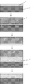
実施例1
図1に化合物半導体製造の実施例1における手順の概略を示した。
市販の直径100mm、厚さ630μmの単結晶半絶縁性GaAs元基板1上にIII族元素を含む出発原料として、トリメチルガリウム、トリエチルガリウム、トリメチルアルミニウム、トリメチルインジウム、V族元素を含む出発原料として、アルシン、ホスフィン、また伝導性制御のための不純物としてジシラン(n型制御)、トリクロロブロモメタン(p型制御)を水素ガスキャリアと共に用いた有機金属気相熱分解法により、ヘテロバイポーラトランジスタ用の化合物半導体機能層2を成長させ、化合物半導体層基板を作製した。該化合物半導体機能層2の層構造は次のような設計とした。元基板側からノンドープGaAs50nm、ノンドープAlAs50nm、ノンドープGaAs500nm、Siドープ(電子濃度3×10¹⁸/cm3)n型GaAsサブコレクタ層500nm、Siドープ(電子濃度1×1016/cm3)n型GaAsコレクタ層500nm、Cドープ(正孔濃度4×1019/cm3)p型GaAsベース層80nm、Siドープ(電子濃度3×1017/cm3)n型InGaPエミッタ層30nm、Siドープ(電子濃度3×1018/cm3)n型GaAsサブエミッタ層100nm、Siドープ(電子濃度2×1019/cm3)n型InxGa1-xAs(x=0〜0.5の傾斜構造)コンタクト層100nmである。
Example 1
FIG. 1 shows an outline of the procedure in Example 1 for manufacturing a compound semiconductor.
As a starting material containing a group III element on a commercially available single crystal semi-insulating
次に約100℃に加熱されたホットプレート上に厚さ500μm、直径100mmの透明石英製の支持基板を載せ、エレクトロンワックスを塗布溶解させた後、成長の終了した化合物半導体層基板のエピタキシャル成長面を接着面として支持基板3に接着した。このとき、化合物半導体層基板裏面から治具を介して約5kgの荷重を与え均一にエレクトロンワックスを接着剤として接着面にゆきわたらせた後、ホットプレート加熱を停止し、エレクトロンワックスを固化させ透明石英製支持基板に支持された化合物半導体層基板を得た。透明石英製の支持基板に支持された化合物半導体層基板の厚みをダイヤルゲージにより計測したところ、1130μmであった。
Next, a support substrate made of transparent quartz having a thickness of 500 μm and a diameter of 100 mm is placed on a hot plate heated to about 100 ° C., and after the electron wax is applied and dissolved, the epitaxial growth surface of the compound semiconductor layer substrate after the growth is formed. It adhered to the
次に該化合物半導体層基板の支持基板側を固定面として研磨装置に設置し、約20分間、GaAs元基板側の機械研磨を行い、約580μmを除去した。この基板を研磨装置から外し、水洗浄の後、クエン酸/過酸化水素/水系エッチング溶液に浸漬し、約4時間エッチングを実施し、GaAs元基板とエピタキシャル成長されたAlAs層より基板側のGaAs層を全て溶解した。水洗し、それから5%HF水溶液に3分間浸漬し、AlAs層を除去した。 Next, the support substrate side of the compound semiconductor layer substrate was placed in a polishing apparatus as a fixed surface, and mechanical polishing of the GaAs base substrate side was performed for about 20 minutes to remove about 580 μm. The substrate is removed from the polishing apparatus, washed with water, immersed in a citric acid / hydrogen peroxide / water etching solution, etched for about 4 hours, and the GaAs layer on the substrate side of the GaAs base substrate and the epitaxially grown AlAs layer. All were dissolved. It was washed with water and then immersed in 5% HF aqueous solution for 3 minutes to remove the AlAs layer.
次に直径100mm、厚さ約500μmの市販の単結晶Si基板4上に水素及びメタンを原料としたプラズマCVD法により厚さ約50μmの高抵抗絶縁性ダイヤモンド薄膜5を形成し鏡面研磨した基板の表面にポリイミド水溶液をスピン塗布した表面上に、上記の単結晶GaAs元基板が除去され、石英製支持基板に貼合・支持された化合物半導体層基板の研磨面を接着面として貼り合わせた後、約100℃に加熱し接着すると共に、エレクトロンワックスを溶解して支持基板を取り外した。続いて窒素雰囲気炉内において約20kgの荷重を与えながら約300℃で1時間の熱処理を行ったところ十分な接着強度を有する化合物半導体基板を得た。
Next, a high-resistance insulating diamond
この化合物半導体基板のエピタキシャル表面をアセトンにより超音波洗浄により清浄化した後、通常のリソグラフィ工程を用いてエミッタ面の寸法が100μm×100μmのヘテロバイポーラトランジスタを製作した。コレクタメタルとしてAuGe/Ni/Au、エミッタメタルおよびベースメタルとしてTi/Auを用いた。代表的なデバイス特性である電流増幅率は、コレクタ電流密度1kA/cm2・時において148であった。 After the epitaxial surface of this compound semiconductor substrate was cleaned by ultrasonic cleaning with acetone, a hetero bipolar transistor having an emitter surface dimension of 100 μm × 100 μm was fabricated using a normal lithography process. AuGe / Ni / Au was used as the collector metal, and Ti / Au was used as the emitter metal and the base metal. The current amplification factor, which is a typical device characteristic, was 148 at a collector current density of 1 kA / cm 2 · hr.
比較例1
実施例1と同様にしてエピタキシャル成長させた化合物半導体層基板を、GaAs単結晶の元基板の除去と高熱伝導基板の接着とを行うことなく、GaAs単結晶の元基板上に化合物半導体機能層をエピタキシャル成長させた化合物半導体層基板をそのまま用いてエミッタの寸法が100μm×100μmであるヘテロバイポーラトランジスタを作製し、その電流電圧特性を測定した。代表的なデバイス特性である電流増幅率は、コレクタ電流密度が1kA/cm2・時において132であった。
Comparative Example 1
A compound semiconductor layer substrate epitaxially grown in the same manner as in Example 1 is epitaxially grown on the GaAs single crystal base substrate without removing the GaAs single crystal base substrate and bonding the high thermal conductivity substrate. A heterobipolar transistor having an emitter size of 100 μm × 100 μm was produced using the compound semiconductor layer substrate as it was, and its current-voltage characteristics were measured. The current amplification factor, which is a typical device characteristic, was 132 when the collector current density was 1 kA / cm 2 · hr.
実施例2
市販の直径50mm、厚さ500μmの単結晶絶縁性サファイア製元基板(図2の6。図2は従来技術によるpn接合ダイオードを示すが、化合物半導体機能層の構造は共通なので図2において示す。)上にIII族原料としてトリメチルガリウム、トリメチルアルミニウム、V族原料としてアンモニア、また伝導性制御のための添加物としてシラン(n型制御)、ビスシクロペンタジエニルマグネシウム(p型制御)を水素ガスキャリアと共に用いた有機金属気相熱分解法により、pn接合ダイオード用化合物半導体機能層を成長させた。該化合物半導体機能層の構造は次のような設計とした。元基板側からノンドープGaNバッファー層を20nm(図2の7)、ノンドープGaNを500nm(図2の8)、Siドープ(電子濃度3×10¹⁸/cm3)n型GaNを5000nm(図2の9)、ノンドープGaNを50nm、ノンドープAlxGa1-xN(x=0.05)、Mgドープ(正孔濃度8×1018/cm3)p型GaNを80nm(図2の10)積層した構造とした。結晶成長後、該化合物半導体層基板は窒素ガス雰囲気下で約500℃、10分間熱処理し、p型GaN層の活性化を行った。
Example 2
A commercially available original substrate made of a single crystal insulating sapphire having a diameter of 50 mm and a thickness of 500 μm (6 in FIG. 2. FIG. 2 shows a pn junction diode according to the prior art, but the structure of the compound semiconductor functional layer is common and is shown in FIG. ) Hydrogen gas of trimethylgallium and trimethylaluminum as group III materials, ammonia as group V materials, silane (n-type control) and biscyclopentadienylmagnesium (p-type control) as additives for conductivity control A compound semiconductor functional layer for a pn junction diode was grown by a metal organic vapor phase pyrolysis method used together with a carrier. The structure of the compound semiconductor functional layer was designed as follows. From the original substrate side, the non-doped GaN buffer layer is 20 nm (7 in FIG. 2), the non-doped GaN is 500 nm (8 in FIG. 2), the Si-doped (
次に約100℃に加熱されたホットプレート上に厚さ500μm、直径50mmの透明石英製支持基板を載せ、エレクトロンワックスを塗布溶解させた後、成長の終了した化合物半導体層基板のエピタキシャル成長面を接着面として透明石英製基板に接着した。このときエピタキシャル基板裏面から治具を介して約5kgの荷重を与え、均一にエレクトロンワックスを接着剤として接着面にゆきわたらせた後、ホットプレート加熱を停止し、エレクトロンワックスを固化させ支持基板に支持された化合物半導体層基板を得た。得られた透明石英製支持基板付きの化合物半導体層基板の厚みをダイヤルゲージにより計測したところ1006μmであった。 Next, a support substrate made of transparent quartz having a thickness of 500 μm and a diameter of 50 mm is placed on a hot plate heated to about 100 ° C., an electron wax is applied and dissolved, and then the epitaxial growth surface of the compound semiconductor layer substrate after the growth is bonded. The surface was bonded to a transparent quartz substrate. At this time, a load of about 5 kg is applied from the back surface of the epitaxial substrate through a jig, and after uniformly spreading the electron wax on the adhesive surface as an adhesive, hot plate heating is stopped and the electron wax is solidified and supported on the support substrate. Thus obtained compound semiconductor layer substrate was obtained. The thickness of the obtained compound semiconductor layer substrate with a transparent quartz support substrate was measured with a dial gauge to be 1006 μm.
次に該貼合化合物半導合基板の、支持基板を張り合わせたエピタキシャル成長面側を固定面として研磨装置にセットし、サファイア元基板側の機械研磨を約40分間行い、約480μmを除去した。続いて研磨剤及び研磨パッドを交換し、より細かい研磨砥粒を用いて22μmを除去した。この基板を研磨装置から外し、水で洗浄した後、王水で洗浄し、約0.5μm露出したGaN面を化学研磨した後水洗乾燥し、化合物半導体層基板を得た。 Next, the epitaxial growth surface side of the bonding compound semiconductor substrate bonded to the support substrate was set as a fixed surface in a polishing apparatus, and mechanical polishing of the sapphire base substrate side was performed for about 40 minutes to remove about 480 μm. Subsequently, the abrasive and the polishing pad were replaced, and 22 μm was removed using finer abrasive grains. This substrate was removed from the polishing apparatus, washed with water, then washed with aqua regia, and the GaN surface exposed by about 0.5 μm was chemically polished and then washed with water and dried to obtain a compound semiconductor layer substrate.
次に直径50mm、厚さ約500μmの市販の単結晶Si基板(図3の12)上に水素及びメタンを原料としたプラズマCVD法により厚さ約50μmの高抵抗絶縁性ダイヤモンド薄膜(図3の11)を形成し、ダイヤモンド基板を得た。ダイヤモンド基板の表面を鏡面研磨し、その表面にポリイミド水溶液をスピン塗布し、上記の単結晶サファイア元基板を除去後に透明石英製支持基板を貼合した化合物半導体層を、その研磨面を接着面としてダイヤモンド基板と化合物半導体層を貼り合わせた後、約100℃に加熱して接着すると共に、エレクトロンワックスを溶解し、石英製支持基板を取り外した。続いて窒素雰囲気炉内において約20kgの荷重を与えながら約300℃で1時間熱処理を行ったところ、接着面の接着強度が十分な化合物半導体基板を得た。 Next, on a commercially available single crystal Si substrate (12 in FIG. 3) having a diameter of 50 mm and a thickness of about 500 μm, a high resistance insulating diamond thin film (of FIG. 3) having a thickness of about 50 μm is formed by plasma CVD using hydrogen and methane as raw materials. 11) was formed to obtain a diamond substrate. The surface of the diamond substrate is mirror-polished, a polyimide aqueous solution is spin-coated on the surface, the compound semiconductor layer bonded with a transparent quartz support substrate after removing the single crystal sapphire base substrate, and the polished surface as an adhesive surface After the diamond substrate and the compound semiconductor layer were bonded together, they were heated and bonded to about 100 ° C., the electron wax was dissolved, and the quartz support substrate was removed. Subsequently, heat treatment was performed at about 300 ° C. for 1 hour while applying a load of about 20 kg in a nitrogen atmosphere furnace, to obtain a compound semiconductor substrate having sufficient adhesion strength on the bonding surface.
次にp型GaN層表面に直径300μmのAu/Ni電極を蒸着後、400℃で5分間熱処理し、p型オーミック電極13を得た。次に、該化合物半導体基板の、p型オーミック電極の周囲をドライエッチングにより約1000nmエッチング除去した後、王水処理し、さらに50nmエッチング除去した表面にAl金属を500nm蒸着し、n型オーミック電極14とした。これによりn型GaN側に接続されたアルミニウム製n側オーミック電極とp型GaNに接合されたp側オーミック電極とを有する、メサ型のGaN/AlGaN製pnへテロ接合ダイオードを作製した。その断面構造を図3に示す。そのダイオード電流−電圧特性を試料4個につき計測したところ図4のような特性を得た。
Next, an Au / Ni electrode having a diameter of 300 μm was deposited on the surface of the p-type GaN layer and then heat-treated at 400 ° C. for 5 minutes to obtain a p-
比較例2
実施例2において製作したGaN/AlGaN化合物半導体層基板と同一の反応炉において同一の条件下で製造した同一構造の化合物半導体層基板を用いて、サファイア元基板の除去と高熱伝導基板の接着を行うことなく実施例1と同様の電極作製工程によりn型GaN側に接続されたアルミニウム製n側オーミック電極とp型GaNに接合されたp側オーミック電極とを有する、メサ型のGaN/AlGaN製pnへテロ接合ダイオードを作製した。その断面構造を図2に示す。そのダイオード電流−電圧特性を試料4個につき計測したところ図5のような特性を得た。
Comparative Example 2
Using the compound semiconductor layer substrate having the same structure manufactured under the same conditions in the same reactor as the GaN / AlGaN compound semiconductor layer substrate manufactured in Example 2, the sapphire base substrate is removed and the high thermal conductivity substrate is bonded. The mesa-type GaN / AlGaN pn having an aluminum n-side ohmic electrode connected to the n-type GaN side and a p-side ohmic electrode joined to the p-type GaN in the same electrode manufacturing process as in Example 1 A heterojunction diode was fabricated. The cross-sectional structure is shown in FIG. When the diode current-voltage characteristics were measured for four samples, the characteristics shown in FIG. 5 were obtained.
図4に示した実施例2にかかわるダイオードでは順方向バイアス側(横軸の印加電圧値>0V)で電流値が大きく、かつ逆方向バイアス側(横軸の印加電圧値<0V)でのリーク電流値が小さいのに対し、図5では順方向バイアス側で電流値が小さくなっている一方、逆方向バイアス側でのリーク電流は増加しており、全く同一の構造を有するメサ型へテロ接合ダイオードでありながら基板部をCVDダイヤモンドとSi基板に交換した化合物半導体複合基板を用いたダイオードに比べサファイア製元基板がそのまま用いられたダイオードの整流特性は十分ではないことがわかった。 In the diode of Example 2 shown in FIG. 4, the current value is large on the forward bias side (applied voltage value on the horizontal axis> 0V), and the leak is on the reverse bias side (applied voltage value on the horizontal axis <0V). While the current value is small in FIG. 5, the current value is small on the forward bias side, while the leakage current on the reverse bias side is increasing, and a mesa type heterojunction having the same structure. It was found that the rectification characteristic of the diode using the original substrate made of sapphire was not sufficient compared to the diode using the compound semiconductor composite substrate in which the substrate portion was replaced with CVD diamond and Si substrate although it was a diode.
1 単結晶半絶縁性GaAs元基板
2 エピタキシャル結晶層
3 支持用石英基板
4 Si基板
5 プラズマCVD法ダイヤモンド層
6 単結晶サファイア元基板
7 ノンドープGaNバッファー層
8 ノンドープGaNエピタキシャル層
9 Siドープn型GaNエピタキシャル層
10 Mgドープp型GaNエピタキシャル層
11 プラズマCVD法ダイヤモンド層
12 Si基板
13 オーミックp電極
14 オーミックn電極
DESCRIPTION OF
Claims (5)
(ア)元基板上に化合物半導体機能層をエピタキシャル成長させて得られた化合物半導体層基板のエピタキシャル成長面に支持基板を仮接着する工程。
(イ)該元基板の全部および該元基板近傍の該化合物半導体機能層の一部を研磨により除去する工程。
(ウ)該化合物半導体層基板の工程(イ)により露出した化合物半導体機能層に、熱伝導度が該元基板より大きい物質からなる高熱伝導基板を接着する工程。
(エ)エピタキシャル成長面に仮接着された該支持基板を分離除去する工程。 The manufacturing method of the compound semiconductor substrate characterized by including the following processes.
(A) A step of temporarily adhering a support substrate to an epitaxial growth surface of a compound semiconductor layer substrate obtained by epitaxially growing a compound semiconductor functional layer on an original substrate.
(A) A step of removing all of the original substrate and a part of the compound semiconductor functional layer in the vicinity of the original substrate by polishing.
(C) A step of bonding a high thermal conductivity substrate made of a material having a thermal conductivity larger than that of the original substrate to the compound semiconductor functional layer exposed in the step (a) of the compound semiconductor layer substrate.
(D) A step of separating and removing the support substrate temporarily bonded to the epitaxial growth surface.
(カ)元基板上に化合物半導体機能層をエピタキシャル成長させて得られた化合物半導体層基板のエピタキシャル成長面に、熱伝導度が該元基板より大きい物質からなる高熱伝導基板を接着する工程。
(キ)該元基板の全部および該元基板近傍の該化合物半導体機能層の一部を研磨により除去する工程。 The manufacturing method of the compound semiconductor substrate characterized by including the following processes.
(F) A step of bonding a high thermal conductivity substrate made of a material having a thermal conductivity larger than that of the original substrate to an epitaxial growth surface of the compound semiconductor layer substrate obtained by epitaxially growing the compound semiconductor functional layer on the original substrate.
(G) A step of removing all of the original substrate and a part of the compound semiconductor functional layer in the vicinity of the original substrate by polishing.
An electronic device manufacturing method using the compound semiconductor substrate manufactured by the manufacturing method according to claim 1.
Priority Applications (8)
| Application Number | Priority Date | Filing Date | Title |
|---|---|---|---|
| JP2003365736A JP2005129825A (en) | 2003-10-27 | 2003-10-27 | Manufacturing method of compound semiconductor substrate |
| TW093132261A TW200520212A (en) | 2003-10-27 | 2004-10-22 | Method for manufacturing compound semiconductor substrate |
| PCT/JP2004/016186 WO2005041287A1 (en) | 2003-10-27 | 2004-10-25 | Method for manufacturing compound semiconductor substrate |
| KR1020067010033A KR20060101499A (en) | 2003-10-27 | 2004-10-25 | Method for manufacturing compound semiconductor substrate |
| DE112004002033T DE112004002033T5 (en) | 2003-10-27 | 2004-10-25 | A method for producing a compound semiconductor substrate |
| US10/577,069 US20070082467A1 (en) | 2003-10-27 | 2004-10-25 | Method for manufacturing compound semiconductor substrate |
| GB0609682A GB2422489B8 (en) | 2003-10-27 | 2004-10-25 | Method for manufacturing compound semiconductor substrate |
| CN2004800313161A CN1871699B (en) | 2003-10-27 | 2004-10-25 | Method for manufacturing compound semiconductor substrate |
Applications Claiming Priority (1)
| Application Number | Priority Date | Filing Date | Title |
|---|---|---|---|
| JP2003365736A JP2005129825A (en) | 2003-10-27 | 2003-10-27 | Manufacturing method of compound semiconductor substrate |
Publications (2)
| Publication Number | Publication Date |
|---|---|
| JP2005129825A true JP2005129825A (en) | 2005-05-19 |
| JP2005129825A5 JP2005129825A5 (en) | 2006-11-02 |
Family
ID=34510191
Family Applications (1)
| Application Number | Title | Priority Date | Filing Date |
|---|---|---|---|
| JP2003365736A Pending JP2005129825A (en) | 2003-10-27 | 2003-10-27 | Manufacturing method of compound semiconductor substrate |
Country Status (8)
| Country | Link |
|---|---|
| US (1) | US20070082467A1 (en) |
| JP (1) | JP2005129825A (en) |
| KR (1) | KR20060101499A (en) |
| CN (1) | CN1871699B (en) |
| DE (1) | DE112004002033T5 (en) |
| GB (1) | GB2422489B8 (en) |
| TW (1) | TW200520212A (en) |
| WO (1) | WO2005041287A1 (en) |
Cited By (8)
| Publication number | Priority date | Publication date | Assignee | Title |
|---|---|---|---|---|
| JP2010087360A (en) * | 2008-10-01 | 2010-04-15 | Kyoto Institute Of Technology | Production process of semiconductor substrate, and semiconductor substrate |
| JP2013191655A (en) * | 2012-03-13 | 2013-09-26 | Nippon Telegr & Teleph Corp <Ntt> | Heterojunction bipolar transistor and manufacturing method of the same |
| JP2015056602A (en) * | 2013-09-13 | 2015-03-23 | 日本電信電話株式会社 | Semiconductor device and manufacturing method of the same |
| JP2016197737A (en) * | 2016-06-29 | 2016-11-24 | 株式会社タムラ製作所 | Semiconductor device and method for manufacturing the same, and crystal laminate structure |
| US10230007B2 (en) | 2014-07-25 | 2019-03-12 | Tamura Corporation | Semiconductor element, method for manufacturing same, semiconductor substrate, and crystal laminate structure |
| JP2019096716A (en) * | 2017-11-22 | 2019-06-20 | 日本電信電話株式会社 | Semiconductor wafer and method of manufacturing the same, and heterojunction bipolar transistor and method of manufacturing the same |
| KR20200026822A (en) * | 2017-07-14 | 2020-03-11 | 신에쓰 가가꾸 고교 가부시끼가이샤 | High thermal conductivity device substrate and manufacturing method thereof |
| WO2021210047A1 (en) | 2020-04-13 | 2021-10-21 | 三菱電機株式会社 | Method for manufacturing semiconductor element |
Families Citing this family (8)
| Publication number | Priority date | Publication date | Assignee | Title |
|---|---|---|---|---|
| US20060284167A1 (en) * | 2005-06-17 | 2006-12-21 | Godfrey Augustine | Multilayered substrate obtained via wafer bonding for power applications |
| US7799599B1 (en) * | 2007-05-31 | 2010-09-21 | Chien-Min Sung | Single crystal silicon carbide layers on diamond and associated methods |
| JP2009143756A (en) * | 2007-12-13 | 2009-07-02 | Shin Etsu Chem Co Ltd | MULTILAYER SUBSTRATE INCLUDING GaN LAYER, ITS MANUFACTURING METHOD AND DEVICE |
| JP5906001B2 (en) * | 2009-03-10 | 2016-04-20 | 昭和電工株式会社 | Epitaxial wafer for light emitting diode |
| WO2011005444A1 (en) * | 2009-06-22 | 2011-01-13 | Raytheon Company | Gallium nitride for liquid crystal electrodes |
| JP5684501B2 (en) | 2010-07-06 | 2015-03-11 | 昭和電工株式会社 | Epitaxial wafer for light emitting diode |
| KR102143440B1 (en) | 2017-01-20 | 2020-08-11 | 한양대학교 산학협력단 | 3d neuromorphic device and method of manufacturing the same |
| GB202018616D0 (en) * | 2020-11-26 | 2021-01-13 | Element Six Tech Ltd | A diamond assembly |
Citations (5)
| Publication number | Priority date | Publication date | Assignee | Title |
|---|---|---|---|---|
| JPH06349731A (en) * | 1993-06-03 | 1994-12-22 | Nec Corp | Manufacture of hybrid semiconductor-laminated structure |
| JPH07193294A (en) * | 1993-11-01 | 1995-07-28 | Matsushita Electric Ind Co Ltd | Electronic component and its manufacture |
| JPH07226491A (en) * | 1994-01-31 | 1995-08-22 | Philips Electron Nv | Preparation of electronic device |
| JPH11103125A (en) * | 1997-09-29 | 1999-04-13 | Furukawa Electric Co Ltd:The | Manufacture of surface emitting semiconductor laser device |
| JP2002542622A (en) * | 1999-04-21 | 2002-12-10 | シリコン ジェネシス コーポレイション | Surface finishing of SOI substrate using epi process |
Family Cites Families (8)
| Publication number | Priority date | Publication date | Assignee | Title |
|---|---|---|---|---|
| US4040849A (en) * | 1976-01-06 | 1977-08-09 | General Electric Company | Polycrystalline silicon articles by sintering |
| JP2669368B2 (en) * | 1994-03-16 | 1997-10-27 | 日本電気株式会社 | Method for manufacturing compound semiconductor laminated structure on Si substrate |
| US6984571B1 (en) * | 1999-10-01 | 2006-01-10 | Ziptronix, Inc. | Three dimensional device integration method and integrated device |
| US6562648B1 (en) * | 2000-08-23 | 2003-05-13 | Xerox Corporation | Structure and method for separation and transfer of semiconductor thin films onto dissimilar substrate materials |
| EP2262007B1 (en) * | 2002-01-28 | 2016-11-23 | Nichia Corporation | Nitride semiconductor element with supporting substrate |
| US6830813B2 (en) * | 2003-03-27 | 2004-12-14 | Intel Corporation | Stress-reducing structure for electronic devices |
| US7407863B2 (en) * | 2003-10-07 | 2008-08-05 | Board Of Trustees Of The University Of Illinois | Adhesive bonding with low temperature grown amorphous or polycrystalline compound semiconductors |
| US7547925B2 (en) * | 2005-11-14 | 2009-06-16 | Palo Alto Research Center Incorporated | Superlattice strain relief layer for semiconductor devices |
-
2003
- 2003-10-27 JP JP2003365736A patent/JP2005129825A/en active Pending
-
2004
- 2004-10-22 TW TW093132261A patent/TW200520212A/en unknown
- 2004-10-25 CN CN2004800313161A patent/CN1871699B/en not_active Expired - Fee Related
- 2004-10-25 GB GB0609682A patent/GB2422489B8/en not_active Expired - Fee Related
- 2004-10-25 US US10/577,069 patent/US20070082467A1/en not_active Abandoned
- 2004-10-25 WO PCT/JP2004/016186 patent/WO2005041287A1/en active Application Filing
- 2004-10-25 KR KR1020067010033A patent/KR20060101499A/en active Search and Examination
- 2004-10-25 DE DE112004002033T patent/DE112004002033T5/en not_active Withdrawn
Patent Citations (5)
| Publication number | Priority date | Publication date | Assignee | Title |
|---|---|---|---|---|
| JPH06349731A (en) * | 1993-06-03 | 1994-12-22 | Nec Corp | Manufacture of hybrid semiconductor-laminated structure |
| JPH07193294A (en) * | 1993-11-01 | 1995-07-28 | Matsushita Electric Ind Co Ltd | Electronic component and its manufacture |
| JPH07226491A (en) * | 1994-01-31 | 1995-08-22 | Philips Electron Nv | Preparation of electronic device |
| JPH11103125A (en) * | 1997-09-29 | 1999-04-13 | Furukawa Electric Co Ltd:The | Manufacture of surface emitting semiconductor laser device |
| JP2002542622A (en) * | 1999-04-21 | 2002-12-10 | シリコン ジェネシス コーポレイション | Surface finishing of SOI substrate using epi process |
Cited By (12)
| Publication number | Priority date | Publication date | Assignee | Title |
|---|---|---|---|---|
| JP2010087360A (en) * | 2008-10-01 | 2010-04-15 | Kyoto Institute Of Technology | Production process of semiconductor substrate, and semiconductor substrate |
| JP2013191655A (en) * | 2012-03-13 | 2013-09-26 | Nippon Telegr & Teleph Corp <Ntt> | Heterojunction bipolar transistor and manufacturing method of the same |
| JP2015056602A (en) * | 2013-09-13 | 2015-03-23 | 日本電信電話株式会社 | Semiconductor device and manufacturing method of the same |
| US10230007B2 (en) | 2014-07-25 | 2019-03-12 | Tamura Corporation | Semiconductor element, method for manufacturing same, semiconductor substrate, and crystal laminate structure |
| JP2016197737A (en) * | 2016-06-29 | 2016-11-24 | 株式会社タムラ製作所 | Semiconductor device and method for manufacturing the same, and crystal laminate structure |
| KR20200026822A (en) * | 2017-07-14 | 2020-03-11 | 신에쓰 가가꾸 고교 가부시끼가이샤 | High thermal conductivity device substrate and manufacturing method thereof |
| CN110892506A (en) * | 2017-07-14 | 2020-03-17 | 信越化学工业株式会社 | Device substrate having high thermal conductivity and method of manufacturing the same |
| KR102558905B1 (en) * | 2017-07-14 | 2023-07-21 | 신에쓰 가가꾸 고교 가부시끼가이샤 | High thermal conductivity device substrate and manufacturing method thereof |
| CN110892506B (en) * | 2017-07-14 | 2024-04-09 | 信越化学工业株式会社 | Device substrate having high thermal conductivity and method of manufacturing the same |
| JP2019096716A (en) * | 2017-11-22 | 2019-06-20 | 日本電信電話株式会社 | Semiconductor wafer and method of manufacturing the same, and heterojunction bipolar transistor and method of manufacturing the same |
| WO2021210047A1 (en) | 2020-04-13 | 2021-10-21 | 三菱電機株式会社 | Method for manufacturing semiconductor element |
| KR20220143741A (en) | 2020-04-13 | 2022-10-25 | 미쓰비시덴키 가부시키가이샤 | Method of manufacturing semiconductor device |
Also Published As
| Publication number | Publication date |
|---|---|
| GB2422489B8 (en) | 2007-03-30 |
| GB2422489B (en) | 2007-03-14 |
| CN1871699B (en) | 2012-06-27 |
| WO2005041287A1 (en) | 2005-05-06 |
| GB2422489A (en) | 2006-07-26 |
| TW200520212A (en) | 2005-06-16 |
| CN1871699A (en) | 2006-11-29 |
| GB0609682D0 (en) | 2006-06-28 |
| US20070082467A1 (en) | 2007-04-12 |
| DE112004002033T5 (en) | 2006-09-21 |
| KR20060101499A (en) | 2006-09-25 |
Similar Documents
| Publication | Publication Date | Title |
|---|---|---|
| JP4095066B2 (en) | Semiconductor structure of gallium nitride based semiconductor | |
| JP3946427B2 (en) | Epitaxial growth substrate manufacturing method and semiconductor device manufacturing method using this epitaxial growth substrate | |
| JP2005129825A (en) | Manufacturing method of compound semiconductor substrate | |
| JP4917152B2 (en) | Group III-nitride formation on Ge | |
| JP5978548B2 (en) | Method for manufacturing gallium nitride type wafer on diamond | |
| JP3914615B2 (en) | Semiconductor light emitting device and manufacturing method thereof | |
| WO2011033776A1 (en) | Method for producing compound semiconductor crystal, method for manufacturing electronic device, and semiconductor substrate | |
| WO2022070699A1 (en) | Epitaxial wafer for ultraviolet light emitting elements, method for producing metal bonded susbtrate for ultraviolet light emitting elements, method for producing ultraviolet light emitting element, and method for producing ultraviolet light emitting element array | |
| US20060124956A1 (en) | Quasi group III-nitride substrates and methods of mass production of the same | |
| US8395184B2 (en) | Semiconductor device based on the cubic silicon carbide single crystal thin film | |
| US8709950B2 (en) | Silicon carbide substrate, epitaxial wafer and manufacturing method of silicon carbide substrate | |
| KR20120063716A (en) | Fabricating method of semiconductor device for reuse of substrate | |
| KR101105918B1 (en) | Method of manufacturing nitride compound semiconductor device | |
| JP2009190918A (en) | Method for manufacturing nitride semiconductor substrate and method for manufacturing nitride semiconductor device | |
| CN113871473A (en) | Device and method for controlling van der Waals epitaxy and remote epitaxy growth modes | |
| CN106505095B (en) | Composite substrate, preparation method thereof and epitaxial wafer | |
| JP6818964B1 (en) | Composite substrate, manufacturing method of composite substrate, semiconductor device and manufacturing method of semiconductor device | |
| KR100638351B1 (en) | semiconductor substrate and the manufacturing method of the same | |
| JP6810017B2 (en) | Manufacturing method of semiconductor wafer, manufacturing method of heterojunction bipolar transistor | |
| US11087974B2 (en) | Preparation of compound semiconductor substrate for epitaxial growth via non-destructive epitaxial lift-off | |
| KR100813561B1 (en) | semiconductor substrate and the manufacturing method of the same | |
| TW202316494A (en) | Provisionally bonded wafer and method for producing same | |
| JPH10106949A (en) | Gallium nitride semiconductor substrate and its manufacture | |
| KR100770583B1 (en) | The Light Emitting Device using the Free-Standing Semiconductor Substrate and Manufacturing of the same | |
| JPS61183918A (en) | Manufacture of semiconductor device |
Legal Events
| Date | Code | Title | Description |
|---|---|---|---|
| A521 | Written amendment |
Free format text: JAPANESE INTERMEDIATE CODE: A523 Effective date: 20060913 |
|
| A621 | Written request for application examination |
Free format text: JAPANESE INTERMEDIATE CODE: A621 Effective date: 20060913 |
|
| RD05 | Notification of revocation of power of attorney |
Free format text: JAPANESE INTERMEDIATE CODE: A7425 Effective date: 20080130 |
|
| RD05 | Notification of revocation of power of attorney |
Free format text: JAPANESE INTERMEDIATE CODE: A7425 Effective date: 20080513 |
|
| A131 | Notification of reasons for refusal |
Free format text: JAPANESE INTERMEDIATE CODE: A131 Effective date: 20101130 |
|
| A521 | Written amendment |
Free format text: JAPANESE INTERMEDIATE CODE: A523 Effective date: 20110131 |
|
| A131 | Notification of reasons for refusal |
Free format text: JAPANESE INTERMEDIATE CODE: A131 Effective date: 20110412 |
|
| A02 | Decision of refusal |
Free format text: JAPANESE INTERMEDIATE CODE: A02 Effective date: 20110823 |