JP2005093712A - Semiconductor light emitting device - Google Patents
Semiconductor light emitting device Download PDFInfo
- Publication number
- JP2005093712A JP2005093712A JP2003324884A JP2003324884A JP2005093712A JP 2005093712 A JP2005093712 A JP 2005093712A JP 2003324884 A JP2003324884 A JP 2003324884A JP 2003324884 A JP2003324884 A JP 2003324884A JP 2005093712 A JP2005093712 A JP 2005093712A
- Authority
- JP
- Japan
- Prior art keywords
- light
- phosphor
- light emitting
- led chip
- emitting device
- Prior art date
- Legal status (The legal status is an assumption and is not a legal conclusion. Google has not performed a legal analysis and makes no representation as to the accuracy of the status listed.)
- Pending
Links
- 239000004065 semiconductor Substances 0.000 title claims abstract description 20
- 238000006243 chemical reaction Methods 0.000 claims abstract description 32
- 229920005989 resin Polymers 0.000 claims abstract description 28
- 239000011347 resin Substances 0.000 claims abstract description 28
- OAICVXFJPJFONN-UHFFFAOYSA-N Phosphorus Chemical compound [P] OAICVXFJPJFONN-UHFFFAOYSA-N 0.000 claims description 54
- 239000003795 chemical substances by application Substances 0.000 claims description 39
- 229910052761 rare earth metal Inorganic materials 0.000 claims description 8
- 150000002910 rare earth metals Chemical class 0.000 claims description 7
- 239000004925 Acrylic resin Substances 0.000 claims description 3
- 229920000178 Acrylic resin Polymers 0.000 claims description 3
- 150000004645 aluminates Chemical class 0.000 claims description 3
- 150000001925 cycloalkenes Chemical class 0.000 claims description 3
- 239000003822 epoxy resin Substances 0.000 claims description 3
- 229920000647 polyepoxide Polymers 0.000 claims description 3
- 229920002050 silicone resin Polymers 0.000 claims description 3
- -1 rare earth activated orthosilicate Chemical class 0.000 claims 1
- 239000000758 substrate Substances 0.000 abstract description 3
- 239000002270 dispersing agent Substances 0.000 abstract 1
- 239000000654 additive Substances 0.000 description 5
- 230000000996 additive effect Effects 0.000 description 5
- 230000007423 decrease Effects 0.000 description 3
- 230000000694 effects Effects 0.000 description 3
- 238000000034 method Methods 0.000 description 3
- 239000000203 mixture Substances 0.000 description 3
- 230000003287 optical effect Effects 0.000 description 3
- 238000007789 sealing Methods 0.000 description 3
- VYPSYNLAJGMNEJ-UHFFFAOYSA-N Silicium dioxide Chemical compound O=[Si]=O VYPSYNLAJGMNEJ-UHFFFAOYSA-N 0.000 description 2
- 239000003086 colorant Substances 0.000 description 2
- 230000006866 deterioration Effects 0.000 description 2
- BPQQTUXANYXVAA-UHFFFAOYSA-N Orthosilicate Chemical compound [O-][Si]([O-])([O-])[O-] BPQQTUXANYXVAA-UHFFFAOYSA-N 0.000 description 1
- GWEVSGVZZGPLCZ-UHFFFAOYSA-N Titan oxide Chemical group O=[Ti]=O GWEVSGVZZGPLCZ-UHFFFAOYSA-N 0.000 description 1
- XAGFODPZIPBFFR-UHFFFAOYSA-N aluminium Chemical compound [Al] XAGFODPZIPBFFR-UHFFFAOYSA-N 0.000 description 1
- 229910052782 aluminium Inorganic materials 0.000 description 1
- PNEYBMLMFCGWSK-UHFFFAOYSA-N aluminium oxide Inorganic materials [O-2].[O-2].[O-2].[Al+3].[Al+3] PNEYBMLMFCGWSK-UHFFFAOYSA-N 0.000 description 1
- 230000000295 complement effect Effects 0.000 description 1
- 238000010586 diagram Methods 0.000 description 1
- 238000009792 diffusion process Methods 0.000 description 1
- 230000006355 external stress Effects 0.000 description 1
- 238000012423 maintenance Methods 0.000 description 1
- 238000004519 manufacturing process Methods 0.000 description 1
- 229910052605 nesosilicate Inorganic materials 0.000 description 1
- 150000004762 orthosilicates Chemical class 0.000 description 1
- 238000010422 painting Methods 0.000 description 1
- 238000002310 reflectometry Methods 0.000 description 1
- 150000003839 salts Chemical class 0.000 description 1
- 239000000377 silicon dioxide Substances 0.000 description 1
- 229910052709 silver Inorganic materials 0.000 description 1
- 239000004332 silver Substances 0.000 description 1
- 229910000679 solder Inorganic materials 0.000 description 1
- 230000003595 spectral effect Effects 0.000 description 1
- 230000035882 stress Effects 0.000 description 1
- 239000000126 substance Substances 0.000 description 1
- OGIDPMRJRNCKJF-UHFFFAOYSA-N titanium oxide Inorganic materials [Ti]=O OGIDPMRJRNCKJF-UHFFFAOYSA-N 0.000 description 1
- 238000007740 vapor deposition Methods 0.000 description 1
Images


Classifications
-
- H—ELECTRICITY
- H01—ELECTRIC ELEMENTS
- H01L—SEMICONDUCTOR DEVICES NOT COVERED BY CLASS H10
- H01L33/00—Semiconductor devices having potential barriers specially adapted for light emission; Processes or apparatus specially adapted for the manufacture or treatment thereof or of parts thereof; Details thereof
- H01L33/48—Semiconductor devices having potential barriers specially adapted for light emission; Processes or apparatus specially adapted for the manufacture or treatment thereof or of parts thereof; Details thereof characterised by the semiconductor body packages
- H01L33/52—Encapsulations
- H01L33/56—Materials, e.g. epoxy or silicone resin
-
- H—ELECTRICITY
- H01—ELECTRIC ELEMENTS
- H01L—SEMICONDUCTOR DEVICES NOT COVERED BY CLASS H10
- H01L2224/00—Indexing scheme for arrangements for connecting or disconnecting semiconductor or solid-state bodies and methods related thereto as covered by H01L24/00
- H01L2224/01—Means for bonding being attached to, or being formed on, the surface to be connected, e.g. chip-to-package, die-attach, "first-level" interconnects; Manufacturing methods related thereto
- H01L2224/42—Wire connectors; Manufacturing methods related thereto
- H01L2224/47—Structure, shape, material or disposition of the wire connectors after the connecting process
- H01L2224/48—Structure, shape, material or disposition of the wire connectors after the connecting process of an individual wire connector
- H01L2224/4805—Shape
- H01L2224/4809—Loop shape
- H01L2224/48091—Arched
-
- H—ELECTRICITY
- H01—ELECTRIC ELEMENTS
- H01L—SEMICONDUCTOR DEVICES NOT COVERED BY CLASS H10
- H01L2224/00—Indexing scheme for arrangements for connecting or disconnecting semiconductor or solid-state bodies and methods related thereto as covered by H01L24/00
- H01L2224/01—Means for bonding being attached to, or being formed on, the surface to be connected, e.g. chip-to-package, die-attach, "first-level" interconnects; Manufacturing methods related thereto
- H01L2224/42—Wire connectors; Manufacturing methods related thereto
- H01L2224/47—Structure, shape, material or disposition of the wire connectors after the connecting process
- H01L2224/48—Structure, shape, material or disposition of the wire connectors after the connecting process of an individual wire connector
- H01L2224/481—Disposition
- H01L2224/48151—Connecting between a semiconductor or solid-state body and an item not being a semiconductor or solid-state body, e.g. chip-to-substrate, chip-to-passive
- H01L2224/48221—Connecting between a semiconductor or solid-state body and an item not being a semiconductor or solid-state body, e.g. chip-to-substrate, chip-to-passive the body and the item being stacked
- H01L2224/48245—Connecting between a semiconductor or solid-state body and an item not being a semiconductor or solid-state body, e.g. chip-to-substrate, chip-to-passive the body and the item being stacked the item being metallic
- H01L2224/48247—Connecting between a semiconductor or solid-state body and an item not being a semiconductor or solid-state body, e.g. chip-to-substrate, chip-to-passive the body and the item being stacked the item being metallic connecting the wire to a bond pad of the item
-
- H—ELECTRICITY
- H01—ELECTRIC ELEMENTS
- H01L—SEMICONDUCTOR DEVICES NOT COVERED BY CLASS H10
- H01L2224/00—Indexing scheme for arrangements for connecting or disconnecting semiconductor or solid-state bodies and methods related thereto as covered by H01L24/00
- H01L2224/01—Means for bonding being attached to, or being formed on, the surface to be connected, e.g. chip-to-package, die-attach, "first-level" interconnects; Manufacturing methods related thereto
- H01L2224/42—Wire connectors; Manufacturing methods related thereto
- H01L2224/47—Structure, shape, material or disposition of the wire connectors after the connecting process
- H01L2224/48—Structure, shape, material or disposition of the wire connectors after the connecting process of an individual wire connector
- H01L2224/481—Disposition
- H01L2224/48151—Connecting between a semiconductor or solid-state body and an item not being a semiconductor or solid-state body, e.g. chip-to-substrate, chip-to-passive
- H01L2224/48221—Connecting between a semiconductor or solid-state body and an item not being a semiconductor or solid-state body, e.g. chip-to-substrate, chip-to-passive the body and the item being stacked
- H01L2224/48245—Connecting between a semiconductor or solid-state body and an item not being a semiconductor or solid-state body, e.g. chip-to-substrate, chip-to-passive the body and the item being stacked the item being metallic
- H01L2224/48257—Connecting between a semiconductor or solid-state body and an item not being a semiconductor or solid-state body, e.g. chip-to-substrate, chip-to-passive the body and the item being stacked the item being metallic connecting the wire to a die pad of the item
-
- H—ELECTRICITY
- H01—ELECTRIC ELEMENTS
- H01L—SEMICONDUCTOR DEVICES NOT COVERED BY CLASS H10
- H01L2224/00—Indexing scheme for arrangements for connecting or disconnecting semiconductor or solid-state bodies and methods related thereto as covered by H01L24/00
- H01L2224/80—Methods for connecting semiconductor or other solid state bodies using means for bonding being attached to, or being formed on, the surface to be connected
- H01L2224/85—Methods for connecting semiconductor or other solid state bodies using means for bonding being attached to, or being formed on, the surface to be connected using a wire connector
- H01L2224/85909—Post-treatment of the connector or wire bonding area
- H01L2224/8592—Applying permanent coating, e.g. protective coating
-
- H—ELECTRICITY
- H01—ELECTRIC ELEMENTS
- H01L—SEMICONDUCTOR DEVICES NOT COVERED BY CLASS H10
- H01L2924/00—Indexing scheme for arrangements or methods for connecting or disconnecting semiconductor or solid-state bodies as covered by H01L24/00
- H01L2924/15—Details of package parts other than the semiconductor or other solid state devices to be connected
- H01L2924/181—Encapsulation
-
- H—ELECTRICITY
- H01—ELECTRIC ELEMENTS
- H01L—SEMICONDUCTOR DEVICES NOT COVERED BY CLASS H10
- H01L2933/00—Details relating to devices covered by the group H01L33/00 but not provided for in its subgroups
- H01L2933/0091—Scattering means in or on the semiconductor body or semiconductor body package
Landscapes
- Engineering & Computer Science (AREA)
- Microelectronics & Electronic Packaging (AREA)
- Manufacturing & Machinery (AREA)
- Computer Hardware Design (AREA)
- Power Engineering (AREA)
- Led Device Packages (AREA)
Abstract
Description
本発明は、半導体発光装置に関するものであり、詳しくは半導体発光素子(発光ダイオードチップ)から出射した光と、発光ダイオードチップから出射して蛍光体によって波長変換された光との組み合わせの加法混色によって任意の色調の光を発する半導体発光装置に関する。 The present invention relates to a semiconductor light emitting device, and more specifically, by additive color mixing of a combination of light emitted from a semiconductor light emitting element (light emitting diode chip) and light emitted from the light emitting diode chip and wavelength-converted by a phosphor. The present invention relates to a semiconductor light emitting device that emits light of an arbitrary color tone.
急峻なスペクトル分布特性を持った光を発する発光ダイオード(LED)チップを光源にして白色光を放出するLEDを実現するためには、LEDチップから出射された光と、LEDチップから出射された光が蛍光体を励起して波長変換された光との加法混色によって可能になる。例えば、LEDチップから出射される光が青色光の場合には、青色光に励起されて青色の補色となる黄色光に波長変換する蛍光体を用いることにより、LEDチップから出射された青色光が蛍光体を励起することによって波長変換された黄色光と、LEDチップから出射された青色光との加法混色によって白色光を作り出すことができる。また、LEDチップから出射される光が青色光であっても、青色光に励起されて緑色光および赤色光にそれぞれ波長変換する2種類の蛍光体を混合したものを用いることにより、LEDチップから出射された青色光が蛍光体を励起することによって波長変換された緑色光および赤色光と、LEDチップから出射された青色光との加法混色によって白色光を作り出すこともできる。また、LEDチップから出射される光が紫外光の場合には、紫外光に励起されて青色光、緑色光および赤色光にそれぞれ波長変換する3種類の蛍光体を混合したものを用いることにより、LEDチップから出射された紫外光が蛍光体を励起することによって波長変換された青色光、緑色光および赤色光の加法混色によって白色光を作り出すこともできる。さらに、LEDチップから出射される光の発光色と蛍光体とを適宜組み合わせることによって白色光以外の種々な発光色を作り出すことができる。 In order to realize an LED that emits white light using a light emitting diode (LED) chip that emits light having a steep spectral distribution characteristic as a light source, light emitted from the LED chip and light emitted from the LED chip are used. Is enabled by additive color mixing with the light whose wavelength has been converted by exciting the phosphor. For example, when the light emitted from the LED chip is blue light, the blue light emitted from the LED chip can be obtained by using a phosphor that is excited by the blue light and converts the wavelength to yellow light that is a complementary color of blue. White light can be produced by additive color mixture of yellow light wavelength-converted by exciting the phosphor and blue light emitted from the LED chip. Moreover, even if the light emitted from the LED chip is blue light, by using a mixture of two kinds of phosphors that are excited by blue light and respectively convert the wavelength into green light and red light, White light can also be created by additive color mixing of green light and red light, which have been wavelength-converted by the emitted blue light exciting the phosphor, and the blue light emitted from the LED chip. In addition, when the light emitted from the LED chip is ultraviolet light, by using a mixture of three kinds of phosphors that are excited by ultraviolet light and convert the wavelength into blue light, green light, and red light, respectively, White light can also be created by additive color mixing of blue light, green light, and red light, whose wavelengths are converted by exciting the phosphor with ultraviolet light emitted from the LED chip. Furthermore, various emission colors other than white light can be created by appropriately combining the emission color of the light emitted from the LED chip and the phosphor.
このように、光源から出射された光で蛍光体を励起して波長変換し、光源から出射された光とは異なる色調の光を放出するようなLEDにおいては、蛍光体は光透過性樹脂に混入させて使用されるのが一般的であるが、蛍光体と共に拡散剤を混入したものがある。例えば、一対のリードフレームの一方の端部に載設されたLEDチップを、光透過性樹脂に蛍光体と5〜20wt%の拡散剤とを混入した波長変換部材で封止した構成のLEDランプである。 In this way, in an LED that excites the phosphor with the light emitted from the light source, converts the wavelength, and emits light having a color tone different from the light emitted from the light source, the phosphor becomes a light-transmitting resin. Generally, it is used by mixing it, but there is one in which a diffusing agent is mixed together with a phosphor. For example, an LED lamp having a configuration in which an LED chip mounted on one end of a pair of lead frames is sealed with a wavelength conversion member in which a phosphor and 5 to 20 wt% diffusing agent are mixed in a light-transmitting resin. It is.
LEDチップを光透過性樹脂に蛍光体を混入した波長変換部材で封止した構造のLEDにおいては、蛍光体が有機蛍光体の場合、蛍光体がLEDチップから出射される光および太陽光などの外光に含まれる、紫外光や可視光を受けて時間経過と共に劣化し、LEDから放出される光の色調がシフトしたり、光量が低下するなどの問題を生じる。 In an LED having a structure in which an LED chip is sealed with a wavelength conversion member in which a phosphor is mixed in a light-transmitting resin, when the phosphor is an organic phosphor, the phosphor emits light emitted from the LED chip, sunlight, or the like. When the ultraviolet light or visible light contained in the external light is received, the light deteriorates with time, and the color tone of the light emitted from the LED shifts or the light quantity decreases.
このような問題を解消するために、光透過性樹脂に蛍光体と共に拡散剤を混入した波長変換部材でLEDチップを封止することによって、波長変換部材に入射した光を蛍光体に向かう光と拡散剤に向かう光とに分岐させ、蛍光体に向かう光の割合を減少させると同時に、拡散剤によって散乱された光度の低い光が蛍光体に向かうようにした。その結果、蛍光剤の劣化の進行が低減されることで、LEDから放出される光の色調のシフトおよび光度維持率の改善を図ったものである(例えば、特許文献1参照。)。
しかしながら、上述した従来のLEDは、蛍光体の劣化を低減してLEDから放出される光の色調および光量の経時変化を低減させるのが主な目的であるため、光量の確保(高輝度化)および色調のバラツキ低減に対する施策については不十分なところがあった。 However, the above-described conventional LED is mainly intended to reduce deterioration of the phosphor and change the color tone and light amount of the light emitted from the LED over time, so that the light amount is ensured (high brightness). In addition, there were insufficient measures to reduce color variation.
そこで、本発明は上記問題に鑑みて創案なされたもので、高輝度で色調バラツキが少なく、高信頼性の光源となるような発光ダイオードを提供するものである。 Accordingly, the present invention has been made in view of the above problems, and provides a light-emitting diode that is a high-reliability light source with high brightness and little color variation.
上記課題を解決するために、本発明の請求項1に記載された発明は、少なくとも一つの発光ダイオードチップを、光透過性樹脂に少なくとも1種類の蛍光体と拡散剤とを混入した波長変換部材で封止した発光ダイオードであって、前記波長変換部材には20〜80wt%の前記拡散剤が混入されていることを特徴とするものである。
In order to solve the above-mentioned problem, the invention described in
また、本発明の請求項2に記載された発明は、請求項1において、前記発光ダイオードチップは、紫外光を発光することを特徴とするものである。
The invention described in
また、本発明の請求項3に記載された発明は、請求項1において、前記発光ダイオードチップは、青色光または緑色光を発光することを特徴とするものである。
The invention described in
また、本発明の請求項4に記載された発明は、請求項1において、前記発光ダイオードチップは、青色光を発光る発光ダイオードチップと緑色光を発光する発光ダイオードチップとで構成されていることを特徴とするものである。 According to a fourth aspect of the present invention, in the first aspect, the light emitting diode chip comprises a light emitting diode chip that emits blue light and a light emitting diode chip that emits green light. It is characterized by.
また、本発明の請求項5に記載された発明は、請求項1から4の何れか1項において、前記蛍光体は、希土類を付活したアルミン酸塩、希土類を付活したチオ没食子酸塩および希土類を付活したオルトケイ酸塩のなかから選ばれた1つからなることを特徴とするものである。
The invention described in
また、本発明の請求項6に記載された発明は、請求項1から4の何れか1項において、前記光透過性樹脂は、エポキシ樹脂、シリコーン樹脂、アクリル系樹脂およびシクロオレフィン系樹脂のなかから選ばれた1つからなることを特徴とするものである。
Moreover, the invention described in
高輝度で色調バラツキの少ない光源となるような半導体発光装置を実現する目的を、発光ダイオードチップを蛍光体と20〜80wt%の拡散剤とを光透過性樹脂に混入した波長変換部材で封止した構成にして実現した。 For the purpose of realizing a semiconductor light emitting device that can be a light source with high brightness and little color variation, the light emitting diode chip is sealed with a wavelength conversion member in which a phosphor and 20 to 80 wt% diffusing agent are mixed in a light transmitting resin. It was realized with the configuration.
以下、この発明の好適な実施例を図1から図4を参照しながら、詳細に説明する(同一部分については同じ符号を付す)。尚、以下に述べる実施例は、本発明の好適な具体例であるから、技術的に好ましい種々の限定が付されているが、本発明の範囲は、以下の説明において特に本発明を限定する旨の記載がない限り、これらの実施例に限られるものではない。 Hereinafter, preferred embodiments of the present invention will be described in detail with reference to FIG. 1 to FIG. 4 (the same parts are given the same reference numerals). In addition, since the Example described below is a suitable specific example of this invention, various technically preferable restrictions are attached | subjected, The range of this invention limits this invention especially in the following description. As long as there is no description of that, it is not restricted to these Examples.
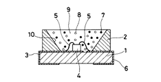
図1は本発明の半導体発光装置の実施例1の構造を示す断面図である。本実施例は表面実装型と言われているLEDで、基板1の表面に形成された回路パターンの上方に擂鉢状の凹部を有する反射枠2が設けられ、凹部の底面の第一の回路パターン3上にLEDチップ4が載設されている。そして、LEDチップ4の上面に設けられた2つの電極の一方はボンディングワイヤ5を介して第一の回路パターン3に接続されて電気的導通が図られ、他方の電極はボンディングワイヤ5を介して第一の回路パターン3とは分離された第二の回路パターン6に接続されて電気的導通が図られている。さらに、反射枠2に設けられた凹部に、光透過性樹脂に蛍光体7と20〜80wt%の拡散剤8とを混入した波長変換部材9が充填され、LEDチップ4を封止している。なお、反射枠2は高反射部材から成っており、凹部の内側面10は特別な反射処理を施さないで反射面を形成しているが、凹部の内側面10に反射率の高いアルミニウム、銀などを蒸着や塗装などの手法によって反射面を形成することも可能である。
FIG. 1 is a sectional view showing the structure of a semiconductor light emitting device according to a first embodiment of the present invention. This embodiment is an LED that is said to be a surface-mount type, in which a
このような構成のLEDにおいて、LEDチップ4から出射されて波長変換部材9に入射した光が蛍光体7および拡散剤8によってどのような作用を受け、蛍光体7と拡散剤8との光学的な関係がどのようなものであるかを模式的に示したものが図2である。LEDチップ4から出射されて波長変換部材9に入射した光を直接受光した蛍光体p1、p2およびp3は、それぞれ受光した光によって励起されて受光した光よりも長波長に波長変換された光を放出する。また、蛍光体p1、p2、およびp3の夫々の陰になってLEDチップ4から出射された光が直接受光できない(点線の矢印で表示)蛍光体p4、p6、およびp7と拡散剤d1の陰なってLEDチップ4から出射された光が直接受光できない(点線の矢印で表示)蛍光体p5は夫々拡散剤d1の散乱光、拡散剤d2およびd3の散乱光、拡散剤d3の散乱光、拡散剤d2の散乱光を受光し、受光した光によって励起されて受光した光よりも長波長に波長変換された光を放出する。
In the LED having such a configuration, the light emitted from the LED chip 4 and incident on the
このように、波長変換部材を構成する蛍光体は、LEDチップから出射された光と、1個の拡散剤で散乱された散乱光と、複数の拡散剤で散乱された複数の散乱光とが組み合わされた光を受光し、受光した光によって励起されて受光した光よりも長波長に波長変換された光を放出するものである。 As described above, the phosphor constituting the wavelength conversion member includes light emitted from the LED chip, scattered light scattered by one diffusing agent, and a plurality of scattered lights scattered by a plurality of diffusing agents. The combined light is received, and is excited by the received light and emits light whose wavelength is converted to a longer wavelength than the received light.
また、図2には示していないが、波長変換部材を構成する蛍光体が2種類以上の場合、蛍光体で波長変換された光が別の種類の蛍光体を励起して波長変換させるといったような波長変換の連鎖反応が生じることになる。このとき、連鎖する波長変換の夫々の過程で波長変換された光の一部はそのまま外部に放出されることになる。また、夫々の過程で蛍光体が1個あるいは複数の拡散剤による複数の散乱光の影響を受けることにもなる。さらに、蛍光体は複数の波長が混合された光を受けて励起されることにもなる。 Although not shown in FIG. 2, when two or more types of phosphors constitute the wavelength conversion member, the wavelength-converted light by the phosphor excites another type of phosphor to convert the wavelength. As a result, a chain reaction of wavelength conversion occurs. At this time, part of the light that has been wavelength-converted in each of the chained wavelength conversion processes is directly emitted to the outside. Further, in each process, the phosphor is affected by a plurality of scattered lights by one or a plurality of diffusing agents. Furthermore, the phosphor is excited by receiving light in which a plurality of wavelengths are mixed.
このように、LEDチップから出射された光をもとに、蛍光体と拡散剤とが複雑に関連する光の流れを構成しており、波長変換部材の内部に存在する多種の波長の光は混合されて分散され、色調のバラツキの少ない光を外部に放出することになる。 Thus, based on the light emitted from the LED chip, the phosphor and the diffusing agent constitute a complicated flow of light, and the light of various wavelengths existing inside the wavelength conversion member is Light that is mixed and dispersed and has little variation in color tone is emitted to the outside.
また、波長変換部材に蛍光体と共に20〜80wt%という比較的高濃度の拡散剤が混入されており、LEDチップから出射された光が直接至らない蛍光体であっても複数の拡散剤で散乱された光を受光することができるため、波長変換効率の良い高輝度のLEDが実現できる。 In addition, a relatively high concentration diffusing agent of 20 to 80 wt% is mixed with the phosphor in the wavelength conversion member, and even the phosphor that does not directly reach the light emitted from the LED chip is scattered by a plurality of diffusing agents. Therefore, a high-brightness LED with good wavelength conversion efficiency can be realized.
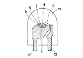
図3は本発明の半導体発光装置の実施例2の構造を示す断面図である。本実施例は砲弾型とも言われているLEDで、2本のリードフレーム11,12の一方の先端部に内側面を反射面とする擂鉢状の凹部が形成され、凹部の底面にLEDチップ4が載設されている。そして、LEDチップ4の上面に設けられた2つの電極の一方はボンディングワイヤ5を介してリードフレーム11に接続されて電気的導通が図られ、他方の電極はボンディングワイヤ5を介してリードフレーム12に接続されて電気的導通が図られている。そして、LEDチップ4が載設された凹部に、光透過性樹脂に蛍光体7と20〜80wt%の拡散剤8とを混入した波長変換部材9が充填され、LEDチップ4を封止している。さらに、LEDチップ4が載設されたリードフレーム11先端部は透明樹脂レンズ13で覆われている。
FIG. 3 is a cross-sectional view showing the structure of a second embodiment of the semiconductor light emitting device of the present invention. This embodiment is an LED that is also referred to as a shell type, and a mortar-shaped recess having an inner surface as a reflection surface is formed at one end of two
本実施例で、LEDチップ4が載設された凹部に充填された波長変換部材9の働きは、上述した実施例1の中で図2を参照して説明した内容と同様である。本実施例では、LEDチップ4が載設されたリードフレーム11の先端部を凸状の透明樹脂レンズ13で覆うことによって、ボンディングワイヤ5を振動や衝撃などの外部応力から保護し、波長変換部材9に混入された蛍光体7および拡散剤8を湿気などの周囲環境や機械的摩擦から保護し、LEDチップ4から出射されて波長変換部材9内を導光されて波長変換された光を外部に放出する際に光を集光させるようにレンズ効果を持たせたものである。
In this embodiment, the function of the
図4は本発明の半導体発光装置の実施例3の構造を示す断面図である。本実施例は上述した実施例2と同様に砲弾型のLEDである。2本のリードフレーム11,12の一方の先端部に内側面を反射面とする擂鉢状の凹部が形成され、凹部の底面にLEDチップ4が載設されている。そして、LEDチップ4の上面に設けられた2つの電極の一方はボンディングワイヤ5を介してリードフレーム11に接続されて電気的導通が図られ、他方の電極はボンディングワイヤ5を介してリードフレーム12に接続されて電気的導通が図られている。そして、LEDチップ4が載設されたリードフレーム11先端部は光透過性樹脂に蛍光体7と20〜80wt%の拡散剤8とを混入した波長変換部材9で覆われ、凸状のレンズが形成されている。
4 is a cross-sectional view showing the structure of a semiconductor light emitting device according to a third embodiment of the present invention. This embodiment is a bullet-type LED as in the second embodiment. A mortar-shaped recess having an inner surface as a reflection surface is formed at one end of the two
本実施例は、LEDチップ4が載設されたリードフレーム11の先端部を蛍光体7と20〜80wt%の拡散剤8とを混入した波長変換部材9で覆って凸状のレンズを形成したものであり、波長変換部材9の働きは上述した実施例1の中で図2を参照して説明した内容と同様である。ただし、LEDチップ4が載設されたリードフレーム11の先端部を波長変換部材9で一括封止できるため作業工数が少なく、工数削減による製造コストの低減に寄与するものである。
In this embodiment, the tip portion of the
なお、上述した実施例1〜実施例3で使用される光透過性樹脂はエポキシ樹脂、シリコーン樹脂、アクリル系樹脂およびシクロオレフィン系樹脂のなかから選択され、蛍光体は希土類を付活したアルミン酸塩、希土類を付活したチオ没食子酸塩および希土類を付活したオルトケイ酸塩のなかから選択され、拡散剤は酸化チタン、アルミナ及びシリカのなかから選択される。 The light-transmitting resin used in Examples 1 to 3 described above is selected from an epoxy resin, a silicone resin, an acrylic resin, and a cycloolefin resin, and the phosphor is aluminate activated with a rare earth. The salt, thiogallate activated by rare earth and orthosilicate activated by rare earth are selected, and the diffusing agent is selected from titanium oxide, alumina and silica.
また、光透過性樹脂に蛍光体と共に混入する拡散剤を20〜80wt%としたのは、20wt%より少ない場合は拡散剤を混入することによる高輝度化の効果が十分ではなく、80wt%より多くなると光透過性樹脂の粘度が高くなり、非常に固いペースト状態となって取り扱いが難しくなり、接着性も低下して封止樹脂としての機能を果たさなくなるためである。 Also, the reason why the diffusing agent mixed with the phosphor in the light transmitting resin is set to 20 to 80 wt% is that if the amount is less than 20 wt%, the effect of increasing the brightness by mixing the diffusing agent is not sufficient. If the amount is increased, the viscosity of the light-transmitting resin becomes high, and it becomes a very hard paste state, which is difficult to handle, and the adhesiveness is also lowered, so that the function as a sealing resin is not achieved.
本発明の実施例で使用されるLEDチップは、紫外光、青色光および緑色光を発光する3種類のLEDチップから選ばれ、種々の蛍光体との込み合わせによってLEDに求められる色調を実現する。その際、LEDチップは単独で使用される場合と、発光色の異なるLEDチップを組み合わせて使用される場合とがあり、紫外LEDチップは単独で使用されるが、可視光を発光する青色LEDチップと緑色LEDとは単独で使用される場合と、組み合わせて使用される場合とがある。 The LED chip used in the embodiment of the present invention is selected from three types of LED chips that emit ultraviolet light, blue light, and green light, and realizes the color tone required for the LED by combining with various phosphors. . At that time, the LED chip may be used alone or in combination with LED chips having different emission colors, and the ultraviolet LED chip is used alone, but the blue LED chip that emits visible light. And green LED may be used alone or in combination.
以上のように、本発明の半導体発光装置は、光を受けて受けた光よりも長波長へ波長変換する蛍光体と、光を受けて受けた光を散乱する拡散剤とが光透過性樹脂に混入された波長変換部材で封止されているため、蛍光体が受光する光には、LEDチップから出射した光や、LEDチップから出射して拡散剤で散乱された光や、種類が異なる蛍光体で波長変換された光や、種類が異なる蛍光体で波長変換された光が拡散剤で散乱された光などがある。特に、本発明の場合、光透過性樹脂に混入する拡散剤を20〜80wt%と比較的高濃度にしているので蛍光体が拡散剤で散乱された光を受光する割合が大きい。その結果、蛍光体で波長変換される光の光量が増加し、高輝度のLEDが実現できる。 As described above, in the semiconductor light emitting device of the present invention, the phosphor that converts the wavelength to a longer wavelength than the light received and the diffusing agent that scatters the received light is a light-transmitting resin. The light received by the phosphor is different in the light emitted from the LED chip, the light emitted from the LED chip and scattered by the diffusing agent, and the type. There are light that has been wavelength-converted by a phosphor and light in which light that has been wavelength-converted by a different type of phosphor is scattered by a diffusing agent. In particular, in the case of the present invention, since the diffusing agent mixed in the light transmissive resin has a relatively high concentration of 20 to 80 wt%, the phosphor receives a large proportion of light scattered by the diffusing agent. As a result, the amount of light whose wavelength is converted by the phosphor increases, and a high-brightness LED can be realized.
また、蛍光体には多様な光路を経て多種類の波長が混合された光が様々な方向から入射し、波長変換されて様々な方向に放射される。従って、波長変換部材内で波長変換されて混合された光は分散され、色調のバラツキの少ない光を発するLEDが実現できる。 In addition, light in which various types of wavelengths are mixed is incident on the phosphor from various directions through various optical paths, and the wavelength is converted and emitted in various directions. Therefore, the light that is wavelength-converted and mixed in the wavelength conversion member is dispersed, and an LED that emits light with little variation in color tone can be realized.
さらに、光透過性樹脂よりも熱膨張係数の小さい拡散剤の濃度を高くすることにより、波長変換部材内の光透過性樹脂の占める割合が減って、光透過性樹脂の絶対膨張体積が減少し、波長変換部材の熱膨張係数が小さくなる。その結果、半田リフローなどのLED実装時にLEDに外部から加わる熱やLEDの点灯時にLEDチップから発生する熱によって封止樹脂が膨張し、その応力を受けてLEDチップの破壊およびボンディングワイヤの切断などの不具合を発生させる要因を軽減させることができ、LEDの信頼性を向上させることができる。などの優れた効果を奏するものである。 Furthermore, by increasing the concentration of the diffusing agent having a smaller thermal expansion coefficient than the light-transmitting resin, the proportion of the light-transmitting resin in the wavelength conversion member decreases, and the absolute expansion volume of the light-transmitting resin decreases. The thermal expansion coefficient of the wavelength conversion member becomes small. As a result, the sealing resin expands due to heat applied to the LED from the outside during LED mounting, such as solder reflow, and heat generated from the LED chip when the LED is turned on, and the LED chip is destroyed and the bonding wire is cut by receiving the stress. This can reduce the cause of the problem and improve the reliability of the LED. It has excellent effects such as.
1 基板
2 反射枠
3 第一の回路パターン
4 LEDチップ
5 ボンディングワイヤ
6 第二の回路パターン
7 蛍光体
8 拡散剤
9 波長変換部材
10 内側面
11 第一のリードフレーム
12 第二のリードフレーム
13 樹脂レンズ
p1〜p7 蛍光体
d1〜d3 拡散剤
DESCRIPTION OF
Claims (6)
Priority Applications (3)
| Application Number | Priority Date | Filing Date | Title |
|---|---|---|---|
| JP2003324884A JP2005093712A (en) | 2003-09-17 | 2003-09-17 | Semiconductor light emitting device |
| CNA2004100465931A CN1599087A (en) | 2003-09-17 | 2004-06-11 | Semiconductor light-emitting device |
| US10/901,991 US20050057144A1 (en) | 2003-09-17 | 2004-07-30 | Semiconductor light-emitting device |
Applications Claiming Priority (1)
| Application Number | Priority Date | Filing Date | Title |
|---|---|---|---|
| JP2003324884A JP2005093712A (en) | 2003-09-17 | 2003-09-17 | Semiconductor light emitting device |
Publications (2)
| Publication Number | Publication Date |
|---|---|
| JP2005093712A true JP2005093712A (en) | 2005-04-07 |
| JP2005093712A5 JP2005093712A5 (en) | 2006-10-05 |
Family
ID=34270081
Family Applications (1)
| Application Number | Title | Priority Date | Filing Date |
|---|---|---|---|
| JP2003324884A Pending JP2005093712A (en) | 2003-09-17 | 2003-09-17 | Semiconductor light emitting device |
Country Status (3)
| Country | Link |
|---|---|
| US (1) | US20050057144A1 (en) |
| JP (1) | JP2005093712A (en) |
| CN (1) | CN1599087A (en) |
Cited By (7)
| Publication number | Priority date | Publication date | Assignee | Title |
|---|---|---|---|---|
| JP2006308859A (en) * | 2005-04-28 | 2006-11-09 | Mitsubishi Chemicals Corp | Display device |
| JP2006324486A (en) * | 2005-05-19 | 2006-11-30 | Mitsubishi Electric Corp | Semiconductor light emitting device |
| WO2008015833A1 (en) * | 2006-08-02 | 2008-02-07 | Tokai Kogaku Co., Ltd | Fluorescent light emitting device |
| JP2009094351A (en) * | 2007-10-10 | 2009-04-30 | Nichia Corp | Light emitting device, and manufacturing method thereof |
| US8766298B2 (en) | 2006-09-01 | 2014-07-01 | Cree, Inc. | Encapsulant profile for light emitting diodes |
| JP2015062226A (en) * | 2013-09-23 | 2015-04-02 | 弘凱光電(深セン)有限公司 | Light emitting diode package structure for preventing lateral light leakage and method of manufacturing the same |
| US9768364B2 (en) | 2014-05-21 | 2017-09-19 | Nichia Corporation | Light emitting device and method of manufacturing the same |
Families Citing this family (28)
| Publication number | Priority date | Publication date | Assignee | Title |
|---|---|---|---|---|
| CN100373646C (en) * | 2005-03-25 | 2008-03-05 | 李洲科技股份有限公司 | Multi-wavelength LED structure and making process thereof |
| KR100666189B1 (en) | 2005-06-30 | 2007-01-09 | 서울반도체 주식회사 | Light emitting device |
| KR100665222B1 (en) * | 2005-07-26 | 2007-01-09 | 삼성전기주식회사 | Led package with diffusing material and method of manufacturing the same |
| US7329907B2 (en) | 2005-08-12 | 2008-02-12 | Avago Technologies, Ecbu Ip Pte Ltd | Phosphor-converted LED devices having improved light distribution uniformity |
| JP4945106B2 (en) * | 2005-09-08 | 2012-06-06 | スタンレー電気株式会社 | Semiconductor light emitting device |
| KR100691440B1 (en) * | 2005-11-15 | 2007-03-09 | 삼성전기주식회사 | Led package |
| JP4417906B2 (en) * | 2005-12-16 | 2010-02-17 | 株式会社東芝 | Light emitting device and manufacturing method thereof |
| JP2007273562A (en) * | 2006-03-30 | 2007-10-18 | Toshiba Corp | Semiconductor light-emitting device |
| CN100418242C (en) * | 2006-05-17 | 2008-09-10 | 广州南科集成电子有限公司 | LED and method for fabricating same |
| WO2007141827A1 (en) * | 2006-05-30 | 2007-12-13 | Fujikura Ltd. | Light emitting element mounting substrate, light source, lighting device, display device, traffic light, and method for fabricating light emitting element mounting substrate |
| CN101467270B (en) * | 2006-06-14 | 2013-03-27 | 皇家飞利浦电子股份有限公司 | Lighting device |
| US20080035942A1 (en) * | 2006-08-08 | 2008-02-14 | Lg Electronics Inc. | Light emitting device package and method for manufacturing the same |
| JP4961978B2 (en) * | 2006-11-30 | 2012-06-27 | 日亜化学工業株式会社 | Light emitting device and manufacturing method thereof |
| KR101423723B1 (en) * | 2007-10-29 | 2014-08-04 | 서울바이오시스 주식회사 | Light emitting diode package |
| TWI426206B (en) | 2008-12-25 | 2014-02-11 | Au Optronics Corp | Light emitting diode apparatus |
| US8547009B2 (en) | 2009-07-10 | 2013-10-01 | Cree, Inc. | Lighting structures including diffuser particles comprising phosphor host materials |
| US9385285B2 (en) * | 2009-09-17 | 2016-07-05 | Koninklijke Philips N.V. | LED module with high index lens |
| JP5734581B2 (en) * | 2010-05-21 | 2015-06-17 | シャープ株式会社 | Semiconductor light emitting device |
| TWI427371B (en) * | 2010-10-06 | 2014-02-21 | Au Optronics Corp | Light source module and liquid crystal display |
| CN101963315B (en) * | 2010-10-14 | 2016-01-20 | 友达光电股份有限公司 | Light source module and liquid crystal display |
| CN102610602A (en) * | 2011-01-25 | 2012-07-25 | 四川柏狮光电技术有限公司 | High-resolution LED (light emitting diode) light source made of single-package-based material and manufacturing process of high-resolution LED light source |
| CN102720957A (en) * | 2011-12-04 | 2012-10-10 | 深圳市光峰光电技术有限公司 | Light emitting device, projection device and illuminating device |
| CN103107266A (en) * | 2012-12-18 | 2013-05-15 | 浙江中宙光电股份有限公司 | Light emitting diode (LED) white light device and manufacturing method thereof |
| CN103633230B (en) * | 2013-12-18 | 2016-05-11 | 东南大学 | A kind of fluorescent material of eliminating white light LED color temperature deviation |
| CN103913799A (en) * | 2014-04-09 | 2014-07-09 | 常州巨猫电子科技有限公司 | LED light guide column and application thereof |
| DE102015101216A1 (en) * | 2015-01-28 | 2016-07-28 | Osram Opto Semiconductors Gmbh | Optoelectronic arrangement with radiation conversion element and method for producing a radiation conversion element |
| CN105405951A (en) * | 2015-12-20 | 2016-03-16 | 合肥艾斯克光电科技有限责任公司 | Packaging method for LED white-light lamp |
| KR102389815B1 (en) * | 2017-06-05 | 2022-04-22 | 삼성전자주식회사 | Quantum dot glass cell and light emitting device package comprising the same |
Family Cites Families (10)
| Publication number | Priority date | Publication date | Assignee | Title |
|---|---|---|---|---|
| US5122733A (en) * | 1986-01-15 | 1992-06-16 | Karel Havel | Variable color digital multimeter |
| JP3420612B2 (en) * | 1993-06-25 | 2003-06-30 | 株式会社東芝 | LED lamp |
| KR100629544B1 (en) * | 1996-06-26 | 2006-09-27 | 오스람 게젤샤프트 미트 베쉬랭크터 하프퉁 | Light-emitting semiconductor component with luminescence conversion element |
| JP2001196642A (en) * | 2000-01-11 | 2001-07-19 | Toyoda Gosei Co Ltd | Light emitting device |
| JP4406490B2 (en) * | 2000-03-14 | 2010-01-27 | 株式会社朝日ラバー | Light emitting diode |
| MY145695A (en) * | 2001-01-24 | 2012-03-30 | Nichia Corp | Light emitting diode, optical semiconductor device, epoxy resin composition suited for optical semiconductor device, and method for manufacturing the same |
| US6642652B2 (en) * | 2001-06-11 | 2003-11-04 | Lumileds Lighting U.S., Llc | Phosphor-converted light emitting device |
| TW511303B (en) * | 2001-08-21 | 2002-11-21 | Wen-Jr He | A light mixing layer and method |
| US6870311B2 (en) * | 2002-06-07 | 2005-03-22 | Lumileds Lighting U.S., Llc | Light-emitting devices utilizing nanoparticles |
| TW558775B (en) * | 2002-06-27 | 2003-10-21 | Solidlite Corp | Package of compound type LED |
-
2003
- 2003-09-17 JP JP2003324884A patent/JP2005093712A/en active Pending
-
2004
- 2004-06-11 CN CNA2004100465931A patent/CN1599087A/en active Pending
- 2004-07-30 US US10/901,991 patent/US20050057144A1/en not_active Abandoned
Cited By (11)
| Publication number | Priority date | Publication date | Assignee | Title |
|---|---|---|---|---|
| JP2006308859A (en) * | 2005-04-28 | 2006-11-09 | Mitsubishi Chemicals Corp | Display device |
| JP2006324486A (en) * | 2005-05-19 | 2006-11-30 | Mitsubishi Electric Corp | Semiconductor light emitting device |
| JP4727297B2 (en) * | 2005-05-19 | 2011-07-20 | 三菱電機株式会社 | Semiconductor light emitting device |
| WO2008015833A1 (en) * | 2006-08-02 | 2008-02-07 | Tokai Kogaku Co., Ltd | Fluorescent light emitting device |
| JP2008041739A (en) * | 2006-08-02 | 2008-02-21 | Tokai Kogaku Kk | Fluorescent device |
| US8766298B2 (en) | 2006-09-01 | 2014-07-01 | Cree, Inc. | Encapsulant profile for light emitting diodes |
| JP2009094351A (en) * | 2007-10-10 | 2009-04-30 | Nichia Corp | Light emitting device, and manufacturing method thereof |
| JP2015062226A (en) * | 2013-09-23 | 2015-04-02 | 弘凱光電(深セン)有限公司 | Light emitting diode package structure for preventing lateral light leakage and method of manufacturing the same |
| US9236541B2 (en) | 2013-09-23 | 2016-01-12 | Brightek Optoelectronic (Shenzhen) Co., Ltd. | LED package structures for preventing lateral light leakage and method of manufacturing the same |
| US9768364B2 (en) | 2014-05-21 | 2017-09-19 | Nichia Corporation | Light emitting device and method of manufacturing the same |
| US10763405B2 (en) | 2014-05-21 | 2020-09-01 | Nichia Corporation | Light emitting device and method of manufacturing the same |
Also Published As
| Publication number | Publication date |
|---|---|
| US20050057144A1 (en) | 2005-03-17 |
| CN1599087A (en) | 2005-03-23 |
Similar Documents
| Publication | Publication Date | Title |
|---|---|---|
| JP2005093712A (en) | Semiconductor light emitting device | |
| JP5284006B2 (en) | Light emitting device | |
| US7586127B2 (en) | Light emitting diode | |
| KR101200400B1 (en) | White light emitting diode | |
| KR100891810B1 (en) | White light emitting device | |
| JP5919504B2 (en) | Light emitting device | |
| JP5557828B2 (en) | Light emitting device | |
| US10096749B2 (en) | Illumination light source, illumination apparatus, outdoor illumination apparatus, and vehicle headlight | |
| JP2010034183A (en) | Light-emitting device | |
| JP2010034184A (en) | Light-emitting device | |
| US20070159064A1 (en) | White light emitting device | |
| JP2007123438A (en) | Phosphor plate and light emitting device with same | |
| JP2007088348A (en) | Illumination device, back light device, and liquid crystal display | |
| JP2009267039A (en) | Light-emitting device | |
| JP2007134656A (en) | Fluorescent board and light emitting device having it | |
| JP2007134606A (en) | White light source | |
| JP2008028181A (en) | Lighting device | |
| JP2007005549A (en) | White-light emitting diode lamp | |
| JP4591106B2 (en) | White light emitting device | |
| JP2005332951A (en) | Light emitting device | |
| JP2007243056A (en) | Light emitting device | |
| JP2007027310A (en) | High color-rendering light emitting diode lamp unit | |
| JP2017054994A (en) | Light emitting device and luminaire | |
| JP2007081159A (en) | Light emitting device and display device | |
| JP2002344021A (en) | Light-emitting device |
Legal Events
| Date | Code | Title | Description |
|---|---|---|---|
| A521 | Request for written amendment filed |
Free format text: JAPANESE INTERMEDIATE CODE: A523 Effective date: 20060818 |
|
| A621 | Written request for application examination |
Free format text: JAPANESE INTERMEDIATE CODE: A621 Effective date: 20060818 |
|
| A977 | Report on retrieval |
Free format text: JAPANESE INTERMEDIATE CODE: A971007 Effective date: 20090818 |
|
| A131 | Notification of reasons for refusal |
Free format text: JAPANESE INTERMEDIATE CODE: A131 Effective date: 20090915 |
|
| A02 | Decision of refusal |
Free format text: JAPANESE INTERMEDIATE CODE: A02 Effective date: 20100126 |