JP2005092969A - Nonvolatile semiconductor memory - Google Patents
Nonvolatile semiconductor memory Download PDFInfo
- Publication number
- JP2005092969A JP2005092969A JP2003323633A JP2003323633A JP2005092969A JP 2005092969 A JP2005092969 A JP 2005092969A JP 2003323633 A JP2003323633 A JP 2003323633A JP 2003323633 A JP2003323633 A JP 2003323633A JP 2005092969 A JP2005092969 A JP 2005092969A
- Authority
- JP
- Japan
- Prior art keywords
- circuit
- signal
- block
- gate
- level
- Prior art date
- Legal status (The legal status is an assumption and is not a legal conclusion. Google has not performed a legal analysis and makes no representation as to the accuracy of the status listed.)
- Pending
Links
Images


Classifications
-
- G—PHYSICS
- G11—INFORMATION STORAGE
- G11C—STATIC STORES
- G11C29/00—Checking stores for correct operation ; Subsequent repair; Testing stores during standby or offline operation
- G11C29/04—Detection or location of defective memory elements, e.g. cell constructio details, timing of test signals
- G11C29/50—Marginal testing, e.g. race, voltage or current testing
-
- B—PERFORMING OPERATIONS; TRANSPORTING
- B08—CLEANING
- B08B—CLEANING IN GENERAL; PREVENTION OF FOULING IN GENERAL
- B08B11/00—Cleaning flexible or delicate articles by methods or apparatus specially adapted thereto
- B08B11/04—Cleaning flexible or delicate articles by methods or apparatus specially adapted thereto specially adapted for plate glass, e.g. prior to manufacture of windshields
-
- C—CHEMISTRY; METALLURGY
- C03—GLASS; MINERAL OR SLAG WOOL
- C03C—CHEMICAL COMPOSITION OF GLASSES, GLAZES OR VITREOUS ENAMELS; SURFACE TREATMENT OF GLASS; SURFACE TREATMENT OF FIBRES OR FILAMENTS MADE FROM GLASS, MINERALS OR SLAGS; JOINING GLASS TO GLASS OR OTHER MATERIALS
- C03C23/00—Other surface treatment of glass not in the form of fibres or filaments
- C03C23/0085—Drying; Dehydroxylation
-
- G—PHYSICS
- G11—INFORMATION STORAGE
- G11C—STATIC STORES
- G11C16/00—Erasable programmable read-only memories
- G11C16/02—Erasable programmable read-only memories electrically programmable
- G11C16/06—Auxiliary circuits, e.g. for writing into memory
- G11C16/26—Sensing or reading circuits; Data output circuits
-
- G—PHYSICS
- G11—INFORMATION STORAGE
- G11C—STATIC STORES
- G11C16/00—Erasable programmable read-only memories
- G11C16/02—Erasable programmable read-only memories electrically programmable
- G11C16/06—Auxiliary circuits, e.g. for writing into memory
- G11C16/34—Determination of programming status, e.g. threshold voltage, overprogramming or underprogramming, retention
- G11C16/3436—Arrangements for verifying correct programming or erasure
- G11C16/344—Arrangements for verifying correct erasure or for detecting overerased cells
- G11C16/3445—Circuits or methods to verify correct erasure of nonvolatile memory cells
-
- G—PHYSICS
- G11—INFORMATION STORAGE
- G11C—STATIC STORES
- G11C16/00—Erasable programmable read-only memories
- G11C16/02—Erasable programmable read-only memories electrically programmable
- G11C16/06—Auxiliary circuits, e.g. for writing into memory
- G11C16/34—Determination of programming status, e.g. threshold voltage, overprogramming or underprogramming, retention
- G11C16/3436—Arrangements for verifying correct programming or erasure
- G11C16/3454—Arrangements for verifying correct programming or for detecting overprogrammed cells
- G11C16/3459—Circuits or methods to verify correct programming of nonvolatile memory cells
-
- G—PHYSICS
- G11—INFORMATION STORAGE
- G11C—STATIC STORES
- G11C29/00—Checking stores for correct operation ; Subsequent repair; Testing stores during standby or offline operation
- G11C29/02—Detection or location of defective auxiliary circuits, e.g. defective refresh counters
-
- G—PHYSICS
- G11—INFORMATION STORAGE
- G11C—STATIC STORES
- G11C29/00—Checking stores for correct operation ; Subsequent repair; Testing stores during standby or offline operation
- G11C29/02—Detection or location of defective auxiliary circuits, e.g. defective refresh counters
- G11C29/025—Detection or location of defective auxiliary circuits, e.g. defective refresh counters in signal lines
-
- G—PHYSICS
- G11—INFORMATION STORAGE
- G11C—STATIC STORES
- G11C29/00—Checking stores for correct operation ; Subsequent repair; Testing stores during standby or offline operation
- G11C29/04—Detection or location of defective memory elements, e.g. cell constructio details, timing of test signals
- G11C29/08—Functional testing, e.g. testing during refresh, power-on self testing [POST] or distributed testing
- G11C29/12—Built-in arrangements for testing, e.g. built-in self testing [BIST] or interconnection details
- G11C29/12005—Built-in arrangements for testing, e.g. built-in self testing [BIST] or interconnection details comprising voltage or current generators
-
- G—PHYSICS
- G11—INFORMATION STORAGE
- G11C—STATIC STORES
- G11C29/00—Checking stores for correct operation ; Subsequent repair; Testing stores during standby or offline operation
- G11C29/70—Masking faults in memories by using spares or by reconfiguring
- G11C29/78—Masking faults in memories by using spares or by reconfiguring using programmable devices
- G11C29/80—Masking faults in memories by using spares or by reconfiguring using programmable devices with improved layout
-
- G—PHYSICS
- G11—INFORMATION STORAGE
- G11C—STATIC STORES
- G11C29/00—Checking stores for correct operation ; Subsequent repair; Testing stores during standby or offline operation
- G11C29/70—Masking faults in memories by using spares or by reconfiguring
- G11C29/78—Masking faults in memories by using spares or by reconfiguring using programmable devices
- G11C29/83—Masking faults in memories by using spares or by reconfiguring using programmable devices with reduced power consumption
- G11C29/832—Masking faults in memories by using spares or by reconfiguring using programmable devices with reduced power consumption with disconnection of faulty elements
-
- G—PHYSICS
- G11—INFORMATION STORAGE
- G11C—STATIC STORES
- G11C5/00—Details of stores covered by group G11C11/00
- G11C5/02—Disposition of storage elements, e.g. in the form of a matrix array
- G11C5/025—Geometric lay-out considerations of storage- and peripheral-blocks in a semiconductor storage device
-
- G—PHYSICS
- G11—INFORMATION STORAGE
- G11C—STATIC STORES
- G11C8/00—Arrangements for selecting an address in a digital store
- G11C8/08—Word line control circuits, e.g. drivers, boosters, pull-up circuits, pull-down circuits, precharging circuits, for word lines
-
- G—PHYSICS
- G11—INFORMATION STORAGE
- G11C—STATIC STORES
- G11C16/00—Erasable programmable read-only memories
- G11C16/02—Erasable programmable read-only memories electrically programmable
- G11C16/04—Erasable programmable read-only memories electrically programmable using variable threshold transistors, e.g. FAMOS
-
- G—PHYSICS
- G11—INFORMATION STORAGE
- G11C—STATIC STORES
- G11C29/00—Checking stores for correct operation ; Subsequent repair; Testing stores during standby or offline operation
- G11C29/04—Detection or location of defective memory elements, e.g. cell constructio details, timing of test signals
- G11C29/08—Functional testing, e.g. testing during refresh, power-on self testing [POST] or distributed testing
- G11C29/12—Built-in arrangements for testing, e.g. built-in self testing [BIST] or interconnection details
- G11C2029/1202—Word line control
-
- G—PHYSICS
- G11—INFORMATION STORAGE
- G11C—STATIC STORES
- G11C29/00—Checking stores for correct operation ; Subsequent repair; Testing stores during standby or offline operation
- G11C29/04—Detection or location of defective memory elements, e.g. cell constructio details, timing of test signals
- G11C29/08—Functional testing, e.g. testing during refresh, power-on self testing [POST] or distributed testing
- G11C29/12—Built-in arrangements for testing, e.g. built-in self testing [BIST] or interconnection details
- G11C2029/4402—Internal storage of test result, quality data, chip identification, repair information
-
- G—PHYSICS
- G11—INFORMATION STORAGE
- G11C—STATIC STORES
- G11C29/00—Checking stores for correct operation ; Subsequent repair; Testing stores during standby or offline operation
- G11C29/04—Detection or location of defective memory elements, e.g. cell constructio details, timing of test signals
- G11C29/50—Marginal testing, e.g. race, voltage or current testing
- G11C2029/5006—Current
-
- G—PHYSICS
- G11—INFORMATION STORAGE
- G11C—STATIC STORES
- G11C29/00—Checking stores for correct operation ; Subsequent repair; Testing stores during standby or offline operation
- G11C29/70—Masking faults in memories by using spares or by reconfiguring
- G11C29/78—Masking faults in memories by using spares or by reconfiguring using programmable devices
- G11C29/80—Masking faults in memories by using spares or by reconfiguring using programmable devices with improved layout
- G11C29/816—Masking faults in memories by using spares or by reconfiguring using programmable devices with improved layout for an application-specific layout
- G11C29/82—Masking faults in memories by using spares or by reconfiguring using programmable devices with improved layout for an application-specific layout for EEPROMs
Landscapes
- Engineering & Computer Science (AREA)
- Microelectronics & Electronic Packaging (AREA)
- Chemical & Material Sciences (AREA)
- Life Sciences & Earth Sciences (AREA)
- Chemical Kinetics & Catalysis (AREA)
- General Chemical & Material Sciences (AREA)
- Geochemistry & Mineralogy (AREA)
- Materials Engineering (AREA)
- Organic Chemistry (AREA)
- For Increasing The Reliability Of Semiconductor Memories (AREA)
- Read Only Memory (AREA)
Abstract
Description
この発明は、不揮発性半導体記憶装置に関し、より特定的には、消去単位がブロック毎である不揮発性半導体記憶装置に関する。 The present invention relates to a nonvolatile semiconductor memory device, and more particularly to a nonvolatile semiconductor memory device in which an erase unit is a block.
不揮発性半導体記憶装置の一つであるフラッシュメモリは、消去単位がブロック毎である。具体的には、メモリセルのワード線とウェル&ソース線との間に高電圧を印加することによって、フラッシュメモリの消去動作が行なわれる。 A flash memory, which is one of nonvolatile semiconductor memory devices, has an erase unit for each block. Specifically, the erase operation of the flash memory is performed by applying a high voltage between the word line and the well & source line of the memory cell.
フラッシュメモリのメモリマット内において、ワード線とビット線との間のショート、またはワード線とウェル&ソース線との間のショートが発生すると、それに起因したリーク電流により、消去動作時にメモリセルのワード線とウェル&ソース線との間に印加される高電圧のレベルが低下する。これにより、当該フラッシュメモリにおいて消去不良が発生する。フラッシュメモリの消去単位はブロック毎であるため、消去不良もブロック単位となる。 When a short circuit between a word line and a bit line or a short circuit between a word line and a well & source line occurs in a memory mat of a flash memory, the word of the memory cell is erased during the erase operation due to a leakage current caused by the short circuit. The level of the high voltage applied between the line and the well & source line is reduced. As a result, an erasure failure occurs in the flash memory. Since the erasure unit of the flash memory is for each block, the erasure defect is also a block unit.
したがって、フラッシュメモリにおける消去不良を救済するためには、ブロック単位での置換を行なうためのスペアブロックが必要となる。フラッシュメモリにスペアブロックを搭載すると、チップ面積は必然的に増加する。そのため、周辺回路を如何にしてノーマルブロックと共有しチップ面積の増加を抑えるかが、フラッシュメモリのフロアプラン(回路配置設計)において重要である。 Therefore, in order to relieve the erasure failure in the flash memory, a spare block for performing replacement in block units is required. When a spare block is mounted on a flash memory, the chip area inevitably increases. Therefore, it is important in the flash memory floor plan (circuit layout design) how to share the peripheral circuit with the normal block and suppress the increase in the chip area.
フラッシュメモリのフロアプランは、フラッシュメモリ特有の高電圧発生回路による周辺回路への電源ノイズの影響を抑制する上でも重要である。また、フラッシュメモリのフロアプランは、自動配置配線ツールを使用してレイアウトされるロジック回路帯のアスペクト比(縦横比)を低減する上でも重要である。ロジック回路帯のアスペクト比を低減することにより、フラッシュメモリの集積度を向上させることができる。 The floor plan of the flash memory is also important for suppressing the influence of power supply noise on the peripheral circuits by the high voltage generation circuit unique to the flash memory. Further, the floor plan of the flash memory is important for reducing the aspect ratio (aspect ratio) of the logic circuit band laid out using the automatic placement and routing tool. By reducing the aspect ratio of the logic circuit band, the degree of integration of the flash memory can be improved.
また、フラッシュメモリにスペアブロックを搭載する場合、リーク電流によって生ずる不良ブロックの非選択処理が重要となる。フラッシュメモリのWT(Wafer Test)では全ブロック一括の電圧ストレス印加テストを実施するが、その際、不良ブロックでのリーク電流による電圧降下を抑制する必要がある。そのためには、不良ブロックに電圧ストレスが印加されないようにしなければならない。 In addition, when a spare block is mounted in a flash memory, it is important to perform a non-selection process for a defective block caused by a leak current. In the WT (Wafer Test) of the flash memory, a voltage stress application test is performed for all blocks at the same time. At this time, it is necessary to suppress a voltage drop due to a leakage current in a defective block. For this purpose, it is necessary to prevent voltage stress from being applied to the defective block.
従来の不揮発性半導体記憶装置(フラッシュメモリ)は、一括書込み・消去テストモード時に、昇圧回路の出力電圧を低下させるような不良番地を自動的に検出する。そして、その番地には高電圧ストレスがかからないよう不良番地を記憶回路に記憶することで、冗長回路使用前に行なわれるメモリセルへの一括書込み・消去試験を実現する。(たとえば、特許文献1参照)
しかしながら、従来の不揮発性半導体記憶装置は、フロアプランを考慮せず、駆動電圧発生回路から駆動される電位の変化をモニタすることにより不良ブロックの判定を行なっている。そのため、チップ面積が増大し、かつ不良ブロックのリーク電流を直接モニタすることができないという問題点があった。 However, the conventional nonvolatile semiconductor memory device determines a defective block by monitoring a change in potential driven from the drive voltage generation circuit without considering the floor plan. Therefore, there are problems that the chip area is increased and the leakage current of the defective block cannot be directly monitored.
この発明の目的は、チップ面積の増大を抑制しつつ、不良ブロックの非選択処理が可能な不揮発性半導体記憶装置を提供することである。 An object of the present invention is to provide a nonvolatile semiconductor memory device capable of non-selection processing of a defective block while suppressing an increase in chip area.
この発明のある局面による不揮発性半導体記憶装置は、平面形状がコの字型に配置されるメモリアレイと、メモリアレイの配置によって形成される凹部に配置されるアナログ回路およびロジック回路と、メモリアレイに接せず、かつアナログ回路およびロジック回路の近傍に配置される電源パッドとを備える。 A nonvolatile semiconductor memory device according to an aspect of the present invention includes a memory array having a U-shaped planar shape, an analog circuit and a logic circuit disposed in a recess formed by the memory array, and a memory array And a power supply pad disposed in the vicinity of the analog circuit and the logic circuit.
この発明の他の局面による不揮発性半導体記憶装置は、ノーマルブロックとスペアブロックとを含む複数のメモリブロックと、複数のメモリブロックごとのスペアブロック置換情報と不良スペアブロック情報とからなるブロック情報を格納するメモリアレイと、ブロック情報を受けて、複数のメモリブロックが良か不良かを判定するスペアブロック判定信号を出力するスペアブロック判定回路と、スペアブロック判定信号を受けて、複数のメモリブロックごとにデコードを行なうデコード回路とを備える。 A non-volatile semiconductor memory device according to another aspect of the present invention stores block information comprising a plurality of memory blocks including normal blocks and spare blocks, and spare block replacement information and defective spare block information for each of the plurality of memory blocks. A memory block that receives the block information, a spare block determination circuit that outputs a spare block determination signal for determining whether the plurality of memory blocks are good or defective, and a spare block determination signal for each of the plurality of memory blocks A decoding circuit for performing decoding.
この発明のさらに他の局面による不揮発性半導体記憶装置は、複数のワード線、複数のメインビット線、複数のサブビット線、および複数のメインビット線と複数のサブビット線とを制御信号に応じてそれぞれ電気的に接続/分離する複数の選択ゲートを有する不揮発性メモリアレイと、不揮発性メモリアレイにおけるリーク電流をモニタするアナログ回路とを備える。アナログ回路は、一定の内部高電圧を発生する内部高電圧発生回路と、ワード線のリーク電流に伴うワード線電圧を増幅するワード線アンプと、選択ゲートのリーク電流に伴う選択ゲート電圧を増幅する選択ゲートアンプと、内部高電圧およびワード線電圧を受けて、ワード線のリーク電流をモニタする第1のリークモニタ回路と、内部高電圧および選択ゲート電圧を受けて、選択ゲートのリーク電流をモニタする第2のリークモニタ回路とを含む。 According to still another aspect of the present invention, a nonvolatile semiconductor memory device includes a plurality of word lines, a plurality of main bit lines, a plurality of sub bit lines, and a plurality of main bit lines and a plurality of sub bit lines according to control signals. A nonvolatile memory array having a plurality of select gates that are electrically connected / separated, and an analog circuit that monitors a leakage current in the nonvolatile memory array are provided. The analog circuit includes an internal high voltage generation circuit that generates a constant internal high voltage, a word line amplifier that amplifies the word line voltage associated with the leakage current of the word line, and an amplification of the selection gate voltage associated with the leakage current of the selection gate. A selection gate amplifier, a first leakage monitor circuit that receives the internal high voltage and the word line voltage and monitors the leakage current of the word line, and a leakage current of the selection gate that receives the internal high voltage and the selection gate voltage A second leak monitor circuit.
この発明によれば、チップ面積の増大を抑制しつつ、不良ブロックの非選択処理が可能となる。 According to the present invention, it is possible to perform non-selection processing of defective blocks while suppressing an increase in chip area.
以下、この発明の実施の形態について図面を参照して詳しく説明する。なお、図中同一または相当部分には同一符号を付してその説明は繰り返さない。 Hereinafter, embodiments of the present invention will be described in detail with reference to the drawings. In the drawings, the same or corresponding parts are denoted by the same reference numerals and description thereof will not be repeated.
[実施の形態1]
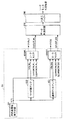
図1は、この発明の実施の形態1による不揮発性半導体記憶装置1Aの構成を示したブロック図である。
[Embodiment 1]
FIG. 1 is a block diagram showing a configuration of a nonvolatile
図1を参照して、実施の形態1の不揮発性半導体記憶装置1Aは、平面形状がコの字型に配置されたメモリアレイ2(図1の太線で囲まれた部分)と、アナログ回路91と、ロジック回路92と、制御回路93,94と、データパッド100と、電源パッド101と、アドレスパッド110とを備える。メモリアレイ2は、メモリマット10,20,30,40(たとえば28Mb)と、不良メモリセル情報記憶領域19と、メモリマット50,60(たとえば8Mb)と、スペアブロック11,21,22,31,32,41,42,51,52,61と、ロウプリデコーダ13,63と、ロウデコーダ14,24,34,44,54,64と、コラムデコーダ15,25,35,45,55,65と、センスアンプ71,73,74,76と、制御回路81とを含む。
Referring to FIG. 1, a nonvolatile
メモリマット10(バンク1とも称する)は、スペアブロック11を含む。ロウプリデコーダ13およびロウデコーダ14は、メモリマット10の図示しないワード線等を活性化する。コラムデコーダ15は、メモリマット10の図示しないビット線等を活性化する。不良メモリセル情報記憶領域19は、不揮発性メモリであって、ユーザーが書込みおよび消去ができない領域であり、ブロックごとの良/不良情報を格納することができる。
Memory mat 10 (also referred to as bank 1) includes a
メモリマット20(バンク2とも称する)は、スペアブロック21,22を含む。ロウデコーダ24は、メモリマット20の図示しないワード線等を活性化する。コラムデコーダ25は、メモリマット20の図示しないビット線等を活性化する。センスアンプ71は、メモリマット10,20に対して共通に設置され、メモリマット10,20における図示しないビット線対の電位差を検知増幅する。ここで、メモリマット10,20に対して共通に設置されるセンスアンプ70、およびコラムデコーダ15,25のより詳細な構成および動作について、図面を参照しながら説明する。
Memory mat 20 (also referred to as bank 2) includes
図2は、メモリマット10,20に対して共通に設置されるセンスアンプ70、およびコラムデコーダ15,25の構成を示した回路図である。
FIG. 2 is a circuit diagram showing a configuration of sense amplifier 70 and
図2を参照して、センスアンプ70は、リードセンスアンプ71Rと、ベリファイセンスアンプ71Vとを含む。 Referring to FIG. 2, sense amplifier 70 includes a read sense amplifier 71R and a verify sense amplifier 71V.
コラムデコーダ15は、NチャネルMOSトランジスタN11,N12,N13を含む。NチャネルMOSトランジスタN11は、メモリマット10からのメインビット線MBL1とノードND11との間に接続され、ゲートにコラム制御信号CAL_BANK1を受ける。NチャネルMOSトランジスタN12は、ノードND11とリードセンスアンプ71Rとの間に接続され、ゲートにコラム制御信号CAUE_BANK1を受ける。NチャネルMOSトランジスタN13は、ノードND11とベリファイセンスアンプ71Vとの間に接続され、ゲートにコラム制御信号CAUO_BANK1を受ける。
コラムデコーダ25は、NチャネルMOSトランジスタN14,N15,N16を含む。NチャネルMOSトランジスタN14は、メモリマット20からのメインビット線MBL2とノードND12との間に接続され、ゲートにコラム制御信号CAL_BANK2を受ける。NチャネルMOSトランジスタN15は、ノードND12とリードセンスアンプ71Rとの間に接続され、ゲートにコラム制御信号CAUE_BANK2を受ける。NチャネルMOSトランジスタN16は、ノードND12とベリファイセンスアンプ71Vとの間に接続され、ゲートにコラム制御信号CAUO_BANK2を受ける。
メモリマット10は、選択ゲートSG10,SG11(いずれもNチャネルMOSトランジスタ)と、メモリセルMC00,MC01,MC10,MC11とを含む。選択ゲートSG10は、メインビット線MBL1とサブビット線SBL10との間に接続され、ゲートが選択ゲート線SGL10に接続される。選択ゲートSG11は、メインビット線MBL1とサブビット線SBL11との間に接続され、ゲートが選択ゲート線SGL11に接続される。
メモリセルMC00は、サブビット線SBL10とソース線SL1との間に接続され、ゲートがワード線WL10に接続される。メモリセルMC01は、ソース線SL1とサブビット線SBL10との間に接続され、ゲートがワード線WL11に接続される。メモリセルMC10は、サブビット線SBL11とソース線SL1との間に接続され、ゲートがワード線WL10に接続される。メモリセルMC11は、ソース線SL1とサブビット線SBL11との間に接続され、ゲートがワード線WL11に接続される。 Memory cell MC00 is connected between sub-bit line SBL10 and source line SL1, and has its gate connected to word line WL10. Memory cell MC01 is connected between source line SL1 and sub-bit line SBL10, and has a gate connected to word line WL11. Memory cell MC10 is connected between sub-bit line SBL11 and source line SL1, and has its gate connected to word line WL10. Memory cell MC11 is connected between source line SL1 and sub-bit line SBL11, and has a gate connected to word line WL11.
メモリマット20は、選択ゲートSG20,SG21(いずれもNチャネルMOSトランジスタ)と、メモリセルMC20,MC21,MC30,MC31とを含む。選択ゲートSG20は、メインビット線MBL2とサブビット線SBL20との間に接続され、ゲートが選択ゲート線SGL20に接続される。選択ゲートSG21は、メインビット線MBL2とサブビット線SBL21との間に接続され、ゲートが選択ゲート線SGL21に接続される。
メモリセルMC20は、サブビット線SBL20とソース線SL2との間に接続され、ゲートがワード線WL20に接続される。メモリセルMC21は、ソース線SL2とサブビット線SBL20との間に接続され、ゲートがワード線WL11に接続される。メモリセルMC30は、サブビット線SBL21とソース線SL2との間に接続され、ゲートがワード線WL20に接続される。メモリセルMC31は、ソース線SL2とサブビット線SBL21との間に接続され、ゲートがワード線WL21に接続される。 Memory cell MC20 is connected between sub-bit line SBL20 and source line SL2, and has its gate connected to word line WL20. Memory cell MC21 is connected between source line SL2 and sub-bit line SBL20, and has its gate connected to word line WL11. Memory cell MC30 is connected between sub-bit line SBL21 and source line SL2, and has its gate connected to word line WL20. Memory cell MC31 is connected between source line SL2 and sub-bit line SBL21, and has a gate connected to word line WL21.
リードセンスアンプ71Rは、NチャネルMOSトランジスタN12,N15をそれぞれ介して入力される信号を受けて、リード出力信号SAOUT_READを出力する。ベリファイセンスアンプ71Vは、NチャネルMOSトランジスタN13,N16をそれぞれ介して入力される信号を受けて、ベリファイ出力信号SAOUT_VERIFYを出力する。次に、バンク1,2のリード動作およびベリファイ動作におけるコラム制御信号の信号レベルについて説明する。
Read sense amplifier 71R receives signals input via N-channel MOS transistors N12 and N15, and outputs a read output signal SAOUT_READ. Verify sense amplifier 71V receives signals input via N channel MOS transistors N13 and N16, respectively, and outputs a verify output signal SAOUT_VERIFY. Next, the signal level of the column control signal in the read operation and verify operation of
図3は、バンク1,2のリード動作およびベリファイ動作におけるコラム制御信号の信号レベルについて示した図である。
FIG. 3 is a diagram showing the signal level of the column control signal in the read operation and verify operation of
図3を参照して、バンク1のリード動作のとき、コラムデコーダ15に入力されるコラム制御信号CAL_BANK1,CAUE_BANK1,CAUO_BANK1は、それぞれHレベル(論理ハイ),Hレベル,Lレベル(論理ロー)となる。このとき、図2のメインビット線MBL1とリードセンスアンプ71Rとが電気的に接続される。リードセンスアンプ71Rは、メインビット線MBL1から読み出されるデータを受けて、リード出力信号SAOUT_READを出力する。一方、コラムデコーダ25に入力されるコラム制御信号CAL_BANK2,CAUE_BANK2,CAUO_BANK2は、いずれもLレベルとなる。このため、図2のメインビット線MBL2とリードセンスアンプ71Rおよびベリファイセンスアンプ71Vとはいずれも電気的に遮断される。
Referring to FIG. 3, in the
バンク2のリード動作のとき、コラムデコーダ15に入力されるコラム制御信号CAL_BANK1,CAUE_BANK1,CAUO_BANK1は、いずれもLレベルとなる。このため、図2のメインビット線MBL1とリードセンスアンプ71Rおよびベリファイセンスアンプ71Vとはいずれも電気的に遮断される。一方、コラムデコーダ25に入力されるコラム制御信号CAL_BANK2,CAUE_BANK2,CAUO_BANK2は、それぞれHレベル,Hレベル,Lレベルとなる。このとき、図2のメインビット線MBL2とリードセンスアンプ71Rとが電気的に接続される。リードセンスアンプ71Rは、メインビット線MBL2から読み出されるデータを受けて、リード出力信号SAOUT_READを出力する。
During the
バンク1のベリファイ動作のとき、コラムデコーダ15に入力されるコラム制御信号CAL_BANK1,CAUE_BANK1,CAUO_BANK1は、それぞれHレベル,Lレベル,Hレベルとなる。このとき、図2のメインビット線MBL1とベリファイセンスアンプ71Vとが電気的に接続される。ベリファイセンスアンプ71Vは、メインビット線MBL1からのデータを受けて、ベリファイ出力信号SAOUT_VERIFYを出力する。一方、コラムデコーダ25に入力されるコラム制御信号CAL_BANK2,CAUE_BANK2,CAUO_BANK2は、いずれもLレベルとなる。このため、図2のメインビット線MBL2とリードセンスアンプ71Rおよびベリファイセンスアンプ71Vとはいずれも電気的に遮断される。
During the verify operation of
バンク2のベリファイ動作のとき、コラムデコーダ15に入力されるコラム制御信号CAL_BANK1,CAUE_BANK1,CAUO_BANK1は、いずれもLレベルとなる。このため、図2のメインビット線MBL1とリードセンスアンプ71Rおよびベリファイセンスアンプ71Vとはいずれも電気的に遮断される。一方、コラムデコーダ25に入力されるコラム制御信号CAL_BANK2,CAUE_BANK2,CAUO_BANK2は、それぞれHレベル,Lレベル,Hレベルとなる。このとき、図2のメインビット線MBL2とベリファイセンスアンプ71Vとが電気的に接続される。ベリファイセンスアンプ71Vは、メインビット線MBL2からのデータを受けて、ベリファイ出力信号SAOUT_VERIFYを出力する。
During the verify operation of
次に、バンク1のリード動作とともにバンク2のベリファイ動作を行なうとき、コラムデコーダ15に入力されるコラム制御信号CAL_BANK1,CAUE_BANK1,CAUO_BANK1は、それぞれHレベル,Hレベル,Lレベルとなる。このとき、図2のメインビット線MBL1とリードセンスアンプ71Rとが電気的に接続される。リードセンスアンプ71Rは、メインビット線MBL1から読み出されるデータを受けて、リード出力信号SAOUT_READを出力する。一方、コラムデコーダ25に入力されるコラム制御信号CAL_BANK2,CAUE_BANK2,CAUO_BANK2は、それぞれHレベル,Lレベル,Hレベルとなる。このとき、図2のメインビット線MBL2とベリファイセンスアンプ71Vとが電気的に接続される。ベリファイセンスアンプ71Vは、メインビット線MBL2からのデータを受けて、ベリファイ出力信号SAOUT_VERIFYを出力する。
Next, when the verify operation of
次に、バンク1のベリファイ動作とともにバンク2のリード動作を行なうとき、コラムデコーダ15に入力されるコラム制御信号CAL_BANK1,CAUE_BANK1,CAUO_BANK1は、それぞれHレベル,Lレベル,Hレベルとなる。このとき、図2のメインビット線MBL1とベリファイセンスアンプ71Vとが電気的に接続される。ベリファイセンスアンプ71Vは、メインビット線MBL1からのデータを受けて、ベリファイ出力信号SAOUT_VERIFYを出力する。一方、コラムデコーダ25に入力されるコラム制御信号CAL_BANK2,CAUE_BANK2,CAUO_BANK2は、それぞれHレベル,Hレベル,Lレベルとなる。このとき、図2のメインビット線MBL2とリードセンスアンプ71Rとが電気的に接続される。リードセンスアンプ71Rは、メインビット線MBL2から読み出されるデータを受けて、リード出力信号SAOUT_READを出力する。
Next, when performing the read operation of
上記のように、あるメモリバンクに対する書込み、消去またはベリファイ動作中に、別のメモリバンクに対する読出し動作を行なうことをBGO(Back Ground Operation)と呼ぶ。図2に示すようにセンスアンプ71をメモリマット10,20に対して共通に設置してコラム制御信号をBGO制御することにより、たとえばメモリマット10のデータを書換中に、アドレスを切り替えるだけでメモリマット20よりデータを読み出すことができる。これにより、メモリマット10,20は、書込み、読出し等の動作を単独で行なうだけでなくBGOによる複合動作を実現することができる。
As described above, performing a read operation for another memory bank during a write, erase or verify operation for a certain memory bank is called BGO (Back Ground Operation). As shown in FIG. 2, the
再び図1を参照して、メモリマット30(バンク3とも称する)は、スペアブロック31,32を含む。ロウデコーダ34は、メモリマット30の図示しないワード線等を活性化する。コラムデコーダ35は、メモリマット30の図示しないビット線等を活性化する。センスアンプ73は、メモリマット30における図示しないビット線対の電位差を検知増幅する。メモリマット40(バンク4とも称する)は、スペアブロック41,42を含む。ロウデコーダ44は、メモリマット40の図示しないワード線等を活性化する。コラムデコーダ45は、メモリマット40の図示しないビット線等を活性化する。センスアンプ74は、メモリマット40における図示しないビット線対の電位差を検知増幅する。
Referring again to FIG. 1, memory mat 30 (also referred to as bank 3) includes
メモリマット50(バンク5とも称する)は、スペアブロック51,52を含む。ロウデコーダ54は、メモリマット50の図示しないワード線等を活性化する。コラムデコーダ55は、メモリマット50の図示しないビット線等を活性化する。メモリマット60(バンク6とも称する)は、スペアブロック61を含む。ロウプリデコーダ63およびロウデコーダ64は、メモリマット60の図示しないワード線等を活性化する。コラムデコーダ65は、メモリマット60の図示しないビット線等を活性化する。センスアンプ76は、メモリマット50,60に対して共通に設置され、メモリマット50,60における図示しないビット線対の電位差を検知増幅する。これにより、メモリマット50,60は、図2,3において説明したのと同じく、書込み、読出し等の動作を単独で行なうだけでなくBGOによる複合動作を実現することができる。
Memory mat 50 (also referred to as bank 5) includes
制御回路81は、図1では明示していないが、たとえば、WEバッファ120およびアドレスバッファ140を含む。これらの詳細については、後に説明する。アナログ回路91は、図1では明示していないが、内部高電圧発生回路931などを含む。内部高電圧発生回路931などについては、後に説明する。ロジック回路92は、図1では明示していないが、CUI(Command User Interface)98およびCPU(Central Processing Unit)99を含む。CUI98およびCPU99については、後に説明する。
Although not explicitly shown in FIG. 1, the
制御回路93は、図1では明示していないが、たとえば、CEバッファ130、スペアブロック制御回路210、およびセンス制御回路240sを含む。これらの詳細については、後に説明する。制御回路94は、図1では明示していないが、データ制御回路250および入出力バッファ回路260を含む。データ制御回路250および入出力バッファ回路260については、後に説明する。
Although not clearly shown in FIG. 1, the
データパッド100は、外部とのデータ信号のやりとりが行なわれるパッドである。電源パッド101は、アナログ回路91における明示しない内部高電圧発生回路931等に電源電圧を供給するチャージポンプ用電源配線102を伸張している。また、電源パッド101は、コラムデコーダ15,65等に電源電圧を供給する周辺回路用電源配線103を伸張している。アドレスパッド110は、外部とのアドレス信号のやりとりが行なわれるパッドである。
The
スペアブロックを搭載する場合、BGOを実現するためのスペアブロックの効率的な配置が重要となる。スペアブロックをメインアレイと切り離してミニアレイ化するときは、スペアブロックごとにロウデコーダ、コラムデコーダ、センスアンプ等の回路が必要となる。そのため、いわゆるエリアペナルティが大きくなる。このエリアペナルティを回避するためには、メモリバンクごとにスペアブロックを配置し、同一メモリバンク内のノーマルブロックと上記回路とを共有する必要がある。 When a spare block is mounted, efficient arrangement of spare blocks for realizing BGO is important. When the spare block is separated from the main array to form a mini-array, circuits such as a row decoder, a column decoder, and a sense amplifier are required for each spare block. As a result, the so-called area penalty increases. In order to avoid this area penalty, it is necessary to arrange a spare block for each memory bank and share the normal block and the circuit in the same memory bank.
図1に示した実施の形態1の不揮発性半導体記憶装置1Aでは、メモリマット10〜60のメモリマットごとにスペアブロックを配置している、また、メモリマット10,20に対してセンスアンプ71を共通に設置し、メモリマット50,60に対してセンスアンプ76を共通に設置している。これらにより、BGOを実現しつつ、回路面積の増加を最小限に抑えることができる。
In the nonvolatile
また、従来のフロアプランでは、パッケージに入れるためのチップ縦横サイズ(アスペクト比)およびメモリマットのバンク数などの制約により、チップ内で大面積を占めるメモリマットを優先的に配置していた。これにより、ロジック回路およびアナログ回路については空いている場所に高アスペクト比で配置されるため、回路の配置効率が悪くなるという問題があった。 Further, in the conventional floor plan, the memory mat occupying a large area in the chip is preferentially arranged due to restrictions such as a chip vertical and horizontal size (aspect ratio) to be put into a package and the number of memory mat banks. As a result, the logic circuit and the analog circuit are arranged in a vacant place with a high aspect ratio, which causes a problem that the circuit arrangement efficiency is deteriorated.
ロジック回路は、通常、自動配置配線ツールを用いてレイアウトされる。そのため、高アスペクト比の領域では配線律束になりやすく、集積度が落ちる傾向がある。よって、ロジック回路の配置される領域では、アスペクト比を低減して配線エリアを確保することにより集積度を向上する必要があった。 The logic circuit is usually laid out using an automatic placement and routing tool. For this reason, in a high aspect ratio region, the wiring rule tends to be easily formed, and the degree of integration tends to decrease. Therefore, in the region where the logic circuit is arranged, it is necessary to improve the degree of integration by reducing the aspect ratio and securing the wiring area.
アナログ回路は、電力消費の多いチャージポンプ回路等を含む。そのため、アナログ回路が電源パッドから遠い位置に配置されると、電源配線抵抗による電圧降下で電源供給能力が低下する場合がある。また、これらチャージポンプ回路用の電源配線とデコーダ等の周辺回路用の電源配線とを共有化すると、チャージポンプ動作時の電源電圧降下により周辺回路の動作遅延によりアクセス遅延を引き起こすという問題があった。 The analog circuit includes a charge pump circuit that consumes much power. Therefore, when the analog circuit is disposed at a position far from the power supply pad, the power supply capability may be reduced due to a voltage drop due to the power supply wiring resistance. In addition, if the power supply wiring for the charge pump circuit and the power supply wiring for the peripheral circuit such as the decoder are shared, there is a problem that an access delay is caused by the operation delay of the peripheral circuit due to the power supply voltage drop during the charge pump operation. .
実施の形態1の不揮発性半導体記憶装置1Aでは、図1に示すように、メモリマット10〜60を含むメモリアレイ2をコの字型に配置し、メモリアレイ2が配置されていない空き領域にロジック回路92およびチャージポンプ回路等を含むアナログ回路91を配置している。
In the nonvolatile
フラッシュメモリをMCP(Multi Chip Package)に搭載する場合、別チップが当該フラッシュメモリの上部に搭載される可能性もある。そのため、パッド帯は、DRAM(Dynamic Random Access Memory)のように中央ではなく、側面に配置する必要がある。従来のフラッシュメモリのようにメモリアレイ2をロの字型に配置してしまうと、ロの字型の中に配置された周辺回路とパッド帯との間で電源電圧および信号のやりとりが困難となる。これに対し、メモリアレイ2をコの字型に配置すると、ロジック回路92などの周辺回路と電源パッド101およびデータパッド100などのパッド帯との間で電源電圧および信号のやりとりが容易となる。
When the flash memory is mounted on an MCP (Multi Chip Package), another chip may be mounted on the flash memory. Therefore, it is necessary to arrange the pad band on the side surface instead of the center as in a DRAM (Dynamic Random Access Memory). If the
また、メモリアレイ2が配置されていない空き領域にロジック回路92を配置することにより、ロジック回路92についてはアスペクト比を低減して配置可能なため、自動配置配線実行時の集積度を向上させることができる。
Further, by disposing the
また、メモリアレイ2が配置されていない空き領域にアナログ回路91を配置することにより、アナログ回路91については電源パッド101に近くなるため、電源配線抵抗による電圧降下を抑制でき、かつ電源パッド101付近でチャージポンプ用電源配線102と周辺回路用電源配線103とを分離することが可能となる。ここで周辺回路とは、アクセス系の回路を指し、たとえば、ロジック回路92などを含む。
In addition, by arranging the
これにより、内部高電圧発生回路931等によるチャージポンプ動作時において発生するノイズの周辺回路への影響を回避することができる。次に、メモリマット10のより詳細なブロック構成について説明する。
Thereby, it is possible to avoid the influence of the noise generated during the charge pump operation by the internal high
図4は、実施の形態1の不揮発性半導体記憶装置1Aにおけるメモリマット10のより詳細なブロック構成を示したブロック図である。
FIG. 4 is a block diagram showing a more detailed block configuration of the
図4に示すように、メモリマット10は、一括消去単位であるノーマルブロック10n1〜10n7(いずれも32KW)を含む。また、メモリマット10は、NOR型フラッシュメモリにおいて存在するブートブロック10b1〜10b8(いずれも4KW)を含む。ブートブロック10b1〜10b8は、ノーマルブロック10n1〜10n7よりも一括消去単位が小さく、たとえばブート用コードの記憶に用いられる。なお、「W」は記憶容量の単位「ワード」を示す。
As shown in FIG. 4, the
各々が4KWのブートブロック10b1〜10b8は、各々が32KWのノーマルブロック10n1〜10n7とメモリサイズが異なるため、レイアウト的に歪みになり得る。そのため、トータル容量32KWのブートブロック10b1〜10b8は、ノーマルブロック10n1〜10n7とは物理的に異なる領域に配置される。よって、本来ブートブロック用にアサインされているノーマルブロック領域には何も配置されないことになるという問題があった。 Each of the 4KW boot blocks 10b1 to 10b8 has a memory size different from that of each of the 32KW normal blocks 10n1 to 10n7, and may be distorted in terms of layout. Therefore, the boot blocks 10b1 to 10b8 having a total capacity of 32 KW are arranged in areas physically different from the normal blocks 10n1 to 10n7. Therefore, there is a problem that nothing is arranged in the normal block area originally assigned to the boot block.
図4に示した実施の形態1の不揮発性半導体記憶装置1Aにおけるメモリマット10では、この領域をスペアブロック11として用いている。スペアブロック11は、ノーマルブロック10n1〜10n7の欠陥時に、ノーマルブロック10n1〜10n7を置換するブロックである。これにより、本来ブートブロック用にアサインされているノーマルブロック領域を有効活用することができる。
In the
以上のように、実施の形態1によれば、メモリマット10〜60を含むメモリアレイ2をコの字型に配置し、メモリアレイが配置されていない空き領域にロジック回路92およびアナログ回路91を配置することによって、チップ面積の増大を抑制しつつ、チャージポンプ動作時において発生するノイズのデコーダ等の周辺回路への影響を回避することができる。
As described above, according to the first embodiment, the
[実施の形態2]
実施の形態1の不揮発性半導体記憶装置1Aのようにスペアブロックを搭載する場合、先述したように、リーク性不良ブロックの非選択処理が重要となる。不揮発性半導体記憶装置(フラッシュメモリ)のWTでは、全ブロック一括の電圧ストレス印加テストを実施する。その際、不良ブロックでのリーク成分による電圧降下を抑制するため、不良ブロックには電圧ストレスを印加しないようにしなければならない。
[Embodiment 2]
When a spare block is mounted as in the nonvolatile
これを実現するためには、各ブロックアドレスデコーダにブロックごとの良/不良情報を格納するためのレジスタを配置する必要がある。このレジスタは一般に揮発性であることが多く、この場合、テストごとに電源を立ち下げると情報が消えてしまうという問題があった。一方、チップ毎に異なる情報をテストごとにテスタから与えると、テスト同測数を減らしてしまうという問題があった。 In order to realize this, it is necessary to arrange a register for storing good / bad information for each block in each block address decoder. In general, this register is often volatile. In this case, there is a problem that information is lost when the power is turned off for each test. On the other hand, when different information for each chip is given from the tester for each test, there is a problem that the test coincidence number is reduced.
ここで、ブロックごとの良/不良情報とは、どの不良ブロックをどのスペアブロックで置換するかを示すスペアブロック置換情報と、不良であるために置換不可のスペアブロックを示す不良スペアブロック情報とを指す。不良スペアブロック情報のデータが“1”であった場合、全データを消去してデータ“1”にする必要があり、その前までのデータを再書込みしなければならない。したがって、不良スペアブロック情報は、テスト途中でスペアブロックが良品から不良品に変化した時の上書きを可能とするためにデータ“0”とする必要がある。 Here, the good / defective information for each block includes spare block replacement information indicating which defective block is replaced by which spare block, and defective spare block information indicating a spare block which cannot be replaced because it is defective. Point to. When the data of the defective spare block information is “1”, it is necessary to erase all the data to make the data “1”, and the previous data must be rewritten. Therefore, the defective spare block information needs to be data “0” in order to enable overwriting when the spare block is changed from a good product to a defective product during the test.
また、WT時にチップがLT(Laser Trimming)前の状態であった場合、チップ内の不揮発性メモリ領域に格納されているスペアブロック置換情報をヒューズレジスタに転送する必要がある。なお、LT後はヒューズレジスタのヒューズ情報がそのまま使用される。ヒューズレジスタに転送されたスペアブロック置換情報は、各ブロックアドレスデコーダに配置されたブロックごとの良/不良情報を格納するためのレジスタに転送する必要がある。 If the chip is in a state before LT (Laser Trimming) at the time of WT, it is necessary to transfer spare block replacement information stored in the nonvolatile memory area in the chip to the fuse register. Note that the fuse information in the fuse register is used as it is after LT. The spare block replacement information transferred to the fuse register needs to be transferred to a register for storing good / bad information for each block arranged in each block address decoder.
なお、1段階でスペアブロック置換情報を転送するには、チップ内の不揮発性メモリ領域にブロックごとの良/不良情報を格納しておく必要がある。各ブロックアドレスデコーダに配置されたブロックごとの良/不良情報をレジスタに転送するには、ブロックの数に応じた信号線が必要となる。チップにおけるブロック数は、チップが大容量になればなるほど多くなる。ブロック数が多くなると、レイアウトが制約され、チップが信号線律束になってしまうという問題があった。以上のような問題を解決する実施の形態2の不揮発性半導体記憶装置1Bについて次に説明する。 In order to transfer spare block replacement information in one stage, it is necessary to store good / bad information for each block in a nonvolatile memory area in the chip. In order to transfer the good / bad information of each block arranged in each block address decoder to the register, signal lines corresponding to the number of blocks are required. The number of blocks in a chip increases as the capacity of the chip increases. When the number of blocks increases, there is a problem that the layout is restricted and the chip has a signal line regulation. Next, the nonvolatile semiconductor memory device 1B of the second embodiment that solves the above problems will be described.
図5は、この発明の実施の形態2による不揮発性半導体記憶装置1Bの構成を示したブロック図である。 FIG. 5 is a block diagram showing a configuration of nonvolatile semiconductor memory device 1B according to the second embodiment of the present invention.
図5を参照して、実施の形態2の不揮発性半導体記憶装置1Bは、ロジック回路92と、フラッシュメモリアレイ200と、Xゲート201と、Yゲート&センスアンプ202と、スペアブロック制御回路210と、ロウデコーダ220N,220Sとを備える。
Referring to FIG. 5, nonvolatile semiconductor memory device 1B of the second embodiment includes
ロジック回路92は、CUI98と、CPU99とを含む。CUI98は、ライトイネーブル信号/WE、データ信号DQおよびアドレス信号ADDなどを外部から受けて、これらのコマンドをデコードする。CPU99は、CUI98でのデコード結果を受けて、フラッシュメモリアレイ200を含む不揮発性半導体記憶装置1B全体を制御する。CPU98は、ライトステートマシン情報信号CXHRDYがHレベルからLレベルに遷移したとき、動作を開始する。
The
フラッシュメモリアレイ200、Xゲート201、およびYゲート&センスアンプ202からなるフラッシュメモリアレイ部は、CPU99によって制御される。フラッシュメモリアレイ200は、実施の形態1で説明したメモリマット10〜60および不良メモリセル情報記憶領域19の両方を含むが、図5では、ユーザーが書込みおよび消去ができない領域にブロックごとの良/不良情報を格納する不良メモリセル情報記憶領域19の機能を主に記載している。Yゲート&センスアンプ202は、フラッシュメモリアレイ200に格納されていたデータを読み出した読出データ信号RDOをスペアブロック制御回路210に出力する。
The flash memory array unit including the
スペアブロック制御回路210は、ヒューズレジスタ211と、アドレス選択回路212と、アドレス判定回路213とを含む。ヒューズレジスタ211は、レジスタ初期化信号ISPRST、読出データ信号RDO、アドレスデコード信号ADDDEC、および情報切替信号IPROMSELを受けて、アドレス判定回路213にレジスタ出力信号ROUTを出力する。
Spare
レジスタ初期化信号ISPRSTは、ヒューズレジスタ211の初期化を制御する。アドレスデコード信号ADDDECは、フラッシュメモリアレイ200に格納されていたデータを読み出した読出データ信号RDOをヒューズレジスタ211に転送する際に用いられる。情報切替信号IPROMSELは、ヒューズレジスタ211に格納されていたヒューズ情報とフラッシュメモリアレイ200に格納されていた読出データ信号RDOとのどちらを使用するかを選択する。ヒューズレジスタ211の具体的な回路構成については、後に説明する。
The register initialization signal ISPRST controls the initialization of the
アドレス選択回路212は、内部アドレス信号AE<22:15>,AO<22:15>のいずれか一方を選択してアドレス判定回路213に出力する。アドレス判定回路210は、アドレス選択回路212から出力される内部アドレス信号およびレジスタ出力信号ROUTを受けて、ロウデコーダ220N,220Sにスペアブロック判定信号SPBLKSELをそれぞれ出力する。
The
ロウデコーダ220Nは、ノーマルブロック(図示せず)用であって、ブロックアドレスレジスタ221と、ワード線デコーダ222Nと、選択ゲートデコーダ223Nと、ソース線&ウェルデコーダ224Nとを含む。ブロックアドレスレジスタ221は、ブロック選択制御信号BLKSEL0、スペアブロック判定信号SPBLKSEL、およびデータ取込ストローブ信号ISTRBを受けて、ブロックの良・不良を判定するブロック判定信号BLKSELを出力する。データ取込ストローブ信号ISTRBは、ブロックアドレスレジスタ221にスペアブロック判定信号SPBLKSELを取り込むのに用いられる。ブロックアドレスレジスタ221の具体的な回路構成については、後に説明する。
The
ワード線デコーダ222Nは、ブロック判定信号BLKSELを受けて、ワード線の信号をデコードする。選択ゲートデコーダ223Nは、ブロック判定信号BLKSELを受けて、選択ゲートの信号をデコードする。ソース線&ウェルデコーダ224Nは、ブロック判定信号BLKSELを受けて、ソース線およびウェルの信号をデコードする。
The
ロウデコーダ220Sは、スペアブロック(図示せず)用であって、ワード線デコーダ222Sと、選択ゲートデコーダ223Sと、ソース線&ウェルデコーダ224Sとを含む。ワード線デコーダ222Sは、スペアブロック判定信号SPBLKSELを受けて、ワード線の信号をデコードする。選択ゲートデコーダ223Sは、スペアブロック判定信号SPBLKSELを受けて、選択ゲートの信号をデコードする。ソース線&ウェルデコーダ224Sは、スペアブロック判定信号SPBLKSELを受けて、ソース線およびウェルの信号をデコードする。なお、上記の図示しないノーマルブロックおよびスペアブロックを、実施の形態2では、総称してメモリブロックと呼ぶ。
The row decoder 220S is for a spare block (not shown), and includes a
以下では、フラッシュメモリアレイ200から読み出される読出データ信号RDOをヒューズレジスタ211に転送する読出データ信号転送プロセスと、アドレス判定回路210から出力されるスペアブロック判定信号SPBLKSELをブロックアドレスレジスタ211に転送するスペアブロック判定信号転送プロセスとに大別して説明する。このように2段階でスペアブロック置換情報を転送することにより、スペアブロック置換情報を各スペアブロックに直接転送する必要がなくなり、フラッシュメモリ200から各スペアブロックにスペアブロック置換情報を転送する信号線の数を削減することができる。まず、読出データ信号転送プロセスにおいて重要となるヒューズレジスタ211の具体的な回路構成について説明する。
Hereinafter, a read data signal transfer process for transferring the read data signal RDO read from the
図6は、この発明の実施の形態2によるヒューズレジスタ211の回路構成を示した回路図である。
FIG. 6 is a circuit diagram showing a circuit configuration of
図6を参照して、実施の形態2のヒューズレジスタ211は、PチャネルMOSトランジスタP21と、NチャネルMOSトランジスタN21,N22,N23と、ヒューズF21と、インバータI21,I22,I23とを含む。 Referring to FIG. 6, fuse register 211 of the second embodiment includes a P-channel MOS transistor P21, N-channel MOS transistors N21, N22, N23, a fuse F21, and inverters I21, I22, I23.
PチャネルMOSトランジスタP21は、電源ノードとノードND21との間に接続され、ゲートにレジスタ初期化信号ISPRSTを受ける。NチャネルMOSトランジスタN21は、ドレインがノードND21に接続され、ソースがヒューズF21に接続され、ゲートに情報切替信号IPROMSELを受ける。ヒューズF21は、NチャネルMOSトランジスタN21と接地ノードとの間に接続される。 P-channel MOS transistor P21 is connected between a power supply node and node ND21, and receives a register initialization signal ISPRST at its gate. N channel MOS transistor N21 has a drain connected to node ND21, a source connected to fuse F21, and a gate receiving information switching signal IPROMSEL. Fuse F21 is connected between N-channel MOS transistor N21 and the ground node.
NチャネルMOSトランジスタN22,N23は、ノードND21と接地ノードとの間に直列に接続される。NチャネルMOSトランジスタN22は、ゲートに読出データ信号RDOを受ける。NチャネルMOSトランジスタN23は、ゲートにアドレスデコード信号ADDDECを受ける。インバータI21,I22は、ノードND21とノードND22との間に互いに環状に接続される。インバータI23は、入力端子がノードND22に接続され、レジスタ出力信号ROUTを出力する。次に、ヒューズレジスタ211の回路動作を含む読出データ信号転送プロセスにおける回路動作について、主要な信号の動作波形を参照しながら説明する。
N channel MOS transistors N22 and N23 are connected in series between node ND21 and the ground node. N channel MOS transistor N22 receives read data signal RDO at its gate. N channel MOS transistor N23 receives address decode signal ADDDEC at its gate. Inverters I21 and I22 are connected in a ring between node ND21 and node ND22. Inverter I23 has an input terminal connected to node ND22, and outputs a register output signal ROUT. Next, the circuit operation in the read data signal transfer process including the circuit operation of the
図7は、読出データ信号転送プロセスにおける主要な信号の動作波形を示したタイミング図である。 FIG. 7 is a timing diagram showing operation waveforms of main signals in the read data signal transfer process.
図7(a)を参照して、ライトイネーブル信号/WEは、時刻t1においてHレベルからLレベルに立ち下がり、時刻t2においてLレベルからHレベルに立ち上がる。これを受けて、データ信号DQ[7:0]においてコマンド信号CMD1が発生する。また、ライトイネーブル信号/WEは、時刻t3においてHレベルからLレベルに立ち下がり、時刻t4においてLレベルからHレベルに立ち上がる。これを受けて、データ信号DQ[7:0]においてコマンド信号CMD2が発生する。 Referring to FIG. 7A, write enable signal / WE falls from H level to L level at time t1, and rises from L level to H level at time t2. In response to this, a command signal CMD1 is generated in the data signal DQ [7: 0]. Write enable signal / WE falls from H level to L level at time t3, and rises from L level to H level at time t4. In response to this, the command signal CMD2 is generated in the data signal DQ [7: 0].
時刻t5において、ライトステートマシン情報信号CXHRDYがHレベルからLレベルに立ち下がる。これを受けて、図5のCPU98は動作を開始する。時刻t6において、情報切替信号IPROMSELがHレベルからLレベルに立ち下がる。これにより、図6を参照して、ヒューズF21とノードND21とが電気的に遮断される。その結果、図5を参照して、ヒューズレジスタ211の情報を使用する状態からフラッシュメモリ200に格納されたデータを使用する状態へと遷移する。
At time t5, the write state machine information signal CXHRDY falls from the H level to the L level. In response to this, the
時刻t7において、レジスタ初期化信号ISPRSTがHレベルからLレベルに立ち下がる。これにより、図6のノードND21がHレベルにプリチャージされる。その結果、ヒューズレジスタ211が初期化される。時刻t8において、レジスタ初期化信号ISPRSTがLレベルからHレベルに立ち上がる。時刻t9において、内部アドレス信号AO[3:0]がインクリメントされる。内部アドレス信号AO[3:0]が時刻t9にインクリメントされてから時刻t15に再びインクリメントされるまでの各種信号の動作について、図7(b)を参照して説明する。
At time t7, register initialization signal ISPRST falls from H level to L level. As a result, the node ND21 in FIG. 6 is precharged to the H level. As a result, the
図7(b)を参照して、内部CPUクロック信号PK1,PK2は、互いに相補に変化する。図5のCPU98は、内部CPUクロック信号PK1,PK2に同期して、内部アドレス信号AO[3:0]をインクリメントする。センスコントロール信号TXLATDOは、時刻t10においてHレベルからLレベルに立ち下がり、時刻t11においてLレベルからHレベルに立ち上がる。時刻t12において、読出データ信号RDO[8:0]が無効状態(invalid)から有効状態(valid)に切り替わる。
Referring to FIG. 7B, internal CPU clock signals PK1, PK2 change complementarily. The
アドレスデコード信号ADDDECは、内部CPUクロック信号PK1,PK2に同期し、時刻t13においてLレベルからHレベルに立ち上がる。これにより、図6のNチャネルMOSトランジスタN23が導通する。その結果、読出データ信号RDOの情報が図6のノードND21に反映される。すなわち、読出データ信号RDOがヒューズレジスタ211に取り込まれる。時刻t14において、アドレスデコード信号ADDDECは、内部CPUクロック信号PK1,PK2に同期して、HレベルからLレベルに立ち下がる。
Address decode signal ADDDEC rises from L level to H level at time t13 in synchronization with internal CPU clock signals PK1, PK2. As a result, N channel MOS transistor N23 of FIG. 6 conducts. As a result, information of read data signal RDO is reflected on node ND21 in FIG. That is, read data signal RDO is taken into
図7(a)に戻って、時刻t16において、ライトステートマシン情報信号CXHRDYがLレベルからHレベルに立ち上がる。これを受けて、図5のCPU98は動作を終了する。ただし、情報切替信号IPROMSELは、ヒューズF21とノードND21とを引き続き電気的に遮断しておく必要があるため、Lレベルに固定しておく。次に、スペアブロック判定信号転送プロセスにおいて重要となるブロックアドレスレジスタ221の具体的な回路構成について説明する。
Returning to FIG. 7A, at time t16, the write state machine information signal CXHRDY rises from the L level to the H level. In response to this, the
図8は、この発明の実施の形態2によるブロックアドレスレジスタ221の回路構成を示した回路図である。 FIG. 8 is a circuit diagram showing a circuit configuration of block address register 221 according to the second embodiment of the present invention.
図8を参照して、実施の形態2のブロックアドレスレジスタ221は、インバータI31〜I36と、NOR回路321と、NAND回路322と、トランスファゲートTG31とを含む。
Referring to FIG. 8, block address register 221 of the second embodiment includes inverters I31-I36, NOR
インバータI31は、ブロック選択制御信号BLKSEL0を反転する。インバータI32は、インバータI31から出力された信号を反転する。NOR回路321は、インバータI31から出力された信号およびデータ取込ストローブ信号ISTRBを受ける。インバータI33は、NOR回路321から出力された信号を反転する。トランスファゲートTG31は、NOR回路321から出力された信号に応じて、スペアブロック判定信号SPBLKSELとノードND31とを電気的に接続/分離する。
The inverter I31 inverts the block selection control signal BLKSEL0. Inverter I32 inverts the signal output from inverter I31. NOR
インバータI34は、入力端子がノードND31に接続され、出力端子がノードND32に接続される。インバータI35は、入力端子がノードND32に接続され、出力端子がノードND31に接続される。インバータI35は、NOR回路321から出力された信号の反転信号に応じて動作がオンオフする。インバータI36は、入力端子がノードND32に接続される。NAND回路322は、インバータI32,I36からそれぞれ出力された信号を受けて、ブロック判定信号BLKSELを出力する。次に、ブロックアドレスレジスタ221の回路動作を含むスペアブロック判定信号転送プロセスにおける回路動作について、主要な信号の動作波形を参照しながら説明する。
Inverter I34 has an input terminal connected to node ND31, and an output terminal connected to node ND32. Inverter I35 has an input terminal connected to node ND32, and an output terminal connected to node ND31. The operation of the inverter I35 is turned on / off according to the inverted signal of the signal output from the NOR
図9は、この発明の実施の形態2によるブロックアドレスレジスタ221の回路構成を示した回路図である。 FIG. 9 is a circuit diagram showing a circuit configuration of block address register 221 according to the second embodiment of the present invention.
図9(a)を参照して、ライトイネーブル信号/WEは、時刻t1においてHレベルからLレベルに立ち下がり、時刻t2においてLレベルからHレベルに立ち上がる。これを受けて、データ信号DQ[7:0]においてコマンド信号CMD1が発生する。また、ライトイネーブル信号/WEは、時刻t3においてHレベルからLレベルに立ち下がり、時刻t4においてLレベルからHレベルに立ち上がる。これを受けて、データ信号DQ[7:0]においてコマンド信号CMD2が発生する。 Referring to FIG. 9A, write enable signal / WE falls from H level to L level at time t1, and rises from L level to H level at time t2. In response to this, a command signal CMD1 is generated in the data signal DQ [7: 0]. Write enable signal / WE falls from H level to L level at time t3, and rises from L level to H level at time t4. In response to this, the command signal CMD2 is generated in the data signal DQ [7: 0].
時刻t5において、ライトステートマシン情報信号CXHRDYがHレベルからLレベルに立ち下がる。これを受けて、図5のCPU98は動作を開始する。時刻t6において、内部アドレス信号AO[22:15]がインクリメントされる。内部アドレス信号AO[22:15]が時刻t6にインクリメントされてから時刻t9に再びインクリメントされるまでの各種信号の動作について、図9(b)を参照して説明する。
At time t5, the write state machine information signal CXHRDY falls from the H level to the L level. In response to this, the
図9(b)を参照して、内部CPUクロック信号PK1,PK2は、互いに相補に変化する。図5のCPU98は、内部CPUクロック信号PK1,PK2に同期して、内部アドレス信号AO[22:15]をインクリメントする。時刻t6において、ブロック選択制御信号BLKSEL0およびスペアブロック判定信号SPBLKSELが、有効状態(valid)に切り替わる。時刻t7において、データ取込ストローブ信号ISTRBは、内部CPUクロック信号PK1,PK2に同期して、HレベルからLレベルに立ち下がる。
Referring to FIG. 9B, internal CPU clock signals PK1, PK2 change complementarily. The
これにより、図8を参照して、ブロック選択制御信号BLKSEL0がHレベルのとき、NOR回路321はHレベルの信号を出力する。その結果、トランスファゲートTG31が導通し、スペアブロック判定信号SPBLKSELの情報がノードND31に反映される。すなわち、スペアブロック判定信号SPBLKSELがブロックアドレスレジスタ221に取り込まれる。
Thereby, referring to FIG. 8, when block selection control signal BLKSEL0 is at H level, NOR
ブロック判定信号BLKSELは、図8を参照して、ブロック選択制御信号BLKSEL0がHレベルで、かつブロックアドレスレジスタ221にLレベルの信号が取り込まれているとき、Lレベル(データ“0”)の信号を出力する。このデータ“0”を不良スペアブロック情報とすることにより、テスト途中でスペアブロックが良品から不良品に変化した時の上書きが可能となる。時刻t8において、データ取込ストローブ信号ISTRBは、内部CPUクロック信号PK1,PK2に同期して、LレベルからHレベルに立ち上がる。図9(a)に戻って、時刻t10において、ライトステートマシン情報信号CXHRDYがLレベルからHレベルに立ち上がる。これを受けて、図5のCPU98は動作を終了する。
Referring to FIG. 8, the block determination signal BLKSEL is an L level (data “0”) signal when the block selection control signal BLKSEL0 is at the H level and the
このように、フラッシュメモリアレイ200から読み出される読出データ信号RDOをヒューズレジスタ211に転送する読出データ信号転送プロセスと、アドレス判定回路210から出力されるスペアブロック判定信号SPBLKSELをブロックアドレスレジスタ211に転送するスペアブロック判定信号転送プロセスとの2段階でスペアブロック置換情報を転送することにより、スペアブロック置換情報を転送するのに必要な信号線の数を削減することができる。
As described above, the read data signal transfer process for transferring the read data signal RDO read from the
以上のように、実施の形態2によれば、読出データ信号転送プロセスとスペアブロック判定信号転送プロセスとの2段階でスペアブロック置換情報を転送することにより、スペアブロック置換情報を転送するのに必要な信号線の数を削減でき、チップ面積の増大を抑制することができる。 As described above, according to the second embodiment, it is necessary to transfer spare block replacement information by transferring spare block replacement information in two stages of a read data signal transfer process and a spare block determination signal transfer process. Thus, the number of signal lines can be reduced, and an increase in chip area can be suppressed.
[実施の形態3]
実施の形態2の不揮発性半導体記憶装置1Bにおいて不良ブロックを判定するには、ブロックごとのリーク電流をモニタする必要がある。このリーク電流モニタをテスタで判定しようとすると時間がかかるため、チップ内部にリーク電流の判定回路を設ける必要がある。電流判定レベルは、リーク電流の大小による信頼性への影響と製品としてのチップの歩留まりとの関係で決定する必要がある。このため、電流判定レベルはチューナブルにする必要がある。また、リーク電流が、メモリセルのワード線側から流れ込む電流か、メモリセルのウェル&ソース線側(選択ゲート側)から流れ込む電流か、などを弁別する必要がある。このような問題を解決する実施の形態3の不揮発性半導体記憶装置1Cについて次に説明する。
[Embodiment 3]
In order to determine a defective block in the nonvolatile semiconductor memory device 1B of the second embodiment, it is necessary to monitor the leakage current for each block. Since it takes time to determine this leakage current monitor with a tester, it is necessary to provide a leakage current determination circuit inside the chip. The current determination level needs to be determined based on the relationship between the influence on the reliability due to the magnitude of the leakage current and the yield of the chip as a product. For this reason, the current determination level needs to be tunable. Further, it is necessary to discriminate whether the leak current is a current flowing from the word line side of the memory cell or a current flowing from the well & source line side (selection gate side) of the memory cell. Next, a nonvolatile semiconductor memory device 1C according to the third embodiment that solves such a problem will be described.
図10は、この発明の実施の形態3による不揮発性半導体記憶装置1Cの構成を示したブロック図である。 FIG. 10 is a block diagram showing a configuration of a nonvolatile semiconductor memory device 1C according to the third embodiment of the present invention.
図10を参照して、実施の形態3の不揮発性半導体記憶装置1Cは、WEバッファ120と、CEバッファ130と、アドレスバッファ140と、ロジック回路92と、アナログ回路93と、スペアブロック制御回路210と、フラッシュメモリアレイ300と、ロウプリデコーダ220pと、ロウデコーダ220と、コラムデコーダ230と、センスアンプ240と、センス制御回路240sと、データ制御回路250と、入出力バッファ260とを備える。
Referring to FIG. 10, nonvolatile semiconductor memory device 1C of the third embodiment includes WE buffer 120,
WEバッファ120は、外部からライトイネーブル信号/WEを受けてバッファ処理を行なう。CEバッファ130は、外部からチップイネーブル信号CEを受けてバッファ処理を行なう。アドレスバッファ140は、外部からアドレス信号ADDを受けてバッファ処理を行なう。
The
ロジック回路92は、CUI98と、CPU99とを含む。CUI98は、WEバッファ120、CEバッファ130およびアドレスバッファ140からそれぞれ出力される信号を受けて、これらのコマンドをデコードする。CPU99は、CUI98でのデコード結果を受けて、フラッシュメモリアレイ300を含む不揮発性半導体記憶装置1C全体を制御する。CPU98は、ライトステートマシン情報信号CXHRDYがHレベルからLレベルに遷移したとき、動作を開始する。
The
アナログ回路93は、内部高電圧発生回路931と、ワード線アンプ932と、選択ゲートアンプ933と、リークモニタ934WL,934SGとを含み、ロジック回路92からアナログ回路制御信号ACTRを受けて動作する。内部高電圧発生回路931は、内部高電圧信号VPSを発生する。ワード線アンプ932は、フラッシュメモリ300におけるワード線の信号を増幅する。選択ゲートアンプ933は、フラッシュメモリ300における選択ゲートおよびウェル&ソース線の信号を増幅する。リークモニタ934WLは、ワード線側から流れ込むリーク電流をモニタして、ワード線リーク信号VVWL2を出力する。リークモニタ934SGは、選択ゲートおよびウェル&ソース線側から流れ込むリーク電流をモニタして、選択ゲートリーク信号VVSGを出力する。
スペアブロック制御回路210は、ヒューズレジスタ211と、アドレス判定回路213とを含む。ヒューズレジスタ211は、ロジック回路92から出力されるレジスタ初期化信号ISPRST、アドレスデコード信号ADDDECおよび情報切替信号IPROMSELと、データ制御回路250から出力される読出データ信号RDOとを受けて、アドレス判定回路213にレジスタ出力信号ROUTを出力する。アドレス判定回路213は、内部アドレス信号AO,AE、およびレジスタ出力信号ROUTを受けて、ロウデコーダ220にスペアブロック判定信号SPBLKSELを出力する。
Spare
ロウプリデコーダ220pは、アドレスバッファ140からの出力を受けて、ロウデコーダ220にブロック選択制御信号BLKSEL0を出力する。ロウデコーダ220は、アナログ回路93から出力される内部高電圧信号VPS、ワード線リーク信号VVWL2、選択ゲートリーク信号VVSGと、ロジック回路92から出力されるデータ取込ストローブ信号ISTRBと、スペアブロック制御回路210から出力されるスペアブロック判定信号SPBLKSELを受けて動作する。
The
センス制御回路240sは、アドレスバッファ140からの出力を受けて、センスアンプ240を制御する。入出力バッファ260は、外部に対して入出力されるデータ信号DQをバッファ処理し、CUI98にコマンド信号を出力する。次に、フラッシュメモリ300においてリーク電流がどの部分から流れるのかを説明する。なお、フラッシュメモリ300は、実施の形態1におけるメモリマット10〜60およびそれらのスペアブロックに相当する。
The sense control circuit 240 s receives the output from the
図11は、この発明の実施の形態3によるフラッシュメモリ300の回路構成の一部を示した回路図である。
FIG. 11 is a circuit diagram showing a part of the circuit configuration of
図11を参照して、フラッシュメモリ300は、YゲートトランジスタYGと、選択ゲートSG00,SG01,SG10,SG11(いずれもNチャネルMOSトランジスタ)と、フラッシュメモリセルMC00,MC01,MC10,MC11,MC20,MC21,MC30,MC31とを含む。
Referring to FIG. 11,
YゲートトランジスタYGは、図10に示したコラムデコーダ230からのメインビット線MBLとメインビット線MBL上のノードND41との間に接続される。YゲートトランジスタYGは、ゲートに接続されるYゲート選択線YGLからの制御信号に応じて、コラムデコーダ230とフラッシュメモリ300(ノードND41)とを電気的に接続/分離する。
Y gate transistor YG is connected between main bit line MBL from
選択ゲートSG00は、メインビット線MBLとサブビット線SBL00との間に接続され、ゲートが選択ゲート線SGL00に接続される。選択ゲートSG01は、メインビット線MBLとサブビット線SBL01との間に接続され、ゲートが選択ゲート線SGL01に接続される。選択ゲートは、選択ゲート線からの制御信号に応じて、メインビット線とサブビット線とを電気的に接続/分離する。 Select gate SG00 is connected between main bit line MBL and sub-bit line SBL00, and the gate is connected to select gate line SGL00. The selection gate SG01 is connected between the main bit line MBL and the sub bit line SBL01, and the gate is connected to the selection gate line SGL01. The selection gate electrically connects / disconnects the main bit line and the sub bit line in accordance with a control signal from the selection gate line.
フラッシュメモリセルMC00は、サブビット線SBL00とソース線SLとの間に接続され、ゲートがワード線WL0に接続される。フラッシュメモリセルMC01は、ソース線SLとサブビット線SBL00との間に接続され、ゲートがワード線WL1に接続される。フラッシュメモリセルMC10は、サブビット線SBL10とソース線SLとの間に接続され、ゲートがワード線WL0に接続される。フラッシュメモリセルMC11は、ソース線SLとサブビット線SBL10との間に接続され、ゲートがワード線WL1に接続される。 Flash memory cell MC00 is connected between sub-bit line SBL00 and source line SL, and has its gate connected to word line WL0. Flash memory cell MC01 is connected between source line SL and sub-bit line SBL00, and has a gate connected to word line WL1. Flash memory cell MC10 is connected between sub-bit line SBL10 and source line SL, and has its gate connected to word line WL0. Flash memory cell MC11 is connected between source line SL and sub-bit line SBL10, and has its gate connected to word line WL1.
フラッシュメモリセルMC20は、サブビット線SBL01とソース線SLとの間に接続され、ゲートがワード線WL0に接続される。フラッシュメモリセルMC21は、ソース線SLとサブビット線SBL01との間に接続され、ゲートがワード線WL1に接続される。フラッシュメモリセルMC30は、サブビット線SBL11とソース線SLとの間に接続され、ゲートがワード線WL0に接続される。フラッシュメモリセルMC31は、ソース線SLとサブビット線SBL11との間に接続され、ゲートがワード線WL1に接続される。 Flash memory cell MC20 is connected between sub bit line SBL01 and source line SL, and has its gate connected to word line WL0. Flash memory cell MC21 is connected between source line SL and sub-bit line SBL01, and has its gate connected to word line WL1. Flash memory cell MC30 is connected between sub-bit line SBL11 and source line SL, and has its gate connected to word line WL0. Flash memory cell MC31 is connected between source line SL and sub-bit line SBL11, and has a gate connected to word line WL1.
選択ゲートSG10は、メインビット線MBLとサブビット線SBL10との間に接続され、ゲートが選択ゲート線SGL10に接続される。選択ゲートSG11は、メインビット線MBLとサブビット線SBL01との間に接続され、ゲートが選択ゲート線SGL11に接続される。フラッシュメモリセルMC00にショートが存在すると仮定した場合の具体的な構造について次に説明する。 Select gate SG10 is connected between main bit line MBL and sub-bit line SBL10, and the gate is connected to select gate line SGL10. The selection gate SG11 is connected between the main bit line MBL and the sub bit line SBL01, and the gate is connected to the selection gate line SGL11. A specific structure when it is assumed that a short circuit exists in the flash memory cell MC00 will be described next.
図12は、フラッシュメモリセルMC00にショートが存在すると仮定した場合の断面構造を示した断面図である。 FIG. 12 is a cross-sectional view showing a cross-sectional structure when it is assumed that a short circuit exists in the flash memory cell MC00.
図12を参照して、フラッシュメモリセルMC00は、基板301と、ウェル層302と、フローティングゲート層303と、ワード線層304と、N型高濃度不純物領域305,306と、ドレインコンタクト層307と、サブビット線層308と、ソース線層309とから構成される。
Referring to FIG. 12, flash memory cell MC00 includes a
基板(BN)301の上部には、ウェル層(PW)302が形成される。ウェル層302の上方には、フローティングゲート層303が形成される。フローティングゲート層303の上方には、ワード線層304が形成される。フローティングゲート層303の両側には、基板301の主表面から所定の深さにかけて、相対的に不純物濃度の高いN型高濃度不純物領域305,306が形成される。N型高濃度不純物領域305の上部には、ドレイン線層307が形成される。ドレインコンタクト層307の上部には、サブビット線層308が形成される。また、N型高濃度不純物領域305の上部には、ソース線層309が形成される。
A well layer (PW) 302 is formed on the substrate (BN) 301. A floating
図12に示すように、フラッシュメモリセルMC00は、ワード線層304とソース線層309との間にショート310を有する。また、フラッシュメモリセルMC00は、ワード線層304とドレインコンタクト層307との間にショート311を有する。ショート310,311は、ワード線リーク電流または選択ゲートリーク電流の原因となる。ワード線リーク電流モニタ時および選択ゲートリーク電流モニタ時におけるフラッシュメモリセルMC00の各部位の電圧状態について、次に説明する。
As shown in FIG. 12, the flash memory cell MC00 has a short 310 between the
図13は、ワード線リーク電流モニタ時および選択ゲートリーク電流モニタ時におけるフラッシュメモリセルMC00の各部位の電圧状態を示した図である。 FIG. 13 is a diagram showing the voltage state of each part of the flash memory cell MC00 when the word line leakage current is monitored and when the selection gate leakage current is monitored.
図13に示すように、ワード線リーク電流モニタ時には、ワード線WLを所定の高電圧VPに設定し、ウェルPW、ソース線SLおよびサブビット線SBLを所定の低電圧VNに設定し、基板BNを電源電位VCCに設定する。これにより、ワード線WLからウェルPWおよびソース線SLに対して電位差が発生し、ショート310,311からリーク電流が計測される。一方、選択ゲートリーク電流モニタ時には、ウェルPW、基板BNおよびソース線SLを所定の所定の高電圧VPに設定し、ワード線WLを所定の低電圧VNに設定し、サブビット線SBLをVP−Vd(VdはPN拡散電位)に設定する。これにより、ウェルPWおよびソース線SLからワード線WLに対して電位差が発生し、ショート310,311からリーク電流が計測される。
As shown in FIG. 13, at the time of monitoring the word line leakage current, the word line WL is set to a predetermined high voltage VP, the well PW, the source line SL and the sub bit line SBL are set to a predetermined low voltage VN, and the substrate BN is set. Set to power supply potential VCC. Thereby, a potential difference is generated from the word line WL to the well PW and the source line SL, and the leakage current is measured from the
このようにフラッシュメモリセルMC00の各部位の電圧状態を設定することにより、フラッシュメモリセルMC00のワード線リーク電流および選択ゲートリーク電流をそれぞれモニタすることができる。次に、図10に示したアナログ回路93およびその周辺回路についてより詳細に説明する。
Thus, by setting the voltage state of each part of the flash memory cell MC00, it is possible to monitor the word line leakage current and the selection gate leakage current of the flash memory cell MC00. Next, the
図14は、この発明の実施の形態3によるアナログ回路93およびその周辺回路についてより詳細に示したブロック図である。
FIG. 14 is a block diagram showing in more detail the
図14を参照して、アナログ回路93は、内部高電圧発生回路931と、ワード線アンプ932と、選択ゲートアンプ933と、リークモニタ934WL,934SGとを含む。内部高電圧発生回路931は、内部高電圧信号VPSを発生する。ワード線アンプ932は、内部高電圧信号VPSを受けて、モニタ入力信号VIN_WLを出力する。選択ゲートアンプ933は、内部高電圧信号VPSを受けて、モニタ入力信号VIN_SGを出力する。
Referring to FIG. 14,
リークモニタ934WLは、内部高電圧信号VPS、モニタ入力信号VIN_WL、およびリークモニタ活性化信号LEAKMON_WL,ILEAKMON_WLを受けて、ワード線リーク信号VVWL2およびリークモニタ判定出力信号SAOUT_WLを出力する。なお、リークモニタ活性化信号ILEAKMON_WLは、リークモニタ活性化信号ILEAKMON_WLの相補信号である。 Leak monitor 934WL receives internal high voltage signal VPS, monitor input signal VIN_WL, and leak monitor activation signals LEAKMON_WL, ILEAKMON_WL, and outputs word line leak signal VVWL2 and leak monitor determination output signal SAOUT_WL. The leak monitor activation signal ILEAKMON_WL is a complementary signal to the leak monitor activation signal ILEAKMON_WL.
リークモニタ934SGは、内部高電圧信号VPS、モニタ入力信号VIN_SG、およびリークモニタ活性化信号LEAKMON_SG,ILEAKMON_SGを受けて、選択ゲートリーク信号VVSGおよびリークモニタ判定出力信号SAOUT_SGを出力する。なお、リークモニタ活性化信号ILEAKMON_SGは、リークモニタ活性化信号ILEAKMON_SGの相補信号である。 Leak monitor 934SG receives internal high voltage signal VPS, monitor input signal VIN_SG, and leak monitor activation signals LEAKMON_SG, ILEAKMON_SG, and outputs select gate leak signal VVSG and leak monitor determination output signal SAOUT_SG. The leak monitor activation signal ILEAKMON_SG is a complementary signal to the leak monitor activation signal ILEAKMON_SG.
データ制御回路250は、リークモニタ判定出力信号SAOUT_WL,SAOUT_SGを受けて、入出力バッファ260を介してリークモニタ判定結果を出力する。次に、リークモニタ934_WL,934_SGを代表したリークモニタ934の回路構成について説明する。
The data control
図15は、この発明の実施の形態3によるリークモニタ934の回路構成について示した回路図である。 FIG. 15 is a circuit diagram showing a circuit configuration of leak monitor 934 according to the third embodiment of the present invention.
図15を参照して、リークモニタ934は、PチャネルMOSトランジスタP51〜P56と、NチャネルMOSトランジスタN51〜N57と、インバータI51とを含む。 Referring to FIG. 15, leak monitor 934 includes P channel MOS transistors P51-P56, N channel MOS transistors N51-N57, and an inverter I51.
PチャネルMOSトランジスタP51は、ノードND51とノードND52との間に接続され、ゲートにリークモニタ活性化信号LEAKMONを受ける。NチャネルMOSトランジスタN51は、ノードND51とノードND52との間に接続され、ゲートにリークモニタ活性化信号ILEAKMONを受ける。リークモニタ活性化信号ILEAKMONは、リークモニタ活性化信号ILEAKMONの相補信号である。ノードND51からモニタ入力信号VINが入力され、ノードND52からモニタ出力信号VOUTが出力される。ノードND52を介してモニタ出力信号VOUTが出力される経路を経路1と称する。
P-channel MOS transistor P51 is connected between nodes ND51 and ND52 and receives leak monitor activation signal LEAKMON at its gate. N channel MOS transistor N51 is connected between nodes ND51 and ND52 and receives leak monitor activation signal ILEAKMON at its gate. Leak monitor activation signal ILEAKMON is a complementary signal to leak monitor activation signal ILEAKMON. A monitor input signal VIN is input from the node ND51, and a monitor output signal VOUT is output from the node ND52. A path through which the monitor output signal VOUT is output via the node ND52 is referred to as a
PチャネルMOSトランジスタP52は、ノードND51とノードND53との間に接続され、ゲートにリークモニタ活性化信号ILEAKMONを受ける。PチャネルMOSトランジスタP53は、ノードND53とノードND52との間に接続され、ゲートがノードND52に接続される。PチャネルMOSトランジスタP54は、ノードND53とノードND54との間に接続され、ゲートがノードND52に接続される。PチャネルMOSトランジスタP51〜P54の各ウェルには、内部高電圧信号VPSの高電圧が与えられる。ノードND53を介してモニタ出力信号VOUTが出力される経路を経路2と称する。
P-channel MOS transistor P52 is connected between nodes ND51 and ND53 and receives leak monitor activation signal ILEAKMON at its gate. P-channel MOS transistor P53 is connected between nodes ND53 and ND52, and has its gate connected to node ND52. P channel MOS transistor P54 is connected between nodes ND53 and ND54, and has its gate connected to node ND52. A high voltage of internal high voltage signal VPS is applied to each well of P channel MOS transistors P51 to P54. A path through which the monitor output signal VOUT is output via the node ND53 is referred to as a
NチャネルMOSトランジスタN52は、ノードND54と接地ノードとの間に接続され、ゲートにリークモニタ活性化信号ILEAKMONを受ける。NチャネルMOSトランジスタN53は、ノードND54とノードND55との間に接続され、ゲートがノードND54に接続される。NチャネルMOSトランジスタN54は、ノードND56とノードND55との間に接続され、ゲートがノードND54に接続される。NチャネルMOSトランジスタN55は、ノードND55と接地ノードとの間に接続され、ゲートにリークモニタ活性化信号LEAKMONを受ける。 N channel MOS transistor N52 is connected between node ND54 and the ground node, and receives at its gate a leak monitor activation signal ILEAKMON. N-channel MOS transistor N53 is connected between nodes ND54 and ND55, and has its gate connected to node ND54. N-channel MOS transistor N54 is connected between nodes ND56 and ND55, and has its gate connected to node ND54. N-channel MOS transistor N55 is connected between node ND55 and the ground node, and receives leak monitor activation signal LEAKMON at its gate.
PチャネルMOSトランジスタP55は、電源電位VCCの電源ノードとノードND56との間に接続され、ゲートが接地ノードに接続される。これにより、PチャネルMOSトランジスタP55は、常にオンとなる。PチャネルMOSトランジスタP55を流れる負荷電流Iloadの電流量は、PチャネルMOSトランジスタP55のサイズ(チャネル幅Wとチャネル長Lとの比)を変更することによって調整することができる。PチャネルMOSトランジスタP55のサイズは、チューナブルとなっている。 P-channel MOS transistor P55 is connected between a power supply node of power supply potential VCC and node ND56, and has its gate connected to the ground node. As a result, the P-channel MOS transistor P55 is always turned on. The amount of load current Iload flowing through P channel MOS transistor P55 can be adjusted by changing the size of P channel MOS transistor P55 (the ratio of channel width W to channel length L). The size of the P channel MOS transistor P55 is tunable.
PチャネルMOSトランジスタP56は、電源電位VCCの電源ノードとノードND57との間に接続され、ゲートがノードND56に接続される。NチャネルMOSトランジスタN56は、ノードND57とノードND58との間に接続され、ゲートがノードND56に接続される。NチャネルMOSトランジスタN57は、ノードND58と接地ノードとの間に接続され、ゲートが電源電位VCCの電源ノードに接続される。これにより、NチャネルMOSトランジスタN57は、常にオンとなる。 P-channel MOS transistor P56 is connected between a power supply node of power supply potential VCC and node ND57, and has a gate connected to node ND56. N channel MOS transistor N56 is connected between nodes ND57 and ND58, and has its gate connected to node ND56. N-channel MOS transistor N57 is connected between node ND58 and the ground node, and has its gate connected to the power supply node of power supply potential VCC. Thereby, N channel MOS transistor N57 is always turned on.
PチャネルMOSトランジスタP56およびNチャネルMOSトランジスタN56,N57は、インバータ回路を構成する。インバータI51は、入力端子がノードND57に接続され、リークモニタ判定出力信号SAOUTを出力する。次に、リークモニタ934の回路動作について説明する。
P channel MOS transistor P56 and N channel MOS transistors N56 and N57 form an inverter circuit. Inverter I51 has an input terminal connected to node ND57, and outputs a leak monitor determination output signal SAOUT. Next, the circuit operation of the
図16は、この発明の実施の形態3によるリークモニタ934の回路動作を説明するためのタイミング図である。 FIG. 16 is a timing chart for explaining the circuit operation of leak monitor 934 according to the third embodiment of the present invention.
図16を参照して、内部高電圧信号VPSは、リークモニタ期間であるか否かにかかわらず一定の高電圧(たとえば10V)を維持する。モニタ入力信号VINは、リークモニタ期間であるか否かにかかわらず、内部高電圧VPSより低い一定の電圧(たとえば9V)を維持する。以下、時刻t1以前または時刻t2以後の通常動作期間と、時刻t1〜t2のリークモニタ期間とに分けて説明する。 Referring to FIG. 16, internal high voltage signal VPS maintains a constant high voltage (for example, 10 V) regardless of whether or not it is in the leak monitoring period. The monitor input signal VIN maintains a constant voltage (for example, 9 V) lower than the internal high voltage VPS regardless of whether or not it is the leak monitoring period. Hereinafter, description will be made by dividing into a normal operation period before time t1 or after time t2 and a leak monitoring period from time t1 to t2.
まず、通常動作期間において、リークモニタ活性化信号ILEAKMON,LEAKMONは、それぞれHレベル(内部高電圧VPS),Lレベル(たとえば0V)となる。これを受けて、PチャネルMOSトランジスタP51およびNチャネルMOSトランジスタN51,N52がオンする。一方、PチャネルMOSトランジスタP52およびNチャネルMOSトランジスタN55はオフする。 First, during the normal operation period, leak monitor activation signals ILEAKMON and LEAKMON are at H level (internal high voltage VPS) and L level (for example, 0 V), respectively. In response, P channel MOS transistor P51 and N channel MOS transistors N51 and N52 are turned on. On the other hand, P channel MOS transistor P52 and N channel MOS transistor N55 are turned off.
これにより、図15を参照して、モニタ出力信号VOUTは、経路1を介してモニタ入力信号VINと等しくなる。また、PチャネルMOSトランジスタP52,P53はいずれもオフとなるため、経路2にはリーク電流Ileakが流れない。その結果、ノードND56には電流ミラーを介したリーク電流Ileakが流れず、ノードND56は電源電位VCCとなる。これを受けて、ノードND57はLレベルとなる。ゆえに、リークモニタ判定出力信号SAOUTは、Hレベル(電源電位VCC)となる。
Thereby, referring to FIG. 15, monitor output signal VOUT becomes equal to monitor input signal VIN via
次に、リークモニタ期間において、リークモニタ活性化信号ILEAKMON,LEAKMONは、それぞれLレベル(たとえば0V),Hレベル(内部高電圧VPS)となる。これを受けて、PチャネルMOSトランジスタP51およびNチャネルMOSトランジスタN51,N52はオフする。一方、PチャネルMOSトランジスタP52およびNチャネルMOSトランジスタN55がオンする。 Next, in the leak monitoring period, the leak monitor activation signals ILEAKMON and LEAKMON become L level (for example, 0 V) and H level (internal high voltage VPS), respectively. In response, P channel MOS transistor P51 and N channel MOS transistors N51, N52 are turned off. On the other hand, P channel MOS transistor P52 and N channel MOS transistor N55 are turned on.
これにより、図15を参照して、モニタ出力信号VOUTは、経路2を介してモニタ入力信号VINからいくらか電圧降下した電圧が与えられる。リークモニタ期間におけるモニタ出力信号VOUTは、電流リークが無いときよりも有る時の方が、電圧降下が大きくなるため低電圧となる。
As a result, referring to FIG. 15, the monitor output signal VOUT is given a voltage that is somewhat lower than the monitor input signal VIN via the
経路2を流れるリーク電流Ileakは、PチャネルMOSトランジスタP53,P54によってノードND54に電流ミラーされる。ノードND54を流れるリーク電流Ileakは、NチャネルMOSトランジスタN53,N54によってノードND56にさらに電流ミラーされる。ゆえに、ノードND56の電位レベルは、PチャネルMOSトランジスタP55を流れる負荷電流IloadとNチャネルMOSトランジスタN54を流れるリーク電流Ileakとの大小関係によって決まる。
Leakage current Ileak flowing through
負荷電流Iloadがリーク電流Ileakよりも大きい場合(電流リーク無し)、ノードND56は電源電位VCCとなる。これを受けて、ノードND57はLレベルとなる。ゆえに、リークモニタ判定出力信号SAOUTはHレベル(電源電位VCC)となる。一方、リーク電流Ileakが負荷電流Iloadよりも大きい場合(電流リーク有り)、ノードND56は接地電位となる。これを受けて、ノードND57はHレベルとなる。ゆえに、リークモニタ判定出力信号SAOUTはLレベル(たとえば0V)となる。 When the load current Iload is larger than the leak current Ileak (no current leak), the node ND56 becomes the power supply potential VCC. In response, node ND57 goes to L level. Therefore, leak monitor determination output signal SAOUT is at the H level (power supply potential VCC). On the other hand, when the leak current Ileak is larger than the load current Iload (there is a current leak), the node ND56 becomes the ground potential. In response, node ND57 goes to H level. Therefore, leak monitor determination output signal SAOUT is at L level (eg, 0 V).
負荷電流Iloadは、リーク電流Ileakとの大小による信頼性への影響と製品としてのチップの歩留まりとの関係で決定する必要がある。実施の形態3の不揮発性半導体記憶装置1Cでは、PチャネルMOSトランジスタP55のサイズを変更することによって負荷電流Iloadの電流量を調整することができる。 The load current Iload needs to be determined based on the relationship between the influence on the reliability due to the magnitude of the leakage current Ileak and the yield of the chip as a product. In nonvolatile semiconductor memory device 1C of the third embodiment, the amount of load current Iload can be adjusted by changing the size of P-channel MOS transistor P55.
以上のように、実施の形態3によれば、リークモニタ934_WL,934_SGを用いて、負荷電流Iloadの電流量を調整しつつリーク電流をモニタすることにより、不良ブロックのリーク電流を直接モニタすることが可能となる。 As described above, according to the third embodiment, the leakage current of the defective block is directly monitored by monitoring the leakage current while adjusting the amount of load current Iload using the leakage monitors 934_WL and 934_SG. Is possible.
今回開示された実施の形態はすべての点で例示であって制限的なものではないと考えられるべきである。本発明の範囲は上記した説明ではなくて特許請求の範囲によって示され、特許請求の範囲と均等の意味および範囲内でのすべての変更が含まれることが意図される。 The embodiment disclosed this time should be considered as illustrative in all points and not restrictive. The scope of the present invention is defined by the terms of the claims, rather than the description above, and is intended to include any modifications within the scope and meaning equivalent to the terms of the claims.
1A,1B,1C 不揮発性半導体記憶装置、10,20,30,40,50,60 メモリマット、11,21,22,31,32,41,42,51,52,61 スペアブロック、13,63 ロウプリデコーダ、14,24,34,44,54,64 ロウデコーダ、15,25,35,45,55,65 コラムデコーダ、19 不良メモリセル情報記憶領域、71,73,74,76 センスアンプ、71R リードセンスアンプ、71V ベリファイセンスアンプ、81,93,94 制御回路、91 アナログ回路、92 ロジック回路、98 CUI、99 CPU、100 データパッド、101 電源パッド、110 アドレスパッド、120 WEバッファ、130 CEバッファ、140 アドレスバッファ、200,300 フラッシュメモリアレイ、201 Xゲート、202 Yゲート&センスアンプ、210 スペアブロック制御回路、211 ヒューズレジスタ、212 アドレス選択回路、213 アドレス判定回路、220p ロウプリデコーダ、220,220N,220S ロウデコーダ、221 ブロックアドレスレジスタ、222S,222N ワード線デコーダ、223S,223N 選択ゲートデコーダ、224S,224N ソース線&ウェルデコーダ、230 コラムデコーダ、240 センスアンプ、240s センス制御回路、250 データ制御回路、260 入出力バッファ。 1A, 1B, 1C Nonvolatile semiconductor memory device 10, 20, 30, 40, 50, 60 Memory mats 11, 21, 22, 31, 32, 41, 42, 51, 52, 61 Spare blocks 13, 63 Row predecoder, 14, 24, 34, 44, 54, 64 row decoder, 15, 25, 35, 45, 55, 65 column decoder, 19 defective memory cell information storage area, 71, 73, 74, 76 sense amplifier, 71R read sense amplifier, 71V verify sense amplifier, 81, 93, 94 control circuit, 91 analog circuit, 92 logic circuit, 98 CUI, 99 CPU, 100 data pad, 101 power pad, 110 address pad, 120 WE buffer, 130 CE Buffer, 140 address buffer, 200,300 Rush memory array, 201 X gate, 202 Y gate & sense amplifier, 210 spare block control circuit, 211 fuse register, 212 address selection circuit, 213 address determination circuit, 220p row predecoder, 220, 220N, 220S row decoder, 221 block Address register, 222S, 222N word line decoder, 223S, 223N selection gate decoder, 224S, 224N source line & well decoder, 230 column decoder, 240 sense amplifier, 240s sense control circuit, 250 data control circuit, 260 I / O buffer.
Claims (7)
前記メモリアレイの配置によって形成される凹部に配置されるアナログ回路およびロジック回路と、
前記メモリアレイに接せず、かつ前記アナログ回路および前記ロジック回路の近傍に配置される電源パッドとを備える、不揮発性半導体記憶装置。 A memory array whose planar shape is arranged in a U-shape;
An analog circuit and a logic circuit arranged in a recess formed by the arrangement of the memory array;
A non-volatile semiconductor memory device comprising: a power supply pad disposed in the vicinity of the analog circuit and the logic circuit without contacting the memory array.
前記第1および第2の側部は、それぞれ2つのバンクを含み、
前記バンクの各々は、複数のビット線を有し、
前記2つのバンクは、前記複数のビット線の電位を検知増幅するセンスアンプ回路を共有する、請求項1に記載の不揮発性半導体記憶装置。 The memory array includes first and second side portions corresponding to both sides of the concave portion, and a bottom portion sandwiched between the first and second side portions,
The first and second sides each include two banks;
Each of the banks has a plurality of bit lines;
The nonvolatile semiconductor memory device according to claim 1, wherein the two banks share a sense amplifier circuit that detects and amplifies potentials of the plurality of bit lines.
前記複数のバンクの少なくとも一部は、
一括消去単位であるノーマルブロック領域と、
前記ノーマルブロック領域より一括消去単位の小さいブートブロック領域とを有し、
前記ブートブロック領域を前記ノーマルブロック領域と別領域に設けることによってできる空き領域を、前記ノーマルブロック領域の欠陥時に前記ノーマルブロック領域を置換するスペアブロック領域として用いる、請求項1に記載の不揮発性半導体記憶装置。 The memory array includes a plurality of banks,
At least some of the plurality of banks are
Normal block area which is a batch erase unit,
A boot block area having a smaller batch erase unit than the normal block area;
2. The nonvolatile semiconductor according to claim 1, wherein an empty area formed by providing the boot block area in an area different from the normal block area is used as a spare block area that replaces the normal block area when the normal block area is defective. Storage device.
前記複数のメモリブロックごとのスペアブロック置換情報と不良スペアブロック情報とからなるブロック情報を格納するメモリアレイと、
前記ブロック情報を受けて、前記複数のメモリブロックが良か不良かを判定するスペアブロック判定信号を出力するスペアブロック判定回路と、
前記スペアブロック判定信号を受けて、前記複数のメモリブロックごとにデコードを行なうデコード回路とを備える、不揮発性半導体記憶装置。 A plurality of memory blocks including normal blocks and spare blocks;
A memory array for storing block information including spare block replacement information and defective spare block information for each of the plurality of memory blocks;
A spare block determination circuit that receives the block information and outputs a spare block determination signal for determining whether the plurality of memory blocks are good or bad;
A nonvolatile semiconductor memory device comprising: a decoding circuit that receives the spare block determination signal and decodes the plurality of memory blocks.
前記不揮発性メモリアレイにおけるリーク電流をモニタするアナログ回路とを備え、
前記アナログ回路は、
一定の内部高電圧を発生する内部高電圧発生回路と、
前記ワード線のリーク電流に伴うワード線電圧を増幅するワード線アンプと、
前記選択ゲートのリーク電流に伴う選択ゲート電圧を増幅する選択ゲートアンプと、
前記内部高電圧および前記ワード線電圧を受けて、前記ワード線のリーク電流をモニタする第1のリークモニタ回路と、
前記内部高電圧および前記選択ゲート電圧を受けて、前記選択ゲートのリーク電流をモニタする第2のリークモニタ回路とを含む、不揮発性半導体記憶装置。 A plurality of word lines, a plurality of main bit lines, a plurality of sub bit lines, and a plurality of selection gates for electrically connecting / separating the plurality of main bit lines and the plurality of sub bit lines according to a control signal, respectively. A non-volatile memory array;
An analog circuit for monitoring leakage current in the nonvolatile memory array,
The analog circuit is:
An internal high voltage generation circuit for generating a constant internal high voltage;
A word line amplifier for amplifying a word line voltage associated with the leakage current of the word line;
A selection gate amplifier that amplifies a selection gate voltage associated with a leakage current of the selection gate;
A first leak monitor circuit that receives the internal high voltage and the word line voltage and monitors a leak current of the word line;
A non-volatile semiconductor memory device comprising: a second leak monitor circuit that receives the internal high voltage and the select gate voltage and monitors a leak current of the select gate.
Priority Applications (9)
| Application Number | Priority Date | Filing Date | Title |
|---|---|---|---|
| JP2003323633A JP2005092969A (en) | 2003-09-16 | 2003-09-16 | Nonvolatile semiconductor memory |
| KR1020040073840A KR100629291B1 (en) | 2003-09-16 | 2004-09-15 | Semiconductor memory device |
| US10/940,764 US7248513B2 (en) | 2003-09-16 | 2004-09-15 | Semiconductor memory device having memory block configuration |
| KR1020060026580A KR100668540B1 (en) | 2003-09-16 | 2006-03-23 | Semiconductor memory device having memory block configuration |
| US11/819,203 US7447087B2 (en) | 2003-09-16 | 2007-06-26 | Semiconductor memory device having memory block configuration |
| US12/251,894 US7782672B2 (en) | 2003-09-16 | 2008-10-15 | Semiconductor memory device having memory block configuration |
| US12/849,254 US8000159B2 (en) | 2003-09-16 | 2010-08-03 | Semiconductor memory device having memory block configuration |
| US13/178,182 US8208303B2 (en) | 2003-09-16 | 2011-07-07 | Semiconductor memory device having memory block configuration |
| US13/481,540 US8446765B2 (en) | 2003-09-16 | 2012-05-25 | Semiconductor memory device having memory block configuration |
Applications Claiming Priority (1)
| Application Number | Priority Date | Filing Date | Title |
|---|---|---|---|
| JP2003323633A JP2005092969A (en) | 2003-09-16 | 2003-09-16 | Nonvolatile semiconductor memory |
Related Child Applications (1)
| Application Number | Title | Priority Date | Filing Date |
|---|---|---|---|
| JP2010226419A Division JP5094941B2 (en) | 2010-10-06 | 2010-10-06 | Nonvolatile semiconductor memory device |
Publications (2)
| Publication Number | Publication Date |
|---|---|
| JP2005092969A true JP2005092969A (en) | 2005-04-07 |
| JP2005092969A5 JP2005092969A5 (en) | 2006-09-21 |
Family
ID=34270036
Family Applications (1)
| Application Number | Title | Priority Date | Filing Date |
|---|---|---|---|
| JP2003323633A Pending JP2005092969A (en) | 2003-09-16 | 2003-09-16 | Nonvolatile semiconductor memory |
Country Status (3)
| Country | Link |
|---|---|
| US (6) | US7248513B2 (en) |
| JP (1) | JP2005092969A (en) |
| KR (2) | KR100629291B1 (en) |
Cited By (1)
| Publication number | Priority date | Publication date | Assignee | Title |
|---|---|---|---|---|
| JP2007242735A (en) * | 2006-03-06 | 2007-09-20 | Toshiba Corp | Nonvolatile semiconductor storage device |
Families Citing this family (10)
| Publication number | Priority date | Publication date | Assignee | Title |
|---|---|---|---|---|
| JP2007200512A (en) * | 2006-01-30 | 2007-08-09 | Renesas Technology Corp | Semiconductor memory device |
| TWI370515B (en) * | 2006-09-29 | 2012-08-11 | Megica Corp | Circuit component |
| KR100871083B1 (en) * | 2007-02-27 | 2008-11-28 | 삼성전자주식회사 | Layout structure for semiconductor memory device having IO SA |
| US9159452B2 (en) | 2008-11-14 | 2015-10-13 | Micron Technology, Inc. | Automatic word line leakage measurement circuitry |
| US8588007B2 (en) * | 2011-02-28 | 2013-11-19 | Micron Technology, Inc. | Leakage measurement systems |
| US8634264B2 (en) | 2011-10-26 | 2014-01-21 | Micron Technology, Inc. | Apparatuses, integrated circuits, and methods for measuring leakage current |
| US11024352B2 (en) | 2012-04-10 | 2021-06-01 | Samsung Electronics Co., Ltd. | Memory system for access concentration decrease management and access concentration decrease method |
| US10097086B2 (en) | 2016-10-12 | 2018-10-09 | Cypress Semiconductor Corporation | Fast ramp low supply charge pump circuits |
| CN113918481A (en) * | 2017-07-30 | 2022-01-11 | 纽罗布拉德有限公司 | Memory chip |
| CN113632172A (en) * | 2021-03-24 | 2021-11-09 | 长江存储科技有限责任公司 | Memory device using redundant memory banks for failed main memory bank repair |
Citations (4)
| Publication number | Priority date | Publication date | Assignee | Title |
|---|---|---|---|---|
| JPH06119230A (en) * | 1992-10-06 | 1994-04-28 | Fujitsu Ltd | Semiconductor memory |
| JPH08125143A (en) * | 1994-10-27 | 1996-05-17 | Nec Corp | Semiconductor memory |
| JP2000228501A (en) * | 1999-02-08 | 2000-08-15 | Sanyo Electric Co Ltd | Semiconductor memory device |
| JP2003077285A (en) * | 2001-09-04 | 2003-03-14 | Toshiba Corp | Semiconductor memory |
Family Cites Families (35)
| Publication number | Priority date | Publication date | Assignee | Title |
|---|---|---|---|---|
| US6230233B1 (en) * | 1991-09-13 | 2001-05-08 | Sandisk Corporation | Wear leveling techniques for flash EEPROM systems |
| KR0137105B1 (en) * | 1993-06-17 | 1998-04-29 | 모리시다 요이치 | Data-trasmission circuit, data-line driving circuit, amplifying circuit, semiconductor integrated circuit and semiconductor memory |
| JPH0729386A (en) * | 1993-07-13 | 1995-01-31 | Hitachi Ltd | Flash member and microcomputer |
| JP3301047B2 (en) * | 1993-09-16 | 2002-07-15 | 株式会社日立製作所 | Semiconductor memory system |
| US6075743A (en) * | 1996-12-26 | 2000-06-13 | Rambus Inc. | Method and apparatus for sharing sense amplifiers between memory banks |
| JP3964491B2 (en) * | 1997-03-25 | 2007-08-22 | 株式会社ルネサステクノロジ | Semiconductor memory device and defect relief method for semiconductor memory device |
| JP3497708B2 (en) * | 1997-10-09 | 2004-02-16 | 株式会社東芝 | Semiconductor integrated circuit |
| US6002620A (en) * | 1998-01-09 | 1999-12-14 | Information Storage Devices, Inc. | Method and apparatus of column redundancy for non-volatile analog and multilevel memory |
| JPH11203862A (en) * | 1998-01-13 | 1999-07-30 | Mitsubishi Electric Corp | Semiconductor storage device |
| US6154819A (en) * | 1998-05-11 | 2000-11-28 | Intel Corporation | Apparatus and method using volatile lock and lock-down registers and for protecting memory blocks |
| JP2000067595A (en) * | 1998-06-09 | 2000-03-03 | Mitsubishi Electric Corp | Semiconductor memory |
| JP4179687B2 (en) * | 1998-12-24 | 2008-11-12 | 株式会社ルネサステクノロジ | Semiconductor memory device |
| US6975539B2 (en) * | 1999-01-14 | 2005-12-13 | Silicon Storage Technology, Inc. | Digital multilevel non-volatile memory system |
| JP2001143494A (en) * | 1999-03-19 | 2001-05-25 | Toshiba Corp | Semiconductor memory |
| JP2001052495A (en) * | 1999-06-03 | 2001-02-23 | Toshiba Corp | Semiconductor memory |
| JP2001014890A (en) * | 1999-06-30 | 2001-01-19 | Mitsubishi Electric Corp | Semiconductor device and test method for semiconductor device |
| JP3844917B2 (en) * | 1999-07-26 | 2006-11-15 | 株式会社東芝 | Semiconductor memory device |
| JP3859912B2 (en) | 1999-09-08 | 2006-12-20 | 株式会社東芝 | Nonvolatile semiconductor memory device |
| JP3937214B2 (en) * | 1999-09-17 | 2007-06-27 | 株式会社ルネサステクノロジ | Storage device for recording error correction count |
| JP2001266589A (en) * | 2000-03-21 | 2001-09-28 | Toshiba Corp | Semiconductor memory and its test method |
| JP4398574B2 (en) * | 2000-07-19 | 2010-01-13 | 富士通マイクロエレクトロニクス株式会社 | Semiconductor memory device and redundancy method thereof |
| JP2002109899A (en) * | 2000-07-26 | 2002-04-12 | Mitsubishi Electric Corp | Semiconductor storage device and semiconductor integrated circuit device equipped with the same |
| US6483044B1 (en) * | 2000-08-23 | 2002-11-19 | Micron Technology, Inc. | Interconnecting substrates for electrical coupling of microelectronic components |
| JP3916862B2 (en) | 2000-10-03 | 2007-05-23 | 株式会社東芝 | Nonvolatile semiconductor memory device |
| JP3680725B2 (en) * | 2000-10-26 | 2005-08-10 | 松下電器産業株式会社 | Semiconductor memory device |
| JP2002150789A (en) * | 2000-11-09 | 2002-05-24 | Hitachi Ltd | Non-volatile semiconductor memory |
| US6563743B2 (en) * | 2000-11-27 | 2003-05-13 | Hitachi, Ltd. | Semiconductor device having dummy cells and semiconductor device having dummy cells for redundancy |
| JP4049297B2 (en) * | 2001-06-11 | 2008-02-20 | 株式会社ルネサステクノロジ | Semiconductor memory device |
| JP2003077293A (en) * | 2001-08-31 | 2003-03-14 | Toshiba Corp | Semiconductor device |
| FR2831315B1 (en) * | 2001-10-22 | 2004-01-30 | St Microelectronics Sa | EEPROM MEMORY COMPRISING MEANS FOR SIMULTANEOUS READING OF SPECIAL BITS OF A FIRST AND A SECOND TYPE |
| JP4322686B2 (en) * | 2004-01-07 | 2009-09-02 | 株式会社東芝 | Nonvolatile semiconductor memory device |
| US7068555B2 (en) * | 2004-02-20 | 2006-06-27 | Spansion Llc | Semiconductor memory storage device and a redundancy control method therefor |
| FR2888660B1 (en) * | 2005-07-13 | 2007-10-05 | St Microelectronics Sa | COLUMN REDUNDANCY SYSTEM FOR INTEGRATED CIRCUIT MEMORY |
| JP5002967B2 (en) * | 2006-01-24 | 2012-08-15 | 富士通セミコンダクター株式会社 | Semiconductor device and manufacturing method thereof |
| KR101471574B1 (en) * | 2008-04-10 | 2014-12-24 | 삼성전자주식회사 | Semiconductor chip and semiconductor device |
-
2003
- 2003-09-16 JP JP2003323633A patent/JP2005092969A/en active Pending
-
2004
- 2004-09-15 US US10/940,764 patent/US7248513B2/en not_active Expired - Fee Related
- 2004-09-15 KR KR1020040073840A patent/KR100629291B1/en not_active IP Right Cessation
-
2006
- 2006-03-23 KR KR1020060026580A patent/KR100668540B1/en not_active IP Right Cessation
-
2007
- 2007-06-26 US US11/819,203 patent/US7447087B2/en not_active Expired - Fee Related
-
2008
- 2008-10-15 US US12/251,894 patent/US7782672B2/en active Active
-
2010
- 2010-08-03 US US12/849,254 patent/US8000159B2/en not_active Expired - Fee Related
-
2011
- 2011-07-07 US US13/178,182 patent/US8208303B2/en not_active Expired - Fee Related
-
2012
- 2012-05-25 US US13/481,540 patent/US8446765B2/en not_active Expired - Fee Related
Patent Citations (4)
| Publication number | Priority date | Publication date | Assignee | Title |
|---|---|---|---|---|
| JPH06119230A (en) * | 1992-10-06 | 1994-04-28 | Fujitsu Ltd | Semiconductor memory |
| JPH08125143A (en) * | 1994-10-27 | 1996-05-17 | Nec Corp | Semiconductor memory |
| JP2000228501A (en) * | 1999-02-08 | 2000-08-15 | Sanyo Electric Co Ltd | Semiconductor memory device |
| JP2003077285A (en) * | 2001-09-04 | 2003-03-14 | Toshiba Corp | Semiconductor memory |
Cited By (1)
| Publication number | Priority date | Publication date | Assignee | Title |
|---|---|---|---|---|
| JP2007242735A (en) * | 2006-03-06 | 2007-09-20 | Toshiba Corp | Nonvolatile semiconductor storage device |
Also Published As
| Publication number | Publication date |
|---|---|
| US7782672B2 (en) | 2010-08-24 |
| US20050057963A1 (en) | 2005-03-17 |
| US8000159B2 (en) | 2011-08-16 |
| KR100668540B1 (en) | 2007-01-16 |
| US20110261617A1 (en) | 2011-10-27 |
| US20070297251A1 (en) | 2007-12-27 |
| KR20060040616A (en) | 2006-05-10 |
| KR100629291B1 (en) | 2006-09-28 |
| US20120230107A1 (en) | 2012-09-13 |
| US7447087B2 (en) | 2008-11-04 |
| US8208303B2 (en) | 2012-06-26 |
| US7248513B2 (en) | 2007-07-24 |
| US20090052249A1 (en) | 2009-02-26 |
| US20110002170A1 (en) | 2011-01-06 |
| KR20050027956A (en) | 2005-03-21 |
| US8446765B2 (en) | 2013-05-21 |
Similar Documents
| Publication | Publication Date | Title |
|---|---|---|
| KR100668540B1 (en) | Semiconductor memory device having memory block configuration | |
| CN102222525B (en) | Semiconductor memory | |
| US7415568B2 (en) | Method and apparatus for initialization control in a non-volatile memory device | |
| JP4855773B2 (en) | Semiconductor memory device and data read method thereof | |
| JP4762986B2 (en) | Nonvolatile memory device and control method of nonvolatile memory device | |
| JP2007133927A (en) | Semiconductor memory and its control method | |
| KR20000035627A (en) | Semiconductor memory device | |
| JP2010040144A (en) | Nonvolatile semiconductor memory system | |
| JP2007265589A (en) | Nonvolatile semiconductor memory | |
| KR101129147B1 (en) | Compiled memory, asic chip, and layout method for compiled memory | |
| US20010053091A1 (en) | Nonvolatile memory with background operation function | |
| JP2008299918A (en) | Nonvolatile semiconductor memory device and replacing method of its defective block | |
| CN115910129A (en) | Nonvolatile memory and electronic device | |
| JP2009146548A (en) | Nonvolatile semiconductor storage device | |
| JP5094941B2 (en) | Nonvolatile semiconductor memory device | |
| US6667919B1 (en) | Semiconductor memory device and test method thereof using row compression test mode | |
| TWI655639B (en) | Semiconductor memory device | |
| JP7310302B2 (en) | semiconductor storage device | |
| US20050162955A1 (en) | Nonvolatile semiconductor memory device | |
| JP2009140605A (en) | Nonvolatile storage device and its control method | |
| US7710780B2 (en) | Semiconductor non-volatile memory | |
| KR100878497B1 (en) | Semiconductor Memory Device having a plurality of core voltage source | |
| JP2005285215A (en) | Semiconductor memory apparatus |
Legal Events
| Date | Code | Title | Description |
|---|---|---|---|
| A521 | Written amendment |
Free format text: JAPANESE INTERMEDIATE CODE: A523 Effective date: 20060803 |
|
| A621 | Written request for application examination |
Free format text: JAPANESE INTERMEDIATE CODE: A621 Effective date: 20060803 |
|
| A977 | Report on retrieval |
Free format text: JAPANESE INTERMEDIATE CODE: A971007 Effective date: 20090430 |
|
| A131 | Notification of reasons for refusal |
Free format text: JAPANESE INTERMEDIATE CODE: A131 Effective date: 20090512 |
|
| A521 | Written amendment |
Free format text: JAPANESE INTERMEDIATE CODE: A523 Effective date: 20090617 |
|
| A131 | Notification of reasons for refusal |
Free format text: JAPANESE INTERMEDIATE CODE: A131 Effective date: 20100525 |
|
| A711 | Notification of change in applicant |
Free format text: JAPANESE INTERMEDIATE CODE: A712 Effective date: 20100526 |
|
| A521 | Written amendment |
Free format text: JAPANESE INTERMEDIATE CODE: A523 Effective date: 20100720 |
|
| A131 | Notification of reasons for refusal |
Free format text: JAPANESE INTERMEDIATE CODE: A131 Effective date: 20100810 |
|
| A02 | Decision of refusal |
Free format text: JAPANESE INTERMEDIATE CODE: A02 Effective date: 20101207 |