JP2005084522A - Combiner optical system - Google Patents
Combiner optical system Download PDFInfo
- Publication number
- JP2005084522A JP2005084522A JP2003318507A JP2003318507A JP2005084522A JP 2005084522 A JP2005084522 A JP 2005084522A JP 2003318507 A JP2003318507 A JP 2003318507A JP 2003318507 A JP2003318507 A JP 2003318507A JP 2005084522 A JP2005084522 A JP 2005084522A
- Authority
- JP
- Japan
- Prior art keywords
- optical system
- combiner
- beam splitter
- light beam
- combiner optical
- Prior art date
- Legal status (The legal status is an assumption and is not a legal conclusion. Google has not performed a legal analysis and makes no representation as to the accuracy of the status listed.)
- Pending
Links
Images


Landscapes
- Optical Elements Other Than Lenses (AREA)
- Lenses (AREA)
Abstract
Description
本発明は、アイグラスディスプレイなどの携帯機器に搭載され、携帯機器内の画像表示面から射出した表示光束を外光に重畳させて使用者の眼に呈示するコンバイナ光学系に関する。 The present invention relates to a combiner optical system that is mounted on a portable device such as an eyeglass display and presents it to a user's eye by superimposing a display light beam emitted from an image display surface in the portable device on external light.
アイグラスディスプレイ、ウエアラブルパーソナルコンピュータ、カメラ、その他の携帯機器のビューアに、コンバイナ光学系が用いられることがある(特許文献1のコンバイナ光学系など)。
コンバイナ光学系は、外界から入射する外光を透過すると共に、携帯機器内の画像表示面の虚像を使用者の眼の前方に形成するものである。
A combiner optical system may be used for viewers of eyeglass displays, wearable personal computers, cameras, and other portable devices (such as the combiner optical system of Patent Document 1).
The combiner optical system transmits external light incident from the outside and forms a virtual image of the image display surface in the portable device in front of the user's eyes.
その虚像の位置を安定させるため、コンバイナ光学系は、使用者の頭部に対し固定される(特許文献1の図3B参照)。
また、その固定を容易にするため、コンバイナ光学系を構成する光学部材の材料や配置関係などに対し軽量化の工夫が施される。
しかも、特許文献1のコンバイナ光学系は、使用者の眼の近傍にビームスプリッタ(特許文献1の図8符号360)、主反射面(特許文献1の図8符号550)などが密集して配置されているので、コンパクトでもある。
Further, in order to facilitate the fixing, a device for reducing the weight is applied to the material and arrangement relationship of the optical members constituting the combiner optical system.
In addition, the combiner optical system disclosed in
しかしながら、コンバイナ光学系の姿勢(取り付け位置及び角度)を安定させるためには、軽量化するだけでなく、その形状を、使用者の眼に装着するのに適した形状にする必要もある。
このため、コンバイナ光学系の主要部を眼の大きさと同程度のサイズとし、しかも使用者の視軸の方向に薄化する(つまり、所謂眼鏡レンズの形状に近づける)ことが望ましい。実際、コンパクトさを犠牲にしてでも薄化した方が姿勢が安定し易いと考えられる。
However, in order to stabilize the posture (attachment position and angle) of the combiner optical system, it is necessary not only to reduce the weight, but also to make the shape suitable for mounting on the user's eyes.
For this reason, it is desirable to make the main part of the combiner optical system the same size as the size of the eye, and to make it thin in the direction of the user's visual axis (that is, close to the shape of a so-called spectacle lens). In fact, it is considered that the posture is more stable when thinned even at the expense of compactness.
そこで本発明は、薄化可能な構成のコンバイナ光学系を提供することを目的とする。 SUMMARY OF THE INVENTION An object of the present invention is to provide a combiner optical system that can be thinned.
請求項1に記載のコンバイナ光学系は、画像表示面から導入される表示光束の光路を内部に形成する透明基板と、前記基板内に形成される前記光路中に挿入されたビームスプリッタと、前記ビームスプリッタを透過した前記表示光束に対し光学的パワーを付与すると共に、その表示光束が前記ビームスプリッタに再入射する方向にその表示光束を反射する主反射面とを備え、前記ビームスプリッタが前記基板の表面と成す角度は、20°以上かつ40°以下であることを特徴とする。
The combiner optical system according to
請求項2に記載のコンバイナ光学系は、請求項1に記載のコンバイナ光学系において、前記主反射面は、前記画像表示面の中心から射出した前記表示光束の主光線に対し垂直であることを特徴とする。
請求項3に記載のコンバイナ光学系は、請求項1又は請求項2に記載のコンバイナ光学系において、前記ビームスプリッタは、偏光ビームスプリッタであり、前記ビームスプリッタと前記主反射面との間の前記表示光束の光路には、1/4波長板が挿入されることを特徴とする。
The combiner optical system according to
The combiner optical system according to a third aspect is the combiner optical system according to the first or second aspect, wherein the beam splitter is a polarization beam splitter, and the beam splitter is disposed between the beam splitter and the main reflecting surface. A quarter wavelength plate is inserted in the optical path of the display light beam.
請求項4に記載のコンバイナ光学系は、請求項3に記載のコンバイナ光学系において、前記偏光ビームスプリッタは、前記表示光束の波長を選択波長とした反射波長選択性を有していることを特徴とする。
請求項5に記載のコンバイナ光学系は、請求項4に記載のコンバイナ光学系において、前記偏光ビームスプリッタは、反射型ホログラムからなることを特徴とする。
The combiner optical system according to
A combiner optical system according to a fifth aspect is the combiner optical system according to the fourth aspect, wherein the polarization beam splitter is formed of a reflection hologram.
このように、ビームスプリッタが基板の表面と成す角度が40°以下に抑えられれば、基板を薄化することができる。また、その角度が20°以上確保されれば、基板の内部に折線状の光路を適正に形成することができる。
すなわち、本発明によれば、薄化可能な構成のコンバイナ光学系が実現する。
Thus, if the angle formed by the beam splitter and the surface of the substrate is suppressed to 40 ° or less, the substrate can be thinned. Further, if the angle is ensured to be 20 ° or more, a polygonal optical path can be appropriately formed inside the substrate.
That is, according to the present invention, a combiner optical system having a thinnable configuration is realized.
以下、図1,図2,図3を参照して本発明の実施形態について説明する。
本実施形態では、アイグラスディスプレイに搭載されるコンバイナ光学系1について説明する。
先ず、コンバイナ光学系1の構成を説明する。
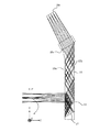
アイグラスディスプレイの外観は、図1に示すとおりである。図1において符号1で示すのがコンバイナ光学系である。コンバイナ光学系1の断面の概略は図2に示すとおりである。
Hereinafter, embodiments of the present invention will be described with reference to FIGS. 1, 2, and 3.
In the present embodiment, a combiner
First, the configuration of the combiner
The appearance of the eyeglass display is as shown in FIG. In FIG. 1,
図1,図2に示すように、コンバイナ光学系1は、アイグラスディスプレイにおいて光源ユニット3の画像表示面20aから射出した表示光束を使用者の眼の瞳の方向に導く。なお、図1中、符号16で示すのは、アイグラスディスプレイを使用者の頭部に装着するための装着具である。
図1,図2中に示す右手系のXYZ座標の原点の位置が、使用者の瞳の中心の位置である。この瞳は、コンバイナ光学系1の射出瞳(アイポイントE.P.)でもある。なお、図1,図2に示すようにXYZ座標系のZ軸は使用者の眼の視軸方向、Y軸は使用者の左右方向、X軸は使用者の上下方向とした。
As shown in FIGS. 1 and 2, the combiner
The position of the origin of the right-handed XYZ coordinates shown in FIGS. 1 and 2 is the position of the center of the user's pupil. This pupil is also the exit pupil (eye point EP) of the combiner
コンバイナ光学系1は、平行基板15を備える。また、その基板15内に、主反射面17、偏光ビームスプリッタ(PBS)13、及び1/4波長板14などを備える。
基板15は、その外縁が眼鏡レンズようなサイズ及び形状に整えられており、使用者の眼に正対して配置される。
画像表示面20aは、使用者の眼から十分に離れた位置に配置される。画像表示面20aから射出する表示光束の波長は可視光の所定の波長に設定されており、表示光束の偏光方向は、予めp偏光に整えられている。
The combiner
The outer edge of the
The
基板15の材料は、少なくともこの所定波長の可視光に対し透明な材料からなる。軽量化のために、光学用樹脂の使用が望ましい。
画像表示面20aの各位置から発散する表示光束の角度範囲は、適度に制限されている。これは、例えば、画像表示面20aを照明する照明光として、予め十分にコリメート(平行光束化)されたものを使用することで実現できる。
The material of the
The angle range of the display light beam that diverges from each position on the
PBS13は、使用者の眼の前方に傾斜した姿勢で設けられる。PBS13が基板15の使用者側の面15a又は外界側の面15bと成す角度θは、20°以上かつ40°以下である。
PBS13は、前記所定波長を選択波長として反射し、かつそれ以外の波長の可視光を反射しないような反射波長選択性を有している。
The PBS 13 is provided in a posture inclined in front of the user's eyes. The angle θ formed by the
The
画像表示面20aの配置位置及び配置角度は、画像表示面20aから射出した表示光束が基板15の使用者側の面15a及び外界側の面15bにて交互に内面反射して折線状の光路を基板15内に形成し、かつその光路とPBS13との成す角度が適正値になるよるよう選定される。
基板15において画像表示面20aから射出した表示光束が最初に入射する領域(境界面)15cは、光線の結像に対して非対称な要素が存在することを避けるため、画像表示面20aの中心から射出した表示光束の主光線に対し略垂直な平面となっている。
The arrangement position and the arrangement angle of the
The region (boundary surface) 15c where the display light beam emitted from the
主反射面17は、PBS13を透過した表示光束を反射できる位置に設けられる。
主反射面17は、その表示光束に対し光学的パワーを付与するための曲率又は回折パターンを有している。
主反射面17の姿勢は、画像表示面20aの中心から射出した表示光束の主光線がその主反射面17に対し垂直に入射するような姿勢に設定される。
The
The
The posture of the
1/4波長板14は、PBS13と主反射面17との間の表示光束の光路(主反射面17のなるべく近く)に挿入される。
次に、このコンバイナ光学系1内の光の振る舞いについて説明する。
画像表示面20aから射出したp偏光の表示光束は、基板15内を内面反射してからPBS13に入射し、PBS13を透過し、1/4波長板14を通過し、主反射面17に入射する。主反射面17における反射により表示光束は平行光束に近づけられつつ、1/4波長板14を再度通過し、PBS13に再入射する。
The quarter-
Next, the behavior of light in the combiner
The p-polarized display light beam emitted from the
1/4波長板14を往復した表示光束はs偏光となるので、PBS13に再入射した表示光束は、PBS13で反射される。また、表示光束の光路がPBS13と成す角度は適正値なので、PBS13で反射された表示光束は、使用者の眼の方向に進行し、平行光束に近い状態で眼の瞳に入射する。
よって、画像表示面20aの拡大虚像がPBS13の外界側に形成される。この状態で、使用者には、画像表示面20aが眼の前方にあるように見える。また、PBS13は外界から入射する外光の殆どを透過するので、観察者には、虚像と共に外界を見ることもできる。
Since the display light beam reciprocating the quarter-
Therefore, an enlarged virtual image of the
次に、このコンバイナ光学系1の効果について説明する。
先ず、使用者の眼の視軸(Z軸)上に配置される光学素子は、基板15、基板15内のPBSのみであり、従来例よりも少ない。
しかも、そのPBS13が基板15の使用者側の面15a又は外界側の面15bと成す角度θは40°以下であり、従来例のそれ(45°)よりも5°小さい。5°小さければ、基板15の使用者側の面15aと外界側の面15bとの間隔は確実に狭められる。
Next, the effect of this combiner
First, the optical elements arranged on the visual axis (Z-axis) of the user's eye are only the
Moreover, the angle θ between the
したがって、このコンバイナ光学系1の視軸方向(Z方向)の厚さは、従来例のそれよりも薄い。
また、PBS13と基板15の使用者側の面15a又は外界側の面15bとの成す角度θが20°以上であるので、基板15の内部に折線状の光路は適正に形成される。つまり、基板15の使用者側の面15a又は外界側の面15bのうち、表示光束をn回目に反射する領域と、n+1回目に反射する領域とを独立させる(重複させない)ことができる。
Therefore, the thickness of the combiner
In addition, since the angle θ formed by the
因みに、PBS13と基板15の使用者側の面15a又は外界側の面15bとの成す角度θが20°未満であると、光路を適正に形成することが難しくなる。
また、画像表示面20aの各位置から発散する光束の角度範囲が適度に制限されているので、迷光が抑えられ、虚像の近傍に迷光によるゴーストが生起する、といった事態を避けることができる。
Incidentally, when the angle θ formed by the
In addition, since the angular range of the light beam that diverges from each position on the
また、主反射面17の姿勢は、画像表示面20aの中心から射出した表示光束の主光線がその主反射面17に対し垂直に入射するような姿勢に設定されるので、前記虚像の結像収差は最小に抑えられる。
また、PBS13は、反射波長選択性を有し、表示光束と異なる波長の光については全て透過するので、コンバイナ光学系1のシースルー性(外光の透過性)は高い。
(その他)
なお、画像表示面20aの各位置から発散する光束の角度範囲を制限するために、照明光を使用するとしたが、その代わりにフィールドレンズを画像表示面20aの射出側に挿入してもよい。
Further, the posture of the
Further, the
(Other)
It should be noted that illumination light is used to limit the angle range of the light beam that diverges from each position on the
また、画像表示面20aには、LCDなどの透過又は反射式の二次元画像表示素子、ELなどの自発光式の二次元画像表示素子などが配置される。
また、画像表示面20aに直接二次元画像表示素子を配置せずに、二次元画像表示素子をリレー光学系により投影してできる中間像を配置してもよい。また、画像表示面20a上に、光走査による二次元画像を形成してもよい。
In addition, a transmissive or reflective two-dimensional image display element such as an LCD or a self-luminous two-dimensional image display element such as an EL is disposed on the
Further, instead of arranging the two-dimensional image display element directly on the
また、画像表示面20aの形状は、平面に限定されず、基板15の側に凸の球面であってもよい。
なお、基板15の境界面15cは、平面に限らず、凹又は凸の曲面であってもよい。各種収差が抑えやすくなるような形状に最適化されることが望ましい。
また、画像表示面20aと基板15との間に、追加レンズを挿入してもよい。追加レンズを挿入することにより、像面湾曲の制御、色収差の補正が容易となる。追加レンズは、基板15に接合されていても、基板15と分離されていてもよい。
Further, the shape of the
The
Further, an additional lens may be inserted between the
また、光量損失を許容するのであれば、PBS13に代えてBS(ビームスプリッタ)を備えると共に1/4波長板14を省略してもよい。このときには、表示光束を予めp偏光に整える必要は無い。
また、上述した反射波長選択性を有したPBS13は、GBO(Giant Birefringent Optics)膜からなる偏光分離膜、反射型ホログラムからなる偏光分離膜、光学多層膜からなる偏光分離膜、ワイヤーグリッド構造の偏光分離膜などによって実現できる。
If the loss of light amount is allowed, a BS (beam splitter) may be provided instead of the
In addition, the
因みに、ホログラムからなる偏光分離膜の製造時、反射波長帯域を制御するために、照射光波長又は照射光角度を僅かにずらした多重露光を適用してもよい。
また、コンバイナ光学系1のシースルー性を高める必要が無いときには、PBS13に対し反射波長選択性を付与する必要は無い。反射波長選択性の無いPBS13は、アルミニウムなどからなる偏光分離膜によって容易に実現できる。
Incidentally, in manufacturing a polarization separation film made of a hologram, in order to control the reflection wavelength band, multiple exposure in which the irradiation light wavelength or irradiation light angle is slightly shifted may be applied.
Further, when there is no need to increase the see-through property of the combiner
また、主反射面17は、金属膜、誘電体膜、反射型ホログラムなどによって実現できる。
また、PBS13と主反射面17との位置関係については、図2に示すものの他、図3に示すようにしてもよい。
図2の主反射面17は、PBS13を透過した後に基板15の使用者側の面15aにて一回反射した表示光束を反射するのに対し、図3の主反射面17は、PBS13を透過した表示光束を直接、反射する。
The
The positional relationship between the
The
また、主反射面17の形成位置は、基板15の内部に限らず、基板15の端面であってもよい。
Further, the formation position of the
以下、本発明の第1実施例を示す。
本実施例のコンバイナ光学系の光路図は、図4のとおりである。なお、図4では、光路に作用しない面については一部省略してある。また、図4の各要素には、実施形態においてそれに対応する要素と同じ符号を付した(図6,図8,図10,図12においても同様。)。
The first embodiment of the present invention will be described below.
The optical path diagram of the combiner optical system of the present embodiment is as shown in FIG. In FIG. 4, some surfaces that do not act on the optical path are omitted. Also, each element in FIG. 4 is assigned the same reference numeral as the corresponding element in the embodiment (the same applies to FIGS. 6, 8, 10, and 12).
このコンバイナ光学系のデータは、表1、表2のとおりである。 The data of this combiner optical system is as shown in Tables 1 and 2.

このコンバイナ光学系の収差図は、図5のとおりである。
なお、図5に示す収差図は、横収差図である。図5において、「Y−FAN」はY方向の横収差図、「X−FAN」はX方向の横収差図である。また、中央の座標(X°,Y°)は、画角である(図7,図9,図11においても同様)。
The aberration diagram of this combiner optical system is as shown in FIG.
The aberration diagram shown in FIG. 5 is a lateral aberration diagram. In FIG. 5, “Y-FAN” is a lateral aberration diagram in the Y direction, and “X-FAN” is a lateral aberration diagram in the X direction. The central coordinates (X °, Y °) are the angles of view (the same applies to FIGS. 7, 9, and 11).
以下、本発明の第2実施例を示す。
本実施例のコンバイナ光学系の光路図は、図6のとおりである。なお、図6では、光路に作用しない面については一部省略してある。
このコンバイナ光学系のデータは、表3、表4のとおりである。
The second embodiment of the present invention will be described below.
The optical path diagram of the combiner optical system of the present embodiment is as shown in FIG. In FIG. 6, some surfaces that do not act on the optical path are omitted.
The data of this combiner optical system is as shown in Tables 3 and 4.
以下、本発明の第3実施例を示す。
本実施例のコンバイナ光学系の光路図は、図8のとおりである。なお、図8では、光路に作用しない面については一部省略してある。
このコンバイナ光学系のデータは、表5、表6のとおりである。
The third embodiment of the present invention will be described below.
The optical path diagram of the combiner optical system of this example is as shown in FIG. In FIG. 8, some surfaces that do not act on the optical path are omitted.
The data of this combiner optical system are as shown in Tables 5 and 6.
以下、本発明の第4実施例を示す。
本実施例のコンバイナ光学系の光路図は、図10のとおりである。なお、図10では、光路に作用しない面については一部省略してある。
このコンバイナ光学系のデータは、表7、表8のとおりである。
The fourth embodiment of the present invention will be described below.
The optical path diagram of the combiner optical system of this example is as shown in FIG. In FIG. 10, some surfaces that do not act on the optical path are omitted.
The data of this combiner optical system are as shown in Tables 7 and 8.
以下、本発明の第5実施例を示す。
本実施例のコンバイナ光学系の光路図は、図12のとおりである。なお、図12では、光路に作用しない面については一部省略してある。
このコンバイナ光学系のデータは、表9、表10のとおりである。
The fifth embodiment of the present invention will be described below.
The optical path diagram of the combiner optical system of the present embodiment is as shown in FIG. In FIG. 12, some surfaces that do not act on the optical path are omitted.
The data of this combiner optical system are as shown in Table 9 and Table 10.
1 コンバイナ光学系
20a 画像表示面
13 ビームスプリッタ(BS)、偏光ビームスプリッタ(PBS)
14 1/4波長板
15 基板
15a 使用者側の面
15b 外界側の面
15c 境界面
17 主反射面
E.P. 射出瞳(アイポイント)
1 Combiner
14 1/4
Claims (5)
前記基板内に形成される前記光路中に挿入されたビームスプリッタと、
前記ビームスプリッタを透過した前記表示光束に対し光学的パワーを付与すると共に、その表示光束が前記ビームスプリッタに再入射する方向にその表示光束を反射する主反射面とを備え、
前記ビームスプリッタが前記基板の表面と成す角度は、20°以上かつ40°以下である
ことを特徴とするコンバイナ光学系。 A transparent substrate that internally forms an optical path of a display light beam introduced from the image display surface;
A beam splitter inserted into the optical path formed in the substrate;
The optical power is applied to the display light beam transmitted through the beam splitter, and a main reflection surface that reflects the display light beam in a direction in which the display light beam re-enters the beam splitter,
An angle formed by the beam splitter and the surface of the substrate is 20 ° or more and 40 ° or less.
前記主反射面は、前記画像表示面の中心から射出した前記表示光束の主光線に対し垂直である
ことを特徴とするコンバイナ光学系。 The combiner optical system according to claim 1,
The combiner optical system, wherein the main reflection surface is perpendicular to a principal ray of the display light beam emitted from the center of the image display surface.
前記ビームスプリッタは、偏光ビームスプリッタであり、
前記ビームスプリッタと前記主反射面との間の前記表示光束の光路には、1/4波長板が挿入される
ことを特徴とするコンバイナ光学系。 The combiner optical system according to claim 1 or 2,
The beam splitter is a polarizing beam splitter;
A combiner optical system, wherein a quarter-wave plate is inserted in an optical path of the display light beam between the beam splitter and the main reflection surface.
前記偏光ビームスプリッタは、前記表示光束の波長を選択波長とした反射波長選択性を有している
ことを特徴とするコンバイナ光学系。 The combiner optical system according to claim 3,
The combiner optical system, wherein the polarization beam splitter has a reflection wavelength selectivity with a wavelength of the display light beam as a selection wavelength.
前記偏光ビームスプリッタは、反射型ホログラムからなる
ことを特徴とするコンバイナ光学系。 The combiner optical system according to claim 4,
The combiner optical system, wherein the polarization beam splitter is made of a reflection hologram.
Priority Applications (1)
| Application Number | Priority Date | Filing Date | Title |
|---|---|---|---|
| JP2003318507A JP2005084522A (en) | 2003-09-10 | 2003-09-10 | Combiner optical system |
Applications Claiming Priority (1)
| Application Number | Priority Date | Filing Date | Title |
|---|---|---|---|
| JP2003318507A JP2005084522A (en) | 2003-09-10 | 2003-09-10 | Combiner optical system |
Publications (2)
| Publication Number | Publication Date |
|---|---|
| JP2005084522A true JP2005084522A (en) | 2005-03-31 |
| JP2005084522A5 JP2005084522A5 (en) | 2006-09-28 |
Family
ID=34417773
Family Applications (1)
| Application Number | Title | Priority Date | Filing Date |
|---|---|---|---|
| JP2003318507A Pending JP2005084522A (en) | 2003-09-10 | 2003-09-10 | Combiner optical system |
Country Status (1)
| Country | Link |
|---|---|
| JP (1) | JP2005084522A (en) |
Cited By (33)
| Publication number | Priority date | Publication date | Assignee | Title |
|---|---|---|---|---|
| JP2009031708A (en) * | 2007-06-26 | 2009-02-12 | Nikon Corp | Combiner optical system, wearable display device and eyeglasses |
| JP2009515225A (en) * | 2005-11-08 | 2009-04-09 | ラマス リミテッド | Polarization optics |
| JP2010230701A (en) * | 2009-03-25 | 2010-10-14 | Olympus Corp | Eyeglass-mounted type image display device |
| JP2011186332A (en) * | 2010-03-10 | 2011-09-22 | Shimadzu Corp | Display device |
| JP2016504627A (en) * | 2012-12-19 | 2016-02-12 | マイクロソフト テクノロジー ライセンシング,エルエルシー | Tiling of multiple holograms in waveguide displays. |
| JP2016541018A (en) * | 2013-11-22 | 2016-12-28 | カール・ツァイス・スマート・オプティクス・ゲゼルシャフト・ミット・ベシュレンクテル・ハフツングCarl Zeiss Smart Optics GmbH | Imaging optical system and display device having the imaging optical system |
| KR20180059434A (en) * | 2015-09-25 | 2018-06-04 | 투즈 테크놀로지스 게엠베하 | An imaging optical unit and a display device including such an imaging optical unit |
| US10048499B2 (en) | 2005-11-08 | 2018-08-14 | Lumus Ltd. | Polarizing optical system |
| US10302835B2 (en) | 2017-02-22 | 2019-05-28 | Lumus Ltd. | Light guide optical assembly |
| US10437031B2 (en) | 2016-11-08 | 2019-10-08 | Lumus Ltd. | Light-guide device with optical cutoff edge and corresponding production methods |
| US10481319B2 (en) | 2017-03-22 | 2019-11-19 | Lumus Ltd. | Overlapping facets |
| US10520731B2 (en) | 2014-11-11 | 2019-12-31 | Lumus Ltd. | Compact head-mounted display system protected by a hyperfine structure |
| US10551544B2 (en) | 2018-01-21 | 2020-02-04 | Lumus Ltd. | Light-guide optical element with multiple-axis internal aperture expansion |
| US10564417B2 (en) | 2016-10-09 | 2020-02-18 | Lumus Ltd. | Aperture multiplier using a rectangular waveguide |
| US10649214B2 (en) | 2005-02-10 | 2020-05-12 | Lumus Ltd. | Substrate-guide optical device |
| US10809528B2 (en) | 2014-04-23 | 2020-10-20 | Lumus Ltd. | Compact head-mounted display system |
| US10895679B2 (en) | 2017-04-06 | 2021-01-19 | Lumus Ltd. | Light-guide optical element and method of its manufacture |
| US11243434B2 (en) | 2017-07-19 | 2022-02-08 | Lumus Ltd. | LCOS illumination via LOE |
| US11262587B2 (en) | 2018-05-22 | 2022-03-01 | Lumus Ltd. | Optical system and method for improvement of light field uniformity |
| US11415812B2 (en) | 2018-06-26 | 2022-08-16 | Lumus Ltd. | Compact collimating optical device and system |
| US11448816B2 (en) | 2019-01-24 | 2022-09-20 | Lumus Ltd. | Optical systems including light-guide optical elements with two-dimensional expansion |
| US11523092B2 (en) | 2019-12-08 | 2022-12-06 | Lumus Ltd. | Optical systems with compact image projector |
| US11526003B2 (en) | 2018-05-23 | 2022-12-13 | Lumus Ltd. | Optical system including light-guide optical element with partially-reflective internal surfaces |
| US11543583B2 (en) | 2018-09-09 | 2023-01-03 | Lumus Ltd. | Optical systems including light-guide optical elements with two-dimensional expansion |
| US11561335B2 (en) | 2019-12-05 | 2023-01-24 | Lumus Ltd. | Light-guide optical element employing complementary coated partial reflectors, and light-guide optical element having reduced light scattering |
| US11630260B2 (en) | 2020-05-24 | 2023-04-18 | Lumus Ltd. | Production method and corresponding structures of compound light-guide optical elements |
| US11644676B2 (en) | 2020-09-11 | 2023-05-09 | Lumus Ltd. | Image projector coupled to a light guide optical element |
| US11789264B2 (en) | 2021-07-04 | 2023-10-17 | Lumus Ltd. | Display with stacked light-guide elements providing different parts of field of view |
| US11796729B2 (en) | 2021-02-25 | 2023-10-24 | Lumus Ltd. | Optical aperture multipliers having a rectangular waveguide |
| US11886008B2 (en) | 2021-08-23 | 2024-01-30 | Lumus Ltd. | Methods of fabrication of compound light-guide optical elements having embedded coupling-in reflectors |
| US11885966B2 (en) | 2019-12-30 | 2024-01-30 | Lumus Ltd. | Optical systems including light-guide optical elements with two-dimensional expansion |
| US11914161B2 (en) | 2019-06-27 | 2024-02-27 | Lumus Ltd. | Apparatus and methods for eye tracking based on eye imaging via light-guide optical element |
| US11914187B2 (en) | 2019-07-04 | 2024-02-27 | Lumus Ltd. | Image waveguide with symmetric beam multiplication |
Citations (2)
| Publication number | Priority date | Publication date | Assignee | Title |
|---|---|---|---|---|
| JP2000511306A (en) * | 1996-10-08 | 2000-08-29 | ザ マイクロオプティカル コーポレイション | Image combining system for eyeglasses and face mask |
| JP2000292745A (en) * | 1999-04-07 | 2000-10-20 | Minolta Co Ltd | Illuminating device and projection type display device |
-
2003
- 2003-09-10 JP JP2003318507A patent/JP2005084522A/en active Pending
Patent Citations (2)
| Publication number | Priority date | Publication date | Assignee | Title |
|---|---|---|---|---|
| JP2000511306A (en) * | 1996-10-08 | 2000-08-29 | ザ マイクロオプティカル コーポレイション | Image combining system for eyeglasses and face mask |
| JP2000292745A (en) * | 1999-04-07 | 2000-10-20 | Minolta Co Ltd | Illuminating device and projection type display device |
Cited By (48)
| Publication number | Priority date | Publication date | Assignee | Title |
|---|---|---|---|---|
| US10649214B2 (en) | 2005-02-10 | 2020-05-12 | Lumus Ltd. | Substrate-guide optical device |
| US10962784B2 (en) | 2005-02-10 | 2021-03-30 | Lumus Ltd. | Substrate-guide optical device |
| US10598937B2 (en) | 2005-11-08 | 2020-03-24 | Lumus Ltd. | Polarizing optical system |
| US10261321B2 (en) | 2005-11-08 | 2019-04-16 | Lumus Ltd. | Polarizing optical system |
| US9551880B2 (en) | 2005-11-08 | 2017-01-24 | Lumus Ltd. | Polarizing optical system |
| US10048499B2 (en) | 2005-11-08 | 2018-08-14 | Lumus Ltd. | Polarizing optical system |
| JP2009515225A (en) * | 2005-11-08 | 2009-04-09 | ラマス リミテッド | Polarization optics |
| JP2009031708A (en) * | 2007-06-26 | 2009-02-12 | Nikon Corp | Combiner optical system, wearable display device and eyeglasses |
| JP2010230701A (en) * | 2009-03-25 | 2010-10-14 | Olympus Corp | Eyeglass-mounted type image display device |
| JP2011186332A (en) * | 2010-03-10 | 2011-09-22 | Shimadzu Corp | Display device |
| JP2016504627A (en) * | 2012-12-19 | 2016-02-12 | マイクロソフト テクノロジー ライセンシング,エルエルシー | Tiling of multiple holograms in waveguide displays. |
| US10146053B2 (en) | 2012-12-19 | 2018-12-04 | Microsoft Technology Licensing, Llc | Multiplexed hologram tiling in a waveguide display |
| JP2016541018A (en) * | 2013-11-22 | 2016-12-28 | カール・ツァイス・スマート・オプティクス・ゲゼルシャフト・ミット・ベシュレンクテル・ハフツングCarl Zeiss Smart Optics GmbH | Imaging optical system and display device having the imaging optical system |
| US10809528B2 (en) | 2014-04-23 | 2020-10-20 | Lumus Ltd. | Compact head-mounted display system |
| US10908426B2 (en) | 2014-04-23 | 2021-02-02 | Lumus Ltd. | Compact head-mounted display system |
| US10782532B2 (en) | 2014-11-11 | 2020-09-22 | Lumus Ltd. | Compact head-mounted display system protected by a hyperfine structure |
| US10520731B2 (en) | 2014-11-11 | 2019-12-31 | Lumus Ltd. | Compact head-mounted display system protected by a hyperfine structure |
| JP2018529998A (en) * | 2015-09-25 | 2018-10-11 | トーツ・テクノロジーズ・ゲゼルシャフト・ミット・ベシュレンクテル・ハフツングTooz Technologies Gmbh | Imaging optical system and display device having the imaging optical system |
| KR20180059434A (en) * | 2015-09-25 | 2018-06-04 | 투즈 테크놀로지스 게엠베하 | An imaging optical unit and a display device including such an imaging optical unit |
| KR102618809B1 (en) * | 2015-09-25 | 2023-12-27 | 투즈 테크놀로지스 게엠베하 | Imaging optical unit and display device including such imaging optical unit |
| US10564417B2 (en) | 2016-10-09 | 2020-02-18 | Lumus Ltd. | Aperture multiplier using a rectangular waveguide |
| US11567316B2 (en) | 2016-10-09 | 2023-01-31 | Lumus Ltd. | Aperture multiplier with depolarizer |
| US11378791B2 (en) | 2016-11-08 | 2022-07-05 | Lumus Ltd. | Light-guide device with optical cutoff edge and corresponding production methods |
| US10437031B2 (en) | 2016-11-08 | 2019-10-08 | Lumus Ltd. | Light-guide device with optical cutoff edge and corresponding production methods |
| US10302835B2 (en) | 2017-02-22 | 2019-05-28 | Lumus Ltd. | Light guide optical assembly |
| US11194084B2 (en) | 2017-02-22 | 2021-12-07 | Lumus Ltd. | Light guide optical assembly |
| US10684403B2 (en) | 2017-02-22 | 2020-06-16 | Lumus Ltd. | Light guide optical assembly |
| US11125927B2 (en) | 2017-03-22 | 2021-09-21 | Lumus Ltd. | Overlapping facets |
| US10481319B2 (en) | 2017-03-22 | 2019-11-19 | Lumus Ltd. | Overlapping facets |
| US10895679B2 (en) | 2017-04-06 | 2021-01-19 | Lumus Ltd. | Light-guide optical element and method of its manufacture |
| US11243434B2 (en) | 2017-07-19 | 2022-02-08 | Lumus Ltd. | LCOS illumination via LOE |
| US11385393B2 (en) | 2018-01-21 | 2022-07-12 | Lumus Ltd. | Light-guide optical element with multiple-axis internal aperture expansion |
| US10551544B2 (en) | 2018-01-21 | 2020-02-04 | Lumus Ltd. | Light-guide optical element with multiple-axis internal aperture expansion |
| US11262587B2 (en) | 2018-05-22 | 2022-03-01 | Lumus Ltd. | Optical system and method for improvement of light field uniformity |
| US11526003B2 (en) | 2018-05-23 | 2022-12-13 | Lumus Ltd. | Optical system including light-guide optical element with partially-reflective internal surfaces |
| US11415812B2 (en) | 2018-06-26 | 2022-08-16 | Lumus Ltd. | Compact collimating optical device and system |
| US11543583B2 (en) | 2018-09-09 | 2023-01-03 | Lumus Ltd. | Optical systems including light-guide optical elements with two-dimensional expansion |
| US11448816B2 (en) | 2019-01-24 | 2022-09-20 | Lumus Ltd. | Optical systems including light-guide optical elements with two-dimensional expansion |
| US11914161B2 (en) | 2019-06-27 | 2024-02-27 | Lumus Ltd. | Apparatus and methods for eye tracking based on eye imaging via light-guide optical element |
| US11914187B2 (en) | 2019-07-04 | 2024-02-27 | Lumus Ltd. | Image waveguide with symmetric beam multiplication |
| US11561335B2 (en) | 2019-12-05 | 2023-01-24 | Lumus Ltd. | Light-guide optical element employing complementary coated partial reflectors, and light-guide optical element having reduced light scattering |
| US11523092B2 (en) | 2019-12-08 | 2022-12-06 | Lumus Ltd. | Optical systems with compact image projector |
| US11885966B2 (en) | 2019-12-30 | 2024-01-30 | Lumus Ltd. | Optical systems including light-guide optical elements with two-dimensional expansion |
| US11630260B2 (en) | 2020-05-24 | 2023-04-18 | Lumus Ltd. | Production method and corresponding structures of compound light-guide optical elements |
| US11644676B2 (en) | 2020-09-11 | 2023-05-09 | Lumus Ltd. | Image projector coupled to a light guide optical element |
| US11796729B2 (en) | 2021-02-25 | 2023-10-24 | Lumus Ltd. | Optical aperture multipliers having a rectangular waveguide |
| US11789264B2 (en) | 2021-07-04 | 2023-10-17 | Lumus Ltd. | Display with stacked light-guide elements providing different parts of field of view |
| US11886008B2 (en) | 2021-08-23 | 2024-01-30 | Lumus Ltd. | Methods of fabrication of compound light-guide optical elements having embedded coupling-in reflectors |
Similar Documents
| Publication | Publication Date | Title |
|---|---|---|
| JP2005084522A (en) | Combiner optical system | |
| CN105929535B (en) | Image display device | |
| US9733477B2 (en) | Dual axis internal optical beam tilt for eyepiece of an HMD | |
| US8848289B2 (en) | Near-to-eye display with diffractive lens | |
| US8035872B2 (en) | Image combiner and image display device | |
| EP2828703B1 (en) | Optical beam tilt for offset head mounted display | |
| JP6349704B2 (en) | Virtual image display device | |
| US9915823B1 (en) | Lightguide optical combiner for head wearable display | |
| US8294994B1 (en) | Image waveguide having non-parallel surfaces | |
| US7081999B2 (en) | Image display apparatus and head mounted display using it | |
| WO2016181459A1 (en) | Prism optical system, image display device using prism optical system, and imaging device using prism optical system | |
| JP2019505843A (en) | Wide-view personal display device | |
| JP5567924B2 (en) | Prism optical system, image display device using prism optical system, and imaging device using prism optical system | |
| JP2020095205A (en) | Image display device, and eyepiece optical system | |
| JP6812649B2 (en) | Image display device | |
| US20230023570A1 (en) | Near-eye optical system implementing a waveguide with an output viewer element having a refractive beam-splitting convex lens | |
| JP4194218B2 (en) | Image display device and image display system | |
| JP2018054977A (en) | Virtual image display device | |
| JP3524569B2 (en) | Visual display device | |
| JP7027748B2 (en) | Virtual image display device | |
| CN111443484B (en) | Virtual image display device | |
| JP2016170203A (en) | Image displaying apparatus | |
| JP4395673B2 (en) | Video display device | |
| US7675685B2 (en) | Image display apparatus | |
| US11281005B2 (en) | Compact head-mounted display system with orthogonal panels |
Legal Events
| Date | Code | Title | Description |
|---|---|---|---|
| A621 | Written request for application examination |
Free format text: JAPANESE INTERMEDIATE CODE: A621 Effective date: 20060705 |
|
| A521 | Written amendment |
Free format text: JAPANESE INTERMEDIATE CODE: A523 Effective date: 20060811 |
|
| A977 | Report on retrieval |
Free format text: JAPANESE INTERMEDIATE CODE: A971007 Effective date: 20090612 |
|
| A131 | Notification of reasons for refusal |
Free format text: JAPANESE INTERMEDIATE CODE: A131 Effective date: 20090623 |
|
| A521 | Written amendment |
Free format text: JAPANESE INTERMEDIATE CODE: A523 Effective date: 20090821 |
|
| A02 | Decision of refusal |
Free format text: JAPANESE INTERMEDIATE CODE: A02 Effective date: 20090915 |