JP2005039799A - Power amplifier, power distributor, and power synthesizer - Google Patents
Power amplifier, power distributor, and power synthesizer Download PDFInfo
- Publication number
- JP2005039799A JP2005039799A JP2004178371A JP2004178371A JP2005039799A JP 2005039799 A JP2005039799 A JP 2005039799A JP 2004178371 A JP2004178371 A JP 2004178371A JP 2004178371 A JP2004178371 A JP 2004178371A JP 2005039799 A JP2005039799 A JP 2005039799A
- Authority
- JP
- Japan
- Prior art keywords
- signal
- distributed constant
- line
- constant line
- wavelength
- Prior art date
- Legal status (The legal status is an assumption and is not a legal conclusion. Google has not performed a legal analysis and makes no representation as to the accuracy of the status listed.)
- Withdrawn
Links
Images


Landscapes
- Microwave Amplifiers (AREA)
- Amplifiers (AREA)
Abstract
Description
本発明は、高周波電力増幅器に関し、より特定的には、プッシュプル型の高周波電力増幅器およびそれに用いられる電力分配器および電力合成器に関する。 The present invention relates to a high frequency power amplifier, and more particularly to a push-pull type high frequency power amplifier, and a power distributor and power combiner used therefor.
図6は、従来のプッシュプル型の高周波電力増幅器の構成を示す図である。図6において、従来の電力増幅器9は、入力端子900と、バラン/整合回路901と、同一規格の電界効果トランジスタ(以下、FETという)902a,902bと、FET902a,902bのドレインに接続されたインダクタ903a,903bと、出力端子904と、出力端子904とFET902aのドレインとの間に接続された分布定数線路905と、分布定数線路905とFET902aのドレインとの間に並列に接続された直列共振回路906aと、出力端子904とFET902bのドレインとの間に並列に接続された直列共振回路906bとを含む。
FIG. 6 is a diagram showing a configuration of a conventional push-pull type high frequency power amplifier. In FIG. 6, a
バラン/整合回路901は、入力端子900に入力される基本波の位相を回転させ、互いに逆相の基本波成分を有する第1および第2の信号を出力する。第1および第2の信号は、それぞれFET902a,902bによって増幅される。ここで、基本波の波長をλとする。分布定数線路905の長さは、基本波の1/2波長(λ/2)の長さとなっている。FET902aから出力された信号は、分布定数線路905によって基本波成分の位相を180度回転させられ、FET902bから出力された信号と合成される。合成された信号は、出力端子904から出力される。
The balun /
基本波の周波数をfo(=1/λ)とした場合、直列共振回路906a,906bは、foの2倍の周波数2foで共振するように設定されている。したがって、増幅素子902a,902bで発生した互いに同相の2次高調波は、直列共振回路906a,906bにおいて短絡する。したがって、図6に示す従来の電力増幅器9は、2次歪みの発生を抑圧することができる。
When the frequency of the fundamental wave is fo (= 1 / λ), the
図7は、高調波に対するインピーダンスを考慮した整合回路を設けた従来のプッシュプル型の電力増幅器の構成を示す図である(特許文献1参照)。図7に示す従来の電力増幅器において、入力端子911に入力された基本波は、位相反転回路912によって、互いに逆相の二つの信号として出力され、それぞれ整合回路913,914を介して、FET915,916へ入力される。
FIG. 7 is a diagram showing a configuration of a conventional push-pull type power amplifier provided with a matching circuit in consideration of impedance with respect to harmonics (see Patent Document 1). In the conventional power amplifier shown in FIG. 7, the fundamental wave input to the input terminal 911 is output as two signals having opposite phases to each other by the phase inversion circuit 912, and the
FET915,916のドレインには、分布定数線路917,918が接続されている。分布定数線路917,918において、基本波の1/4波長の整数倍の長さL1の位置に、偶数次高調波に対して短絡となる基本波の1/4波長の長さL2となる一端を短絡したスタブ919,920が接続されている。
Distributed
また、分布定数線路917,918において、3次高調波に対して開放とするために基本波の1/12波長の長さL3の位置に、分布定数線路917と分布定数線路918とを結ぶコンデンサ921が接続されている。さらに、コンデンサ921の接続位置とスタブ919,920の接続位置との間の分布定数線路917,918において、基本波に対するインピーダンスの整合を取るために、コンデンサ922が接続されている。分布定数線路917,918からの信号は、位相反転器923で互いに同相の信号とされて合成され、出力端子924から出力される。
Further, in the distributed
図7に示す従来の電力増幅器において、FET915,916のゲート電圧をピッチオフ点に設定し、入力信号を十分振り込んだ場合、FETのドレイン電圧vdおよびドレイン電流idは、図8に示すような形状の波形となる。すなわち、ドレイン電圧vdは基本波と奇数次高調波成分からなる矩形波になり、ドレイン電流idは基本波と偶数次高調波からなる半波整流波形になる。したがって、電圧と電流とが同時に存在することがないため増幅素子内での電力消費がなくなるので、効率が100%になる。
図6に示した従来の電力増幅器では、2次高調波に対してインピーダンスを短絡とするために、直列共振回路906a,906bを一対のFETに対してそれぞれ設ける必要があった。
In the conventional power amplifier shown in FIG. 6, it is necessary to provide series
また、図7に示した従来の電力増幅器では、偶数次高調波に対してインピーダンスを短絡とするためのスタブ919,920を、一対のFETに対してそれぞれ設ける必要があった。
Further, in the conventional power amplifier shown in FIG. 7, it is necessary to provide
そのため、いずれの従来の電力増幅器においても、回路が大型化してしまうという問題があった。 Therefore, any conventional power amplifier has a problem that the circuit becomes large.
また、これら一対の直列共振回路やスタブは、それぞれが同じ特性である必要がある。しかし、増幅器を集積してモジュール化するような場合には、周辺部品の影響などにより一対の直列共振回路やスタブの高周波特性が微妙に異なることがある。これは、利得特性にばらつきを生じさせる原因となる。 The pair of series resonance circuits and stubs must have the same characteristics. However, when amplifiers are integrated and modularized, the high frequency characteristics of a pair of series resonant circuits and stubs may differ slightly due to the influence of peripheral components. This causes variations in the gain characteristics.
それゆえ、本発明の目的は、小型でかつ特性ばらつきの小さい高効率の電力増幅器を提供することである。さらに、本発明の他の目的は、このような電力増幅器で用いられる電力分配器および電力合成器を提供することである。 Therefore, an object of the present invention is to provide a high-efficiency power amplifier that is small in size and has little variation in characteristics. Furthermore, another object of the present invention is to provide a power distributor and a power combiner used in such a power amplifier.
上記課題を解決するために本発明は以下のような特徴を有する。本発明は、高周波信号を増幅するための電力増幅器であって、第1の信号を増幅するための第1の増幅素子と、第1の増幅素子とプッシュプル型に接続されており、第1の信号と逆相の第2の信号を増幅するための第2の増幅素子と、第1の増幅素子によって増幅された第1の信号における基本波成分の位相を反転させる線路長を有する第1の分布定数線路と、短絡させたい偶数次高調波成分の位相が反転する第1の分布定数線路上の位置と第2の増幅素子の出力側との間に接続され、短絡させたい偶数次高調波成分の周波数で直列共振する第1の共振回路と、第1の分布定数線路からの信号と第2の増幅素子からの信号とを合成して出力する出力端子とを備える。 In order to solve the above problems, the present invention has the following features. The present invention is a power amplifier for amplifying a high-frequency signal, and is connected to a first amplifying element for amplifying a first signal, a first amplifying element and a push-pull type, A first amplifier having a line length for inverting the phase of the fundamental component in the first signal amplified by the first amplifier, and a second amplifier for amplifying the second signal having a phase opposite to the first signal. Are connected between the position on the first distributed constant line where the phase of the even-order harmonic component to be short-circuited is inverted and the output side of the second amplifying element, and the even-order harmonic to be short-circuited. A first resonance circuit that resonates in series at the frequency of the wave component; and an output terminal that synthesizes and outputs the signal from the first distributed constant line and the signal from the second amplifying element.
本発明によれば、プッシュプル型の電力増幅器において、所望の偶数次高調波成分の周波数で直列共振し、かつ当該偶数次高調波の位相が反転する位置に接続されている一つの共振回路が、第1および第2の増幅素子で発生する偶数次高調波を相殺する。このように、1つの共振回路によって偶数次高調波歪みの発生を抑えることができるので、回路が小型化される電力増幅器を提供することができる。また、プッシュプル型の電力増幅器で用いられる二つの増幅素子毎に偶数次高調波歪みの発生を抑圧するための共振回路をそれぞれ設ける場合に比べ、特性ばらつきを低減することができる。 According to the present invention, in the push-pull type power amplifier, one resonant circuit that is connected in series at a frequency at which the frequency of the desired even-order harmonic component is inverted and the phase of the even-order harmonic is inverted is provided. The even-order harmonics generated in the first and second amplifying elements are canceled out. As described above, since the occurrence of even-order harmonic distortion can be suppressed by one resonance circuit, a power amplifier in which the circuit is miniaturized can be provided. In addition, characteristic variation can be reduced as compared with a case where a resonance circuit for suppressing generation of even harmonic distortion is provided for each of two amplification elements used in a push-pull type power amplifier.
好ましくは、第1の分布定数線路の線路長は、基本波の1/2波長であり、第1の共振回路を接続するための第1の分布定数線路上の位置は、第1の分布定数線路の端から基本波の1/4波長のところであり、第1の共振回路は、2次高調波の周波数で直列共振することを特徴とする。 Preferably, the line length of the first distributed constant line is ½ wavelength of the fundamental wave, and the position on the first distributed constant line for connecting the first resonant circuit is the first distributed constant. The first resonant circuit is in series resonance at the frequency of the second harmonic, being at a quarter wavelength of the fundamental wave from the end of the line.
これにより、第1の分布定数線路の線路長が基本波の1/2波長となるので、第1の信号における基本波の位相が180度回転する。また、第1の共振回路は、第1の分布定数線路の端から基本波の1/4波長のところ、すなわち2次高調波の1/2波長のところに接続されているので、第1の共振回路の両端において、2次高調波の位相は互いに反転している。さらに、第1の共振回路は、2次高調波の周波数で直列共振するので、2次高調波に対して短絡回路として働く。したがって、第1および第2の増幅素子の出力端において、2次高調波は相殺されることとなる。このように、各増幅素子の出力端に、個別に共振回路を設けなくとも、1つの共振回路によって構成される小型の電力増幅器が提供されることとなる。 Thereby, since the line length of the first distributed constant line is ½ wavelength of the fundamental wave, the phase of the fundamental wave in the first signal is rotated by 180 degrees. Further, since the first resonance circuit is connected from the end of the first distributed constant line to the quarter wavelength of the fundamental wave, that is, the half wavelength of the second harmonic, the first resonance circuit At both ends of the resonance circuit, the phases of the second harmonics are inverted from each other. Furthermore, the first resonant circuit resonates in series at the frequency of the second harmonic, and thus acts as a short circuit for the second harmonic. Therefore, the second harmonic is canceled at the output ends of the first and second amplifying elements. In this way, a small power amplifier constituted by one resonance circuit is provided without providing a resonance circuit individually at the output end of each amplification element.
好ましくは、第1の共振回路は、インダクタおよびコンデンサが対称に配置された直列共振回路であるとよい。これにより、第1の共振回路の両端から見たときのインピーダンスのずれを防止することができる。 Preferably, the first resonance circuit is a series resonance circuit in which inductors and capacitors are arranged symmetrically. Thereby, it is possible to prevent a shift in impedance when viewed from both ends of the first resonance circuit.
好ましくは、第1の共振回路は、短絡させたい偶数次高調波成分の波長の1/2の電気長を有する分布定数線路であるとよい。これにより、第1の共振回路の両端から見たときのインピーダンスのずれ防止できると共に、素子点数を低減することができる。 Preferably, the first resonance circuit is a distributed constant line having an electrical length that is ½ of the wavelength of the even-order harmonic component to be short-circuited. As a result, it is possible to prevent a shift in impedance when viewed from both ends of the first resonance circuit and to reduce the number of elements.
好ましくは、第1および第2の信号をそれぞれ第1および第2の増幅素子に入力するための電力分配器をさらに備え、電力分配器は、入力される信号を二分配し、一方を第1の信号として第1の増幅素子に入力する分配手段と、分配手段からの他方の信号における基本波成分の位相を反転させる線路長を有し、当該位相を反転させた信号を第2の信号として第2の増幅素子に入力する第2の分布定数線路と、短絡させたい偶数次高調波成分の位相が反転する第2の分布定数線路上の位置と第2の増幅素子の入力側との間に接続され、短絡させたい偶数次高調波成分の周波数で直列共振する第2の共振回路とを含む。 Preferably, the power distributor further includes a power distributor for inputting the first and second signals to the first and second amplifying elements, respectively, and the power distributor divides the input signal into two, and one of the first and second signals is the first. Having a line length that inverts the phase of the fundamental wave component in the other signal from the distributing means, and the inverted signal as the second signal. Between the second distributed constant line input to the second amplifying element, the position on the second distributed constant line where the phase of the even-order harmonic component to be short-circuited is inverted, and the input side of the second amplifying element And a second resonance circuit that resonates in series at the frequency of the even-order harmonic component to be short-circuited.
これにより、偶数次高調波が短絡されている第1および第2の信号が入力されることとなる。第1および第2の信号を入力するための電力分配器では、所望の偶数次高調波成分の周波数で直列共振し、かつ当該偶数次高調波の位相が反転する位置に接続されている一つの共振回路が、第1および第2の増幅素子で発生する偶数次高調波を相殺する。このように、1つの共振回路によって偶数次高調波歪みの発生が抑えられている信号を入力することができるので、電力分配器が内蔵されている小型の電力増幅器を提供することができる。1つの共振回路を用いるので、特性ばらつきを低減することができる。 As a result, the first and second signals in which the even-order harmonics are short-circuited are input. In the power divider for inputting the first and second signals, one of the power dividers connected in series at the frequency of the desired even-order harmonic component and the phase of the even-order harmonic is inverted. The resonance circuit cancels even-order harmonics generated in the first and second amplifying elements. As described above, since a signal in which the generation of even-order harmonic distortion is suppressed by one resonance circuit can be input, a small power amplifier with a built-in power distributor can be provided. Since one resonance circuit is used, characteristic variation can be reduced.
好ましくは、第2の分布定数線路の線路長は、基本波の1/2波長であり、第2の共振回路を接続するための第2の分布定数線路上の位置は、第2の分布定数線路の端から基本波の1/4波長のところであり、第2の共振回路は、2次高調波の周波数で直列共振することを特徴とする。 Preferably, the line length of the second distributed constant line is ½ wavelength of the fundamental wave, and the position on the second distributed constant line for connecting the second resonant circuit is the second distributed constant line. The second resonant circuit is in series resonance at the frequency of the second harmonic, being at a quarter wavelength of the fundamental wave from the end of the line.
これにより、第2の分布定数線路の線路長が基本波の1/2波長となるので、入力信号における基本波の位相が180度回転する。また、第2の共振回路は、第2の分布定数線路の端から基本波の1/4波長のところ、すなわち2次高調波の1/2波長のところに接続されているので、第2の共振回路の両端において、2次高調波の位相は互いに反転している。さらに、第2の共振回路は、2次高調波の周波数で直列共振するので、2次高調波に対して短絡回路として働く。したがって、第1および第2の増幅素子の入力端において、2次高調波は相殺されることとなり、2次高調波歪みの発生を抑圧する小型の電力増幅器が提供されることとなる。 As a result, the line length of the second distributed constant line becomes ½ wavelength of the fundamental wave, so that the phase of the fundamental wave in the input signal rotates 180 degrees. Further, since the second resonance circuit is connected from the end of the second distributed constant line to a quarter wavelength of the fundamental wave, that is, a half wavelength of the second harmonic, the second resonance circuit At both ends of the resonance circuit, the phases of the second harmonics are inverted from each other. Furthermore, since the second resonant circuit resonates in series at the frequency of the second harmonic, it acts as a short circuit for the second harmonic. Therefore, the second harmonics are canceled out at the input ends of the first and second amplifying elements, and a small power amplifier that suppresses the generation of the second harmonic distortion is provided.
好ましくは、第2の共振回路は、インダクタおよびコンデンサが対称に配置された直列共振回路であるとよい。これにより、第2の共振回路の両端から見たときのインピーダンスのずれを防止することができる。 Preferably, the second resonance circuit is a series resonance circuit in which inductors and capacitors are arranged symmetrically. As a result, it is possible to prevent a deviation in impedance when viewed from both ends of the second resonance circuit.
好ましくは、第2の共振回路は、短絡させたい偶数次高調波成分の波長の1/2の電気長を有する分布定数線路であるとよい。これにより、第2の共振回路の両端から見たときのインピーダンスのずれ防止できると共に、素子点数を低減することができる。 Preferably, the second resonance circuit is a distributed constant line having an electrical length that is ½ of the wavelength of the even-order harmonic component to be short-circuited. As a result, it is possible to prevent a shift in impedance when viewed from both ends of the second resonance circuit and to reduce the number of elements.
また、本発明は、高周波信号を増幅するための電力増幅器であって、第1の信号、および第1の信号と逆相の第2の信号を出力する電力分配器と、第1の信号を増幅するための第1の増幅素子と、第1の増幅素子とプッシュプル型に接続されており、第2の信号を増幅するための第2の増幅素子と、第1の増幅素子によって増幅された第1の信号における基本波成分の位相を反転させて、当該位相を反転させた第1の信号と第2の増幅素子によって増幅された第2の信号と合成して出力する電力合成器とを備え、電力分配器は、入力される信号を二分配し、一方を第1の信号として第1の増幅素子に入力する分配手段と、分配手段からの他方の信号における基本波成分の位相を反転させる線路長を有し、当該位相を反転させた信号を第2の信号として第2の増幅素子に入力する分布定数線路と、短絡させたい偶数次高調波成分の位相が反転する分布定数線路上の位置と第2の増幅素子の入力側との間に接続され、短絡させたい偶数次高調波成分の周波数で直列共振する共振回路とを含む。 The present invention also provides a power amplifier for amplifying a high-frequency signal, a power distributor that outputs a first signal and a second signal having a phase opposite to the first signal, and a first signal A first amplifying element for amplifying, a first amplifying element connected to the first amplifying element in a push-pull manner, a second amplifying element for amplifying the second signal, and amplified by the first amplifying element A power combiner that inverts the phase of the fundamental component in the first signal, combines the first signal with the inverted phase and the second signal amplified by the second amplifying element, and outputs the resultant signal; The power distributor divides the input signal into two, and distributes one of the signals as a first signal to the first amplifying element, and the phase of the fundamental component in the other signal from the distributing means A signal having a line length to be inverted and having the phase inverted is a second signal. Are connected between the distributed constant line input to the second amplifying element and the position on the distributed constant line where the phase of the even-order harmonic component to be short-circuited is inverted and the input side of the second amplifying element. And a resonance circuit that resonates in series at the frequency of the even-order harmonic component to be generated.
これにより、偶数次高調波歪みの発生を抑圧する電力分配器が内蔵された電力増幅器が提供されることとなる。 As a result, a power amplifier incorporating a power distributor that suppresses the occurrence of even-order harmonic distortion is provided.
好ましくは、分布定数線路の線路長は、基本波の1/2波長であり、共振回路を接続するための分布定数線路上の位置は、分布定数線路の端から基本波の1/4波長のところであり、共振回路は、2次高調波の周波数で直列共振するとよい。これにより、2次高調波歪みの発生を抑圧する電力分配器が提供されることとなる。 Preferably, the line length of the distributed constant line is ½ wavelength of the fundamental wave, and the position on the distributed constant line for connecting the resonant circuit is ¼ wavelength of the fundamental wave from the end of the distributed constant line. By the way, the resonance circuit may be in series resonance at the frequency of the second harmonic. This provides a power distributor that suppresses the occurrence of second-order harmonic distortion.
好ましくは、共振回路は、インダクタおよびコンデンサが対称に配置された直列共振回路であるとよい。これにより、共振回路の両端から見たときのインピーダンスのずれを防止することができる。 Preferably, the resonance circuit is a series resonance circuit in which inductors and capacitors are arranged symmetrically. As a result, it is possible to prevent a deviation in impedance when viewed from both ends of the resonance circuit.
好ましくは、共振回路は、短絡させたい偶数次高調波成分の波長の1/2の電気長を有する分布定数線路であるとよい。これにより、共振回路の両端から見たときのインピーダンスのずれ防止できると共に、素子点数を低減することができる。 Preferably, the resonant circuit is a distributed constant line having an electrical length that is ½ of the wavelength of the even-order harmonic component to be short-circuited. As a result, it is possible to prevent a shift in impedance when viewed from both ends of the resonance circuit and to reduce the number of elements.
また、本発明は、入力信号を二分配するための電力分配器であって、入力信号の電力を二分配する分配手段と、分配手段によって二分配された一方の信号を、第1の信号として出力するための第1の出力端子と、分配手段によって二分配された他方の信号における基本波成分の位相を反転させる線路長を有し、当該位相を反転させた信号を第2の信号とするための分布定数線路と、分布定数線路からの第2の信号を出力するための第2の出力端子と、短絡させたい偶数次高調波成分の位相が反転する分布定数線路上の位置と第1の出力端子との間に接続され、短絡させたい偶数次高調波成分の周波数で直列共振する共振回路とを備える。 The present invention is also a power distributor for distributing an input signal into two, a distribution means for distributing the power of the input signal into two, and one of the signals distributed by the distribution means as a first signal. A first output terminal for output and a line length that inverts the phase of the fundamental wave component in the other signal that has been bi-distributed by the distributing means, and the signal with the phase inverted is defined as the second signal. A distributed constant line for output, a second output terminal for outputting a second signal from the distributed constant line, a position on the distributed constant line where the phase of the even harmonic component to be short-circuited is inverted, and the first And a resonance circuit that is in series resonance at a frequency of an even-order harmonic component that is desired to be short-circuited.
これにより、偶数次高調波歪みの発生を抑圧する電力分配器が提供されることとなる。 This provides a power distributor that suppresses the occurrence of even-order harmonic distortion.
好ましくは、分布定数線路の線路長は、基本波の1/2波長であり、共振回路を接続するための分布定数線路上の位置は、分布定数線路の端から基本波の1/4波長のところであり、共振回路は、2次高調波の周波数で直列共振することを特徴とする。 Preferably, the line length of the distributed constant line is ½ wavelength of the fundamental wave, and the position on the distributed constant line for connecting the resonant circuit is ¼ wavelength of the fundamental wave from the end of the distributed constant line. By the way, the resonance circuit is characterized in that it resonates in series at the frequency of the second harmonic.
これにより、2次高調波歪みの発生を抑圧する電力分配器が提供されることとなる。 This provides a power distributor that suppresses the occurrence of second-order harmonic distortion.
好ましくは、共振回路は、インダクタおよびコンデンサが対称に配置された直列共振回路であることとよい。これにより、共振回路の両端から見たときのインピーダンスのずれを防止することができる。 Preferably, the resonance circuit is a series resonance circuit in which inductors and capacitors are arranged symmetrically. As a result, it is possible to prevent a deviation in impedance when viewed from both ends of the resonance circuit.
好ましくは、共振回路は、前記短絡させたい偶数次高調波成分の波長の1/2の電気長を有する分布定数線路であるとよい。これにより、第1の共振回路の両端から見たときのインピーダンスのずれ防止できると共に、素子点数を低減することができる。 Preferably, the resonant circuit is a distributed constant line having an electrical length that is ½ of the wavelength of the even-order harmonic component to be short-circuited. As a result, it is possible to prevent a shift in impedance when viewed from both ends of the first resonance circuit and to reduce the number of elements.
また、本発明は、入力される第1の信号と第2の信号とを合成するための電力合成器であって、第1の信号を入力するための第1の入力端子と、第2の信号を入力するための第2の入力端子と、第2の入力端子からの第2の信号における基本波成分の位相を反転させる線路長を有する分布定数線路と、短絡させたい偶数次高調波成分の位相が反転する分布定数線路上の位置と第1の入力端子との間に接続され、短絡させたい偶数次高調波成分の周波数で直列共振する共振回路と、第1の入力端子からの第1の信号と、分布定数線路からの信号とを合成する合成手段とを備える。
The present invention is also a power combiner for combining the input first signal and the second signal, the first input terminal for inputting the first signal, and the second A second input terminal for inputting a signal, a distributed constant line having a line length for inverting the phase of the fundamental wave component in the second signal from the second input terminal, and an even-order harmonic component to be short-circuited A resonance circuit connected in series between the position on the distributed constant line where the phase of the first phase is inverted and the first input terminal and resonating in series at the frequency of the even-order harmonic component to be short-circuited, and from the
これにより、偶数次高調波歪みの発生を抑圧する電力合成器が提供されることとなる。 This provides a power combiner that suppresses the occurrence of even-order harmonic distortion.
好ましくは、分布定数線路の線路長は、基本波の1/2波長であり、共振回路を接続するための分布定数線路上の位置は、分布定数線路の端から基本波の1/4波長のところであり、共振回路は、2次高調波の周波数で直列共振することを特徴とする。 Preferably, the line length of the distributed constant line is ½ wavelength of the fundamental wave, and the position on the distributed constant line for connecting the resonant circuit is ¼ wavelength of the fundamental wave from the end of the distributed constant line. By the way, the resonance circuit is characterized in that it resonates in series at the frequency of the second harmonic.
これにより、2次高調波歪みの発生を抑圧する電力合成器が提供されることとなる。 This provides a power combiner that suppresses the occurrence of second-order harmonic distortion.
好ましくは、共振回路は、インダクタおよびコンデンサが対称に配置された直列共振回路であるとよい。これにより、第1の共振回路の両端から見たときのインピーダンスのずれを防止することができる。 Preferably, the resonance circuit is a series resonance circuit in which inductors and capacitors are arranged symmetrically. Thereby, it is possible to prevent a shift in impedance when viewed from both ends of the first resonance circuit.
好ましくは、共振回路は、前記短絡させたい偶数次高調波成分の波長の1/2の電気長を有する分布定数線路であるとよい。これにより、第1の共振回路の両端から見たときのインピーダンスのずれ防止できると共に、素子点数を低減することができる。 Preferably, the resonant circuit is a distributed constant line having an electrical length that is ½ of the wavelength of the even-order harmonic component to be short-circuited. As a result, it is possible to prevent a shift in impedance when viewed from both ends of the first resonance circuit and to reduce the number of elements.
本発明によれば、所望の偶数次高調波成分の周波数で直列共振し、かつ当該偶数次高調波の位相が反転する位置に接続されている一つの共振回路が、第1および第2の増幅素子で発生する偶数次高調波を相殺する。プッシュプル型の電力増幅器で用いられる二つの増幅素子毎に偶数次高調波歪みの発生を抑圧するための共振回路をそれぞれ設ける場合に比べ、一つの共振回路によって偶数次高調波歪みの発生を抑えることができるので、回路が小型化される電力増幅器、電力分配器および電力合成器を提供することができ、特性ばらつきを低減することができる。 According to the present invention, a single resonant circuit that is connected in series to the position where the phase of the even-order harmonic is inverted and that is in series resonance at the frequency of the desired even-order harmonic component is the first and second amplifications. The even harmonics generated in the element are canceled out. Suppresses the generation of even-order harmonic distortion with a single resonance circuit, compared to the case where a resonance circuit for suppressing the generation of even-order harmonic distortion is provided for each of the two amplifying elements used in a push-pull type power amplifier. Therefore, it is possible to provide a power amplifier, a power divider, and a power combiner in which a circuit is miniaturized, and characteristic variations can be reduced.
以下、本発明の実施形態について説明する。
(第1の実施形態)
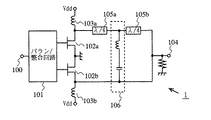
図1は、本発明の第1の実施形態に係る電力増幅器1の構成を示す図である。図1において、電力増幅器1は、入力端子100と、バラン/整合回路101と、第1の増幅素子102aと、第2の増幅素子102bと、第1の増幅素子102aのドレインに接続されたインダクタ103aと、第2の増幅素子102bのドレインに接続されたインダクタ103bと、出力端子104と、出力端子104と第1の増幅素子102aのドレインとの間に接続された分布定数線路105a,105bと、直列共振回路106とを含む。第1の増幅素子102aと第2の増幅素子102bとは、同一規格である。
Hereinafter, embodiments of the present invention will be described.
(First embodiment)
FIG. 1 is a diagram showing a configuration of a
直列共振回路106の一端は、分布定数線路105aと分布定数線路105bとの間に並列に接続されている。他端は、第2の増幅素子102bのドレインと出力端子104との間に並列に接続されている。直列共振回路106は、基本波の2次高調波の周波数で共振するように設定されている。
One end of the series
入力端子100に入力される信号における基本波成分の波長をλとする。分布定数線路105a,105bの長さは、基本波の1/4波長の長さ、すなわち、λ/4である。なお、図1では、説明を分かりやすくするために、分布定数線路105aと分布定数線路105bとの間が離れているように記載したが、実際は、二つの分布定数線路は、つながっており、基本波の1/2波長の長さの分布定数線路を構成している。直列共振回路106は、当該分布定数線路における第1の増幅素子102aのドレイン側から基本波の1/4波長の位置に、接続されている。
Let λ be the wavelength of the fundamental wave component in the signal input to the
バラン/整合回路101は、入力端子100に入力された基本波の位相を反転させて、互いに逆相の基本波成分を有する第1および第2の信号を出力する。第1および第2の増幅素子102a,102bは、バラン/整合回路101から出力される互いに逆相の二つの信号を増幅する。分布定数線路105aおよび分布定数線路105bによって、第1の増幅素子102aから出力された信号は、位相が180度回転させられ、第2の増幅素子102bから出力された信号と合波されて、出力端子104から出力される。
The balun /
第1および第2の増幅素子102a,102bで発生する2次高調波は互いに同相である。基本波の周波数をfoとした場合、2次高調波の波長λ2は、1/(2fo)となる。したがって、分布定数線路105aの線路長は、2次高調波に対して、1/2波長となる。よって、分布定数線路105aによって、2次高調波の位相は180度回転する。直列共振回路106は2次高調波の周波数で共振すると想定したので、分布定数線路105aによって180度位相が回転した2次高調波と第2の増幅素子102bから出力される2次高調波とは、互いに打ち消し合うこととなる。結果、電力増幅器1は、2次歪みを抑圧することができる。
Second harmonics generated in the first and
(第2の実施形態)
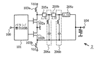
図2は、本発明の第2の実施形態に係る電力増幅器2の構成を示す図である。図2において、電力増幅器2は、入力端子100と、バラン/整合回路101と、第1の増幅素子102aと、第2の増幅素子102bと、第1の増幅素子102aのドレインに接続されたインダクタ103aと、第2の増幅素子102bのドレインに接続されたインダクタ103bと、出力端子104と、出力端子104と第1の増幅素子102aのドレインとの間に接続された分布定数線路205a,205b,205cと、直列共振回路206a,206bとを含む。なお、図2において、電力増幅器1と同一の部分については、図1に示したのと同一の参照符号を付し、説明を省略する。
(Second Embodiment)
FIG. 2 is a diagram showing a configuration of the
直列共振回路206aの一端は、分布定数線路205aと分布定数線路205bとの間に並列に接続されている。その他端は、第2の増幅素子102bのドレインと出力端子104との間に並列に接続されている。直列共振回路206aは、基本波の4次高調波の周波数で共振するように設定されている。
One end of the series
直列共振回路206bの一端は、分布定数線路205bと分布定数線路205cとの間に並列に接続されている。その他端は、第2の増幅素子102bのドレインと出力端子104との間に並列に接続されている。直列共振回路206bは、基本波の2次高調波の周波数で共振するように設定されている。
One end of the series
分布定数線路205a,205bの長さは、基本波の1/8波長の長さである。分布定数線路205cの長さは、基本波の1/4波長の長さである。なお、図2では、説明を分かりやすくするために、分布定数線路205a,205b,205cがそれぞれ離れているように記載したが、実際は、三つの分布定数線路は、つながっており、基本波の1/2波長の長さの分布定数線路を構成している。直列共振回路206aは、当該分布定数線路における第1の増幅素子102aのドレイン側から基本波の1/8波長の位置に、接続されている。また、直列共振回路206bは、当該分布定数線路における第1の増幅素子102aのドレイン側から基本波の1/4波長の位置に、接続されている。
The length of the distributed
分布定数線路205a,205b,205cで構成される分布定数線路によって、第1の増幅素子102aから出力された基本波は、位相が180度回転させられ、第2の増幅素子102bから出力された基本波と合波されて、出力端子104から出力される。
The fundamental wave output from the
また、分布定数線路205a,205bで構成される分布定数線路によって、2次高調波の位相は180度回転させられる。直列共振回路206bは2次高調波の周波数で共振するので、180度位相が回転した2次高調波と第2の増幅素子102bから出力される2次高調波とは、互いに打ち消し合うこととなる。結果、電力増幅器2は、2次高調波を打ち消すことができる。
Further, the phase of the second harmonic is rotated by 180 degrees by the distributed constant line composed of the distributed
さらに、分布定数線路205aによって、4次高調波の位相は180度回転させられる。直列共振回路206aは4次高調波の周波数で共振するので、180度位相が回転した4次高調波と第2の増幅素子102bから出力される4次高調波とは、互いに打ち消し合うこととなる。結果、電力増幅器2は、4次高調波を打ち消すことができる。
Further, the phase of the fourth harmonic is rotated 180 degrees by the distributed
図1および図2に示すように、本発明の実施形態に係る電力増幅器では、打ち消したい偶数次高調波を短絡させるための回路として、当該偶数次高調波の周波数で共振する直列共振回路が、分布定数線路の所定の位置に、一方の増幅素子の出力と他方の増幅素子の出力とをバイパスするように接続されている。これにより、偶数次高調波が直列共振回路で相殺されてしまうこととなるので、偶数次高調波歪みの発生を抑圧することができる。 As shown in FIGS. 1 and 2, in the power amplifier according to the embodiment of the present invention, as a circuit for short-circuiting even-order harmonics to be canceled, a series resonant circuit that resonates at the frequency of the even-order harmonics is Connected to a predetermined position of the distributed constant line so as to bypass the output of one amplifying element and the output of the other amplifying element. As a result, even-order harmonics are canceled out by the series resonance circuit, so that occurrence of even-order harmonic distortion can be suppressed.
なお、図1および図2に示すような直列共振回路を有する電力合成側の構成をバラン/整合回路内に設け、互いに逆相の基本波成分を有する第1および第2の信号を出力するようにしてもよい。 It is to be noted that a power combining side configuration having a series resonance circuit as shown in FIGS. 1 and 2 is provided in the balun / matching circuit so as to output first and second signals having fundamental wave components of opposite phases. It may be.
なお、図1および/または図2では、2次高調波および/または4次高調波を抑圧するための構成を示したが、その他の偶数次高調波を抑圧する場合にも同様の構成を取ることができる。具体的には、2n(nは自然数)次高調波を抑圧したい場合、分布定数線路における増幅端子の出力側から基本波の1/(4n)波長の位置に、相殺したい偶数次高調波の周波数で共振する直列共振回路を接続すればよい。 1 and / or 2 show the configuration for suppressing the second-order harmonic and / or the fourth-order harmonic, but the same configuration is adopted when other even-order harmonics are suppressed. be able to. Specifically, when it is desired to suppress the 2n (n is a natural number) order harmonic, the frequency of the even order harmonic to be canceled at the 1 / (4n) wavelength position of the fundamental wave from the output side of the amplification terminal in the distributed constant line. What is necessary is just to connect the series resonance circuit which resonates by.
なお、直列共振回路を接続する位置は、分布定数線路における増幅端子の出力側から基本波の1/(4n)波長の位置の他、分布定数線路における出力端子側から基本波の1/(4n)波長の位置であってもよい。 In addition to the position of the 1 / (4n) wavelength of the fundamental wave from the output side of the amplification terminal in the distributed constant line, the position where the series resonant circuit is connected is 1 / (4n of the fundamental wave from the output terminal side of the distributed constant line. ) It may be the position of the wavelength.
また、接続される直列共振回路は、少なくとも1つあれば所望の効果を得ることができる。 If at least one series resonant circuit is connected, a desired effect can be obtained.
なお、2次高調波の位相が反転するλ/4の位置では、2次高調波以外の偶数次高調波の位相も反転している。したがって、図1に示す電力増幅器1において、直列共振回路106が、2次高調波以外の偶数次高調波の波長でも直列共振するように、スタブを設けておけば、2次高調波以外の偶数次高調波も打ち消されることとなる。図2に示す場合も同様に、直列共振回路206aまたは206bが、2次高調波以外の偶数次高調波の波長でも直列共振するように、スタブを設けておけば、2次高調波以外の偶数次高調波も打ち消されることとなる。これにより所望の効果を得ることが期待できる。
In addition, at the position of λ / 4 where the phase of the second harmonic is inverted, the phase of the even harmonics other than the second harmonic is also inverted. Therefore, in the
(実施例)
以下、本発明の実施例について説明する。
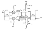
図3は、本発明の電力増幅器の実施例を示す回路図である。図3において、電力増幅器3は、入力端子301と、ゲートバイアス端子302と、ドレインバイアス端子303と、出力端子304と、入力結合コンデンサ311と、ゲートバイアスインダクタ312と、ドレインバイアスインダクタ313と、出力結合コンデンサ314と、第1のFET341と、第2のFET342と、合成端子351と、第1の分布定数線路352と、インダクタ361aと、コンデンサ362と、インダクタ361bと、分配端子321と、第2の分布定数線路322と、インダクタ331aと、コンデンサ332と、インダクタ331bとを含む。
(Example)
Examples of the present invention will be described below.
FIG. 3 is a circuit diagram showing an embodiment of the power amplifier of the present invention. 3, the
第1のFET341のソースと第2のFET342のソースとは、それぞれ接地されている。第1および第2のFET341,342は、第1の実施形態における第1および第2の増幅素子102a,102bに相当する(図1参照)。
The source of the
第2のFET342のドレインと合成端子351とは接続されている。第1のFET341のドレインと合成端子351との間には、第1の分布定数線路352が接続されている。第1の分布定数線路352は、基本波の1/2波長の長さの線路である。第1の分布定数線路352において第1のFET341のゲート側から基本波の1/4波長の長さの位置に、直列に接続されたインダクタ361b、コンデンサ362、およびインダクタ361aが、並列に接続される。インダクタ361aの一端は、合成端子351と第2のFET342のドレインとの間に並列に接続される。
The drain of the
インダクタ361a、コンデンサ362、およびインダクタ361bによって、第1の直列共振回路360が構成される。第1の直列共振回路360では、基本波の2倍の周波数で直列共振するように、インダクタ361a、コンデンサ362、およびインダクタ361bの値が設定されている。第1の直列共振回路360は、第1の実施形態における直列共振回路106に相当する(図1参照)。第1の直列共振回路360、第1の分布定数線路352、および合成端子351によって、電力合成器350が構成される。第1の直列共振回路360では、インダクタとコンデンサとが、LCLの関係になるように対称に接続されているので、第1の直列共振回路360の両端から見たときのインピーダンスが等しくなり、インピーダンスがずれることによるばらつきを防止することができる。なお、CLCの直列共振回路となるように、第1の直列共振回路360を構成してもよい。
The
合成端子351とドレインバイアス端子303との間には、ドレインバイアスインダクタ313が接続される。合成端子351と出力端子304との間には、出力結合コンデンサ314が接続される。
A
入力端子301と分配端子321との間には、入力結合コンデンサ311が接続されている。ゲートバイアス端子302と分配端子321との間には、ゲートバイアスインダクタ312が接続されている。
An
分配端子321と第2のFET342のゲートとの間には、第2の分布定数線路322が接続されている。分配端子321と第1のFET341のゲートとは接続されている。第2の分布定数線路322は、基本波の1/2波長の長さの線路である。第2の分布定数線路322において第2のFET342のゲート側から基本波の1/4波長の長さの位置に、直列に接続されたインダクタ331a、コンデンサ332、およびインダクタ331bが、並列に接続される。インダクタ331bの一端は、分配端子321と第1のFET341のゲートとの間に並列に接続される。
A second distributed
インダクタ331a、コンデンサ332、およびインダクタ331bによって、第2の直列共振回路330が構成される。第2の直列共振回路330において、基本波の2倍の周波数で直列共振するように、インダクタ331a、コンデンサ332、およびインダクタ331bの値が設定されている。第2の直列共振回路330、第2の分布定数線路322、および分配端子321によって、電力分配器320が構成される。電力分配器320は、第1の実施形態におけるバラン/整合回路101に相当する(図1参照)。第2の直列共振回路330では、インダクタとコンデンサとが、LCLの関係になるように対称に接続されているので、第2の直列共振回路330の両端から見たときのインピーダンスが等しくなり、インピーダンスがずれることによるばらつきを防止することができる。なお、CLCの直列共振回路となるように、第2の直列共振回路330を構成してもよい。
The
以下、図3に示す電力増幅器3の動作について説明する。
入力端子301に入力された基本波は、入力結合コンデンサ311を介して、電力分配器320の分配端子321に入力され、第1および第2の信号として分配される。分配端子321からの第2の入力信号は、基本波の1/2波長の長さを有する第2の分布定数線路322を介して、第2のFET342のゲートに入力される。分配端子321からの第1の信号は、第1のFET341のゲートに直接入力される。
Hereinafter, the operation of the
The fundamental wave input to the
第2の分布定数線路322によって、第2の信号における基本波成分および奇数次高調波成分の位相が180度回転する。したがって、第2のFET342のゲートに入力される信号と第1のFET341のゲートに入力される信号とは、基本波成分および奇数次高調波成分において逆位相となり、偶数次高調波成分において同相となる。なお、ゲ−トバイアスはゲートバイアス端子302からゲートバイアスインダクタ312を介して印加される。
By the second distributed
第2の直列共振回路330は、第2の分布定数線路322において第2のFET342のゲート側から基本波の1/4波長の長さの所、すなわち、2次高調波に対して1/2波長の長さの所に接続されている。したがって、第2の直列共振回路330と第2の分布定数線路322との接続点では、2次高調波の位相は180度回転していることとなるので、第2の直列共振回路330の両端における2次高調波は互いに逆相となる。第2の直列共振回路330は、2次高調波の周波数で直列共振し、短絡回路として働くので、2次高調波は相殺される。よって、第1のFET341および第2のFET342のゲート端では、2次高調波が存在しないこととなる。
The second series
第2のFET342で増幅された第2の信号は、合成端子351に入力される。一方、第1のFET341で増幅された第1の信号は、基本波の1/2波長の長さを有する第1の分布定数線路352を介して、合成端子351に入力される。第1の分布定数線路352によって、第1の入力信号における基本波成分および奇数次高調波成分の位相が180度回転する。したがって、合成端子351において、第2のFET342から出力される第2の信号と第1のFET341から出力される第1の信号とは、基本波成分および奇数次高調波成分において同相となる。なお、ドレインバイアスはドレインバイアス端子303からドレインバイアスインダクタ313を介して印加される。
The second signal amplified by the
第1の直列共振回路360は、第1の分布定数線路352において第1のFET341のドレイン側から基本波の1/4波長の長さの所、すなわち、2次高調波に対して1/2波長の長さの所に接続されている。したがって、第1の直列共振回路360と第1の分布定数線路352との接続点では、2次高調波の位相は180度回転している。第1の増幅素子341から出力される信号および第2の増幅素子342から出力される信号において、2次高調波は互いに同相であるので、第1の直列共振回路360の両端における2次高調波は互いに逆相となる。第1の直列共振回路360は、2次高調波の周波数で直列共振し、短絡回路として働くので、2次高調波は相殺される。よって、第1のFET341および第2のFET342のドレイン端では、2次高調波が存在しないこととなる。
The first
このように、図3に示す回路構成を有する電力増幅器では、二つのFETの入出力端で2次高調波が存在しないこととなるので、歪みが抑圧され、高い効率が得られることとなる。また、2次高調波を打ち消すための構成として、電力分配器側に一つの直列共振回路を設け、電力合成器側に一つの直列共振回路を設けるだけでよいので、小型化された電力増幅器が提供されることとなる。さらに、2次高調波を打ち消すための短絡回路として、電力分配器または電力合成器において、それぞれ一つの直列共振回路が用いられることとなるので、短絡回路のばらつきをなくすことができる。結果、パワー特性のばらつきが低減される電力増幅器が提供されることとなる。 In this way, in the power amplifier having the circuit configuration shown in FIG. 3, since the second harmonic does not exist at the input / output terminals of the two FETs, distortion is suppressed and high efficiency is obtained. In addition, as a configuration for canceling the second harmonic, it is only necessary to provide one series resonant circuit on the power distributor side and one series resonant circuit on the power combiner side. Will be provided. Further, since one series resonant circuit is used in each of the power distributor and the power combiner as a short circuit for canceling the second harmonic, variation in the short circuit can be eliminated. As a result, a power amplifier in which variations in power characteristics are reduced is provided.
なお、第1の直列共振回路360および/または第2の直列共振回路330は、分布定数回路であってもよい。図4は、第1の直列共振回路360および/または第2の直列共振回路330を分布定数線路400としたときの図を示す。図4において、第1の直列共振回路360および/または第2の直列共振回路330は、基本波の波長の1/4の電気長(2次高調波の波長の1/2の電気長)を有する分布定数線路400からなる。分布定数線路400の両端において、2次高調波は互いに逆相となるので、分布定数線路400の両端では、2次高調波は相殺される。
The first series
インダクタおよびコンデンサなどの受動素子から構成される直列共振回路が、高い周波数において、直列共振回路の両端で高調波のインピーダンスを完全に制御することは、困難である。しかし、分布定数線路からなる直列共振回路を用いることにより、高い周波数においても、分布定数線路その両端で高調波のインピーダンスを高い精度で容易に制御することができる。したがって、直列共振回路に分布定数線路を用いることによって、高い周波数においても、高調波成分を相殺することが可能となる。 It is difficult for a series resonant circuit composed of passive elements such as an inductor and a capacitor to completely control the harmonic impedance at both ends of the series resonant circuit at a high frequency. However, by using a series resonant circuit composed of distributed constant lines, it is possible to easily control the impedance of the harmonics at both ends of the distributed constant line with high accuracy even at high frequencies. Therefore, by using a distributed constant line in the series resonance circuit, it is possible to cancel harmonic components even at a high frequency.
また、図3に示すように、直列共振回路において、受動素子を対称に接続するのが好ましいが、対称な接続とすることによって、受動素子の素子点数が増加することとなる。しかし、分布定数線路を用いれば、両端から見たときのインピーダンスを等しくすることができるので、インピーダンスがずれることによるばらつきを防止することができ、かつ素子点数を低減することができる。 In addition, as shown in FIG. 3, in the series resonance circuit, it is preferable to connect the passive elements symmetrically. However, the symmetrical connection increases the number of elements of the passive elements. However, if the distributed constant line is used, the impedance when viewed from both ends can be made equal, so that variations due to the deviation of the impedance can be prevented and the number of elements can be reduced.
なお、図3に示す実施例では、電力分配器および電力合成器に2次高調波の短絡回路として直列共振回路を設けることとしたが、いずれか一方にのみ直列共振回路を設けることとしてもよい。 In the embodiment shown in FIG. 3, a series resonance circuit is provided as a second harmonic short circuit in the power distributor and the power combiner. However, a series resonance circuit may be provided only in one of them. .
なお、図3に示す電力分配器または電力合波回路は、それぞれ単独の部品として実施することができる。これらの部品は、プッシュプル型の電力増幅器に用いるものに限られない。 Note that the power distributor or the power combining circuit shown in FIG. 3 can be implemented as a single component. These components are not limited to those used in push-pull type power amplifiers.
なお、第1および第2の直列共振回路360,330は、2次高調波だけでなく、短絡させたい他の偶数次高調波に対しても同時に直列共振するように構成されていてもよい。これにより、2次高調波以外の偶数次高調波の発生を抑圧することができ、高効率化が図れる。
Note that the first and second
また、第1および第2の直列共振回路360,330の接続位置は、第1および第2の分布定数線路352,322のいずれかの端辺から偶数次高調波の1/2波長の長さの位置に接続されていてもよい。これにより、短絡させたい偶数次高調波の発生を抑圧することができる。
The connection position of the first and second
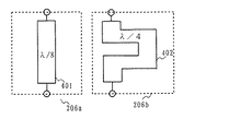
たとえば、2次高調波および4次高調波の発生を抑圧したい場合、各直列共振回路を分布定数線路とする構成を考える。図5は、2次高調波および4次高調波の発生を抑圧したい場合、各直列共振回路を分布定数線路とする構成を示す図である。基本波の波長の1/8の電気長(4次高調波の波長の1/2の電気長)を有する分布定数線路401は、図2に示す直列共振回路206aの役割を果たす。また、基本波の波長の1/4の電気長(2次高調波の波長の1/2の電気長)を有する分布定数線路402は、図2に示す直列共振回路206bの役割を果たす。このように、短絡させたい偶数次高調波に対して共振するような分布定数線路を図2に示すような受動素子を用いた直列共振回路の代わりに接続することで、偶数次高調波の発生を抑圧することができ、高効率化が図れる。ここで、短絡させたい偶数次高調波に対して共振するような分布定数線路の電気長は、短絡させたい偶数次高調波の波長の1/2の電気長となる。なお、図5に示すように、長い方の分布定数線路402は、折り曲げるなどして、短い方の分布定数線路401と端が一直線上に並ぶようにすればよい。また、分布定数線路同士を立体交差させるなどして、端が一直線上に並ぶようにしてもよい。同様のことが、その他の偶数次高調波についても言える。
For example, when it is desired to suppress the generation of the second harmonic and the fourth harmonic, consider a configuration in which each series resonance circuit is a distributed constant line. FIG. 5 is a diagram showing a configuration in which each series resonance circuit is used as a distributed constant line when generation of second harmonics and fourth harmonics is to be suppressed. A distributed
さらに、以上の構成に奇数次高調波を制御する回路を組み合わせれば、さらに高い効率が期待できる。 Furthermore, if a circuit that controls odd harmonics is combined with the above configuration, higher efficiency can be expected.
本発明にかかる電力増幅器、電力分配器および電力合成器は、小型でかつ特性ばらつきが小さく高効率であるので、通信機器等の分野において有用である。 The power amplifier, power divider, and power combiner according to the present invention are useful in the field of communication equipment and the like because they are small in size, have small variations in characteristics, and are highly efficient.
1,2,3, 電力増幅器
100,301 入力端子
101 バラン/整合回路
102a 第1の増幅素子
102b 第2の増幅素子
103a,103b インダクタ
104,304 出力端子
105a,105b,205a,205b,205c 分布定数線路
106,206a,206b 直列共振回路
321 分配端子
351 合成端子
341 第1のFET
342 第2のFET
352 第1の分布定数線路
322 第2の分布定数線路
360 第1の直列共振回路
330 第2の直列共振回路
320 電力分配器
350 電力合成器
302 ゲートバイアス端子
303 ドレインバイアス端子
311 入力結合コンデンサ
312 ゲートバイアスインダクタ
313 ドレインバイアスインダクタ
314 出力結合コンデンサ
331a,331b,361a,361b インダクタ
332,362 コンデンサ
400,401,402 分布定数線路
1, 2, 3,
342 second FET
352 First distributed
Claims (20)
第1の信号を増幅するための第1の増幅素子と、
前記第1の増幅素子とプッシュプル型に接続されており、前記第1の信号と逆相の第2の信号を増幅するための第2の増幅素子と、
前記第1の増幅素子によって増幅された前記第1の信号における基本波成分の位相を反転させる線路長を有する第1の分布定数線路と、
短絡させたい偶数次高調波成分の位相が反転する前記第1の分布定数線路上の位置と前記第2の増幅素子の出力側との間に接続され、前記短絡させたい偶数次高調波成分の周波数で直列共振する第1の共振回路と、
前記第1の分布定数線路からの信号と前記第2の増幅素子からの信号とを合成して出力する出力端子とを備える、電力増幅器。 A power amplifier for amplifying a high-frequency signal,
A first amplifying element for amplifying the first signal;
A second amplifying element connected to the first amplifying element in a push-pull manner for amplifying a second signal having a phase opposite to that of the first signal;
A first distributed constant line having a line length that inverts the phase of the fundamental component in the first signal amplified by the first amplification element;
Connected between the position on the first distributed constant line where the phase of the even-order harmonic component to be short-circuited is inverted and the output side of the second amplifying element, and the even-order harmonic component to be short-circuited A first resonant circuit in series resonance at a frequency;
A power amplifier comprising: an output terminal that combines and outputs a signal from the first distributed constant line and a signal from the second amplifying element.
前記電力分配器は、
入力される信号を二分配し、一方を前記第1の信号として前記第1の増幅素子に入力する分配手段と、
前記分配手段からの他方の信号における基本波成分の位相を反転させる線路長を有し、当該位相を反転させた信号を第2の信号として前記第2の増幅素子に入力する第2の分布定数線路と、
短絡させたい偶数次高調波成分の位相が反転する前記第2の分布定数線路上の位置と前記第2の増幅素子の入力側との間に接続され、前記短絡させたい偶数次高調波成分の周波数で直列共振する第2の共振回路とを含む、請求項1に記載の電力増幅器。 A power divider for inputting the first and second signals to the first and second amplifying elements, respectively;
The power distributor is
Distribution means for dividing an input signal into two and inputting one of the signals as the first signal to the first amplifying element;
A second distributed constant having a line length for inverting the phase of the fundamental component in the other signal from the distributing means and inputting the inverted signal to the second amplifying element as a second signal; Tracks,
Connected between the position on the second distributed constant line where the phase of the even-order harmonic component to be short-circuited is inverted and the input side of the second amplifying element, and the even-order harmonic component to be short-circuited The power amplifier according to claim 1, further comprising a second resonant circuit that resonates in series at a frequency.
第1の信号、および前記第1の信号と逆相の第2の信号を出力する電力分配器と、
前記第1の信号を増幅するための第1の増幅素子と、
前記第1の増幅素子とプッシュプル型に接続されており、前記第2の信号を増幅するための第2の増幅素子と、
前記第1の増幅素子によって増幅された前記第1の信号における基本波成分の位相を反転させて、当該位相を反転させた前記第1の信号と前記第2の増幅素子によって増幅された前記第2の信号と合成して出力する電力合成器とを備え、
前記電力分配器は、
入力される信号を二分配し、一方を前記第1の信号として前記第1の増幅素子に入力する分配手段と、
前記分配手段からの他方の信号における基本波成分の位相を反転させる線路長を有し、当該位相を反転させた信号を第2の信号として前記第2の増幅素子に入力する分布定数線路と、
短絡させたい偶数次高調波成分の位相が反転する前記分布定数線路上の位置と前記第2の増幅素子の入力側との間に接続され、前記短絡させたい偶数次高調波成分の周波数で直列共振する共振回路とを含む、電力増幅器。 A power amplifier for amplifying a high-frequency signal,
A power distributor that outputs a first signal and a second signal having a phase opposite to that of the first signal;
A first amplifying element for amplifying the first signal;
A second amplifying element connected to the first amplifying element in a push-pull manner for amplifying the second signal;
The phase of the fundamental component in the first signal amplified by the first amplifying element is inverted, and the first signal having the inverted phase and the second signal amplified by the second amplifying element are used. A power combiner that combines and outputs the two signals,
The power distributor is
Distribution means for dividing an input signal into two and inputting one of the signals as the first signal to the first amplifying element;
A distributed constant line that has a line length that inverts the phase of the fundamental wave component in the other signal from the distribution means, and that inputs the inverted signal to the second amplifying element as a second signal;
Connected between the position on the distributed constant line where the phase of the even-order harmonic component to be short-circuited is inverted and the input side of the second amplifying element, and in series at the frequency of the even-order harmonic component to be short-circuited A power amplifier including a resonant circuit that resonates.
前記入力信号の電力を二分配する分配手段と、
前記分配手段によって二分配された一方の信号を、第1の信号として出力するための第1の出力端子と、
前記分配手段によって二分配された他方の信号における基本波成分の位相を反転させる線路長を有し、当該位相を反転させた信号を第2の信号とするための分布定数線路と、
前記分布定数線路からの前記第2の信号を出力するための第2の出力端子と、
短絡させたい偶数次高調波成分の位相が反転する前記分布定数線路上の位置と前記第1の出力端子との間に接続され、前記短絡させたい偶数次高調波成分の周波数で直列共振する共振回路とを備える、電力分配器。 A power distributor for dividing an input signal into two parts,
A distribution means for distributing the power of the input signal into two;
A first output terminal for outputting one of the two signals distributed by the distributing means as a first signal;
A distributed constant line having a line length that inverts the phase of the fundamental component in the other signal that has been bipartively distributed by the distributing means, and the signal having the inverted phase as a second signal;
A second output terminal for outputting the second signal from the distributed constant line;
Resonance connected in series between the position on the distributed constant line where the phase of the even-order harmonic component to be short-circuited is inverted and the first output terminal, and in series resonance at the frequency of the even-order harmonic component to be short-circuited And a power distributor.
前記第1の信号を入力するための第1の入力端子と、
前記第2の信号を入力するための第2の入力端子と、
前記第2の入力端子からの前記第2の信号における基本波成分の位相を反転させる線路長を有する分布定数線路と、
短絡させたい偶数次高調波成分の位相が反転する前記分布定数線路上の位置と前記第1の入力端子との間に接続され、前記短絡させたい偶数次高調波成分の周波数で直列共振する共振回路と、
前記第1の入力端子からの前記第1の信号と、前記分布定数線路からの信号とを合成する合成手段とを備える、電力合成器。 A power combiner for combining an input first signal and a second signal,
A first input terminal for inputting the first signal;
A second input terminal for inputting the second signal;
A distributed constant line having a line length for inverting the phase of the fundamental component in the second signal from the second input terminal;
Resonance that is connected between the position on the distributed constant line where the phase of the even-order harmonic component to be short-circuited is inverted and the first input terminal, and series-resonates at the frequency of the even-order harmonic component to be short-circuited Circuit,
A power combiner comprising: a combining unit that combines the first signal from the first input terminal and the signal from the distributed constant line.
18. The power combiner according to claim 17, wherein the resonance circuit is a distributed constant line having an electrical length that is ½ of the wavelength of the even-order harmonic component to be short-circuited.
Priority Applications (1)
| Application Number | Priority Date | Filing Date | Title |
|---|---|---|---|
| JP2004178371A JP2005039799A (en) | 2003-06-26 | 2004-06-16 | Power amplifier, power distributor, and power synthesizer |
Applications Claiming Priority (2)
| Application Number | Priority Date | Filing Date | Title |
|---|---|---|---|
| JP2003183231 | 2003-06-26 | ||
| JP2004178371A JP2005039799A (en) | 2003-06-26 | 2004-06-16 | Power amplifier, power distributor, and power synthesizer |
Publications (2)
| Publication Number | Publication Date |
|---|---|
| JP2005039799A true JP2005039799A (en) | 2005-02-10 |
| JP2005039799A5 JP2005039799A5 (en) | 2007-07-26 |
Family
ID=34220319
Family Applications (1)
| Application Number | Title | Priority Date | Filing Date |
|---|---|---|---|
| JP2004178371A Withdrawn JP2005039799A (en) | 2003-06-26 | 2004-06-16 | Power amplifier, power distributor, and power synthesizer |
Country Status (1)
| Country | Link |
|---|---|
| JP (1) | JP2005039799A (en) |
Cited By (13)
| Publication number | Priority date | Publication date | Assignee | Title |
|---|---|---|---|---|
| JP2006287450A (en) * | 2005-03-31 | 2006-10-19 | Mitsubishi Heavy Ind Ltd | Harmonic suppression circuit and signal amplifier circuit |
| JP2009246871A (en) * | 2008-03-31 | 2009-10-22 | Mitsubishi Electric Corp | Second harmonic suppression circuit |
| JP2010011186A (en) * | 2008-06-27 | 2010-01-14 | Mitsubishi Electric Corp | Doherty amplifier |
| JP2011109525A (en) * | 2009-11-19 | 2011-06-02 | Fujitsu Semiconductor Ltd | Semiconductor device and radio communication apparatus |
| KR101060937B1 (en) | 2009-07-30 | 2011-08-30 | 삼성전기주식회사 | Push-Pull Broadband Power Amplifiers |
| US8476980B2 (en) | 2009-02-04 | 2013-07-02 | Nec Corporation | High frequency power amplifier |
| JP2013141291A (en) * | 2007-06-22 | 2013-07-18 | Cree Inc | Rf power transistor package accompanying harmonic frequency reduction inside and formation method of the same |
| JP2013187578A (en) * | 2012-03-06 | 2013-09-19 | Nec Corp | High frequency power amplification circuit |
| JP2013542700A (en) * | 2010-09-02 | 2013-11-21 | サムスン エレクトロニクス カンパニー リミテッド | RESONANT POWER TRANSMITTING SYSTEM POWER CONVERTER AND RESONANT POWER TRANSMITTING DEVICE |
| JP2013243748A (en) * | 2013-07-19 | 2013-12-05 | Spansion Llc | Semiconductor device and radio communication instrument |
| US9209760B2 (en) | 2013-03-14 | 2015-12-08 | Kabushiki Kaisha Toshiba | High-frequency, broadband amplifier circuit |
| JP2018519758A (en) * | 2015-06-30 | 2018-07-19 | トゥルンプフ ヒュッティンガー ゲゼルシャフト ミット ベシュレンクテル ハフツング ウント コンパニー コマンディートゲゼルシャフトTRUMPF Huettinger GmbH + Co. KG | High frequency amplifier device |
| CN108599734A (en) * | 2018-05-10 | 2018-09-28 | 南京信息工程大学 | Broadband active power splitter and broadband active power combiner |
-
2004
- 2004-06-16 JP JP2004178371A patent/JP2005039799A/en not_active Withdrawn
Cited By (15)
| Publication number | Priority date | Publication date | Assignee | Title |
|---|---|---|---|---|
| JP2006287450A (en) * | 2005-03-31 | 2006-10-19 | Mitsubishi Heavy Ind Ltd | Harmonic suppression circuit and signal amplifier circuit |
| JP4611081B2 (en) * | 2005-03-31 | 2011-01-12 | 三菱重工業株式会社 | Harmonic suppression circuit and signal amplification circuit |
| JP2013141291A (en) * | 2007-06-22 | 2013-07-18 | Cree Inc | Rf power transistor package accompanying harmonic frequency reduction inside and formation method of the same |
| JP2009246871A (en) * | 2008-03-31 | 2009-10-22 | Mitsubishi Electric Corp | Second harmonic suppression circuit |
| JP2010011186A (en) * | 2008-06-27 | 2010-01-14 | Mitsubishi Electric Corp | Doherty amplifier |
| US8476980B2 (en) | 2009-02-04 | 2013-07-02 | Nec Corporation | High frequency power amplifier |
| KR101060937B1 (en) | 2009-07-30 | 2011-08-30 | 삼성전기주식회사 | Push-Pull Broadband Power Amplifiers |
| JP2011109525A (en) * | 2009-11-19 | 2011-06-02 | Fujitsu Semiconductor Ltd | Semiconductor device and radio communication apparatus |
| JP2013542700A (en) * | 2010-09-02 | 2013-11-21 | サムスン エレクトロニクス カンパニー リミテッド | RESONANT POWER TRANSMITTING SYSTEM POWER CONVERTER AND RESONANT POWER TRANSMITTING DEVICE |
| US9553456B2 (en) | 2010-09-02 | 2017-01-24 | Samsung Electronics Co., Ltd. | Power converter in resonance power transmission system, and resonance power transmission apparatus |
| JP2013187578A (en) * | 2012-03-06 | 2013-09-19 | Nec Corp | High frequency power amplification circuit |
| US9209760B2 (en) | 2013-03-14 | 2015-12-08 | Kabushiki Kaisha Toshiba | High-frequency, broadband amplifier circuit |
| JP2013243748A (en) * | 2013-07-19 | 2013-12-05 | Spansion Llc | Semiconductor device and radio communication instrument |
| JP2018519758A (en) * | 2015-06-30 | 2018-07-19 | トゥルンプフ ヒュッティンガー ゲゼルシャフト ミット ベシュレンクテル ハフツング ウント コンパニー コマンディートゲゼルシャフトTRUMPF Huettinger GmbH + Co. KG | High frequency amplifier device |
| CN108599734A (en) * | 2018-05-10 | 2018-09-28 | 南京信息工程大学 | Broadband active power splitter and broadband active power combiner |
Similar Documents
| Publication | Publication Date | Title |
|---|---|---|
| JP6026062B1 (en) | Load modulation amplifier | |
| US20070205828A1 (en) | Switched mode power amplifier using lumped element impedance inverter for parallel combining | |
| WO2012160755A1 (en) | High-frequency amplifier circuit | |
| JPH11251849A (en) | High frequency power amplifier | |
| JP2005039799A (en) | Power amplifier, power distributor, and power synthesizer | |
| US8026775B2 (en) | Decade bandwidth planar MMIC four port transformer | |
| JP6729986B2 (en) | Doherty amplifier and Doherty amplifier circuit | |
| US6980057B2 (en) | Power amplifier, power distributor, and power combiner | |
| JP5646302B2 (en) | Frequency multiplier | |
| CN113824412A (en) | Differential amplifier circuit | |
| JP6482685B2 (en) | High frequency amplifier and amplifier module | |
| JP5516425B2 (en) | High frequency power amplifier | |
| JP2515963B2 (en) | High efficiency power amplifier | |
| JP2011176394A (en) | Power amplifier | |
| JP2005341447A (en) | High-frequency power amplifier | |
| JP2005260703A (en) | Power composite type amplifier | |
| KR20010091896A (en) | Power amplifier | |
| JP4293943B2 (en) | High frequency power amplifier | |
| JP2010268248A (en) | Ac power amplifier | |
| JP2007158648A (en) | Microwave amplifier | |
| JP2016076752A (en) | Push-pull power amplifier | |
| JPH0738350A (en) | Power amplifier | |
| JP5773364B2 (en) | EM class amplifier | |
| JPH02260905A (en) | High frequency power amplifier circuit | |
| US8854157B2 (en) | Balun comprising two conversion circuits each constituted by first to third FBARs |
Legal Events
| Date | Code | Title | Description |
|---|---|---|---|
| A521 | Written amendment |
Effective date: 20070612 Free format text: JAPANESE INTERMEDIATE CODE: A523 |
|
| A621 | Written request for application examination |
Free format text: JAPANESE INTERMEDIATE CODE: A621 Effective date: 20070612 |
|
| A761 | Written withdrawal of application |
Free format text: JAPANESE INTERMEDIATE CODE: A761 Effective date: 20080730 |