JP2004523879A - System-on-a-chip field programmable gate array and microcontroller - Google Patents
System-on-a-chip field programmable gate array and microcontroller Download PDFInfo
- Publication number
- JP2004523879A JP2004523879A JP2002525997A JP2002525997A JP2004523879A JP 2004523879 A JP2004523879 A JP 2004523879A JP 2002525997 A JP2002525997 A JP 2002525997A JP 2002525997 A JP2002525997 A JP 2002525997A JP 2004523879 A JP2004523879 A JP 2004523879A
- Authority
- JP
- Japan
- Prior art keywords
- output
- input
- path selection
- channel
- module
- Prior art date
- Legal status (The legal status is an assumption and is not a legal conclusion. Google has not performed a legal analysis and makes no representation as to the accuracy of the status listed.)
- Pending
Links
Images


Classifications
-
- G—PHYSICS
- G06—COMPUTING; CALCULATING OR COUNTING
- G06F—ELECTRIC DIGITAL DATA PROCESSING
- G06F15/00—Digital computers in general; Data processing equipment in general
- G06F15/76—Architectures of general purpose stored program computers
- G06F15/78—Architectures of general purpose stored program computers comprising a single central processing unit
- G06F15/7839—Architectures of general purpose stored program computers comprising a single central processing unit with memory
- G06F15/7842—Architectures of general purpose stored program computers comprising a single central processing unit with memory on one IC chip (single chip microcontrollers)
-
- G—PHYSICS
- G06—COMPUTING; CALCULATING OR COUNTING
- G06F—ELECTRIC DIGITAL DATA PROCESSING
- G06F15/00—Digital computers in general; Data processing equipment in general
- G06F15/76—Architectures of general purpose stored program computers
- G06F15/78—Architectures of general purpose stored program computers comprising a single central processing unit
- G06F15/7867—Architectures of general purpose stored program computers comprising a single central processing unit with reconfigurable architecture
Landscapes
- Engineering & Computer Science (AREA)
- Computer Hardware Design (AREA)
- Theoretical Computer Science (AREA)
- Physics & Mathematics (AREA)
- General Engineering & Computer Science (AREA)
- General Physics & Mathematics (AREA)
- Logic Circuits (AREA)
- Design And Manufacture Of Integrated Circuits (AREA)
- Microcomputers (AREA)
Abstract
論理回路クラスターと、ランダムアクセスメモリモジュールと、経路選択用資源を持った、フィールド・プログラマブル・ゲート・アレイのコアと、フィールド・プログラマブル・ゲート・アレイのコアに接続される入力と、出力を持ったフィールド・プログラマブル・ゲート・アレイの仮想部品インターフェイストランジスタと、マイクロコントローラと、前記マイクロコントローラに接続される入力と、出力を持ったマイクロコントローラ仮想部品インターフェイストランジスタと、前記フィールド・プログラマブル・ゲート・アレイの仮想部品インターフェイストランジスタの前記出力と、前記マイクロコントローラ仮想部品インターフェイストランジスタの前記出力に接続されるシステムバスと、前記マイクロコントローラと、前記フィールド・プログラマブル・ゲート・アレイのコアの前記経路選択用資源の間の直接的接続とを備えることを特徴とする集積回路。Logic cluster, random access memory module, field programmable gate array core with routing resources, input and output connected to field programmable gate array core A virtual part interface transistor of the field programmable gate array, a microcontroller, an input connected to the microcontroller, a microcontroller virtual part interface transistor having an output, and a virtual part of the field programmable gate array. The output of a component interface transistor, a system bus connected to the output of the microcontroller virtual component interface transistor, the microcontroller, Integrated circuit characterized in that it comprises a direct connection between the routing resources for the core of field programmable gate arrays.
Description
【0001】
【発明の属する技術分野】
本発明は、システム・オン・ア・チップ(system−on−a−chip)のアーキテクチャに関する。さらに特化して、本発明は、システム・オン・ア・チップのアーキテクチャにおける、フィールド・プログラマブル・ゲート・アレイとマイクロコントローラとに関する。
【0002】
【従来の技術および発明が解決しようとする課題】
集積回路は、ウェファ製造の際に、標準的なフォトリソグラフィ処理によってパターンが作られた、個々の半導体部品間の金属の内部配線によるネットワークを使用する。金属による多数のパターンが、内部配線の適応性を高めるのに使用されるだろう。
【0003】
ユーザーによるプログラムが可能である内部配線の技術によって、ツールの費用が下がり、供給時間が速くなると考えられてきた。その最後に、フィールド・プログラマブル・ゲート・アレイ(FPGA)が開発された。FPGAは、確定していない配線チャネルを持った確定していないゲートのアレイである。特定の回路の機能を実現するために、回路は、アレイの中にマップされ、配線チャネルと適切な接続は、回路の機能を作る配線接続を実現するのにプログラムされる。
【0004】
ゲートアレイは、実質的に、どのような組合せの機能も実現することができる。入力信号は、プログラムされた回路によって処理されて、希望する組合せの出力を作り出す。ユーザーシステムからのそのような入力は、入力バッファを通って、回路を通り、最後に出力バッファを通って流れて、ユーザーシステムへと還る。そのようなバッファは、次の入出力(I/O)機能、電圧利得、電流利得、レベル変換、遅延、信号の絶縁、ヒステリシスのいずれか或いは全てを提供する。
【0005】
必然的に、ユーザーがプログラム可能な様々なFPGAを使うための、プログラム可能な回路要素の構成が2つある。第1の構成の例として、EL Gamal他の、米国特許第4,758,745号が開示する例が、ユーザーによって永久にプログラム可能なものである。第2の構成の例として、Freedmanの、米国特許第4,870,302号が開示する例が、ユーザーによって可変的にプログラム可能なものである。
【0006】
マイクロコントローラのような特定用途向け集積回路(ASIC)は、マスクプログラム可能なゲートアレイであり、低価格の設計とより高いユーザー適応性を提供するFPGAよりも、より高い機能性と性能及び空間のより効率的な使用を提供する。また、ASICは、様々なI/O機能を、しばしばFPGAよりも高速で実行することができる。他の専用の機能回路は、また、FPGA部品から構成される等化物よりも高い機能性と性能とを提供することができる。
【0007】
FPGAとASICの両方を備えたシステム・オン・ア・チップにおいて、両方の設計の利点の一部が提供される。SOCを設計する際に最も考えなくてはならないのは、FPGAとASICの一部の間に適切なインターフェイスを提供することである。ICがタスクを正しく実行するために、FPGAとASICの一部は、互いに、効果的に通信することができなくてはならない。
【0008】
【課題を解決するための手段】
本発明において、FPGAコアタイル(core tile)は、独立したFPGAとして使用され、コアタイルの矩形のアレイの中で同じ物が並べられ、システム・オン・ア・チップ(SOC)内の他の素子と共に含まれることが可能である。コアタイルには、論理回路のクラスターと、ランダムアクセスメモリ(RAM)のモジュールと、I/Oのクラスターとが含まれる。水平と垂直の経路選択用チャネルは、クロック源と共に、論理回路クラスターと、RAMモジュールと、I/Oクラスターの間の内部接続を提供する。
【0009】
水平の経路選択用手段には、水平の経路選択用チャネルと、出力経路選択用トラックと、垂直高速経路選択用チャネルとが含まれる。垂直経路選択用手段には、垂直経路選択用チャネルと、垂直高速経路選択用チャネルとが含まれる。水平経路選択用チャネルと垂直経路選択用チャネルは、各々、様々な数のトラックを持った副チャネルを含み、様々な長さでプログラム可能な要素に分割される。水平と垂直の高速経路選択用チャネルは、各々、コアタイルの全体の長さに渡って延びる。クロック源には、それぞれコアタイルの幅と長さに渡って走る、経路選択済みで配線済みのクロックが含まれる。
【0010】
水平の経路選択用手段と経路選択済みクロックの組合せは、I/OクラスターとRAMモジュールの列の中に延び、垂直の経路選択用手段と配線済みクロックは、I/Oクラスターの行の中に延びる。I/Oクラスターの間とRAMモジュールの列の各々には、自身の経路選択用手段と配線済みクロックがあり、I/Oクラスターの列の各々には、自身の水平の経路選択用手段と経路選択済みクロックがある。論理回路クラスターの行の最上端部に含まれるのは、水平の経路選択用チャネルと経路選択済みクロックの組を含んだチャネルである。プログラム可能な接続が、経路選択用手段の間に、プログラム可能な要素によって与えられる。
【0011】
水平の経路選択用チャネルのためのセグメント長の単位は、論理回路クラスターの列の半分であり、水平の経路選択用チャネル内のトラックは、論理回路クラスターの各列内で、自身繰り返されるパターンに分割される。垂直の経路選択用チャネルのためのセグメント長の単位は、論理回路クラスターの1行であり、垂直の経路選択用チャネル内のトラックは、論理回路クラスターの1行おき後に自身繰り返すパターンで分割される。
【0012】
論理回路クラスターには、論理回路モジュールと、フリップフロップモジュールと、バッファモジュールと、送信器モジュールと、受信器モジュールとが含まれる。論理回路モジュールは、組み合わせ論理ユニットであり、第1と第2と第3と第4のマルチプレクサを含み、各々は、第1と第2のデータ入力と、出力と、セレクト入力とを持っている。FFモジュールは、順序論理ユニットであり、第1と第2セレクト入力を持った4入力マルチプレクサを含み、一つのセレクト入力を持った第1と第2と第3の2入力マルチプレクサと、Dフリップフロップを含んでいる。バッファと送信器と受信器のモジュールは、経路選択用手段に接続するようにプログラム可能なバッファを含んでいる。
【0013】
RAMブロックは、同時に読み出しと書き込みの動作を行うためのデュアルポートであり、128個の36ビットワード幅か、256個の18ビット幅のワードか、512個の9ビット幅のワードか、1K個の4ビット幅のワードか、4K個の1ビット幅のワードとして作ることができる。RAMブロックは、衝突検出とパリティの生成と検査を含むように選択することができ、同期式でも非同期式でも良い。
【0014】
I/Oクラスターには、I/Oモジュールと、バッファモジュールと、送信器モジュールと、受信器モジュールとが含まれる。I/Oモジュールには、FIFOと、入力フリップフロップと、出力フリップフロップと、イネーブルフリップフロップとが含まれ、境界スキャンレジスタモジュールと入出力バッファとによって、I/Oパッドへ結合される。I/Oパッドは、I/O選択モジュールによって、異なる選択肢でプログラム可能することができる。入力フリップフロップと、出力フリップフロップと、イネーブルフリップフロップとは、4入力マルチプレクサと、第1と第2と第3の2入力マルチプレクサと、Dフリップフロップとを含む。
【0015】
LVDSコアは、I/OパッドとFIFOとの間で、信号を入出力するのに使用することができる。LVDSコアには、データを受け取る回路と、データを送信する回路とが含まれる。
【0016】
本発明の別の面では、システム・オン・ア・チップのアーキテクチャに、それぞれ、FPGAコアタイル及び関連する仮想部品インターフェイス(VCI)論理回路と、マイクロコントローラ及び関連するVCI論理回路と、外部インターフェイス回路JTAG、UART及び関連するVCI論理回路と、システム/周辺バス、ブリッジ及び関連するVCI論理回路とが含まれる。
【0017】
様々な部品と関連するVCI論理回路は、関連する部品の各々の信号を、SOC中の残りの部品によって理解される標準的なプロトコルを作る普遍的な信号へと変換するように設計される。第1部品から第2部品への信号の通信には、第1部品からの或る信号が、第1部品に関連するVCIによって、最初に普遍的な信号へ変換されることが必要である。これらの普遍的な信号は、第2部品に関連するVCIによって、その上で第2部品が正常に動作する信号へと変換される。第1部品からの信号の他のものは、直接に、第2部品へと接続されるだろう。第1部品からの変換された信号がバスを用いて第2部品へ送られるときに、システム/周辺バスが使用されるなら、そのやり取りのために、同様に、普遍的な信号をシステム/周辺バスへ、及びそこから変換する必要があるだろう。
【0018】
【発明の実施の形態】
当業者は、本発明の以下の説明が例示をするだけであり、何ら制限を設けるものでは無いことは理解されよう。本発明の他の実施形態は、そのような当業者に容易に示唆を与えるだろう。
【0019】
図1は、本発明によって、独立のFPGAとして使用されるか、コアタイル10の矩形アレイの中で繰り返されるか、システム・オン・ア・チップ内に他の素子と共に含まれるであろうFPGAコアタイル10のブロック図を示している。コアタイル10には、論理回路クラスターの矩形アレイ12と、ランダムアクセスメモリ(RAM)ブロックの列14と、左側のI/Oクラスターの列16と、右側のI/Oクラスターの列16(描かれていない)と、論理回路クラスターの矩形アレイの上側にあるI/Oクラスター16の第1及び第2行12と、論理回路クラスターの矩形アレイの下側にあるI/Oクラスター16の第1及び第2行12とが含まれる。水平と垂直の経路選択用チャネルが、図1に示されないが以下に説明されるクロック源と共に、FPGAコアタイル10の中に含まれて、これらにより、論理回路クラスター12とRAMモジュール14とI/Oクラスター16との間の内部接続がなされる。
【0020】
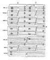
図2は、本発明により与えられる、論理回路クラスターの各行と列とに与えられる、水平と垂直の経路選択用手段と、クロック源と、電位とを示している。
水平の経路選択用手段には、水平経路選択用チャネル(HT)20と、出力経路選択用トラック(OT)22と、第1から第4の水平高速経路選択用チャネル(LDH0−LDH3)24−1から24−4とが、それぞれ含まれる。垂直の経路選択用手段には、垂直経路選択用チャネル(VT)26と、第1から第8垂直高速経路選択用チャネル(LDV0−LDV7)28−1から28−8とが、それぞれ含まれる。
【0021】
水平経路選択用チャネル20と垂直経路選択用チャネル26の各々には、様々な数のトラックを持つ副チャネルが含まれる。水平経路選択用チャネル20は、3トラック,7トラック,9トラック,11トラック,8トラック,4トラックを持つ副チャネルを持っている。水平経路選択用チャネル26は、3トラック,7トラック,9トラック,11トラック,8トラック,8トラック,4トラックを持つ副チャネルを持っている。水平経路選択用チャネル20と垂直経路選択用チャネル26の両方の副チャネル内のトラックは、コアタイル10の長さと幅に渡って配置され、図3Aと図3Bとに描かれる方法で、様々な長さでプログラム可能な要素に分割される。出力経路選択用トラック22は、論理回路クラスター12の幅方向に延びる。4つの水平高速経路選択用チャネル24−1から24−4の各々は、コアタイル10の幅方向で延び、4つのトラックを含む。垂直経路選択用チャネル28−1から28−8の各々は、コアタイル10の全体の長さ方向で延び、4つのトラックを含む。
【0022】
クロック源には、経路選択済みクロックの組(RCLK0とRCLK1とRCLK2とRCLK3)30と、第1から第4の配線済みクロック(HCLK0からHCLK3)32−1から32−4のそれぞれが含まれる。経路選択済みクロックの組30のRCLK0/RCLK1とRCLK2/RCLK3は、論理回路クラスター12の行に交互に結合するが、論理回路クラスター12の行の各々は、それと結合した経路選択済みクロックの組30と、すぐ上の論理回路クラスター12の行と結合する経路選択済みクロックの組30の両方にアクセスする。経路選択済みクロックの組30と配線済みクロック32−1から32−4は、コアタイル10の幅と長さ方向にそれぞれ進む。
【0023】
電位には、コアタイルの幅方向に走る、接地電位(NGND)34とVcc(NVCC)36とが含まれる。
水平経路選択用手段20,22,24と、経路選択用クロック源30と、電位34,36は、I/OクラスターとRAMモジュール14の中に延びて、水平経路選択用手段26と28及び配線済みクロック32のチャネルは、I/Oクラスター16の行の中に延びる。I/Oクラスター16とRAMモジュール14の列の各々は、自身の垂直経路選択用手段26,28と、配線済みクロック32を持ち、I/Oクラスター16の行の各々は、自身の垂直経路選択用手段20,22,24と経路選択済みクロックの組30と電位34,36を持っている。論理回路クラスターの行の再上端部に含まれるのは、水平経路選択用チャネル20と配線済みクロックの組30と電位34,36が含まれるチャネルである。
【0024】
水平経路選択用チャネル20と出力経路選択用トラック22が、垂直経路選択用チャネル26と交差する場所に配置されるのは、白抜きの円で描かれるプログラム可能な要素であり、その内の一つは、参照番号40で示されている。プログラム可能な要素40は、プログラム可能な要素のいくつかの種類の内のいずれかであって良く、その多くは、当業者には良く知られており、アンチヒューズ(antifuse)、パストランジスタ(pass transistor)、SRAMセル、EEPROM要素もしくはセル、フラッシュ要素もしくはセルが含まれる。好ましくは、プログラム可能な要素は、アンチヒューズであることである。アンチヒューズは、当業者には良く知られているが、それゆえ、ここでは、開示が複雑になって本発明が不明瞭になるのを避けるために説明は割愛する。この開示に一貫性を持たせるために、プログラム可能な要素は、参照番号40で示す。
【0025】
図3Aと図3Bは、本発明による、水平及び垂直の経路選択用チャネル20,26の副チャネル内にあるトラックの分割を示している。水平経路選択用チャネル20のセグメント長の単位は、論理回路クラスター12の列の半分であり、水平経路選択用チャネル20内にあるトラックは、論理回路クラスター12のあらゆる列内で自身を繰り返すパターン内で分割される。垂直経路選択用チャネル20のためのセグメント長の単位は、論理回路クラスター12の一つの行であり、論理回路クラスター12の1行置き後に自身を繰り返すパターン内で分割される。プログラム可能な要素40は、水平及び垂直経路選択用チャネル20,26内のトラックを、それぞれ分割するのに使用される。その内の一つが、図3Aと図3Bの両方において参照番号50で示される、ダイレクトアクセス(DA)要素は、アンチヒューズを、好適なプログラム可能な要素40としてプログラムするのに使用されるプログラム素子である。
【0026】
図4には、本発明による、論理回路クラスター12のブロック図である。論理回路クラスター12の各々には、4つの論理回路(LC)モジュール60と、2つのフリップフロップ(FF)モジュール62と、一つのバッファ(B)モジュール64と、4つの送信器(TX)モジュール66と、4つの受信器(RX)モジュール68とが含まれる。
【0027】
図5は、本発明による論理回路モジュール60の図である。論理回路モジュール60は、組み合わせ論理回路ユニットであり、第1と第2と第3と第4のマルチプレクサ62,64,66,68を含み、各々は、第1と第2のデータ入力と、一つの出力と、一つのセレクト入力とを持っている。
【0028】
マルチプレクサ62と64への第1データ入力は、水平経路選択用チャネル20−1あるいは、出力経路選択用トラック22−1あるいは、論理回路モジュール60が配置される論理回路クラスター12の行に結合される電位34−1もしくは36−2へプログラム可能に接続されるだろう。マルチプレクサ62と64への第2データ入力は、水平経路選択用チャネル20−2あるいは、出力経路選択用トラック22−2あるいは、論理回路モジュール60が配置される論理回路クラスター12の行のすぐ上の論理回路クラスター12の行に結合される電位34−2もしくは36−2へプログラム可能に接続されるだろう。マルチプレクサ62と64への第1及び第2データ入力は、別のやり方で、水平経路選択用チャネル20−1あるいは、出力経路選択用トラック22−1あるいは、電位34−1もしくは36−2へ、インバータ70を通してプログラム可能に接続される。
【0029】
マルチプレクサ62,64は、それぞれ、2入力ANDゲート38の出力に結合される共通のセレクト入力を持ち、マルチプレクサ62,64の出力は、マルチプレクサ66の第1と第2データ入力を作る。マルチプレクサ66のセレクト入力は、2入力ORゲート74の出力に接続され、マルチプレクサ66の出力は、マルチプレクサ68の第1データ入力を作る。マルチプレクサ36の第2データ入力は、マルチプレクサ66の出力に接続される第1入力と、高速キャリー入力(FCI)信号に接続される第2入力とを持つ2入力排他的論理和(XOR)ゲート76の出力によって作られる。マルチプレクサ68のセレクト入力は、電位34−2あるいは36−2へ、プログラム可能に接続することができる。マルチプレクサ36の出力HDOUTは、論理回路モジュール20の出力を作る。信号HDOUTは、バッファ78によってバッファされ、出力経路選択用トラック22−1の少なくとも一つに配線される。信号HDOUTは、また、以下に説明するFFモジュール62への入力を作る。
【0030】
ANDゲート72への第1入力は、水平経路選択用チャネル20−1あるいは経路選択済みクロックの組30−1あるいは出力経路選択用トラック22−1あるいは電位34−1もしくは36−1に、プログラム可能に接続することができる。ANDゲート72への第2入力は、水平経路選択用チャネル20−2あるいは経路選択済みクロックの組30−2あるいは出力経路選択用トラック22−2あるいは電位34−2もしくは36−2に、プログラム可能に接続することができる。さもなければ、ANDゲート72への第2入力は、インバータ70を通して、水平経路選択用チャネル20−1あるいは出力経路選択用トラック22−1あるいは電位34−1もしくは36−1に、プログラム可能に接続することができる。
【0031】
ORゲート74への第1入力は、水平経路選択用チャネル20−1あるいは経路選択済みクロックの組30−1あるいは出力経路選択用トラック22−1あるいは電位34−1もしくは36−1に、プログラム可能に接続することができる。ORゲート74への第2入力は、水平経路選択用チャネル20−2あるいは経路選択済みクロックの組30−2あるいは出力経路選択用トラック22−2あるいは電位34−2もしくは36−2に、プログラム可能に接続することができる。さもなければ、ANDゲート74への第2入力は、インバータ70を通して、水平経路選択用チャネル20−1あるいは出力経路選択用トラック22−1あるいは電位34−1もしくは36−1に、プログラム可能に接続することができる。
【0032】
ANDゲート72とORゲート74の出力は、また、FCI信号と共に、第1,第2,第3の2入力ANDゲート80,82,84と3入力ORゲート86とによって実現される専用のキャリー伝搬論理回路に接続される。ANDゲート72の出力は、ANDゲート80,82の第1入力に接続され、ORゲート74の出力は、ANDゲート80の第2入力とANDゲート84の第1入力へ接続され、信号FCIは、ANDゲート82の第2入力とANDゲート84の第2入力に接続される。ANDゲート80,82,84の出力は、ORゲート86の入力を作り、ORゲート86の出力は、高速キャリー出力(FCO)信号を作る。論理回路モジュール60において、FCI信号は、同じ列内のすぐ隣りと上の論理回路モジュール60のFCO信号出力である。FCI信号とFCO信号とは、リップルタイプの算術関数の率を増加させるのに使用される。
【0033】
図6は、本発明によるFFモジュール62の図である。FFモジュール62は、順序回路ユニットであり、4入力マルチプレクサ90を含み、これは、第1及び第2セレクト入力と、一つのセレクト入力を持つ第1及び第2及び第3の2入力マルチプレクサ92,94,96と、Dフリップフロップ96を持っている。
【0034】
4入力マルチプレクサ90の4つの入力は、32−1から32−4の4本の配線済みクロック信号に接続され、第1及び第2のセレクト入力は、FFモジュール62が配置される論理回路クラスター12の行に結合される電位34−1あるいは36−1にプログラム可能に接続される。
【0035】
第1の2入力マルチプレクサ64は、水平経路選択用チャネル20−2、あるいは出力経路選択用トラック22−2、あるいはFFモジュール62が配置される論理回路クラスター12の行のすぐ上の論理回路クラスター12の行と結合する電位34−2もしくは36−2とプログラム可能に接続することのできる第1データ入力と、信号HDOUTに接続する第2データ入力と、水平経路選択用チャネル20−2、あるいは出力経路選択用トラック22−2、あるいは電位34−2もしくは36−2とプログラム可能に接続することのできるセレクト信号とを持っている。
【0036】
第2の2入力マルチプレクサ94は、4入力マルチプレクサ90の出力に接続される第1データ入力と、水平経路選択用チャネル20−1、あるいは経路選択用クロックの組30−1、あるいは出力経路選択用トラック22−1、あるいは電位36−1とに対して、または、水平経路選択用チャネル20−2、あるいは経路選択用クロックの組30−2、あるいは出力経路選択用トラック22−2、あるいは電位36−2に対して、バッファ100を通してプログラム可能に接続することのできる第2データ入力とを持っている。第2の2入力マルチプレクサ94は、電位34−1あるいは36−1にプログラム可能に接続することのできるセレクト入力を持っている。
【0037】
第3の2入力マルチプレクサ96は、第1の2入力マルチプレクサ92の出力に接続される第1データ入力と、Dフリップフロップ70の出力に接続される第2データ入力と、水平経路選択用チャネル20−1、あるいは経路選択用クロックの組30−1と、あるいは出力経路選択用トラック22−1と、あるいは電位34−1もしくは36−1とプログラム可能に接続することのできるセレクト入力を持っている。
【0038】
Dフリップフロップ70は、第3の2入力マルチプレクサ68の出力に接続されるデータ入力と、第2の2入力マルチプレクサ66の出力に接続される第1入力と電位34−2もしくは36−2にプログラム可能に接続することのできる第2入力とを持つ2入力排他的論理和ゲート102の出力に接続されるクロック入力と、水平経路選択用チャネル20−1あるいは経路選択用クロックの組30−1あるいは出力経路選択用トラック22−1あるいは電位34−1もしくは36−1にプログラム可能に接続することのできるクリア入力およびプリセット入力と、出力経路選択用トラック22−1の少なくとも一つに配線されるバッファによってバッファされる出力とを持っている。
【0039】
図7は、本発明による、バッファモジュール64の図である。バッファモジュール64には、水平経路選択用チャネル20−1あるいは出力経路選択用トラック22−1あるいはこのバッファモジュール64が配置される論理回路クラスター12の行に結合される電位36−1に対して、または、水平経路選択用チャネル20−1あるいは出力経路選択用トラック22−2あるいはバッファモジュール64が配置される論理回路クラスター12の行のすぐ上の論理回路クラスター12の行に結合される電位36−2に対してプログラム可能に接続することのできる入力をもったバッファ120が含まれている。バッファ120の出力は、出力経路選択用トラック22−1の少なくとも一つに配線される。
【0040】
図8は、本発明による送信器モジュール66の図である。送信器モジュール66には、水平経路選択用チャネル20−1あるいは出力経路選択用トラック22−1あるいは電位36−1あるいは送信器モジュール66が配置される論理回路クラスター12の行に結合されるVCC電位のLDNVCC132に対して、または、水平経路選択用チャネル20−2あるいは出力経路選択用トラック22−2あるいは送信器モジュール66が配置される論理回路クラスター12の行のすぐ上の論理回路クラスター12の行に結合される電位36−2に対してプログラム可能に接続することのできる入力をもったバッファ130が含まれる。バッファ130の出力は、水平高速経路選択用トラック24−1−1に、あるいは垂直高速経路選択用トラック28−1にプログラム可能に接続することができる。加えて、バッファ130は、水平高速経路選択用トラック24−1−1から垂直高速経路選択用トラック28−1へ、あるいは、垂直高速経路選択用トラック28−1から水平経路選択用トラック24−1−1へ、信号を転送するためにプログラム可能に接続することができる。バッファ130は、信号強度を上げるのに使用することができることを理解されたい。
【0041】
図9は、本発明による、論理回路クラスター12の隣接する行と列にそれぞれ結合される、水平及び垂直経路選択用トラック24,28の間における、送信器モジュール66の配置パターンを示す図である。図に描かれる様に、交点からの、水平及び垂直の高速経路選択用トラック24,28である。これらの交点における、送信器モジュール66の配置において、各水平高速経路選択用チャネル24は、垂直高速チャネル28−1と水平経路選択用チャネル28−2の一つとの交点に置かれる送信器モジュール66を持ち、各垂直高速経路選択用チャネル28は、水平高速チャネル24−1と水平高速経路選択用チャネル24−2の交点に置かれる送信器モジュール66を持っている。
【0042】
図10は、本発明による受信器モジュール68を示す図である。受信モジュール28には、第1もしくは第2の水平高速経路選択用チャネル24−4−1,24−1−2、あるいは第1もしくは第2の垂直高速経路選択用チャネル28−1,28−2、あるいは受信器モジュール68が配置される論理回路クラスター12の行あるいは列に結合される電位132にプログラム可能に接続することができる入力を持つバッファ140が含まれる。バッファ140の出力は、経路選択用トラック22−1の少なくとも一つに配線される。
【0043】
図11は、本発明による、論理回路クラスター12の隣接する行と列にそれぞれ結合される水平および垂直の高速経路選択用トラック24と28の間における、送信器モジュール66の配置パターンを示す図である。図に描かれる様に、交点からの、水平及び垂直の高速経路選択用トラック24,28である。これらの交点における受信器モジュール68の配置において、各水平高速経路選択用チャネル24は、2つの受信器モジュール68に結合され、各垂直高速経路選択用チャネル68は、一つの受信器モジュール68に結合される。
【0044】
図12は、本発明によるRAMブロック14を示した図である。RAMブロック14において、メモリ要素は、ブロック150として描かれる。ブロック150におけるメモリ要素について、ここでは、開示が複雑になって本発明が不明瞭になるのを避けるために説明は割愛する。RAMブロック14は、読み出しと書き込みの動作を同時に行うために、デュアルポートである。SRAMブロック150のビット構成は、128個の36ビット幅のワードか、256個の18ビット幅のワードか、512個の9ビット幅のワードか、1K個の4ビット幅のワードか、4K個の1ビット幅のワードとして作ることができる。全てのワード幅が、下位ビットが下位アドレスにあるように、記憶され読み出される。
【0045】
SRAMブロック150への入力には、書き込みアドレス(S_WA)と、読み出しアドレス(S_RA)と、書き込みデータ(S_WD)と、書き込みイネーブル(S_WE)と、書き込みクロック(S_WC)と、読み出しイネーブル(S_RE)と、ブロックイネーブル(BLK_EN)と、衝突検出イネーブル(COL_DET)とが含まれる。SRAMブロック150からの出力には、読み出しデータ(S_RD)と衝突検出(S_COLL)とが含まれる。
【0046】
データをRAMブロック14に書き込むには、1ビットの書き込みクロック(WCK)データバスと、5ビットの書き込みイネーブル(WEN)データバスと、12ビットの書き込みアドレスバス(WAD)と、第1から第4の9ビットの書き込みデータバス(WDA,WDB,WDC,WDD)が与えられる。RAMブロック14にデータを読み出すには、1ビットの読み出しクロック(RCK)データバスと、5ビットの読み出しイネーブル(REN)データバスと、12ビットの読み出しアドレスバス(RAD)と、第1から第4の9ビットの書き込みデータバス(RDA,RDB,RDC,RDD)が与えられる。書き込みデータは、4つのWD(AからD)バスの各々によってRAMブロック14に転送し、RAMブロック14からの読み出しデータは、4つのRD(AからD)バスの各々に転送することができる。
【0047】
WCKバスはSRAMブロック150のS_WC入力に接続される。WCKバス上の信号の極性は、プログラム可能なインバータ152によって選択されるか、プログラム可能に接地電位に接続することができる。WENバスからの5つの信号は、その出力がSRAMブロック150のS_WE入力に接続されるANDゲート154に接続される。WENバス上の信号の各々の極性は、その内の一つは参照番号152によって示されるか、プログラム可能にハイに吊られるかする、プログラム可能なインバータによって選択されることができる。WAバス上の12個の信号は、SRAM150のS_WA入力に接続される。これらの信号の各々は、接地電位にプログラム可能に接続することができる。
【0048】
4つのWD(AからD)バスの各々の上の9個の信号は、SRAMブロック150のS_WA入力に接続される。これらの信号の各々は、プログラム可能に接地電位に接続することができる。4つのWD(AからD)バスの各々からの8個の低位の信号もまた、パリティ生成器を形成する論理和(XOR)ゲート156の入力に接続される。XORゲート156の出力は、4つのWD(AからD)バスの各々からの高位の信号を形成するのにプログラム可能に接続することができる。
【0049】
WD(AからD)バスからの9個の信号もまた、16:8の衝突検出器マルチプレクサ158の入力に接続される。S_RD出力からの9個の出力信号もまた、18:9の衝突検出器マルチプレクサ158の入力に接続される。S_COLL出力信号は、衝突検出器マルチプレクサ174へのセレクト入力を形成して、9個のWD信号或いは9個のRD信号のいずれかを選択する。18:9衝突検出器マルチプレクサ158の出力は、以下に説明するように、通過させるかラッチするように構成することのできるフリップフロップ160の入力に結合される。フリップフロップ160の出力は、読み出しデータRD(AからD)バスに結合される。18:9マルチプレクサ158からの9個の出力信号もまた、パリティチェックを作る排他的論理和(XOR)ゲート162の入力に接続される。XORゲート162の出力は、18:9マルチプレクサ158から出力される高位の信号にプログラム可能に接続することができる。
【0050】
RCKバスは、以下に説明するように通過させるかラッチするように構成することができるフリップフロップ164のクロック入力に接続され、またフリップフロップ160に接続される。RCKバス上の信号の極性は、プログラム可能なインバータ152によって選択可能である。RENバスからの5個の信号は、その出力がフリップフロップ164の第1データ入力に接続されるANDゲート166に接続される。RENバス上の5個の信号の各々の極性は、プログラム可能なインバータによって選択することができ、その内の一つは、参照番号152で示されるか、プログラム可能にハイに吊られる。WAバス上の12個の信号は、フリップフロップ164の第2から第19のデータ入力に接続される。これらの信号の各々は、プログラム可能に接地電位に接続することができる。フリップフロップ164の第1データ入力に対応するフリップフロップ164の第1出力は、SRAM150のS_RE入力に、またフリップフロップ160のイネーブル入力に接続される。フリップフロップ164の第2から第19データ入力に対応するフリップフロップ164の第2から第19データ出力は、SRAM150のS_RA入力に接続される。
【0051】
フリップフロップ160と164は、信号TLFF1とTLFF1によって独立に構成することができ、それぞれデータを通過させるかラッチする。フリップフロップ164は、RAとRENを同期させ、一方、160は、SRAM150から読み出したデータを同期させる。フリップフロップ160と164の組合せは、4つの異なるモードで使用することができる。
【0052】
フリップフロップ160と164は、共に通過させ、読み出し動作は、非同期である。このモードは、RCK信号を必要とせず、RCK信号は、強制的にオフにされる。RAからのデータは、全てのRENがハイの時にRDに現れる。
【0053】
フリップフロップ160がラッチされ、フリップフロップ164が通過させる時、読み出し動作は、同期式の1段のパイプラインである。RCKの活性弧において、全てのRENがハイのとき、RAからのデータは、RDに現れる。実際のメモリアクセス時間は、RAとRENのセットアップ時間に含まれ、データの読み出し時間は、RCKに関して最小である。
【0054】
フリップフロップ160が通過させ、フリップフロップ164がラッチする時、読み出し動作は、同期式の1段のパイプラインである。RCKの活性弧において、全てのRENがハイのとき、RAからのデータは、RDに現れる。RAとRENのセットアップ時間は、RCKに関して最小である。実際のメモリアクセス時間は、読み出し時間に含まれる。
【0055】
フリップフロップ160と164が、共に、ラッチされる時、読み出し動作は、同期式の2段のパイプラインである。2つのアクティブRCKサイクルが、データをRAからRDに伝搬させるのに必要である。第1のRCKサイクルで、RAとRENをセットアップし、第2のRCKサイクルで、メモリにアクセスして読み出しRDをセットアップする。
【0056】
図13は、本発明によるI/Oクラスター16のブロック図である。I/Oクラスター16には、第1および第2のI/Oモジュール200と、バッファモジュール202と、第1から第4の送信器モジュール204と、第1から第4受信器モジュール204が含まれる。バッファと送信器と受信器のモジュール202,204,206は、それぞれ、図1,8,10で描かれたものに似ているので、ここでは、開示が複雑になって本発明が不明瞭になるのを避けるために説明は割愛する。
【0057】
図14は、本発明による、I/Oモジュール200の詳細なブロック図である。I/Oモジュールには、FIFO210と、入力フリップフロップ(INFF)212と、出力フリップフロップ214と、イネーブルフリップフロップ(ENFF)216とが含まれる。I/O選択モジュール220による異なった動作モードのいずれかに置かれ、各I/Oモジュール200に関連するI/Oパッド218は、入力バッファ222と出力バッファ224に結合される。境界スキャンレジスタ(BSR)モジュール226は、入力バッファ222と出力バッファ224に、またFIFO210に結合される。BSR226とFIFO210を実現するのは、当業者の技術水準で可能であり、ここでは、開示が複雑になって本発明が不明瞭になるのを避けるために説明は割愛する。FIFOは、入力データ、あるいは出力データ、あるいは出力イネーブルをバッファすることも、通過することもできる。
【0058】
I/O選択モジュール220の入力は、出力バッファ222に対して、ホット挿入(hot insertion)と3.3Vの許容量、およびプログラム可能なスルーレート、および微弱なプルアップもしくはプルダウン回路、および4つの異なる駆動力(drive strenfth)を提供し、また入力バッファ224に対して、I/O内に登録される入力信号のためにゼロ保持時間を補償する入力遅延を提供するのに置かれるために、その中にI/Oモジュール200が置かれるI/Oクラスター16の行に関連する電位34−1或いは34−2にプログラム可能に接続することができる。
【0059】
FIFOモジュール210には、入力DIR0とDIR1とIENBとICRBとOENBとOCRBとEENBとECLRBとICKとOCLKとECLKが含まれる。加えて、FIFOモジュール210は、BSRモジュール226とOUTFF214およびENFF216と、BSRモジュール226に接続される第1および第2データ出力と、INFF212のHDIN入力に接続されるデータ出力とを持つ。
【0060】
FIFO210は、入力DIR0とDIR1に制御される4つのモジュールを持つ。第1モードでは、FIFO210は、オフになり、全ての信号を通過させる。第2モードでは、FIFO210は、出力イネーブルをバッファし、入力データと出力データとを通過させる。第3モードでは、FIFO210は、出力データをバッファし、入力データと出力データとを通過させる。第4モードでは、FIFO210は、入力データをバッファし、出力データと出力イネーブルを通過させる。入力DIR0とDIR1の各々は、水平経路選択用チャネル20−1、あるいは電位34−1もしくは36−1にプログラム可能に接続される。FIFOモジュール210への残りの入力は、入力と出力のINFF212とOUTFFR214とENFF216に従って説明される。
【0061】
INFF212は、入力CKS1とCKS2とRCLKAとSOとCLRBとPSETBとRCLKBとS1とCKSOとCKPとHDINとHCLK、および出力YとCOUTを持っている。入力CKS1とCKS2の各々は、電位34−1あるいは36−1に、プログラム可能に接続することができる。RCLKAは、水平経路選択用チャネル20−1、あるいは経路選択用クロックの組30−1、あるいは電位36−1、あるいは出力経路選択用トラック22−1にプログラム可能に接続することができる。入力S0,CLRB,PSETBの各々は、水平経路選択用チャネル20−1、あるいは経路選択用クロックの組30−1、あるいは電位34−1もしくは36−1、あるいは出力経路選択用トラック22−1にプログラム可能に接続することができる。入力CKS0とCKPの各々は、その中にINFF212が置かれるI/Oクラスター16のすぐ上のI/Oクラスター16に関連する電位34−2あるいは36−2にプログラム可能に接続することができる。RCLKBは、水平経路選択用チャネル20−2、あるいは経路選択用クロックの組30−2、あるいは電位36−2、あるいは出力経路選択用トラック22−2にプログラム可能に接続することができる。S1は、水平経路選択用チャネル20−2、あるいは電位34−2もしくは36−2、あるいは出力経路選択用トラック22−2にプログラム可能に接続することができる。入力HCLKは、HCLK0とHCLK1とHCLK2とHCLK3のそれぞれ32−1から32−4に接続される。出力Yは、出力経路選択用トラック22−1に配線される。
【0062】
OUTFF214は、CKS1とCKS2とRCLKAとSOとCLRBとPSETBとRCLKBとDINとS1とCKSOとCKPとHCLK、および出力YとCOUTとYOUTを持っている。入力CKS1とCKS2の各々は、電位34−1あるいは36−1に、プログラム可能に接続することができる。RCLKAは、水平経路選択用チャネル20−1、あるいは経路選択用クロックの組30−1、あるいは電位36−1、あるいは出力経路選択用トラック22−1にプログラム可能に接続することができる。入力S0,CLRB,PSETBの各々は、水平経路選択用チャネル20−1、あるいは経路選択用クロックの組30−1、あるいは電位34−1もしくは36−1、あるいは出力経路選択用トラック22−1にプログラム可能に接続することができる。入力CKS0とCKPの各々は、電位34−2あるいは36−2にプログラム可能に接続することができる。RCLKBは、水平経路選択用チャネル20−2、あるいは経路選択用クロックの組30−2、あるいは電位36−2、あるいは出力経路選択用トラック22−2にプログラム可能に接続することができる。入力DINとS1の各々は、水平経路選択用チャネル20−2、あるいは電位34−2もしくは36−2、あるいは出力経路選択用トラック22−2にプログラム可能に接続することができる。入力HCLKは、HCLK0とHCLK1とHCLK2とHCLK3のそれぞれ32−1から32−4に接続される。出力Yは、出力経路選択用トラック22−1に配線される。
【0063】
ENFF216は、CKS1とCKS2とRCLKAとSOとCLRBとPSETBとRCLKBとDINとS1とCKSOとCKPとHCLK、および出力YとCOUTとYOUTを持っている。入力CKS1とCKS2の各々は、電位34−1あるいは36−1に、プログラム可能に接続することができる。RCLKAは、水平経路選択用チャネル20−1、あるいは経路選択用クロックの組30−1、あるいは電位36−1、あるいは出力経路選択用トラック22−1にプログラム可能に接続することができる。入力S0,CLRB,PSETBの各々は、水平経路選択用チャネル20−1、あるいは経路選択用クロックの組30−1、あるいは電位34−1もしくは36−1、あるいは出力経路選択用トラック22−1にプログラム可能に接続することができる。入力CKS0とCKPの各々は、電位34−2あるいは36−2にプログラム可能に接続することができる。RCLKBは、水平経路選択用チャネル20−2、あるいは経路選択用クロックの組30−2、あるいは電位36−2、あるいは出力経路選択用トラック22−2にプログラム可能に接続することができる。入力DINとS1の各々は、水平経路選択用チャネル20−2、あるいは電位34−2もしくは36−2、あるいは出力経路選択用トラック22−2にプログラム可能に接続することができる。入力HCLKは、HCLK0とHCLK1とHCLK2とHCLK3のそれぞれ32−1から32−4に接続される。出力Yは、出力経路選択用トラック22−1に配線される。
【0064】
INFF212とOUTFF214とENFF216の、SOおよびCLRB入力もまた、FIFO210のそれぞれIENBおよびICLRBと、OENBおよびOCLRBと、EENBおよびECLRBに接続される。INFF212とOUTFF214とENFF216の出力COUTは、FIFO210のICLKとOCLKとECLK入力にそれぞれ接続される。OUTFF214とENFF216のYOUT出力は、FIFO210へのデータ入力として接続される。
【0065】
図15Aは、本発明によるINFF212の、より詳細な図である。INFF212において、4入力マルチプレクサ240は、4つの入力HCLK0,HCLK1,HCLK2,HCLK3と、2つの選択入力CKS1とCKS2を持っている。4入力マルチプレクサ240が選択したクロック入力は、2入力マルチプレクサ242の第1入力に接続される出力を作る。2入力マルチプレクサ242第2入力は、クロック信号RCLKAあるいはRCLKBのいずれかをバッファするバッファ244の出力に接続される。2入力マルチプレクサ242は、CKSO信号に接続されるセレクト入力を持っている。2入力バッファ242の出力は、排他的論理和(XOR)ゲート246の第1入力に接続される。XORゲート246の第2入力は、クロック信号CKPに接続される。XORゲート246の出力は、Dフリップフロップ248のクロック入力に接続される。さらに、4入力マルチプレクサ240とバッファ244と2入力マルチプレクサ242とXORゲート246とに選択されるクロック信号は、クロック出力COUTを作る。Dフリップフロップ248のデータ入力は、データ信号HDINに接続される第1入力と、Dフリップフロップ248のデータ出力に接続される第2入力とを持つ2入力マルチプレクサ250の出力に接続される。2入力マルチプレクサ250は、セレクト信号SOを持っている。データ入力信号HDINもまた、第2入力に接続されるDフリップフロップ248の出力とともに、2入力マルチプレクサ252の第1入力に接続される。2入力マルチプレクサ252は、セレクト入力S1を持ち、2入力マルチプレクサ252の出力は、出力Yを作るためにバッファ254によってバッファされる。
【0066】
図15Bは、本発明による、出力フリップフロップ214とイネーブルフリップフロップ216を、より詳細に示した図である。図15Bは、図14および図15Aと、3つの点で異なるだけであることを理解されたい。第1に、2入力マルチプレクサ250と252への、データ信号DINが、データ信号HDINに置き換わる。第2に、Dフリップフロップ248の出力が、2入力マルチプレクサ252の出力でなく、直接にバッファされたY出力を作っている。第3に、2入力マルチプレクサ252の出力が、出力YOUTを作っている。
【0067】
図16は、本発明による、使用に適した、直並列変換器(deserializer)/並直列変換器(serializer)(LVDS)コア260を示した図である。LVDSコア260は、I/Oパッド218とFIFO210の間で、入力信号と出力信号とを使用することができる。LVDSコア260には、データを受け取るための回路262と、データを送るための回路264とが含まれる。LVDSコア260は、6個のMODE[0:5]ビット上で動作する。MODE[0:5]の最初の2ビットは、LVDSのI/Oの周波数の動作範囲を決定する。LVDSコア260では、2.5Gbpsで1つの送信と1つの受信とのチャネルの外部帯域幅が使用でき、1.25Gbpsで2つの送信と2つの受信とのチャネルの外部帯域幅が使用でき、622Mbpsで4つの送信と4つの受信とのチャネルの外部帯域幅が使用できる。MODE[0:5]の2番目の2ビットで、LVDSのI/Oの並列化と直列化の比率が決定する。受け取ったチャネルは、1:4および1:8および1:16の比率並列化することができる。送ったチャネルは、4:1および8:1および16:1の比率で直列化することができる。MODE[0:5]の3番目の2ビットで、リンクレイヤーの選択肢である、通過あるいは4B/5Bあるいは8B/10Bあるいは高速I/Oを選択する。
【0068】
受信器回路262には、入力バッファ266と、直並列変換器268と、クロック復旧回路270と、データ復号器272と、位相調整器274とが含まれる。各入力バッファ262は、4つのI/Oパッドを含むLVDS I/Oに接続され、その内の二つは、差動対(differential pair)用であり、その内の二つは、Vccと接地電位用である。各入力バッファ266は、MODE[0:5]に制御される直並列変換器268の入力に接続される出力を持っている。各直並列変換器268の出力は、クロック復旧回路270とデータ復号器272の入力に接続される。各クロック復旧回路270は、78Mhzで運転する入力として、基準クロックを持ち、直並列変換器268とデータ復号器272の組に接続される出力と、位相調整器274を持っている。位相調整器274の出力は、FIFOに接続される。各クロック復旧回路270は、またANDゲート276に接続される出力を持ち、これは、LOCK信号を与えるANDチェーンの一部を形成する。クロック復旧回路270によって、組み込みクロックは、受け取ったチャネルから復旧される。
【0069】
送信器回路264には、出力バッファ280と、並直列変換回路(serializer circuit)282と、クロック合成回路284と、データ符号化器286とが含まれる。各出力バッファ280は、4つのパッドLVDS I/Oに接続され、並直列変換回路282の出力に接続される入力を持っている。各並直列変換回路282は、データ符号化器286の出力に接続される入力を持っている。並直列変換回路282とデータ符号化器286は、共に、MODE[0:5]に制御され、また155Mhzで運転するSYS_CLKを入力として持つクロック合成回路284の出力に接続される。データ符号化器は、FIFOの出力に接続される入力を持つ。
【0070】
図17は、本発明による、システム・オン・ア・チップ(SOC)のアーキテクチャ300を示した図であり、この中には、FPGAコアタイル10および関連する仮想部品インターフェイス(VCI)論理回路302と、マイクロコントローラ304および関連するVCI論理回路306と、外部インターフェイス回路JTAG308およびUART312およびそれぞれに関連するVCI論理回路310と314と、システム/周辺バスとブリッジ304および関連するVCI論理回路(図示せず)が含まれる。FPGAコアタイル10に関連するI/O構造は、含まれないことに注意したい。SOC300の内部の接続をより細かく説明するのに、FPGAコアタイル10の経路選択用資源が、バス318によって接続される図の端部に描かれる。これらの経路選択用資源は、FPGAコアタイル10の内部にあることを理解されたい。外部インターフェイス回路JTAG308とUART312と関連するVCI論理回路310と314は、専用のI/Oモジュール320と322によって、外部のSOC300と通信する。
【0071】
部品10,304,308,312,316の各々に関連するVCI論理回路302,306,310,314は、関連する部品の各々の信号を、SOC300内の残りの部品によって理解される標準プロトコルを作る共通の信号に変換するように設計される。第1の部品から第2の部品への信号のやり取りには、第1の部品からの信号のいくらかが、第1の部品に関連するVCIによって共通の信号に最初に変換される必要がある。これらの共通の信号は、第2の部品と関連するVCIによって、第2の部品が正常に動作する信号へと変換される。第1の部品からの信号の他のものは、直接に第2の部品に接続される。システム/周辺バス316が、第1の部品から第2の部品へ変換された信号をバス324を用いてやり取りするのに使用される時、このやり取りは、また共通の信号をシステム/周辺バス316の上へ、あるいはそこへ乗せずに変換する必要があるだろう。本発明により、使用に適したシステム/周辺バス316は、www.arm.comでARMによる、Advanced Microcontroller Bus Architecture(AMBA)として提案されている。
【0072】
第1の部品と第2の部品との間の典型的な通信において、起動装置として知られる第1部品と、対象として知られる第2の部品は、簡単なハンドシェーク(hand−shake)を実行し、起動装置は、対象によって応答される一つあるいは二つ以上の要求を発する。要求は、典型的には、アドレスと、書き込みデータと、いくらかのフラグとから成る。応答は、起動装置により作られた要求と同じ順番で、対象によって、起動装置による要求に対して行われる。VCIパラメータとハンドシェークと要求および応答を始める、本発明による使用に適した仮想部品インターフェイス標準は、http:/www.vsi.orgのVSI Alliance(登録商標)によって提案されている。
【0073】
仮想部品インターフェイス標準によると、起動装置からの要求を対象に回し、そして対象からの応答を起動装置へ回す前に、起動装置と対象との同期を取るために、ハンドシェークが、起動装置と対象との間で最初に実行される。一旦、ハンドシェークが起こると、要求と応答は、セルとして起動装置と対象の間で転送される。これらのセルは、パケットにまとめられて、パケットはパケットチェーンにまとめられるだろう。
【0074】
要求の内容は、3つの信号グループに分割される。第1のグループは、操作コード(op−code)を備えて、作られた要求の種類を特定する。第2のグループには、パケット長とチェーン化のための制御信号が含まれる。第3のグループには、アドレスとデータの情報が含まれる。操作コードのグループには、操作が無いか、読み込み操作か、書き込み操作か、読み込み固定操作かどうかを示す命令領域が含まれる。操作コード領域は、またアドレス情報のためのフラグを含む。パケット長とチェーンのグループには、パケット長とパケットのチェーン長とチェーン固定情報が含まれる。アドレスとデータのグループには、アドレス情報と、書き込みデータと、バイトイネーブル情報とが含まれる。応答の内容には、応答を扱うことができるかどうかを示す応答誤り領域と、読み出し要求とパケット信号の終了の結果として戻ってきた読み出しデータが含まれる。
【0075】
本発明による特定の実施形態において、Mentor Graphics, Wilsonville, ORからのマイクロコントローラM8051によって実現されるマイクロコントローラ302は、SOC300内のFPGAコア10にインターフェイスする。マイクロコントローラ302には、8051MC330と、ランダムアクセスメモリ(RAM)モジュール332と、読み出し専用メモリ(ROM)モジュール334と、レジスターファイル336と、入出力FIFOのそれぞれ338および340が含まれる。8051MC330と、RAM332と、ROM334と、レジスターファイル336は、VCI306とやり取りする内部CPUバス342と結合される。バス344は、FPGA経路選択用チャネルに直接接続するマイクロコントローラ302によって使用される。
【0076】
8051マイクロコントローラには、3つの種類の信号がある、すなわち、プロセッサ入力と、プロセッサ出力と、共通VCI信号あるいは直接信号に変換することのできる機能的内部接続信号である。
FPGAコアタイル10の経路選択用チャネルに直接接続されるプロセッサ入力には、非外部アクセス信号(NEA)と、発振器からのクロック入力(NX1)と、遊休時に停止可能な発振器からのクロック入力(NX2)と、リセット状態フラグ信号(RST)と、第1および第2ダウンロードモードセレクト(ALEIとPSEI)が含まれる。VCI306によってやり取りされるプロセッサ入力と、システム/周辺バス316と、VCI302と、FPGAコアタイル10の経路選択用チャネルには、共通信号WDATAに変換される4つの8ビット入力ポート(A[7:0],B[7:0],C[7:0],D[7:0])が含まれる。
【0077】
FPGAコアタイル10の経路選択用チャネルに直接接続されるプロセッサ入力には、ポートデータポート(AE[7:0],BE[7:0],CE[7:0],DE[7:0])のための8ビット双方向制御線を4組と、アドレスラッチイネーブル(ALE)と、外部プログラムメモリイネーブル(NPSEN)と、ALEとPSENのための双方向制御線(NALEN)と、発振器ディスエーブル制御信号(XOFF)と、遊休モードクロック修飾子(IDLE)が含まれる。VCI306によってやり取りされるプロセッサ入力と、システム/周辺バス316と、VCI302と、FPGAコアタイル10の経路選択用チャネルには、共通信号RDATAに変換される4つの8ビット入力ポート(OA[7:0],OB[7:0],OC[7:0],OD[7:0])が含まれる。
【0078】
機能的内部接続信号には、入力信号と出力信号とが含まれる。FPGAコアタイル10の経路選択用チャネルに直接接続される機能的内部接続入力信号には、非外部特別機能レジスター肯定応答(NESFR)が含まれる。VCI306によってやり取りされるプロセッサ入力と、システム/周辺バス316と、VCI302と、FPGAコアタイル10の経路選択用チャネルには、8ビットプログラムメモリデータバス(MD[7:0])と、共通信号WDATAに変換されるレジスターファイルデータ入力(FI[7:0])が含まれる。FPGAコアタイル10の経路選択用チャネルに直接接続される機能的内部接続入力信号には、プログラムメモリ出力イネーブル(NMOE)と、プログラムメモリ書き込みストローブ(NWME)と、プログラムメモリダウンロードモード(DLM)と、レジスターファイル出力イネーブル(NFOE)と、レジスターファイル書き込みストローブ(NFWE)と、外部特別機能出力イネーブル(NSFROE)と、外部特別機能書き込みストローブ(NSFRWE)が含まれる。VCI306によってやり取りされる機能的内部接続出力信号と、システム/周辺バス316と、VCI302と、FPGAコアタイル10の経路選択用チャネルには、共通信号RDATAに変換されるレジスターファイルデータ出力(FO[7:0])と、共通信号ADDRESSに変換されるレジスターファイルアドレスラインとプログラムメモリアドレスライン(FA[7:0]とM[15:0])が含まれる。
【0079】
本発明の実施形態と用途を示し説明したが、上述したよりも更に多くの変更が、ここの本発明の要旨から逸脱せずに可能であることは当業者には明らかであろう。従って、本発明は、添付した特許請求の範囲によってのみ制限される。
【図面の簡単な説明】
【図1】本発明によるFPGAコアタイルのブロック図である。
【図2】本発明によって、FPGAコアタイル内の論理回路クラスターの各行と列とに与えられる、経路選択用手段と、クロック源と、電位とを示す図である。
【図3A】本発明による、FPGAコアタイル内の水平の経路選択用チャネルの副チャネル内におけるトラックの分割を示す図である。
【図3B】本発明による、FPGAコアタイル内の垂直の経路選択用チャネルの副チャネル内におけるトラックの分割を示す図である。
【図4】本発明による、論理回路クラスターのブロック図である。
【図5】本発明による、論理回路モジュールの図である。
【図6】本発明による、フリップフロップモジュールの図である。
【図7】本発明による、バッファモジュールの図である。
【図8】本発明による、変換モジュールの図である。
【図9】本発明による、水平と垂直の高速経路選択用トラックの間の、送信モジュールの配置パターンの図である。
【図10】本発明による、受信器モジュールの図である。
【図11】本発明による、本発明による、水平と垂直の高速経路選択用トラックの間の、送信モジュールの配置パターンの図である。
【図12】本発明による、ランダムアクセスメモリブロックの図である。
【図13】本発明による、I/Oクラスターのブロック図である。
【図14】本発明による、I/Oモジュールのブロック図である。
【図15A】本発明による、入力フリップフロップモジュールの図である。
【図15B】本発明による、出力フリップフロップモジュールの図である。
【図16】本発明による使用に適した、直並列変換器/並直列変換器(LVDS)コアの図である。
【図17】本発明による、システム・オン・ア・チップのアーキテクチャの図である。
【符号の説明】
10…コアタイル
12…論理回路クラスター
14…RAMモジュール
16…I/Oクラスター
40…プログラム可能な要素
60…論理回路(LC)モジュール
62…フリップフロップ(FF)モジュール
64…バッファ(B)モジュール
66,204…送信器(TX)モジュール
68,206…受信器(RX)モジュール
150…SRAMブロック
200…I/Oモジュール
212…入力フリップフロップ
214…出力フリップフロップ
216…イネーブルフリップフロップ[0001]
TECHNICAL FIELD OF THE INVENTION
The present invention relates to a system-on-a-chip architecture. More specifically, the present invention relates to field programmable gate arrays and microcontrollers in a system-on-a-chip architecture.
[0002]
2. Description of the Related Art
Integrated circuits use a network of metal interconnects between individual semiconductor components that are patterned by standard photolithographic processes during wafer fabrication. Numerous metal patterns may be used to increase the interconnect flexibility.
[0003]
It has been believed that user-programmable interconnect technology reduces tool costs and speeds delivery times. Finally, a field programmable gate array (FPGA) was developed. An FPGA is an array of undefined gates with undefined wiring channels. To implement the function of a particular circuit, the circuit is mapped into an array and the wiring channels and appropriate connections are programmed to implement the wiring connections that make up the function of the circuit.
[0004]
A gate array can perform virtually any combination of functions. The input signal is processed by a programmed circuit to produce the desired combination of outputs. Such input from the user system flows through the input buffer, through the circuit, and finally through the output buffer and back to the user system. Such buffers provide any or all of the following input / output (I / O) functions, voltage gain, current gain, level translation, delay, signal isolation, and hysteresis.
[0005]
Inevitably, there are two configurations of programmable circuit elements for using the various FPGAs that are user programmable. As an example of a first configuration, the example disclosed in US Patent No. 4,758,745 to EL Gamal et al. Is permanently programmable by a user. As a second configuration example, the example disclosed in Freeman's U.S. Pat. No. 4,870,302 is variably programmable by a user.
[0006]
Application specific integrated circuits (ASICs), such as microcontrollers, are mask-programmable gate arrays that offer higher functionality and higher performance and space than FPGAs, which offer lower cost designs and higher user adaptability. Provide more efficient use. Also, ASICs can perform various I / O functions often faster than FPGAs. Other dedicated functional circuits can also provide higher functionality and performance than the equivalent composed of FPGA components.
[0007]
In a system-on-a-chip with both an FPGA and an ASIC, some of the advantages of both designs are provided. The primary consideration when designing an SOC is to provide an appropriate interface between the FPGA and a portion of the ASIC. In order for the IC to perform its tasks correctly, the FPGA and part of the ASIC must be able to effectively communicate with each other.
[0008]
[Means for Solving the Problems]
In the present invention, an FPGA core tile is used as a stand-alone FPGA, where the same is arranged in a rectangular array of core tiles and included with other elements in a system-on-a-chip (SOC). It is possible to be. The core tile includes a cluster of logic circuits, a module of random access memory (RAM), and a cluster of I / O. The horizontal and vertical routing channels, along with the clock source, provide the internal connections between the logic cluster, the RAM module, and the I / O cluster.
[0009]
The horizontal path selecting means includes a horizontal path selecting channel, an output path selecting track, and a vertical high-speed path selecting channel. The vertical path selecting means includes a vertical path selecting channel and a vertical high-speed path selecting channel. The horizontal routing channel and the vertical routing channel each include sub-channels with different numbers of tracks and are divided into programmable elements of different lengths. The horizontal and vertical fast routing channels each extend over the entire length of the core tile. Clock sources include routed and routed clocks, each running across the width and length of the core tile.
[0010]
The combination of the horizontal routing means and the routed clock extends into the columns of the I / O cluster and the RAM module, and the vertical routing means and the wired clock combine in the rows of the I / O cluster. Extend. Each I / O cluster and each row of RAM modules has its own routing means and a wired clock, and each I / O cluster row has its own horizontal routing means and routing. There is a selected clock. Included at the top of the row of logic circuit clusters are channels that include a set of horizontal routing channels and routed clocks. A programmable connection is provided by a programmable element during the routing means.
[0011]
The unit of the segment length for the horizontal routing channel is half of the row of the logic circuit cluster, and the tracks in the horizontal routing channel are arranged in a pattern that repeats itself in each row of the logic circuit cluster. Divided. The unit of the segment length for the vertical path selection channel is one line of the logic circuit cluster, and the tracks in the vertical path selection channel are divided in a pattern that repeats itself every other line of the logic circuit cluster. .
[0012]
The logic circuit cluster includes a logic circuit module, a flip-flop module, a buffer module, a transmitter module, and a receiver module. The logic circuit module is a combinational logic unit, including first, second, third, and fourth multiplexers, each having first and second data inputs, an output, and a select input. . The FF module is a sequential logic unit including a four-input multiplexer having first and second select inputs, a first, second and third two-input multiplexer having one select input, and a D flip-flop. Contains. The buffer, transmitter and receiver modules include a buffer that is programmable to connect to the routing means.
[0013]
The RAM block is a dual port for simultaneously performing read and write operations, and is 128 36-bit words wide, 256 18-bit wide words, 512 9-bit wide words, or 1K. , Or as 4K 1-bit wide words. The RAM block can be selected to include collision detection and parity generation and checking, and can be synchronous or asynchronous.
[0014]
The I / O cluster includes an I / O module, a buffer module, a transmitter module, and a receiver module. The I / O module includes a FIFO, an input flip-flop, an output flip-flop, and an enable flip-flop, and is coupled to the I / O pad by a boundary scan register module and an input / output buffer. The I / O pads can be programmed with different options by the I / O selection module. The input flip-flop, the output flip-flop, and the enable flip-flop include a 4-input multiplexer, first, second, and third 2-input multiplexers, and a D flip-flop.
[0015]
The LVDS core can be used to input and output signals between I / O pads and FIFOs. The LVDS core includes a circuit for receiving data and a circuit for transmitting data.
[0016]
In another aspect of the invention, the system-on-a-chip architecture includes an FPGA core tile and associated virtual component interface (VCI) logic, a microcontroller and associated VCI logic, and an external interface circuit JTAG, respectively. , UART and associated VCI logic, and system / peripheral buses, bridges and associated VCI logic.
[0017]
The VCI logic associated with the various components is designed to convert the signals of each of the associated components into universal signals that make up a standard protocol understood by the remaining components in the SOC. Communication of signals from the first component to the second component requires that certain signals from the first component be first converted to universal signals by the VCI associated with the first component. These universal signals are converted by the VCI associated with the second component into signals on which the second component operates normally. Others of the signal from the first part will be connected directly to the second part. If a system / peripheral bus is used when the converted signal from the first component is sent to the second component using the bus, a universal signal is likewise transferred for the exchange if the system / peripheral bus is used. You will need to convert to and from the bus.
[0018]
BEST MODE FOR CARRYING OUT THE INVENTION
Those skilled in the art will appreciate that the following description of the invention is illustrative only and is not limiting. Other embodiments of the present invention will readily suggest such skilled artisans.
[0019]
FIG. 1 illustrates an
[0020]
FIG. 2 shows horizontal and vertical path selection means, clock sources, and potentials provided for each row and column of a logic circuit cluster provided by the present invention.
The horizontal path selecting means includes a horizontal path selecting channel (HT) 20, an output path selecting track (OT) 22, and first to fourth horizontal high-speed path selecting channels (LDH0 to LDH3) 24-. 1 to 24-4 are included, respectively. The vertical path selection means includes a vertical path selection channel (VT) 26 and first to eighth vertical high-speed path selection channels (LDV0 to LDV7) 28-1 to 28-8, respectively.
[0021]
Each of the horizontal path selection channel 20 and the vertical
[0022]
The clock sources include a set of routed clocks (RCLK0, RCLK1, RCLK2, and RCLK3) 30 and first to fourth wired clocks (HCLK0 to HCLK3) 32-1 to 32-4. The RCLK0 / RCLK1 and RCLK2 / RCLK3 of the set of routed clocks 30 are alternately coupled to the rows of the
[0023]
The potential includes a ground potential (NGND) 34 and a Vcc (NVCC) 36 running in the width direction of the core tile.
The horizontal path selecting means 20, 22, 24, the path selecting clock source 30, and the
[0024]
Arranged where the horizontal routing channel 20 and the output routing track 22 intersect the
[0025]
3A and 3B show the division of tracks within the sub-channels of the horizontal and
[0026]
FIG. 4 is a block diagram of a
[0027]
FIG. 5 is a diagram of a
[0028]
The first data input to the multiplexers 62 and 64 is coupled to the horizontal routing channel 20-1, the output routing track 22-1, or the row of the
[0029]
Multiplexers 62 and 64 each have a common select input coupled to the output of two-input AND gate 38, and the outputs of multiplexers 62 and 64 form the first and second data inputs of
[0030]
The first input to AND gate 72 is programmable to horizontal routing channel 20-1 or routed clock set 30-1 or output routing track 22-1 or potential 34-1 or 36-1. Can be connected to The second input to AND gate 72 can be programmed to channel 20-2 for horizontal routing, set of clocks 30-2 routed, track 22-2 for output routing, or potential 34-2 or 36-2. Can be connected to Otherwise, the second input to AND gate 72 is programmably connected through
[0031]
The first input to the
[0032]
The outputs of AND gate 72 and
[0033]
FIG. 6 is a diagram of the FF module 62 according to the present invention. The FF module 62 is a sequential circuit unit and includes a four-
[0034]
The four inputs of the four-
[0035]
The first two-input multiplexer 64 is connected to the horizontal path selection channel 20-2, the output path selection track 22-2, or the
[0036]
The second two-
[0037]
The third two-
[0038]
The D flip-
[0039]
FIG. 7 is a diagram of a buffer module 64 according to the present invention. The buffer module 64 has a horizontal path selection channel 20-1 or an output path selection track 22-1 or a potential 36-1 coupled to a row of the
[0040]
FIG. 8 is a diagram of a
[0041]
FIG. 9 is a diagram illustrating an arrangement pattern of
[0042]
FIG. 10 is a diagram illustrating a receiver module 68 according to the present invention. The receiving module 28 includes the first or second horizontal high-speed path selection channels 24-4-1 and 24-1-2, or the first or second vertical high-speed path selection channels 28-1 and 28-2. Alternatively, a buffer 140 is provided that has an input that can be programmably connected to a potential 132 that is coupled to a row or column of the
[0043]
FIG. 11 is a diagram illustrating an arrangement pattern of
[0044]
FIG. 12 is a diagram showing a
[0045]
Inputs to the
[0046]
To write data to the
[0047]
The WCK bus is connected to the S_WC input of the
[0048]
Nine signals on each of the four WD (A to D) buses are connected to the S_WA input of the
[0049]
Nine signals from the WD (A to D) bus are also connected to the inputs of a 16: 8 collision detector multiplexer 158. The nine output signals from the S_RD output are also connected to the inputs of an 18: 9 collision detector multiplexer 158. The S_COLL output signal forms a select input to the collision detector multiplexer 174 to select either nine WD signals or nine RD signals. The output of the 18: 9 collision detector multiplexer 158 is coupled to the input of a flip-flop 160, which can be configured to pass or latch, as described below. The output of flip-flop 160 is coupled to a read data RD (AD) bus. The nine output signals from the 18: 9 multiplexer 158 are also connected to the inputs of an exclusive-OR (XOR) gate 162 that creates a parity check. The output of XOR gate 162 can be programmably connected to the higher order signal output from 18: 9 multiplexer 158.
[0050]
The RCK bus is connected to the clock input of flip-flop 164, which can be configured to pass or latch as described below, and to the flip-flop 160. The polarity of the signal on the RCK bus is selectable by a programmable inverter 152. The five signals from the REN bus are connected to an AND gate 166 whose output is connected to the first data input of flip-flop 164. The polarity of each of the five signals on the REN bus can be selected by a programmable inverter, one of which is indicated by reference numeral 152 or is programmably suspended high. The twelve signals on the WA bus are connected to the second through nineteenth data inputs of flip-flop 164. Each of these signals can be programmably connected to ground potential. A first output of the flip-flop 164 corresponding to a first data input of the flip-flop 164 is connected to an S_RE input of the
[0051]
Flip-flops 160 and 164 can be independently configured by signals TLFF1 and TLFF1, respectively, to pass or latch data, respectively. Flip-flop 164 synchronizes RA and REN, while 160 synchronizes data read from
[0052]
Flip-flops 160 and 164 are passed together, and the read operation is asynchronous. This mode does not require the RCK signal, which is forced off. Data from RA appears on RD when all RENs are high.
[0053]
When the flip-flop 160 is latched and passed by the flip-flop 164, the read operation is a synchronous one-stage pipeline. In the active arc of RCK, when all RENs are high, data from RA appears on RD. The actual memory access time is included in the RA and REN setup time, and the data read time is minimal with respect to RCK.
[0054]
When the flip-flop 160 passes and the flip-flop 164 latches, the read operation is a synchronous one-stage pipeline. In the active arc of RCK, when all RENs are high, data from RA appears on RD. The setup time for RA and REN is minimal for RCK. The actual memory access time is included in the read time.
[0055]
When flip-flops 160 and 164 are both latched, the read operation is a synchronous two-stage pipeline. Two active RCK cycles are required to propagate data from RA to RD. In the first RCK cycle, RA and REN are set up, and in the second RCK cycle, the memory is accessed to set up the read RD.
[0056]
FIG. 13 is a block diagram of the I /
[0057]
FIG. 14 is a detailed block diagram of an I /
[0058]
The inputs of the I / O
[0059]
[0060]
[0061]
The INFF 212 has inputs CKS1, CKS2, RCLKA, SO, CLRB, PSETB, RCLKB, S1, CKSO, CKP, HDIN, HCLK, and outputs Y and COUT. Each of inputs CKS1 and CKS2 can be programmably connected to potential 34-1 or 36-1. RCLKA can be programmably connected to the horizontal path selection channel 20-1, the path selection clock set 30-1, or the potential 36-1, or the output path selection track 22-1. Each of the inputs S0, CLRB, and PSETB is sent to the horizontal path selection channel 20-1, the path selection clock set 30-1, the potential 34-1 or 36-1, or the output path selection track 22-1. Can be connected programmably. Each of the inputs CKS0 and CKP may be programmably connected to a potential 34-2 or 36-2 associated with the I /
[0062]
The
[0063]
The
[0064]
The SO and CLRB inputs of INFF 212,
[0065]
FIG. 15A is a more detailed diagram of the INFF 212 according to the present invention. In the INFF 212, the four-input multiplexer 240 has four inputs HCLK0, HCLK1, HCLK2, HCLK3 and two select inputs CKS1 and CKS2. The clock input selected by four input multiplexer 240 produces an output connected to the first input of two input multiplexer 242. The second input of the two-input multiplexer 242 is connected to the output of a buffer 244 that buffers either the clock signal RCLKA or RCLKB. Two-input multiplexer 242 has a select input connected to the CKSO signal. The output of the two-input buffer 242 is connected to a first input of an exclusive-OR (XOR) gate 246. A second input of XOR gate 246 is connected to clock signal CKP. The output of XOR gate 246 is connected to the clock input of D flip-flop 248. Further, the clock signal selected by the four-input multiplexer 240, the buffer 244, the two-input multiplexer 242, and the XOR gate 246 produces the clock output COUT. The data input of D flip-flop 248 is connected to the output of a two-input multiplexer 250 having a first input connected to data signal HDIN and a second input connected to the data output of D flip-flop 248. Two-input multiplexer 250 has select signal SO. The data input signal HDIN is also connected to the first input of the two-input multiplexer 252, with the output of the D flip-flop 248 connected to the second input. Two-input multiplexer 252 has select input S1 and the output of two-input multiplexer 252 is buffered by buffer 254 to produce output Y.
[0066]
FIG. 15B shows the output flip-
[0067]
FIG. 16 illustrates a serializer / deserializer / serializer (LVDS) core 260 suitable for use in accordance with the present invention. LVDS core 260 can use input and output signals between I /
[0068]
The
[0069]
The
[0070]
FIG. 17 illustrates a system-on-a-chip (SOC)
[0071]
The
[0072]
In a typical communication between a first part and a second part, a first part, known as the activator, and a second part, known as the target, perform a simple hand-shake. The activation device issues one or more requests that are answered by the subject. The request typically consists of an address, write data, and some flags. The response is made by the subject to the request by the activation device in the same order as the request made by the activation device. A virtual part interface standard suitable for use with the present invention, which initiates VCI parameters and handshaking and requests and responses, is available at http: / www. vsi. org's VSI Alliance®.
[0073]
According to the virtual component interface standard, a handshake is performed between the activation device and the target in order to synchronize the activation device with the target before routing the request from the activation device to the target and passing the response from the target to the activation device. First executed between Once the handshake occurs, the request and response are transferred between the initiator and the target as cells. These cells will be grouped into packets and the packets will be grouped into packet chains.
[0074]
The content of the request is divided into three signal groups. The first group comprises an operation code (op-code) and identifies the type of request made. The second group includes control signals for packet length and chaining. The third group includes address and data information. The group of operation codes includes an instruction area indicating whether there is no operation, a read operation, a write operation, or a read fixed operation. The operation code area also includes a flag for address information. The group of the packet length and the chain includes the packet length, the chain length of the packet, and the chain fixed information. The group of addresses and data includes address information, write data, and byte enable information. The content of the response includes a response error area indicating whether the response can be handled, and read data returned as a result of the read request and the end of the packet signal.
[0075]
In a particular embodiment according to the present invention, the
[0076]
The 8051 microcontroller has three types of signals: processor inputs, processor outputs, and functional interconnect signals that can be converted to common VCI signals or direct signals.
The non-external access signal (NEA), the clock input from the oscillator (NX1), and the clock input from the oscillator that can be stopped during idle (NX2) are input to the processor input directly connected to the channel selection channel of the
[0077]
Port data ports (AE [7: 0], BE [7: 0], CE [7: 0], DE [7: 0]) are input to the processor inputs directly connected to the channel for channel selection of the
[0078]
The functional interconnection signal includes an input signal and an output signal. Functional interconnect input signals that are directly connected to the routing channels of the
[0079]
While embodiments and applications of the present invention have been shown and described, it will be apparent to those skilled in the art that many more modifications than those described above are possible without departing from the spirit of the invention herein. Accordingly, the invention is limited only by the appended claims.
[Brief description of the drawings]
FIG. 1 is a block diagram of an FPGA core tile according to the present invention.
FIG. 2 is a diagram showing a route selecting means, a clock source, and a potential provided to each row and column of a logic circuit cluster in an FPGA core tile according to the present invention.
FIG. 3A illustrates the division of tracks in a sub-channel of a horizontal routing channel in an FPGA core tile according to the present invention.
FIG. 3B illustrates the splitting of a track in a sub-channel of a vertical routing channel in an FPGA core tile according to the present invention.
FIG. 4 is a block diagram of a logic circuit cluster according to the present invention.
FIG. 5 is a diagram of a logic circuit module according to the present invention.
FIG. 6 is a diagram of a flip-flop module according to the present invention.
FIG. 7 is a diagram of a buffer module according to the present invention.
FIG. 8 is a diagram of a conversion module according to the present invention.
FIG. 9 is a diagram of an arrangement pattern of transmission modules between horizontal and vertical high-speed path selection tracks according to the present invention;
FIG. 10 is a diagram of a receiver module according to the present invention.
FIG. 11 is a diagram of an arrangement pattern of transmission modules between horizontal and vertical high-speed path selection tracks according to the present invention;
FIG. 12 is a diagram of a random access memory block according to the present invention.
FIG. 13 is a block diagram of an I / O cluster according to the present invention.
FIG. 14 is a block diagram of an I / O module according to the present invention.
FIG. 15A is a diagram of an input flip-flop module according to the present invention.
FIG. 15B is a diagram of an output flip-flop module according to the present invention.
FIG. 16 is a diagram of a deserializer / parallel converter (LVDS) core suitable for use with the present invention.
FIG. 17 is a diagram of a system-on-a-chip architecture according to the present invention.
[Explanation of symbols]
10. Core tile
12 ... Logic circuit cluster
14 ... RAM module
16 ... I / O cluster
40 ... programmable element
60 ... Logic circuit (LC) module
62 ... Flip-flop (FF) module
64: Buffer (B) module
66, 204: Transmitter (TX) module
68, 206: Receiver (RX) module
150 ... SRAM block
200 ... I / O module
212 ... input flip-flop
214 ... Output flip-flop
216 ... Enable flip-flop
Claims (1)
論理回路クラスターと、スタティックランダムアクセスメモリモジュールと、経路選択用資源を持った、フィールド・プログラマブル・ゲート・アレイのコアと、
前記フィールド・プログラマブル・ゲート・アレイのコアに接続される入力と、出力とを持ったフィールド・プログラマブル・ゲート・アレイの仮想部品インターフェイストランジスタと、
マイクロコントローラと、
前記マイクロコントローラに接続される入力と、出力とを持ったマイクロコントローラ仮想部品インターフェイストランジスタと、
前記フィールド・プログラマブル・ゲート・アレイの仮想部品インターフェイストランジスタの前記出力と、前記マイクロコントローラ仮想部品インターフェイストランジスタの前記出力とに接続されるシステムバスと、
前記マイクロコントローラと、前記フィールド・プログラマブル・ゲート・アレイのコアの前記経路選択用資源との間の直接的接続と
を備えることを特徴とする集積回路。In integrated circuits,
A logic circuit cluster, a static random access memory module, a field programmable gate array core with routing resources,
An input connected to a core of the field programmable gate array, and a virtual component interface transistor of the field programmable gate array having an output;
A microcontroller,
A microcontroller virtual component interface transistor having an input connected to the microcontroller and an output;
A system bus connected to the output of the virtual component interface transistor of the field programmable gate array and the output of the microcontroller virtual component interface transistor;
An integrated circuit comprising a direct connection between the microcontroller and the routing resources of a core of the field programmable gate array.
Applications Claiming Priority (2)
| Application Number | Priority Date | Filing Date | Title |
|---|---|---|---|
| US09/654,237 US6751723B1 (en) | 2000-09-02 | 2000-09-02 | Field programmable gate array and microcontroller system-on-a-chip |
| PCT/US2001/027130 WO2002021693A2 (en) | 2000-09-02 | 2001-08-31 | Field programmable gate array and microcontroller system-on-a-chip |
Publications (2)
| Publication Number | Publication Date |
|---|---|
| JP2004523879A true JP2004523879A (en) | 2004-08-05 |
| JP2004523879A5 JP2004523879A5 (en) | 2011-11-24 |
Family
ID=24624030
Family Applications (1)
| Application Number | Title | Priority Date | Filing Date |
|---|---|---|---|
| JP2002525997A Pending JP2004523879A (en) | 2000-09-02 | 2001-08-31 | System-on-a-chip field programmable gate array and microcontroller |
Country Status (5)
| Country | Link |
|---|---|
| US (4) | US6751723B1 (en) |
| EP (1) | EP1382117B9 (en) |
| JP (1) | JP2004523879A (en) |
| AU (1) | AU2001286967A1 (en) |
| WO (1) | WO2002021693A2 (en) |
Cited By (2)
| Publication number | Priority date | Publication date | Assignee | Title |
|---|---|---|---|---|
| JP2010506293A (en) * | 2006-10-03 | 2010-02-25 | アルカテル−ルーセント ユーエスエー インコーポレーテッド | Method and apparatus for reconfiguring an IC architecture |
| US7886130B2 (en) | 2000-09-02 | 2011-02-08 | Actel Corporation | Field programmable gate array and microcontroller system-on-a-chip |
Families Citing this family (72)
| Publication number | Priority date | Publication date | Assignee | Title |
|---|---|---|---|---|
| US6150837A (en) * | 1997-02-28 | 2000-11-21 | Actel Corporation | Enhanced field programmable gate array |
| WO2002005144A1 (en) * | 2000-07-03 | 2002-01-17 | Cadence Design Systems, Inc. | Circuit component interface |
| AU2001289045A1 (en) * | 2000-09-08 | 2002-03-22 | Avaz Networks | Hardware function generator support in a dsp |
| US6880070B2 (en) * | 2000-12-08 | 2005-04-12 | Finisar Corporation | Synchronous network traffic processor |
| US7752419B1 (en) | 2001-03-22 | 2010-07-06 | Qst Holdings, Llc | Method and system for managing hardware resources to implement system functions using an adaptive computing architecture |
| US7962716B2 (en) | 2001-03-22 | 2011-06-14 | Qst Holdings, Inc. | Adaptive integrated circuitry with heterogeneous and reconfigurable matrices of diverse and adaptive computational units having fixed, application specific computational elements |
| US6836839B2 (en) | 2001-03-22 | 2004-12-28 | Quicksilver Technology, Inc. | Adaptive integrated circuitry with heterogeneous and reconfigurable matrices of diverse and adaptive computational units having fixed, application specific computational elements |
| US6577678B2 (en) | 2001-05-08 | 2003-06-10 | Quicksilver Technology | Method and system for reconfigurable channel coding |
| US8412915B2 (en) | 2001-11-30 | 2013-04-02 | Altera Corporation | Apparatus, system and method for configuration of adaptive integrated circuitry having heterogeneous computational elements |
| US6986021B2 (en) * | 2001-11-30 | 2006-01-10 | Quick Silver Technology, Inc. | Apparatus, method, system and executable module for configuration and operation of adaptive integrated circuitry having fixed, application specific computational elements |
| US20030105799A1 (en) * | 2001-12-03 | 2003-06-05 | Avaz Networks, Inc. | Distributed processing architecture with scalable processing layers |
| US20030112758A1 (en) * | 2001-12-03 | 2003-06-19 | Pang Jon Laurent | Methods and systems for managing variable delays in packet transmission |
| US7215701B2 (en) | 2001-12-12 | 2007-05-08 | Sharad Sambhwani | Low I/O bandwidth method and system for implementing detection and identification of scrambling codes |
| US20030108012A1 (en) * | 2001-12-12 | 2003-06-12 | Quicksilver Technology, Inc. | Method and system for detecting and identifying scrambling codes |
| US7403981B2 (en) * | 2002-01-04 | 2008-07-22 | Quicksilver Technology, Inc. | Apparatus and method for adaptive multimedia reception and transmission in communication environments |
| JP3510618B2 (en) * | 2002-02-05 | 2004-03-29 | 沖電気工業株式会社 | Bus bridge circuit and access control method therefor |
| US6941538B2 (en) * | 2002-02-22 | 2005-09-06 | Xilinx, Inc. | Method and system for integrating cores in FPGA-based system-on-chip (SoC) |
| US7577540B2 (en) * | 2002-03-01 | 2009-08-18 | Nec Corporation | Re-configurable embedded core test protocol for system-on-chips (SOC) and circuit boards |
| US7328414B1 (en) | 2003-05-13 | 2008-02-05 | Qst Holdings, Llc | Method and system for creating and programming an adaptive computing engine |
| US7660984B1 (en) | 2003-05-13 | 2010-02-09 | Quicksilver Technology | Method and system for achieving individualized protected space in an operating system |
| US20030217306A1 (en) * | 2002-05-17 | 2003-11-20 | Harthcock Jerry D. | Self-programmable microcomputer and method of remotely programming same |
| US8108656B2 (en) | 2002-08-29 | 2012-01-31 | Qst Holdings, Llc | Task definition for specifying resource requirements |
| US7269814B1 (en) * | 2002-10-08 | 2007-09-11 | Actel Corporation | Parallel programmable antifuse field programmable gate array device (FPGA) and a method for programming and testing an antifuse FPGA |
| US7937591B1 (en) | 2002-10-25 | 2011-05-03 | Qst Holdings, Llc | Method and system for providing a device which can be adapted on an ongoing basis |
| US8949576B2 (en) * | 2002-11-01 | 2015-02-03 | Nvidia Corporation | Arithmetic node including general digital signal processing functions for an adaptive computing machine |
| US8276135B2 (en) * | 2002-11-07 | 2012-09-25 | Qst Holdings Llc | Profiling of software and circuit designs utilizing data operation analyses |
| US7225301B2 (en) | 2002-11-22 | 2007-05-29 | Quicksilver Technologies | External memory controller node |
| US6946871B1 (en) * | 2002-12-18 | 2005-09-20 | Actel Corporation | Multi-level routing architecture in a field programmable gate array having transmitters and receivers |
| US6800884B1 (en) * | 2002-12-30 | 2004-10-05 | Actel Corporation | Inter-tile buffer system for a field programmable gate array |
| US7199609B1 (en) * | 2003-05-30 | 2007-04-03 | Actel Corporation | Dedicated input/output first in/first out module for a field programmable gate array |
| US7385419B1 (en) * | 2003-05-30 | 2008-06-10 | Actel Corporation | Dedicated input/output first in/first out module for a field programmable gate array |
| US6867615B1 (en) * | 2003-05-30 | 2005-03-15 | Actel Corporation | Dedicated input/output first in/first out module for a field programmable gate array |
| US20050097499A1 (en) * | 2003-11-03 | 2005-05-05 | Macronix International Co., Ltd. | In-circuit configuration architecture with non-volatile configuration store for embedded configurable logic array |
| US20050102573A1 (en) * | 2003-11-03 | 2005-05-12 | Macronix International Co., Ltd. | In-circuit configuration architecture for embedded configurable logic array |
| US20050093572A1 (en) * | 2003-11-03 | 2005-05-05 | Macronix International Co., Ltd. | In-circuit configuration architecture with configuration on initialization function for embedded configurable logic array |
| US7106098B1 (en) * | 2004-05-04 | 2006-09-12 | Xilinx, Inc. | Split FIFO configuration of block RAM |
| US7313730B1 (en) * | 2004-05-20 | 2007-12-25 | Xilinx, Inc. | Configuration logic for embedded software |
| US7299339B2 (en) * | 2004-08-30 | 2007-11-20 | The Boeing Company | Super-reconfigurable fabric architecture (SURFA): a multi-FPGA parallel processing architecture for COTS hybrid computing framework |
| US7676661B1 (en) | 2004-10-05 | 2010-03-09 | Xilinx, Inc. | Method and system for function acceleration using custom instructions |
| US7346739B1 (en) | 2004-11-19 | 2008-03-18 | Xilinx, Inc. | First-in-first-out memory system and method for providing same |
| US7664891B2 (en) * | 2004-12-06 | 2010-02-16 | Stmicroelectronics Inc. | Modular data transfer architecture |
| US7394288B1 (en) * | 2004-12-13 | 2008-07-01 | Massachusetts Institute Of Technology | Transferring data in a parallel processing environment |
| CA2593247A1 (en) * | 2005-01-10 | 2006-11-16 | Quartics, Inc. | Integrated architecture for the unified processing of visual media |
| US20070283311A1 (en) * | 2006-05-30 | 2007-12-06 | Theodore Karoubalis | Method and system for dynamic reconfiguration of field programmable gate arrays |
| US20080182021A1 (en) * | 2007-01-31 | 2008-07-31 | Simka Harsono S | Continuous ultra-thin copper film formed using a low thermal budget |
| GB0706134D0 (en) * | 2007-03-29 | 2007-05-09 | Nokia Oyj | A modular device component |
| US7761632B2 (en) | 2007-04-27 | 2010-07-20 | Atmel Corporation | Serialization of data for communication with slave in multi-chip bus implementation |
| US7814250B2 (en) * | 2007-04-27 | 2010-10-12 | Atmel Corporation | Serialization of data for multi-chip bus implementation |
| US7769933B2 (en) * | 2007-04-27 | 2010-08-03 | Atmel Corporation | Serialization of data for communication with master in multi-chip bus implementation |
| US7743186B2 (en) * | 2007-04-27 | 2010-06-22 | Atmel Corporation | Serialization of data for communication with different-protocol slave in multi-chip bus implementation |
| US8339157B2 (en) * | 2008-03-16 | 2012-12-25 | Nxp B.V. | Methods, circuits, systems and arrangements for undriven or driven pins |
| US8276105B2 (en) * | 2009-09-18 | 2012-09-25 | International Business Machines Corporation | Automatic positioning of gate array circuits in an integrated circuit design |
| US8365024B2 (en) * | 2010-02-26 | 2013-01-29 | Honeywell International Inc. | High integrity data bus fault detection using multiple signal components |
| US8054208B2 (en) | 2010-03-30 | 2011-11-08 | Honeywell International Inc. | Re-configurable multipurpose analog interface |
| US8782299B2 (en) | 2010-04-27 | 2014-07-15 | Honeywell International Inc. | Re-configurable multi-purpose digital interface |
| US9780789B2 (en) * | 2010-05-13 | 2017-10-03 | Altera Corporation | Apparatus for automatically configured interface and associated methods |
| US8680886B1 (en) * | 2010-05-13 | 2014-03-25 | Altera Corporation | Apparatus for configurable electronic circuitry and associated methods |
| US8390324B2 (en) | 2010-09-20 | 2013-03-05 | Honeywell International Inc. | Universal functionality module |
| US8467218B1 (en) | 2010-12-13 | 2013-06-18 | Altera Corporation | System and apparatus with IC resource interconnect |
| CN102637157B (en) * | 2011-02-15 | 2014-12-03 | 郑磊 | DTSOC (digital template system on chip) |
| US9152748B2 (en) | 2011-05-06 | 2015-10-06 | Xcelemor, Inc. | Computing system with switching mechanism and method of operation thereof |
| US8868820B2 (en) * | 2011-10-31 | 2014-10-21 | Microsemi SoC Corporation | RAM block designed for efficient ganging |
| US8854079B2 (en) * | 2013-01-30 | 2014-10-07 | Texas Instruments Incorporated | Error detection in nonvolatile logic arrays using parity |
| US9323502B2 (en) | 2013-03-15 | 2016-04-26 | Nvidia Corporation | System, method, and computer program product for altering a line of code |
| US20140282390A1 (en) * | 2013-03-15 | 2014-09-18 | Nvidia Corporation | System, method, and computer program product for creating a compute construct |
| DE102014012660A1 (en) * | 2013-12-11 | 2015-06-11 | Diehl Aerospace Gmbh | Configurable interface circuit |
| CN103731133A (en) * | 2014-01-20 | 2014-04-16 | 四川九洲电器集团有限责任公司 | Field programmable gate array (FPGA) based output device and method for rotary transformer |
| US9153531B1 (en) | 2014-02-27 | 2015-10-06 | Altera Corporation | Methods and apparatus for reducing crosstalk and twist region height in routing wires |
| US9721528B2 (en) * | 2014-11-10 | 2017-08-01 | Xilinx, Inc. | Processing system display controller interface to programmable logic |
| US9564394B1 (en) | 2014-11-18 | 2017-02-07 | Altera Corporation | Methods and apparatus for reducing spatial overlap between routing wires |
| US10432196B2 (en) | 2015-07-22 | 2019-10-01 | Nuvoton Technology Corporation | Communication device, communication system and operation method thereof |
| TWI561007B (en) | 2015-07-22 | 2016-12-01 | Nuvoton Technology Corp | Function programmable circuit and operation method thereof |
Citations (1)
| Publication number | Priority date | Publication date | Assignee | Title |
|---|---|---|---|---|
| JP2002511173A (en) * | 1997-06-27 | 2002-04-09 | カメレオン・システムズ・インコーポレーテッド | Integrated processor and programmable data path chip for reconfigurable computing |
Family Cites Families (23)
| Publication number | Priority date | Publication date | Assignee | Title |
|---|---|---|---|---|
| JPS6096978A (en) * | 1983-10-31 | 1985-05-30 | Clarion Co Ltd | Chargeable television system |
| US4870302A (en) | 1984-03-12 | 1989-09-26 | Xilinx, Inc. | Configurable electrical circuit having configurable logic elements and configurable interconnects |
| DE3513169A1 (en) | 1985-04-12 | 1986-10-16 | Hopstabil Hopfenverarbeitungs-Gesellschaft mbH, 8069 Wolnzach | METHOD FOR PRODUCING ISOHUMULONES |
| US4758745B1 (en) | 1986-09-19 | 1994-11-15 | Actel Corp | User programmable integrated circuit interconnect architecture and test method |
| US5162988A (en) * | 1986-10-31 | 1992-11-10 | Ncr Corporation | Multiplexing character processor |
| US5333198A (en) * | 1993-05-27 | 1994-07-26 | Houlberg Christian L | Digital interface circuit |
| US5355162A (en) * | 1993-07-13 | 1994-10-11 | Pacific Ray Video Limited | Multi-standard cable television system |
| US5625651A (en) * | 1994-06-02 | 1997-04-29 | Amati Communications, Inc. | Discrete multi-tone data transmission system using an overhead bus for synchronizing multiple remote units |
| US6052773A (en) * | 1995-02-10 | 2000-04-18 | Massachusetts Institute Of Technology | DPGA-coupled microprocessors |
| US5854752A (en) | 1996-01-19 | 1998-12-29 | Ikos Systems, Inc. | Circuit partitioning technique for use with multiplexed inter-connections |
| US5784636A (en) * | 1996-05-28 | 1998-07-21 | National Semiconductor Corporation | Reconfigurable computer architecture for use in signal processing applications |
| US5896414A (en) * | 1996-09-17 | 1999-04-20 | Sarnoff Corporation | Method and apparatus for providing control channel communications for an information distribution system |
| US5834947A (en) | 1996-11-01 | 1998-11-10 | Waferscale Integration Inc. | Microcontroller accessible macrocell |
| US5960191A (en) * | 1997-05-30 | 1999-09-28 | Quickturn Design Systems, Inc. | Emulation system with time-multiplexed interconnect |
| US6188381B1 (en) * | 1997-09-08 | 2001-02-13 | Sarnoff Corporation | Modular parallel-pipelined vision system for real-time video processing |
| US5915123A (en) * | 1997-10-31 | 1999-06-22 | Silicon Spice | Method and apparatus for controlling configuration memory contexts of processing elements in a network of multiple context processing elements |
| DE19819505A1 (en) | 1998-04-30 | 1999-11-04 | Alcatel Sa | Application specific integrated circuit, e.g. for use as control chip in digital telephone |
| US6226735B1 (en) * | 1998-05-08 | 2001-05-01 | Broadcom | Method and apparatus for configuring arbitrary sized data paths comprising multiple context processing elements |
| US6467009B1 (en) | 1998-10-14 | 2002-10-15 | Triscend Corporation | Configurable processor system unit |
| US7129860B2 (en) * | 1999-01-29 | 2006-10-31 | Quickshift, Inc. | System and method for performing scalable embedded parallel data decompression |
| US6751723B1 (en) * | 2000-09-02 | 2004-06-15 | Actel Corporation | Field programmable gate array and microcontroller system-on-a-chip |
| GB2373595B (en) * | 2001-03-15 | 2005-09-07 | Italtel Spa | A system of distributed microprocessor interfaces toward macro-cell based designs implemented as ASIC or FPGA bread boarding and relative common bus protocol |
| US7231459B2 (en) * | 2002-12-17 | 2007-06-12 | Saraph Girish P | Routing scheme based on virtual space representation |
-
2000
- 2000-09-02 US US09/654,237 patent/US6751723B1/en not_active Expired - Lifetime
-
2001
- 2001-08-31 EP EP01966457A patent/EP1382117B9/en not_active Expired - Lifetime
- 2001-08-31 JP JP2002525997A patent/JP2004523879A/en active Pending
- 2001-08-31 AU AU2001286967A patent/AU2001286967A1/en not_active Abandoned
- 2001-08-31 WO PCT/US2001/027130 patent/WO2002021693A2/en active Application Filing
-
2004
- 2004-04-08 US US10/821,533 patent/US7069419B2/en not_active Expired - Lifetime
-
2005
- 2005-07-22 US US11/187,068 patent/US7516303B2/en not_active Expired - Lifetime
-
2008
- 2008-12-29 US US12/345,409 patent/US7886130B2/en not_active Expired - Fee Related
Patent Citations (1)
| Publication number | Priority date | Publication date | Assignee | Title |
|---|---|---|---|---|
| JP2002511173A (en) * | 1997-06-27 | 2002-04-09 | カメレオン・システムズ・インコーポレーテッド | Integrated processor and programmable data path chip for reconfigurable computing |
Cited By (3)
| Publication number | Priority date | Publication date | Assignee | Title |
|---|---|---|---|---|
| US7886130B2 (en) | 2000-09-02 | 2011-02-08 | Actel Corporation | Field programmable gate array and microcontroller system-on-a-chip |
| JP2010506293A (en) * | 2006-10-03 | 2010-02-25 | アルカテル−ルーセント ユーエスエー インコーポレーテッド | Method and apparatus for reconfiguring an IC architecture |
| KR101133800B1 (en) | 2006-10-03 | 2012-04-05 | 알카텔-루센트 유에스에이 인코포레이티드 | Method and apparatus for reconfiguring ic architectures |
Also Published As
| Publication number | Publication date |
|---|---|
| US20090106531A1 (en) | 2009-04-23 |
| US7069419B2 (en) | 2006-06-27 |
| US20040232942A1 (en) | 2004-11-25 |
| EP1382117A2 (en) | 2004-01-21 |
| US6751723B1 (en) | 2004-06-15 |
| WO2002021693A2 (en) | 2002-03-14 |
| US7516303B2 (en) | 2009-04-07 |
| EP1382117B1 (en) | 2012-06-20 |
| WO2002021693A8 (en) | 2002-06-20 |
| AU2001286967A1 (en) | 2002-03-22 |
| EP1382117B9 (en) | 2012-09-05 |
| US7886130B2 (en) | 2011-02-08 |
| WO2002021693A3 (en) | 2003-10-23 |
| US20050257031A1 (en) | 2005-11-17 |
Similar Documents
| Publication | Publication Date | Title |
|---|---|---|
| JP2004523879A (en) | System-on-a-chip field programmable gate array and microcontroller | |
| US20230289310A1 (en) | Top level network and array level network for reconfigurable data processors | |
| US11201623B2 (en) | Unified programmable computational memory and configuration network | |
| Bainbridge et al. | Chain: a delay-insensitive chip area interconnect | |
| US5136188A (en) | Input/output macrocell for programmable logic device | |
| US8405418B1 (en) | High-bandwidth interconnect network for an integrated circuit | |
| US6539535B2 (en) | Programmable logic device having integrated probing structures | |
| US5847578A (en) | Programmable multiplexing input/output port | |
| US6960933B1 (en) | Variable data width operation in multi-gigabit transceivers on a programmable logic device | |
| JP2002511958A (en) | Generic program control bus architecture method and apparatus | |
| US6970013B1 (en) | Variable data width converter | |
| JPH06224394A (en) | Fpga architecture including direct interconnection of logic function circuit and input-output module | |
| WO1996013902A9 (en) | Programmable multiplexing input/output port | |
| US8675681B2 (en) | Communication within an integrated circuit including an array of interconnected programmable logic elements | |
| CN112084729A (en) | Coarse-grained programmable routing network for logic devices | |
| JPH10233676A (en) | Method for arraying local mutual connection line inside logic array block and programmable logic circuit | |
| US6683474B2 (en) | Method and apparatus for communication using a distributed multiplexed bus | |
| JP2000138579A (en) | Basic cell and basic cell two-dimensional array for programmable logic lsi | |
| US6198305B1 (en) | Reduced area product-term array | |
| JP2023500300A (en) | programmable device configuration memory system | |
| US20150088949A1 (en) | Self-timed logic bit stream generator with command to run for a number of state transitions | |
| Khan et al. | Design and implementation of an interface control unit for rapid prototyping | |
| Acher et al. | The TUM PCI/SCI Adapter | |
| JPH01260521A (en) | Switch matrix device |
Legal Events
| Date | Code | Title | Description |
|---|---|---|---|
| A621 | Written request for application examination |
Free format text: JAPANESE INTERMEDIATE CODE: A621 Effective date: 20080724 |
|
| A977 | Report on retrieval |
Free format text: JAPANESE INTERMEDIATE CODE: A971007 Effective date: 20090123 |
|
| A131 | Notification of reasons for refusal |
Free format text: JAPANESE INTERMEDIATE CODE: A131 Effective date: 20110607 |
|
| A601 | Written request for extension of time |
Free format text: JAPANESE INTERMEDIATE CODE: A601 Effective date: 20110905 |
|
| A602 | Written permission of extension of time |
Free format text: JAPANESE INTERMEDIATE CODE: A602 Effective date: 20110912 |
|
| A524 | Written submission of copy of amendment under section 19 (pct) |
Free format text: JAPANESE INTERMEDIATE CODE: A524 Effective date: 20111007 |
|
| A02 | Decision of refusal |
Free format text: JAPANESE INTERMEDIATE CODE: A02 Effective date: 20111101 |