JP2004502141A - Optical power and wavelength monitor - Google Patents
Optical power and wavelength monitor Download PDFInfo
- Publication number
- JP2004502141A JP2004502141A JP2002505420A JP2002505420A JP2004502141A JP 2004502141 A JP2004502141 A JP 2004502141A JP 2002505420 A JP2002505420 A JP 2002505420A JP 2002505420 A JP2002505420 A JP 2002505420A JP 2004502141 A JP2004502141 A JP 2004502141A
- Authority
- JP
- Japan
- Prior art keywords
- light beam
- wavelength
- optical
- signal
- power
- Prior art date
- Legal status (The legal status is an assumption and is not a legal conclusion. Google has not performed a legal analysis and makes no representation as to the accuracy of the status listed.)
- Pending
Links
- 230000003287 optical effect Effects 0.000 title claims abstract description 110
- 238000004891 communication Methods 0.000 claims description 29
- 239000011248 coating agent Substances 0.000 claims description 21
- 238000000576 coating method Methods 0.000 claims description 21
- 238000012545 processing Methods 0.000 claims description 18
- 239000000758 substrate Substances 0.000 claims description 17
- 239000011521 glass Substances 0.000 claims description 14
- 238000000034 method Methods 0.000 claims description 13
- 238000012544 monitoring process Methods 0.000 claims description 11
- 230000001902 propagating effect Effects 0.000 claims description 7
- 238000010586 diagram Methods 0.000 description 18
- 239000010409 thin film Substances 0.000 description 16
- BJQHLKABXJIVAM-UHFFFAOYSA-N bis(2-ethylhexyl) phthalate Chemical compound CCCCC(CC)COC(=O)C1=CC=CC=C1C(=O)OCC(CC)CCCC BJQHLKABXJIVAM-UHFFFAOYSA-N 0.000 description 9
- 238000001514 detection method Methods 0.000 description 6
- 239000004065 semiconductor Substances 0.000 description 5
- 239000013307 optical fiber Substances 0.000 description 4
- 238000000605 extraction Methods 0.000 description 3
- 239000000835 fiber Substances 0.000 description 3
- 238000005259 measurement Methods 0.000 description 3
- 239000006117 anti-reflective coating Substances 0.000 description 2
- 239000000284 extract Substances 0.000 description 2
- 238000002347 injection Methods 0.000 description 2
- 239000007924 injection Substances 0.000 description 2
- 230000000737 periodic effect Effects 0.000 description 2
- 230000000644 propagated effect Effects 0.000 description 2
- 238000012546 transfer Methods 0.000 description 2
- 238000002834 transmittance Methods 0.000 description 2
- 230000032683 aging Effects 0.000 description 1
- 230000005540 biological transmission Effects 0.000 description 1
- 230000015556 catabolic process Effects 0.000 description 1
- 239000013078 crystal Substances 0.000 description 1
- 238000006731 degradation reaction Methods 0.000 description 1
- 239000010408 film Substances 0.000 description 1
- 230000007774 longterm Effects 0.000 description 1
- 239000012528 membrane Substances 0.000 description 1
- 238000012552 review Methods 0.000 description 1
- 230000002123 temporal effect Effects 0.000 description 1
Images


Classifications
-
- G—PHYSICS
- G01—MEASURING; TESTING
- G01J—MEASUREMENT OF INTENSITY, VELOCITY, SPECTRAL CONTENT, POLARISATION, PHASE OR PULSE CHARACTERISTICS OF INFRARED, VISIBLE OR ULTRAVIOLET LIGHT; COLORIMETRY; RADIATION PYROMETRY
- G01J9/00—Measuring optical phase difference; Determining degree of coherence; Measuring optical wavelength
-
- H—ELECTRICITY
- H04—ELECTRIC COMMUNICATION TECHNIQUE
- H04B—TRANSMISSION
- H04B10/00—Transmission systems employing electromagnetic waves other than radio-waves, e.g. infrared, visible or ultraviolet light, or employing corpuscular radiation, e.g. quantum communication
- H04B10/07—Arrangements for monitoring or testing transmission systems; Arrangements for fault measurement of transmission systems
- H04B10/075—Arrangements for monitoring or testing transmission systems; Arrangements for fault measurement of transmission systems using an in-service signal
- H04B10/077—Arrangements for monitoring or testing transmission systems; Arrangements for fault measurement of transmission systems using an in-service signal using a supervisory or additional signal
-
- H—ELECTRICITY
- H04—ELECTRIC COMMUNICATION TECHNIQUE
- H04B—TRANSMISSION
- H04B10/00—Transmission systems employing electromagnetic waves other than radio-waves, e.g. infrared, visible or ultraviolet light, or employing corpuscular radiation, e.g. quantum communication
- H04B10/07—Arrangements for monitoring or testing transmission systems; Arrangements for fault measurement of transmission systems
- H04B10/075—Arrangements for monitoring or testing transmission systems; Arrangements for fault measurement of transmission systems using an in-service signal
- H04B10/079—Arrangements for monitoring or testing transmission systems; Arrangements for fault measurement of transmission systems using an in-service signal using measurements of the data signal
- H04B10/0795—Performance monitoring; Measurement of transmission parameters
- H04B10/07955—Monitoring or measuring power
Landscapes
- Physics & Mathematics (AREA)
- Spectroscopy & Molecular Physics (AREA)
- Electromagnetism (AREA)
- Engineering & Computer Science (AREA)
- Computer Networks & Wireless Communication (AREA)
- Signal Processing (AREA)
- General Physics & Mathematics (AREA)
- Semiconductor Lasers (AREA)
- Photometry And Measurement Of Optical Pulse Characteristics (AREA)
- Optical Communication System (AREA)
- Spectrometry And Color Measurement (AREA)
Abstract
光ビームの光パワーおよび波長モニターが述べられている。モニターは光ビームの光路中に配置された、光ビームの光パワーに比例する第1の電気信号を発生する第1の検出器を含む。モニターはまた光ビームの光路中に配置された光フィルターを含む。光フィルターは光ビームの内の光フィルターの帯域幅内の波長を有する部分を透過する。光ビームの光路中に配置された第2の検出器がフィルターされた光ビームの光パワーに比例する第2の電気信号を発生する。信号処理装置が第1および第2の電気信号を受け、光ビームの波長に比例する信号を発生する。An optical power and wavelength monitor for the light beam is described. The monitor includes a first detector disposed in an optical path of the light beam for generating a first electrical signal proportional to the optical power of the light beam. The monitor also includes a light filter located in the light path of the light beam. The optical filter transmits a portion of the light beam having a wavelength within the bandwidth of the optical filter. A second detector located in the optical path of the light beam generates a second electrical signal proportional to the optical power of the filtered light beam. A signal processor receives the first and second electrical signals and generates a signal proportional to the wavelength of the light beam.
Description
【0001】
発明の分野
本発明は光信号モニタリング、より詳細には光通信信号の波長とパワーをモニターする装置と方法に関する。
【0002】
発明の背景
最新の光ファイバー通信システムは広帯域幅と低透過損失を有している。光ファイバーの帯域幅はどのくらいの情報を光信号の低下によるデータ損失なしに送信できるかを決定する。最新の光ファイバー通信システムの多くは波長分割多重(WDM)を用いている。
【0003】
WDM通信システムにおいては異なる搬送波長を有する別々の信号が単一光ファイバーの中を同時に送信される。ファイバーの中を同時に伝搬する波長の数は通信システムの帯域幅に比例する。各波長帯域幅は通信システムにおいて一定のチャンネル間隔を占有する。搬送波長の間隔が密なほど同時に伝搬できるチャンネルが多くなる。しかしながら波長間の間隔が小さくなればチャンネル間のクロストークの可能性が増大する。このクロストークはあるチャンネルからのデータが別のチャンネルからのデータと干渉し、それにより通信システムにおいて誤ったデータの伝搬を引き起こし、究極的には受信側でのデータを壊乱する。
【0004】
WDM通信システムにおいて利用可能なチャンネル数を最大にするために各レーザ光源は相対的に安定した波長を有する光ビームを発生しなければならない。WDM送信機に用いられるレーザは一般的には安定した波長の光を発し、波長は精密に制御できる。しかしながら多くのレーザ光源では温度、老朽化、モード不安定により生じる波長の時間的ドリフトを経験する。波長ドリフトはクロストークを生じ、その結果WDM通信システムにおけるデータ損失を生じ得るので、これをモニターしかつ補償しなければならない。
【0005】
WDM通信システムにおいて光信号の波長をモニターするために多数の装置と方法が用いられてきた。これらの装置と方法のいくつかでは入力信号を二つの信号に分離し、ローパスフィルターで一つの信号をフィルターし、ハイパスフィルターで他の信号をフィルターする。フィルターされた信号は二つの狭い間隔の検出器に向けられる。次に二つの検出器で生じた電気信号は比較される。フィルターの特性を正しく選択することにより光信号の波長を精密に決定し、モニターすることができる。
【0006】
WDM通信システムにおいて光信号の波長をモニターするために用いられる他の装置と方法においては結晶格子あるいは回折格子のようなチャンネル選択器と光信号をモニターするための波長計とを用いる。例えばある先行技術においては光信号は先ずチャンネル選択器によりチャンネルに分離され、そのあとに各チャンネルにおける光信号の波長をモニターする波長計に伝搬される。
【0007】
これらの先行技術の波長モニターは複雑でありまた大きな体積を占めるので最新の大容量光通信システムに対しては一般的には実用的ではない。さらにこれらの先行技術の波長モニターは通信信号の波長を測定するために差分検出法を用いており、これは誤った測定を生じ得る。これらの差分検出法は導波路モードの異なる部分を抽出する少なくとも二つの光検出器を必要とする。
【0008】
導波路モードの二つの異なる部分を測定することはモード不安定による測定波長の不確実性につながり得る。これらの不確実性は誤った測定を生じ、間違った補償を生じ得る。もし導波路がシングルモード光ファイバーであればモードは典型的に非常に安定である。しかしながら導波路がマルチモードであれば、いくつかの条件の下でモード不安定が存在する。伝搬媒体におけるモード不安定を生じるいくつかの要因がある。これらの要因には注入電流レベル、ファセットコーティングの条件、効率および動作温度を含む。
【0009】
発明の概要
本発明は波長およびパワーのモニターに関し、差分検出や先行技術の波長モニター方法のもつ不利益を被らない。本発明の原理的発見は光波長およびパワーモニターが単一光ビームのモードの1つの部分をモニターすべく構成され、単一光ビームの波長と光パワーを実質的に同時に決定できるということである。
【0010】
従って本発明は光ビームの光路中に配置された第1の検出器を含む光ビームモニターを特徴とする。一つの例においては第1の検出器は光ビームの一部を透過する半透明光検出器を備える。第1の検出器は光ビームの一部が第1の検出器から反射されるのを防止する反射防止コーティングを含む。第1の検出器は入射光ビームの光パワーに比例する電気信号を発生する。
【0011】
ファブリーペローフィルターや薄膜フィルターのような光フィルターが光ビームの光路中に配置され、光ビームの内の光フィルターの帯域幅内の波長に対応する部分を通過させる。一つの例においては光フィルターは狭いバンドパスフィルターにより構成される。基板は第1の検出器と光フィルターの間に配置してもよい。一つの例においては基板はガラスで形成される。一つの例においては基板は反射を防止するために少なくとも基板の一端に施した反射防止コーティングを有する。別の例においては反射されたどのビームも第1検出器からそらし、それにより間違った信号の検出を減少させるためにガラス楔が第1の検出器と光フィルターの間に配置される。ガラス楔は反射を防止するための反射防止膜を有していてもよい。
【0012】
第2の検出器が光ビームの光路中に配置される。第2の検出器はフィルターされた光ビームの光パワーに比例する第2の電気信号を発生する。処理装置が第1と第2の検出器に結合され、光ビームの波長とパワーを特徴付ける信号を発生するために用いられる。この信号は光ビームを発生する光源の波長とパワーを制御するために使用できる。
【0013】
本発明はまた波長分割多重化通信システムにおける光信号のパワーと波長をモニターする装置を特徴とする。この装置は光ビームを発生する多波長レーザを含む。第1の検出器は光ビームの光路中に配置される。第1の検出器は通信システム中を伝搬する光ビームの光パワーに比例する電気信号を発生する。光フィルターが光ビームの光路中に配置される。光フィルターは光ビームの内の通信システムのチャンネルに対応する部分を透過する。
【0014】
第2の検出器が光ビームの光路中に配置される。第2の検出器は前記チャンネルに対応する、フィルターされた光ビームの光パワーに比例する第2の電気信号を発生する。信号処理装置は第1と第2の電気信号を受ける。信号処理装置は通信システム中を伝搬する光ビームの波長とパワーに対応する少なくとも一つの信号を発生する。この信号は多波長レーザの波長とパワーを制御するために使用できる。
【0015】
本発明はまた光ビームの波長とパワーをモニターする方法を特徴とする。この方法は光ビームを検出することと、この光ビームの光パワーに対応する第1の電気信号を発生することとを含む。光ビームの予め定められた帯域幅内の波長を有する部分が次に検出される。予め定められた帯域幅内の光ビームの部分の光パワーに対応する第2の電気信号が発生される。第1および第2の電気信号が処理され、光ビームを特徴づける信号が発生される。一つの例においてはこの信号は光ビームを発生する光源を制御する。
【0016】
本発明の上記および他の目的、特徴、利点、およびそれらを実現する方法は以下の説明の検討と添付された請求範囲から、発明の多数の実施例のいくつかを示す添付図面を参照して明らかになり理解されるであろう。
【0017】
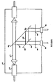
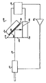
詳細説明
図1は差分検出器を用いる先行技術の波長モニター10の概念図である。光源12は光ビーム14を発生する。ビームスプリッタ16はビーム14の一部を抽出し、抽出されたビーム18を第2のビームスプリッタ20に向ける。第2のビームスプリッタ20は抽出されたビームを第1の抽出ビーム22と第2の抽出ビーム24に分割する。第2のビームスプリッタ20は第1の抽出ビーム22をローパスフィルター26に向け、第2の抽出ビーム24をハイパスフィルター28に向ける。モニター10は第2の抽出ビーム24をハイパスフィルター28に向けるためにミラー30を用いる。第1の検出器32はローパスフィルター26を透過するビームの光パワーを測定する。第2の検出器34はハイパスフィルター28を透過するビームの光パワーを測定する。
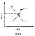
【0018】
図2は図1の先行技術の波長モニターの第1の検出器32と第2の検出器34の出力特性を表すグラフである。第1の検出器32はローパス特性36を測定する。第2の検出器34はハイパス特性38を測定する。一般的にはローパスフィルター32とハイパスフィルター34の両者の中心周波数が光源12により生ずる光ビーム14の波長と同様になるように選択される。
【0019】
動作においては光ビーム14の波長が変化すると第1の検出器32により検出される光パワーは第2の検出器34により検出される光パワーの変化に反比例する方向に変化する。従って光ビーム14の波長は第1の検出器32により検出される光パワーの第2の検出器34により検出される光パワーに対する比を測定することによりモニターできる。この比は光源12により発生される光ビームの波長変化に高感度な尺度である。しかしながらこの方法は光学モードの異なる部分を測定する光検出器を用いる。従ってこの方法では前記のようなモード不安定による測定波長の不確実に陥り易い。
【0020】
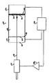
図3は本発明の波長およびパワーモニター40の一つの実施例の概念図である。モニター40は入射光ビーム42を発生する光源41を含む。入射光ビーム42の光路中にコリメータレンズ(図示せず)を配置してもよい。一つの実施例においては光源41は波長分割多重化(WDM)通信システムでの使用に適した波長可変半導体レーザである。例えば光源41は分布帰還型半導体レーザでもよい。
【0021】
モニター40はまた部分透明の第1のフォトダイオード44を含む。第1のフォトダイオード44は入射光ビーム42の光パワーに比例する第1の電気信号を発生する。光ビーム42の一部は第1のフォトダイオード44の出射面43を透過する。第1のフォトダイオード44は入射面からの反射光を低減するための入射面46上に反射防止(AR)コーティングを有していてもよい。
【0022】
第1のフォトダイオード44は少なくとも部分透明の基板48に取り付けられる。基板48はガラスで出来ていてもよい。基板48は反射光が第1のフォトダイオード44に当たって誤った信号を生じないように入射面50の上にARコーティングを有してもよい。別の実施例においてはどの反射ビームも第1のフォトダイオード44からそらし、それにより誤った信号を防止するために基板48は楔形をしている。
【0023】
モニター40はまた基板48の出射面51の上に配置される薄膜光フィルター52を含む。別の実施例においては自由空間が第1のフォトダイオード44と薄膜光フィルター52を分離し、フィルター52が光ビーム42の伝搬方向に配置される。薄膜フィルター52は狭いバンドパスフィルタでもよい。
【0024】
第2のフォトダイオード54がビーム42の伝搬方向において薄膜フィルター52に隣接して配置される。第2のフォトダイオード54は光ビーム42のフィルターされた部分の光パワーに比例する電気信号を発生する。第1のフォトダイオード44により検出されて誤った信号を生じ得る反射光を低減するために第2のフォトダイオード54は入射面56上にARコーティングを有していてもよい。
【0025】
信号処理装置58は第1および第2の電気信号を受け、光ビームを特徴づける出力信号を発生する。一つの実施例においては信号処理装置58は光ビームのフィルターされた部分の光パワーPλの、入射光ビームの光パワーPmonに対する比に比例する信号を発生する。即ち信号処理装置はPλ/Pmonに比例する信号を発生する。別の実施例においては信号処理装置はPλとPmonの差の、PλとPmonの和に対する比に比例する信号を発生する。即ち信号処理装置は(Pλ−Pmon)/(Pλ+Pmon)に比例する信号を発生する。このように本発明の一つの実施例においてはモニター40の波長伝達関数はPλ/Pmonでも(Pλ−Pmon)/(Pλ+Pmon)でもよい。
【0026】
信号処理装置58の出力信号は光源41の波長およびパワーを制御するために使用できる。一つの実施例においては光源41は波長可変レーザであり、信号処理装置58の出力は光源制御装置59に電気的に接続される。信号処理装置により発生された信号は光源制御装置59に対し光源41の波長およびパワーを変化させるようにする。
【0027】
動作においては第1のフォトダイオード44は入射光ビーム42の光パワー(Pmon)に比例する信号を発生する。第1のフォトダイオード44により吸収されなかった入射光ビームの部分は基板48を通ってフィルター52に伝搬する。フィルター52は光ビーム42の内の予め定められた帯域幅内の波長を持つ部分を透過させる。そのあと、光ビーム42のフィルターされた部分が第2のフォトダイオード54により検出される。第2のフォトダイオード54は光ビームのフィルターされた部分の光パワー(Pλ)に比例する電気信号を発生する。
【0028】
信号処理装置58は光ビームを特徴づける信号を発生する。信号はPλ/ Pmonに比例しても、(Pλ−Pmon)/ (Pλ+Pmon)に比例してもよい。信号処理装置58により発生された信号から入射ビーム42の波長と光パワーの変化をモニターできる。
【0029】
一つの実施例においてはモニター40は信号処理装置58の出力に電気的に接続される光源制御装置59を含む。光源制御装置59は信号処理装置58から信号を受け、光源41の波長とパワーを調整する。一つの実施例においては光源制御装置59は熱電冷却装置であり、光源制御装置59は光源41の温度を調整する。別の実施例においては光源制御装置59はレーザ駆動電流制御装置59であり、光源制御装置59は光源41の駆動電流を調整する。
【0030】
図4は本発明の波長およびパワーモニター60の別の実施例の概念図である。モニター60は図3に関連して説明したモニター40に類似している。モニター60は部分透明の第1のフォトダイオード44を含む。第1のフォトダイオード44は入射光ビーム42の光パワーに比例する第1の電気信号を発生する。第1のフォトダイオード44は入射面からの反射光を低減するために入射面46上にARコーティングを有していてもよい。
【0031】
モニター60は基板を有していない。その代わりモニター60は光ビーム42の伝搬方向において第1のフォトダイオード44に直接隣接して配置される薄膜光フィルター52を含む。薄膜フィルター52は狭いバンドパスフィルターでもよい。第2のフォトダイオード54は光ビーム42の伝搬方向において薄膜フィルター52に隣接して配置される。第2のフォトダイオード54は光ビーム42のフィルターされた部分の光パワーに比例する電気信号を発生する。第2のフォトダイオード54は第1のフォトダイオード44により検出され得る反射光を低減するために入射面56上にARコーティングを有していてもよい。
【0032】
信号処理装置58は第1および第2の電気信号を受け、光ビームを特徴づける出力信号を発生する。本発明の一つの実施例においては信号処理装置58はPλ/Pmonまたは(Pλ−Pmon)/(Pλ+Pmon)に比例する信号を発生する。信号処理装置58により発生された信号から入射ビーム42の波長および光パワーの変化をモニターできる。一つの実施例においてはモニター60は信号処理装置58の出力に電気的に結合される光源制御装置59を含む。光源制御装置59は図3に関連して説明したように光源41の波長およびパワーを制御する。モニター60の動作は図3に関連して説明したモニター40の動作と同様である。
【0033】
図5はバルクのファブリーペロー(FP)フィルターを含む本発明の波長およびパワーモニター70の別の実施例の概念図である。モニター70は図3に関連して説明したモニター40に類似している。モニター70は部分透明の第1のフォトダイオード44を含む。第1のフォトダイオード44は入射光ビーム42の光パワーに比例する第1の電気信号を発生する。第1のフォトダイオード44は入射面からの反射光を低減するために入射面46上にARコーティングを有していてもよい。
【0034】
モニター70は光ビーム42の伝搬方向において第1のフォトダイオード44に隣接して配置されるバルクのファブリーペローフィルター49を含む。ファブリーペローフィルター49は第1のフォトダイオード44に隣接する一つの端部に配置された第1の部分反射ミラー71と第2の端部に配置された第2の部分反射ミラー72とを有する。ファブリーペローフィルター49は周期的な櫛状の透過率と反射率を発生する。
【0035】
第2のフォトダイオード54はビーム42の伝搬方向においてファブリーペローフィルター49に隣接して配置される。第2のフォトダイオード54は光ビーム42のフィルターされた部分の光パワーに比例する電気信号を発生する。第2のフォトダイオード54は第1のフォトダイオード44に検出され得る反射光を低減するために入射面56上にARコーティングを有していてもよい。
【0036】
信号処理装置58は第1および第2の電気信号を受け、光ビームを特徴づける出力信号を発生する。信号処理装置58はPλ/Pmonに比例する信号を発生してもよいし、(Pλ−Pmon)/(Pλ+Pmon)に比例する信号を発生してもよい。一つの実施例においてはモニター70は信号処理装置58の出力に電気的に結合される光源制御装置59を含む。光源制御装置59は図3に関連して説明したように光源41の波長およびパワーを制御する。
【0037】
図6はビームスプリッタ90を含む本発明の波長およびパワーモニター75の別の実施例の概念図である。一つの実施例においてはビームスプリッタ90は無偏光ビームスプリッタにより構成される。ビームスプリッタ90は入射ビーム42の伝搬方向にビームの一部を透過し、入射ビーム42の伝搬方向に垂直な方向にビームの一部を反射する斜辺98上に付着された部分反射ミラーを含む。ビームスプリッタ90は入射面92と出射面94の少なくとも一方に付着されたARコーティングを有していてもよい。
【0038】
モニター75は入射ビーム42の伝搬方向に垂直な方向に配置される第1のフォトダイオード44を含む。第1のフォトダイオード44は入射光ビーム42の光パワーに比例する電気信号を発生する。第1のフォトダイオード44は入射面からの反射光を低減するために入射面上にARコーティングを有していてもよい。
【0039】
薄膜フィルター52はビーム42の伝搬方向に配置される。第2のフォトダイオード54はビーム42の伝搬方向において薄膜フィルター52に隣接して配置される。第2のフォトダイオード54は光ビーム42のフィルターされた部分の光パワーに比例する電気信号を発生する。第2のフォトダイオード54は第1のフォトダイオード44により検出され得る反射光を低減するためにARコーティングを有していてもよい。薄膜フィルター52はビームスプリッタ90に付着されても、フォトダイオード54に付着されてもよいし、ビームスプリッタ90とフォトダイオード54の間に配置されてもよい。
【0040】
信号処理装置58は第1および第2の電気信号を受け、光ビームを特徴づける出力信号を発生する。モニター75の動作は本発明のモニターの他の実施例の動作と同様である。信号処理装置58はPλ/Pmonに比例する信号を発生してもよいし、(Pλ−Pmon)/(Pλ+Pmon)に比例する信号を発生してもよい。一つの実施例においてはモニター75は信号処理装置58の出力に電気的に結合される光源制御装置59を含む。光源制御装置59は図3に関連して説明したように光源41の波長とパワーを制御する。
【0041】
本発明のモニターはビームスプリッタを用いる多数の他の実施例を有する。例えばモニターの一つの実施例(図示せず)においては第1のフォトダイオードが入射ビームの伝搬方向においてビームスプリッタの後に配置される。薄膜フィルターと第2のフォトダイオードが入射ビームに垂直な方向においてビームスプリッタの後に配置される。この実施例の動作は図6のモニターの動作と同様になり、この実施例の波長伝達関数もまた(Pλ/Pmon)で表しても、(Pλ−Pmon)/(Pλ+Pmon)で表してもよい。ここでPmonはフォトダイオードの出力電気信号に比例し、Pλは第2のフォトダイオードの出力に比例する。
【0042】
図7はガラス楔102を含む本発明の波長およびパワーモニター100の別の実施例の概念図である。ガラス楔102は図6のビームスプリッタ90に類似している。ガラス楔102は入射ビーム42の伝搬方向にビームの一部を透過し、入射ビーム42の伝搬方向に垂直な方向にビームの一部を反射する。
【0043】
モニター100は入射ビーム42の伝搬方向に垂直に配置される第1のフォトダイオード44を含む。第1のフォトダイオード44は入射光ビーム42の光パワーに比例する第1の電気信号を発生する。第1のフォトダイオード44は入射面からの反射光を低減するために入射面上にARコーティングを有していてもよい。
【0044】
薄膜フィルター52はガラス楔の斜面98に蒸着又は配置される。第2のフォトダイオード54はビーム42の伝搬方向において薄膜フィルター52に隣接して配置される。第2のフォトダイオード54は光ビーム42のフィルターされた部分の光パワーに比例する電気信号を発生する。第2のフォトダイオード54は第1のフォトダイオード44により検出され得る反射光を低減するためにARコーティングを有していてもよい。
【0045】
信号処理装置58は第1および第2の電気信号を受け、光ビームを特徴づける出力信号を発生する。モニター75の動作は本発明のモニターの他の実施例の動作と同様である。信号処理装置58はPλ/Pmonに比例する信号を発生してもよいし、(Pλ−Pmon)/(Pλ+Pmon)に比例する信号を発生してもよい。一つの実施例においてはモニター60は信号処理装置58の出力に電気的に結合される光源制御装置59を含む。光源制御装置59は図3に関連して説明したように光源41の波長とパワーを制御する。
【0046】
図8はファブリーペローフィルター49とビームスプリッタ90をもつガラス基板を含む本発明の波長およびパワーモニター150の別の実施例の概念図である。ビームスプリッタ90は入射ビーム42の伝搬方向にビームの一部を透過し、入射ビーム42の伝搬方向に垂直な方向にビームの一部を反射する斜面98の上に付着された部分反射ミラーを有する。ビームスプリッタ90は入射面92と出射面94の少なくとも一方に付着されたARコーティングを有していてもよい。
【0047】
バルクのファブリーペローフィルター49が入射ビーム42の伝搬方向に配置される。ファブリーペローフィルター49は入射端に配置された第1の部分反射ミラー71と出口に配置された第2の部分反射ミラー72を有する。ファブリーペローフィルター49は周期的な櫛状の透過率および反射率を生ずる。
【0048】
モニター150は入射ビーム42の伝搬方向に垂直に配置された第1のフォトダイオード44を含む。第1のフォトダイオード44は入射光ビーム42の光パワーに比例する第1の電気信号を発生する。第1のフォトダイオード44は入射面からの反射光を低減するために入射面上にARコーティングを有していてもよい。第1のフォトダイオード44により検出された光パワーはファブリーペローフィルター49から反射されたビームに依存しない。
【0049】
モニター150は入射ビームの伝搬方向においてファブリーペローフィルター49に隣接して配置される第2のフォトダイオード54を含む。第2のフォトダイオード54は入射ビーム42のフィルターされた部分の光パワーに比例する電気信号を発生する。
【0050】
信号処理装置58は第1および第2の電気信号を受け、光ビーム42を特徴づける出力信号を発生する。モニター150の動作は本発明のモニターの他の実施例の動作と同様である。信号処理装置58はPλ/Pmonに比例する信号を発生してもよいし、(Pλ−Pmon)/(Pλ+Pmon)に比例する信号を発生してもよい。一つの実施例においてはモニター150は信号処理装置58の出力に電気的に結合される光源制御装置59を含む。光源制御装置59は図3に関連して説明したように光源41の波長とパワーを制御する。
【0051】
図9は粗い波長モニター用広帯域薄膜フィルターと、細かい波長モニター用ファブリーペローエタロンとを含む本発明の広帯域波長およびパワーモニター200の概念図である。モニター200は光ビーム42を発生する、波長可変半導体レーザのような光源41を含む。入射光ビーム42の光路中にコリメータレンズ(図示せず)を配置してもよい。
【0052】
ビームスプリッタ90が光ビーム42の光路中に配置される。一つの実施例においてはビームスプリッタ90は無偏光ビームスプリッタにより構成される。ビームスプリッタ90は入射ビーム42の伝搬方向にビームの一部を透過し、入射ビーム42の伝搬方向に垂直な方向にビームの一部を反射する斜面98の上に付着された部分反射ミラーを含む。ビームスプリッタ90は入射面92と出射面94の少なくとも一方に付着されたARコーティングを有していてもよい。
【0053】
モニター200は入射ビーム42の伝搬方向に垂直な方向のビームの部分の光路中に配置される第2のビームスプリッタ202を含む。第2のビームスプリッタ202はビームの反射された部分を第1の光路204と第2の光路206に分割する。一つの実施例においては第2のビームスプリッタ202はシリンドリカルレンズである。
【0054】
第1のフォトダイオード208が第1の光路204中に配置される。第1のフォトダイオード208は入射光ビーム42の光パワーに比例する第1の電気信号を発生する。第1のフォトダイオード208は入射面209からの反射光を低減するために入射面209の上にARコーティングを有していてもよい。
【0055】
粗いフィルター210が第2の光路206中に配置される。一つの実施例においては粗いフィルター210は薄膜フィルターにより構成される。粗いフィルター210は比較的広帯域の光信号を通す。第2のフォトダイオード212が第2の光路206中に粗いフィルター210の後に配置される。第2のフォトダイオード212は広帯域光信号の光パワーに比例する第2の電気信号を発生する。
【0056】
ファブリーペローエタロン214が入射ビーム42の伝搬方向に配置される。ファブリーペローエタロンあるいはファブリーペロー干渉計はファブリーペローエタロン214の多数の光路に対応する多数の波長を有する光信号を通す比較的細い波長の、あるいは狭帯域のフィルターである。第3のフォトダイオード216が入射ビーム42の伝搬方向においてファブリーペローエタロン214の後に配置される。第3のフォトダイオード216はファブリーペローエタロン214の多数の光路に対応する多数の波長を検出し、ファブリーペローエタロン214により透過されたビームの光パワーに比例する第3の電気信号を発生する。
【0057】
信号処理装置58は第1、第2、第3の電気信号を受け、光ビーム42を特徴づける出力信号を発生する。信号処理装置58はPλ/Pmonに比例する信号を発生してもよいし、(Pλ−Pmon)/(Pλ+Pmon)に比例する信号を発生してもよい。一つの実施例においてはモニター200は信号処理装置58の出力に電気的に結合される光源制御装置59を含む。光源制御装置59は図3に関連して説明したように光源41の波長およびパワーを制御する。
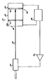
【0058】
図10は波長可変レーザ254の出力を制御するための本発明の波長およびパワーモニター252を含む光通信システム250の概念図である。波長可変レーザ254は光変調器256に光学的に結合される。光変調器256は波長可変レーザ254の出力を変調し、変調された光ビームを発生する。一つの実施例においては変調された光ビームは光通信システムの光ファイバーに結合される。変調されたビームの一部は波長およびパワーモニター252に結合される。一つの実施例においては変調器はマッハツェンダー干渉計であり波長およびパワーモニター252は干渉計の第2のポートに光学的に結合される。
【0059】
波長およびパワーモニター252は本発明に従うどのようなモニターであってもよい。例えばモニター252は図9に関連して説明した広帯域モニターであってもよい。この実施例ではモニター252は第1、第2、第3の電気信号を発生する。信号処理装置258は第1、第2、第3の電気信号を受け、光ビーム42を特徴づける信号を出力において発生する。
【0060】
信号処理装置258の出力は波長可変レーザ制御装置260の入力に電気的に結合される。波長可変レーザ制御装置260は信号処理装置により発生された信号を受け、レーザの光パワーおよび波長を制御する。一つの実施例においては波長可変レーザ制御装置260は熱電冷却装置であり、それはレーザの温度を制御することにより波長可変レーザ254を制御する。別の実施例においては波長可変レーザ制御装置260はレーザ駆動電流制御装置でありレーザの駆動電流を変化することにより波長可変レーザ254を制御する。
【0061】
本発明の波長およびパワーモニターは先行技術のモニターに対して多数の利点を有している。一つの利点は本発明のモニターが単一光ビームのモードの一つの部分をモニターし、単一光ビームの波長と光パワーを実質的に同時に決定することである。単一光ビームのモードの一つの部分をモニターすることは前記の差分検出に関連する問題を回避する。本発明のモニターはビームの同一部分を抽出するのでモニターされる光源のモード安定性に影響されにくい。この特徴はモニターの長期安定性を改善する。この特徴はまた半導体レーザを定電流モードではなく定パワーモードで動作することを可能にする。これは半導体レーザのモード構造がレーザの注入電流に依存するからである。
【0062】
同等性
発明は具体的な好ましい実施例に言及して詳細に示され、また説明されたが、添付された請求範囲により定義される発明の精神および範囲から逸脱することなく形態および詳細における種々の変更を成し得ることは当業者には言うまでもない。
【図面の簡単な説明】
【図1】差分検出を用いる先行技術の波長モニターの概念図である。
【図2】図1の先行技術の波長モニターの第1および第2の検出器の出力特性を表すグラフである。
【図3】本発明の波長およびパワーモニターの一つの実施例の概念図である。
【図4】基板を含まない本発明の波長およびパワーモニターの別の実施例の概念図である。
【図5】ファブリーペローフィルターを含む本発明の波長およびパワーモニターの別の実施例の概念図である。
【図6】ビームスプリッタを含む本発明の波長およびパワーモニターの一つの実施例の概念図である。
【図7】ガラス楔を含む本発明の波長およびパワーモニターの別の実施例の概念図である。
【図8】ファブリーペローフィルター付きのガラス基板とビームスプリッタを含む本発明の波長およびパワーモニターの別の実施例の概念図である。
【図9】粗い波長モニター用の広帯域薄膜フィルターと細かい波長モニター用のファブリーペローエタロンを含む本発明の広帯域波長およびパワーモニターの概念図である。
【図10】波長可変レーザの出力を制御するための本発明の波長およびパワーモニターを含む光通信システムの概念図である。[0001]
Field of the invention
The present invention relates to optical signal monitoring, and more particularly, to an apparatus and method for monitoring the wavelength and power of an optical communication signal.
[0002]
Background of the Invention
Modern fiber optic communication systems have a wide bandwidth and low transmission loss. The bandwidth of an optical fiber determines how much information can be transmitted without data loss due to degradation of the optical signal. Many modern fiber optic communication systems use wavelength division multiplexing (WDM).
[0003]
In a WDM communication system, separate signals having different carrier wavelengths are transmitted simultaneously in a single optical fiber. The number of wavelengths that propagate simultaneously in the fiber is proportional to the communication system bandwidth. Each wavelength bandwidth occupies a fixed channel spacing in the communication system. The closer the spacing between carrier wavelengths, the more channels that can be propagated simultaneously. However, the smaller the spacing between wavelengths, the greater the possibility of crosstalk between channels. This crosstalk causes data from one channel to interfere with data from another channel, thereby causing erroneous data propagation in the communication system and ultimately disrupting the data at the receiving end.
[0004]
In order to maximize the number of channels available in a WDM communication system, each laser source must generate a light beam having a relatively stable wavelength. Lasers used in WDM transmitters generally emit light of a stable wavelength, and the wavelength can be precisely controlled. However, many laser light sources experience a temporal drift in wavelength caused by temperature, aging, and mode instability. The wavelength drift can cause crosstalk, which can result in data loss in a WDM communication system, which must be monitored and compensated.
[0005]
A number of devices and methods have been used to monitor the wavelength of an optical signal in a WDM communication system. Some of these devices and methods separate the input signal into two signals, filter one signal with a low-pass filter, and filter the other signal with a high-pass filter. The filtered signal is directed to two closely spaced detectors. The electrical signals generated by the two detectors are then compared. By properly selecting the characteristics of the filter, the wavelength of the optical signal can be precisely determined and monitored.
[0006]
Other devices and methods used to monitor the wavelength of an optical signal in a WDM communication system use a channel selector, such as a crystal or diffraction grating, and a wavemeter to monitor the optical signal. For example, in some prior art, an optical signal is first separated into channels by a channel selector and then propagated to a wavemeter that monitors the wavelength of the optical signal in each channel.
[0007]
Because these prior art wavelength monitors are complex and occupy a large volume, they are generally not practical for modern high capacity optical communication systems. Further, these prior art wavelength monitors use differential detection to measure the wavelength of the communication signal, which can result in erroneous measurements. These difference detection methods require at least two photodetectors to extract different parts of the waveguide mode.
[0008]
Measuring two different parts of a waveguide mode can lead to uncertainty of the measured wavelength due to mode instability. These uncertainties can result in erroneous measurements and erroneous compensation. If the waveguide is a single mode optical fiber, the modes are typically very stable. However, if the waveguide is multimode, mode instability exists under some conditions. There are several factors that cause mode instability in the propagation medium. These factors include injection current level, facet coating conditions, efficiency and operating temperature.
[0009]
Summary of the Invention
The present invention relates to wavelength and power monitoring and does not suffer from the disadvantages of differential detection and prior art wavelength monitoring methods. The principal finding of the present invention is that the light wavelength and power monitor is configured to monitor one part of the modes of a single light beam, and that the wavelength and light power of a single light beam can be determined substantially simultaneously. .
[0010]
Accordingly, the invention features a light beam monitor that includes a first detector disposed in the light path of the light beam. In one example, the first detector comprises a translucent light detector that transmits a portion of the light beam. The first detector includes an anti-reflective coating that prevents a portion of the light beam from being reflected from the first detector. The first detector generates an electrical signal proportional to the optical power of the incident light beam.
[0011]
An optical filter, such as a Fabry-Perot filter or a thin film filter, is placed in the optical path of the light beam and passes a portion of the light beam corresponding to a wavelength within the bandwidth of the optical filter. In one example, the optical filter comprises a narrow bandpass filter. The substrate may be located between the first detector and the light filter. In one example, the substrate is formed of glass. In one example, the substrate has an anti-reflective coating applied to at least one end of the substrate to prevent reflection. In another example, a glass wedge is positioned between the first detector and the optical filter to divert any reflected beams from the first detector, thereby reducing false signal detection. The glass wedge may have an antireflection film for preventing reflection.
[0012]
A second detector is located in the optical path of the light beam. The second detector generates a second electrical signal that is proportional to the optical power of the filtered light beam. A processing unit is coupled to the first and second detectors and is used to generate a signal characterizing the wavelength and power of the light beam. This signal can be used to control the wavelength and power of the light source generating the light beam.
[0013]
The invention also features an apparatus for monitoring the power and wavelength of an optical signal in a wavelength division multiplex communication system. The device includes a multi-wavelength laser that generates a light beam. The first detector is located in the optical path of the light beam. The first detector generates an electrical signal proportional to the optical power of the light beam propagating in the communication system. An optical filter is located in the optical path of the light beam. The optical filter transmits a portion of the light beam corresponding to a channel of the communication system.
[0014]
A second detector is located in the optical path of the light beam. A second detector generates a second electrical signal corresponding to the channel and proportional to the optical power of the filtered light beam. The signal processing device receives the first and second electrical signals. The signal processing device generates at least one signal corresponding to the wavelength and power of the light beam propagating in the communication system. This signal can be used to control the wavelength and power of the multi-wavelength laser.
[0015]
The invention also features a method of monitoring the wavelength and power of a light beam. The method includes detecting a light beam and generating a first electrical signal corresponding to an optical power of the light beam. The portion of the light beam having a wavelength within the predetermined bandwidth is then detected. A second electrical signal is generated corresponding to the optical power of the portion of the light beam within the predetermined bandwidth. The first and second electrical signals are processed to generate a signal characterizing the light beam. In one example, this signal controls the light source that generates the light beam.
[0016]
The above and other objects, features and advantages of the present invention, and the manner of realizing them, will be understood from a review of the following description and the appended claims, taken in conjunction with the accompanying drawings which illustrate some of the many embodiments of the invention. It will be clear and understood.
[0017]
Detailed explanation
FIG. 1 is a conceptual diagram of a prior art wavelength monitor 10 using a difference detector. The light source 12 generates a light beam 14. Beam splitter 16 extracts a portion of beam 14 and directs extracted
[0018]
FIG. 2 is a graph showing the output characteristics of the
[0019]
In operation, when the wavelength of the light beam 14 changes, the light power detected by the
[0020]
FIG. 3 is a conceptual diagram of one embodiment of the wavelength and power monitor 40 of the present invention. Monitor 40 includes a light source 41 that generates an
[0021]
Monitor 40 also includes a partially transparent first photodiode 44. First photodiode 44 generates a first electrical signal proportional to the optical power of
[0022]
The first photodiode 44 is mounted on a substrate 48 that is at least partially transparent. Substrate 48 may be made of glass. Substrate 48 may have an AR coating on
[0023]
Monitor 40 also includes a thin-film
[0024]
A second photodiode 54 is arranged adjacent to the thin-
[0025]
[0026]
The output signal of the
[0027]
In operation, the first photodiode 44 applies the optical power (P mon ). The portion of the incident light beam that has not been absorbed by the first photodiode 44 propagates through the substrate 48 to the
[0028]
[0029]
In one embodiment, monitor 40 includes a
[0030]
FIG. 4 is a conceptual diagram of another embodiment of the wavelength and power monitor 60 of the present invention.
[0031]
The
[0032]
[0033]
FIG. 5 is a conceptual diagram of another embodiment of the wavelength and power monitor 70 of the present invention including a bulk Fabry-Perot (FP) filter. Monitor 70 is similar to monitor 40 described in connection with FIG. Monitor 70 includes a partially transparent first photodiode 44. First photodiode 44 generates a first electrical signal proportional to the optical power of
[0034]
Monitor 70 includes a bulk Fabry-Perot filter 49 disposed adjacent to first photodiode 44 in the direction of propagation of
[0035]
The second photodiode 54 is arranged adjacent to the Fabry-Perot filter 49 in the propagation direction of the
[0036]
[0037]
FIG. 6 is a conceptual diagram of another embodiment of the wavelength and power monitor 75 including the
[0038]
The monitor 75 includes a first photodiode 44 arranged in a direction perpendicular to the propagation direction of the
[0039]
The
[0040]
[0041]
The monitor of the present invention has a number of other embodiments using a beam splitter. For example, in one embodiment of the monitor (not shown), a first photodiode is located after the beam splitter in the direction of propagation of the incident beam. A thin film filter and a second photodiode are located after the beam splitter in a direction perpendicular to the incident beam. The operation of this embodiment is similar to that of the monitor of FIG. 6, and the wavelength transfer function of this embodiment is also (P λ / P mon ), (P λ −P mon ) / (P λ + P mon ). Where P mon Is proportional to the output electric signal of the photodiode, and P λ Is proportional to the output of the second photodiode.
[0042]
FIG. 7 is a conceptual diagram of another embodiment of the wavelength and power monitor 100 of the present invention including a
[0043]
Monitor 100 includes a first photodiode 44 arranged perpendicular to the direction of propagation of
[0044]
The
[0045]
[0046]
FIG. 8 is a conceptual diagram of another embodiment of the wavelength and power monitor 150 of the present invention including a glass substrate having a Fabry-Perot filter 49 and a
[0047]
A bulk Fabry-Perot filter 49 is arranged in the propagation direction of the
[0048]
Monitor 150 includes a first photodiode 44 arranged perpendicular to the direction of propagation of
[0049]
Monitor 150 includes a second photodiode 54 disposed adjacent to Fabry-Perot filter 49 in the direction of propagation of the incident beam. The second photodiode 54 produces an electrical signal proportional to the optical power of the filtered portion of the
[0050]
[0051]
FIG. 9 is a conceptual diagram of a broadband wavelength and power monitor 200 of the present invention including a coarse wavelength monitor broadband thin film filter and a fine wavelength monitor Fabry-Perot etalon.
[0052]
A
[0053]
[0054]
A
[0055]
A
[0056]
A Fabry-
[0057]
[0058]
FIG. 10 is a conceptual diagram of an
[0059]
Wavelength and power monitor 252 may be any monitor according to the present invention. For example, monitor 252 may be the broadband monitor described in connection with FIG. In this embodiment, monitor 252 generates first, second, and third electrical signals.
[0060]
The output of
[0061]
The wavelength and power monitor of the present invention has a number of advantages over prior art monitors. One advantage is that the monitor of the present invention monitors one portion of the mode of a single light beam and determines the wavelength and optical power of the single light beam substantially simultaneously. Monitoring one portion of the mode of a single light beam avoids the problems associated with differential detection described above. Because the monitor of the present invention extracts the same portion of the beam, it is less sensitive to the mode stability of the monitored light source. This feature improves the long-term stability of the monitor. This feature also allows the semiconductor laser to operate in a constant power mode instead of a constant current mode. This is because the mode structure of the semiconductor laser depends on the injection current of the laser.
[0062]
Equivalence
Although the invention has been shown and described in detail with reference to specific preferred embodiments, various changes in form and detail can be made without departing from the spirit and scope of the invention as defined by the appended claims. What can be achieved will be apparent to those skilled in the art.
[Brief description of the drawings]
FIG. 1 is a conceptual diagram of a prior art wavelength monitor using difference detection.
FIG. 2 is a graph illustrating the output characteristics of first and second detectors of the prior art wavelength monitor of FIG.
FIG. 3 is a conceptual diagram of one embodiment of the wavelength and power monitor of the present invention.
FIG. 4 is a conceptual diagram of another embodiment of the wavelength and power monitor of the present invention that does not include a substrate.
FIG. 5 is a conceptual diagram of another embodiment of the wavelength and power monitor of the present invention including a Fabry-Perot filter.
FIG. 6 is a conceptual diagram of one embodiment of a wavelength and power monitor of the present invention including a beam splitter.
FIG. 7 is a conceptual diagram of another embodiment of the wavelength and power monitor of the present invention including a glass wedge.
FIG. 8 is a conceptual diagram of another embodiment of the wavelength and power monitor of the present invention including a glass substrate with a Fabry-Perot filter and a beam splitter.
FIG. 9 is a conceptual diagram of a broadband wavelength and power monitor of the present invention including a broadband thin film filter for coarse wavelength monitoring and a Fabry-Perot etalon for fine wavelength monitoring.
FIG. 10 is a conceptual diagram of an optical communication system including a wavelength and power monitor of the present invention for controlling the output of a tunable laser.
Claims (23)
b.前記光ビームの光路中に配置された光フィルターであって該光フィルターの帯域幅内の波長を有する光ビームの部分を透過する光フィルターと;
c.前記光ビームの前記光路中に配置され、前記フィルターされた光ビームの光パワーに比例する第2の電気信号を発生する第2の検出器と;
d.前記第1および第2の電気信号を受け、前記光ビームを特徴づける信号を発生する信号処理装置と;を備えた光ビームモニター。a. A first detector disposed in the optical path of the light beam and generating a first electrical signal proportional to the optical power of the light beam;
b. An optical filter disposed in an optical path of the light beam, the optical filter transmitting a portion of the light beam having a wavelength within a bandwidth of the optical filter;
c. A second detector disposed in the optical path of the light beam for generating a second electrical signal proportional to the optical power of the filtered light beam;
d. A signal processor that receives the first and second electrical signals and generates a signal characterizing the light beam.
a.光ビームの光路中に配置され、前記通信システム中を伝搬する光ビームの光パワーに比例する第1の電気信号を発生する第1の検出器と;
b.光ビームの光路中に配置され、前記通信システムのチャンネルに対応する光ビームのフィルターされた部分を透過する光フィルターと;
c.光ビームの光路中に配置され、前記通信システムのチャンネルに対応する光ビームの前記フィルターされた部分の光パワーに比例する第2の電気信号を発生する第2の検出器と;
d.前記第1および第2の電気信号を受け、前記通信システム中を伝搬する光ビームの波長に比例する信号とパワーに比例する信号の少なくとも一つの信号を発生する信号処理装置と;を備えた光ビームモニター。An optical beam monitor for simultaneously monitoring the optical power and wavelength of an optical signal in a wavelength division multiplexing communication system,
a. A first detector disposed in the optical path of the light beam and generating a first electrical signal proportional to the optical power of the light beam propagating in the communication system;
b. An optical filter disposed in an optical path of the light beam and transmitting a filtered portion of the light beam corresponding to a channel of the communication system;
c. A second detector disposed in the optical path of the light beam and generating a second electrical signal proportional to the optical power of the filtered portion of the light beam corresponding to a channel of the communication system;
d. A signal processing device that receives the first and second electric signals and generates at least one signal of a signal proportional to a wavelength of a light beam propagating in the communication system and a signal proportional to the power of the light beam Beam monitor.
b.広帯域フィルターされた光ビーム光路中に配置され、通信システムの前記少なくとも二つのチャンネルに対応するビームの前記広帯域フィルターされた部分の光パワーに比例する第3の電気信号を発生する第3の検出器と;を備え、
信号処理装置が第1と第2と第3の電気信号を受けて前記通信システム中を伝搬する前記光ビームの波長に比例する信号とパワーに比例する信号の少なくとも一つの信号を発生することを特徴とする請求項17記載の光ビームモニター。a. A second optical filter disposed in the optical path of the light beam and transmitting a broadband filtered portion of the light beam corresponding to at least two channels of the communication system;
b. A third detector disposed in the broadband filtered light beam path for generating a third electrical signal proportional to the optical power of the broadband filtered portion of the beam corresponding to the at least two channels of the communication system; And;
A signal processor receiving the first, second and third electrical signals and generating at least one of a signal proportional to a wavelength of the light beam and a signal proportional to the power of the light beam propagating in the communication system; The light beam monitor according to claim 17, characterized in that:
b.予め定められた帯域幅内の波長を有する光ビームの部分を検出し、前記予め定められた帯域幅内の波長を有する光ビームの部分の光パワーに比例する第2の電気信号を発生するステップと;
c.前記第1および第2の電気信号を処理して前記光ビームを特徴づける信号を発生するステップと;を含む光ビームの光パワーおよび波長をモニターする方法。a. Detecting a light beam and generating a first electrical signal proportional to the light power of the light beam;
b. Detecting a portion of the light beam having a wavelength within a predetermined bandwidth and generating a second electrical signal proportional to the optical power of the portion of the light beam having a wavelength within the predetermined bandwidth. When;
c. Processing the first and second electrical signals to generate a signal characterizing the light beam; and monitoring the light power and wavelength of the light beam.
Applications Claiming Priority (2)
| Application Number | Priority Date | Filing Date | Title |
|---|---|---|---|
| US09/603,403 US6587214B1 (en) | 2000-06-26 | 2000-06-26 | Optical power and wavelength monitor |
| PCT/US2001/020224 WO2002001765A2 (en) | 2000-06-26 | 2001-06-25 | Optical power and wavelength monitor |
Publications (2)
| Publication Number | Publication Date |
|---|---|
| JP2004502141A true JP2004502141A (en) | 2004-01-22 |
| JP2004502141A5 JP2004502141A5 (en) | 2005-01-06 |
Family
ID=24415285
Family Applications (1)
| Application Number | Title | Priority Date | Filing Date |
|---|---|---|---|
| JP2002505420A Pending JP2004502141A (en) | 2000-06-26 | 2001-06-25 | Optical power and wavelength monitor |
Country Status (5)
| Country | Link |
|---|---|
| US (1) | US6587214B1 (en) |
| EP (1) | EP1236293A2 (en) |
| JP (1) | JP2004502141A (en) |
| CA (1) | CA2381793A1 (en) |
| WO (1) | WO2002001765A2 (en) |
Cited By (1)
| Publication number | Priority date | Publication date | Assignee | Title |
|---|---|---|---|---|
| WO2023037510A1 (en) * | 2021-09-10 | 2023-03-16 | 三菱電機株式会社 | Wavelength locker, monitor photodiode, beam splitter, and method for aligning wavelength locker |
Families Citing this family (32)
| Publication number | Priority date | Publication date | Assignee | Title |
|---|---|---|---|---|
| JP2001284711A (en) * | 2000-03-31 | 2001-10-12 | Hitachi Ltd | Optical transmission device and optical system using it |
| JP3999122B2 (en) * | 2000-09-08 | 2007-10-31 | 富士通株式会社 | Optical transmission equipment |
| JP3781982B2 (en) * | 2000-12-06 | 2006-06-07 | 三菱電機株式会社 | Semiconductor laser device |
| US6856400B1 (en) | 2000-12-14 | 2005-02-15 | Luna Technologies | Apparatus and method for the complete characterization of optical devices including loss, birefringence and dispersion effects |
| JP2002214049A (en) * | 2001-01-17 | 2002-07-31 | Ando Electric Co Ltd | Wavelength monitor |
| US6788422B2 (en) * | 2001-04-17 | 2004-09-07 | Zygo Corporation | Method and apparatus for using quasi-stable light sources in interferometry applications |
| US7061947B2 (en) * | 2001-11-01 | 2006-06-13 | Agility Communications, Inc. | Partially mirrored beam tap for wavelength lockers |
| US6959024B2 (en) * | 2002-02-28 | 2005-10-25 | Picarro, Inc. | Laser Tuning by spectrally dependent spatial filtering |
| US6888854B2 (en) * | 2002-07-03 | 2005-05-03 | Lambda Crossing Ltd. | Integrated monitor device |
| WO2004005974A2 (en) * | 2002-07-09 | 2004-01-15 | Luna Technologies | Heterodyne optical spectrum analyzer |
| US7212555B2 (en) * | 2002-11-01 | 2007-05-01 | Finisar Corporation | Methods and devices for monitoring the wavelength and power of a laser |
| US6859284B2 (en) * | 2002-12-02 | 2005-02-22 | Picarro, Inc. | Apparatus and method for determining wavelength from coarse and fine measurements |
| US7304748B2 (en) * | 2003-06-26 | 2007-12-04 | Cymer, Inc. | Method and apparatus for bandwidth measurement and bandwidth parameter calculation for laser light |
| US7422377B2 (en) * | 2003-06-30 | 2008-09-09 | Finisar Corporation | Micro-module with micro-lens |
| US20050025420A1 (en) * | 2003-06-30 | 2005-02-03 | Mina Farr | Optical sub-assembly laser mount having integrated microlens |
| US7133136B2 (en) * | 2003-10-22 | 2006-11-07 | Jds Uniphase Corporation | Wavelength monitor |
| US7348530B2 (en) * | 2004-10-05 | 2008-03-25 | Avago Technologies Ecbu Ip Pte Ltd | System, method and apparatus for regulating the light emitted by a light source |
| GB2420848A (en) * | 2004-11-30 | 2006-06-07 | Bookham Technology Plc | Compact optical wavelength monitoring device |
| US20060171649A1 (en) * | 2005-01-31 | 2006-08-03 | Finisar Corporation | Wavelength monitoring and stabilization in wavelength division multiplexed systems |
| JP4247693B2 (en) * | 2006-11-20 | 2009-04-02 | ソニー株式会社 | Projection display |
| CN102243102B (en) * | 2011-04-25 | 2014-09-03 | 浙江中欣动力测控技术有限公司 | Photoelectric measuring device capable of measuring power and wavelength at same time |
| CN102243101A (en) * | 2011-04-25 | 2011-11-16 | 宁波诺驰光电科技发展有限公司 | Light power measuring device with wavelength recognizing function |
| US9369201B2 (en) * | 2012-04-23 | 2016-06-14 | Oracle International Corporation | Integrated multi-channel wavelength monitor |
| CN102661788B (en) * | 2012-05-30 | 2017-04-19 | 上海奥通激光技术有限公司 | Laser energy detector |
| US9172462B2 (en) * | 2012-12-31 | 2015-10-27 | Zephyr Photonics Inc. | Optical bench apparatus having integrated monitor photodetectors and method for monitoring optical power using same |
| US9490899B1 (en) * | 2013-05-17 | 2016-11-08 | The United States Of America As Represented By The Administrator Of National Aeronautics And Space Administration | Optical tunable-based transmitter for multiple radio frequency bands |
| EP2995979B1 (en) * | 2013-05-27 | 2018-11-14 | Huawei Technologies Co., Ltd. | Filter and manufacturing method thereof, and laser wavelength monitoring device |
| KR101743276B1 (en) | 2014-11-26 | 2017-06-15 | 한국전자통신연구원 | Optical wave and power measurement device |
| US11309973B2 (en) * | 2018-01-31 | 2022-04-19 | Nokia Solutions And Networks Oy | Optical burst monitoring |
| US10775149B1 (en) | 2018-03-14 | 2020-09-15 | Onto Innovation Inc. | Light source failure identification in an optical metrology device |
| US11329722B2 (en) | 2020-03-27 | 2022-05-10 | Relative Dynamics Incorporated | Optical terminals |
| TWI735194B (en) | 2020-03-30 | 2021-08-01 | 國立臺灣科技大學 | Wavelength tunable bidirectional optical wireless communication system based on self-injection lock |
Family Cites Families (22)
| Publication number | Priority date | Publication date | Assignee | Title |
|---|---|---|---|---|
| EP0240293B1 (en) | 1986-03-31 | 1992-10-28 | Matsushita Electric Industrial Co., Ltd. | Frequency stabilized light source |
| EP0284908B1 (en) | 1987-03-30 | 1993-10-27 | Siemens Aktiengesellschaft | Arrangement to control or adjust an emission-wavelength and an emitted power of a semiconductor laser |
| JPH01251681A (en) | 1988-03-25 | 1989-10-06 | Topcon Corp | Semiconductor laser oscillation frequency/oscillation output stabilizing device |
| US5068864A (en) | 1990-05-04 | 1991-11-26 | Laser Science, Inc. | Laser frequency stabilization |
| JP2914748B2 (en) | 1990-10-20 | 1999-07-05 | 富士通株式会社 | Semiconductor laser frequency stabilization device |
| US5691989A (en) | 1991-07-26 | 1997-11-25 | Accuwave Corporation | Wavelength stabilized laser sources using feedback from volume holograms |
| US5323409A (en) | 1991-12-05 | 1994-06-21 | Honeywell Inc. | Wavelength stabilization |
| US5208819A (en) | 1992-01-23 | 1993-05-04 | General Instrument Corporation | Optical source with frequency locked to an in-fiber grating resonantor |
| US5299212A (en) | 1993-03-10 | 1994-03-29 | At&T Bell Laboratories | Article comprising a wavelength-stabilized semiconductor laser |
| JPH07240716A (en) | 1994-02-28 | 1995-09-12 | Ando Electric Co Ltd | Variable wavelength light source |
| US5428700A (en) | 1994-07-29 | 1995-06-27 | Litton Systems, Inc. | Laser stabilization |
| AU6119396A (en) | 1995-07-27 | 1997-02-26 | Jds Fitel Inc. | Method and device for wavelength locking |
| US5706301A (en) | 1995-08-16 | 1998-01-06 | Telefonaktiebolaget L M Ericsson | Laser wavelength control system |
| US5943152A (en) | 1996-02-23 | 1999-08-24 | Ciena Corporation | Laser wavelength control device |
| US5825792A (en) | 1996-07-11 | 1998-10-20 | Northern Telecom Limited | Wavelength monitoring and control assembly for WDM optical transmission systems |
| JP2871623B2 (en) | 1996-07-11 | 1999-03-17 | 日本電気株式会社 | Semiconductor laser device |
| US5780843A (en) | 1996-07-16 | 1998-07-14 | Universite Laval | Absolute optical frequency calibrator for a variable frequency optical source |
| GB9715022D0 (en) | 1997-07-18 | 1997-09-24 | Renishaw Plc | Frequency stabilised laser diode |
| IL121509A (en) | 1997-08-11 | 2000-02-17 | Eci Telecom Ltd | Device and method for monitoring and controlling laser wavelength |
| US6289028B1 (en) | 1998-02-19 | 2001-09-11 | Uniphase Telecommunications Products, Inc. | Method and apparatus for monitoring and control of laser emission wavelength |
| US6243403B1 (en) * | 1999-01-11 | 2001-06-05 | Agere Systems Optoelectronics Guardian Corp | Method and apparatus for integrated optical wavelength stabilization |
| AU6502500A (en) | 1999-07-27 | 2001-02-13 | New Focus, Inc. | Method and apparatus for filtering an optical beam |
-
2000
- 2000-06-26 US US09/603,403 patent/US6587214B1/en not_active Expired - Lifetime
-
2001
- 2001-06-25 WO PCT/US2001/020224 patent/WO2002001765A2/en not_active Application Discontinuation
- 2001-06-25 JP JP2002505420A patent/JP2004502141A/en active Pending
- 2001-06-25 EP EP01948707A patent/EP1236293A2/en not_active Withdrawn
- 2001-06-25 CA CA002381793A patent/CA2381793A1/en not_active Abandoned
Cited By (1)
| Publication number | Priority date | Publication date | Assignee | Title |
|---|---|---|---|---|
| WO2023037510A1 (en) * | 2021-09-10 | 2023-03-16 | 三菱電機株式会社 | Wavelength locker, monitor photodiode, beam splitter, and method for aligning wavelength locker |
Also Published As
| Publication number | Publication date |
|---|---|
| CA2381793A1 (en) | 2002-01-03 |
| WO2002001765A2 (en) | 2002-01-03 |
| EP1236293A2 (en) | 2002-09-04 |
| US6587214B1 (en) | 2003-07-01 |
| WO2002001765A3 (en) | 2002-06-06 |
Similar Documents
| Publication | Publication Date | Title |
|---|---|---|
| JP2004502141A (en) | Optical power and wavelength monitor | |
| EP0762677B1 (en) | Optical communication system which determines the spectrum of a wavelength division multiplexed signal and performs various processes in accordance with the determined spectrum | |
| US5696859A (en) | Optical-filter array, optical transmitter and optical transmission system | |
| EP0818859B1 (en) | Wavelength monitoring and control assembly for WDM optical transmission systems | |
| US7203212B2 (en) | System and method for wavelength error measurement | |
| JP3905246B2 (en) | Multi-wavelength stabilization device, multi-constant wavelength light source device, wavelength division multiplexing light source device and wavelength discrimination device | |
| JP3745097B2 (en) | Optical device for wavelength monitoring and wavelength control | |
| US5844236A (en) | Multi-wavelength optical drive/sense readout for resonant microstructures | |
| EP1059753A2 (en) | Wavelength monitor using hybrid approach | |
| US7499182B2 (en) | Optical signal measurement system | |
| US5898502A (en) | Optical wavelength monitoring apparatus | |
| JP3654170B2 (en) | Output monitoring control device and optical communication system | |
| US6396574B1 (en) | Apparatus for measuring the wavelength, optical power and optical signal-to-noise ratio of each optical signal in wavelength-division multiplexing optical communication | |
| US6961128B2 (en) | Apparatus for detecting cross-talk and method therefor | |
| US7274870B2 (en) | Apparatus and method for simultaneous channel and optical signal-to-noise ratio monitoring | |
| US20060098988A1 (en) | Dispersion compensating device and optical transmission system | |
| JPH09219554A (en) | Photooutput controller of semiconductor laser diode | |
| WO2001016569A1 (en) | Optical wavelength measuring devices | |
| US6927377B2 (en) | Wavelength locking channel monitor | |
| KR100343310B1 (en) | Wavelength-stabilized Laser Diode | |
| US6919963B2 (en) | Apparatus for detecting wavelength drift and method therefor | |
| KR100317140B1 (en) | Apparatus for measuring wavelength and optical power and optical signal-to-noise ratio in wavelength division multiplexing optical telecommunications | |
| JP2003283043A (en) | Oscillation mode monitoring device and semiconductor laser device | |
| EP1320156A1 (en) | Control loop apparatus and method therefor | |
| JP2004279142A (en) | Optical channel monitoring device |
Legal Events
| Date | Code | Title | Description |
|---|---|---|---|
| A131 | Notification of reasons for refusal |
Free format text: JAPANESE INTERMEDIATE CODE: A131 Effective date: 20041207 |
|
| A02 | Decision of refusal |
Free format text: JAPANESE INTERMEDIATE CODE: A02 Effective date: 20050823 |