JP2004500701A - Method and apparatus for processing a workpiece such as a semiconductor wafer - Google Patents
Method and apparatus for processing a workpiece such as a semiconductor wafer Download PDFInfo
- Publication number
- JP2004500701A JP2004500701A JP2001512043A JP2001512043A JP2004500701A JP 2004500701 A JP2004500701 A JP 2004500701A JP 2001512043 A JP2001512043 A JP 2001512043A JP 2001512043 A JP2001512043 A JP 2001512043A JP 2004500701 A JP2004500701 A JP 2004500701A
- Authority
- JP
- Japan
- Prior art keywords
- workpiece
- liquid
- ozone
- processing
- water
- Prior art date
- Legal status (The legal status is an assumption and is not a legal conclusion. Google has not performed a legal analysis and makes no representation as to the accuracy of the status listed.)
- Pending
Links
- 238000012545 processing Methods 0.000 title claims abstract description 139
- 238000000034 method Methods 0.000 title claims abstract description 128
- 239000004065 semiconductor Substances 0.000 title abstract description 48
- CBENFWSGALASAD-UHFFFAOYSA-N Ozone Chemical compound [O-][O+]=O CBENFWSGALASAD-UHFFFAOYSA-N 0.000 claims abstract description 160
- 239000007788 liquid Substances 0.000 claims abstract description 124
- XLYOFNOQVPJJNP-UHFFFAOYSA-N water Substances O XLYOFNOQVPJJNP-UHFFFAOYSA-N 0.000 claims abstract description 75
- VEXZGXHMUGYJMC-UHFFFAOYSA-N Hydrochloric acid Chemical compound Cl VEXZGXHMUGYJMC-UHFFFAOYSA-N 0.000 claims abstract description 39
- 238000005507 spraying Methods 0.000 claims abstract description 15
- VHUUQVKOLVNVRT-UHFFFAOYSA-N Ammonium hydroxide Chemical compound [NH4+].[OH-] VHUUQVKOLVNVRT-UHFFFAOYSA-N 0.000 claims abstract description 14
- 239000000908 ammonium hydroxide Substances 0.000 claims abstract description 14
- QAOWNCQODCNURD-UHFFFAOYSA-N Sulfuric acid Chemical compound OS(O)(=O)=O QAOWNCQODCNURD-UHFFFAOYSA-N 0.000 claims abstract description 10
- 239000004094 surface-active agent Substances 0.000 claims abstract description 6
- 239000012530 fluid Substances 0.000 claims description 48
- 238000004140 cleaning Methods 0.000 claims description 42
- 239000008367 deionised water Substances 0.000 claims description 28
- 229910021641 deionized water Inorganic materials 0.000 claims description 28
- 238000006243 chemical reaction Methods 0.000 claims description 27
- 239000002184 metal Substances 0.000 claims description 26
- 229910052751 metal Inorganic materials 0.000 claims description 25
- 238000010438 heat treatment Methods 0.000 claims description 13
- 230000000694 effects Effects 0.000 claims description 3
- 230000003134 recirculating effect Effects 0.000 claims description 2
- 238000011282 treatment Methods 0.000 abstract description 23
- KRHYYFGTRYWZRS-UHFFFAOYSA-N Fluorane Chemical compound F KRHYYFGTRYWZRS-UHFFFAOYSA-N 0.000 abstract description 9
- 229910000040 hydrogen fluoride Inorganic materials 0.000 abstract 3
- 239000006193 liquid solution Substances 0.000 abstract 1
- 235000012431 wafers Nutrition 0.000 description 103
- 230000008569 process Effects 0.000 description 72
- 239000010410 layer Substances 0.000 description 56
- 239000000243 solution Substances 0.000 description 39
- 239000000126 substance Substances 0.000 description 28
- 239000002245 particle Substances 0.000 description 25
- 229920002120 photoresistant polymer Polymers 0.000 description 24
- 239000010408 film Substances 0.000 description 19
- XUIMIQQOPSSXEZ-UHFFFAOYSA-N Silicon Chemical compound [Si] XUIMIQQOPSSXEZ-UHFFFAOYSA-N 0.000 description 17
- 229910052710 silicon Inorganic materials 0.000 description 17
- 239000010703 silicon Substances 0.000 description 17
- VYPSYNLAJGMNEJ-UHFFFAOYSA-N Silicium dioxide Chemical compound O=[Si]=O VYPSYNLAJGMNEJ-UHFFFAOYSA-N 0.000 description 16
- 238000009792 diffusion process Methods 0.000 description 14
- 239000000203 mixture Substances 0.000 description 14
- 239000007921 spray Substances 0.000 description 14
- 239000000356 contaminant Substances 0.000 description 12
- 230000007246 mechanism Effects 0.000 description 12
- 150000002739 metals Chemical class 0.000 description 11
- MHAJPDPJQMAIIY-UHFFFAOYSA-N Hydrogen peroxide Chemical compound OO MHAJPDPJQMAIIY-UHFFFAOYSA-N 0.000 description 10
- 239000007789 gas Substances 0.000 description 10
- 230000008901 benefit Effects 0.000 description 9
- 238000004519 manufacturing process Methods 0.000 description 9
- 239000000654 additive Substances 0.000 description 8
- 239000000377 silicon dioxide Substances 0.000 description 8
- 235000012239 silicon dioxide Nutrition 0.000 description 8
- 238000010586 diagram Methods 0.000 description 7
- 230000002209 hydrophobic effect Effects 0.000 description 7
- 239000007864 aqueous solution Substances 0.000 description 6
- 238000011109 contamination Methods 0.000 description 6
- 238000005530 etching Methods 0.000 description 6
- 230000003647 oxidation Effects 0.000 description 6
- 238000007254 oxidation reaction Methods 0.000 description 6
- WGTYBPLFGIVFAS-UHFFFAOYSA-M tetramethylammonium hydroxide Chemical compound [OH-].C[N+](C)(C)C WGTYBPLFGIVFAS-UHFFFAOYSA-M 0.000 description 6
- 238000013459 approach Methods 0.000 description 5
- 238000002347 injection Methods 0.000 description 5
- 239000007924 injection Substances 0.000 description 5
- 150000002500 ions Chemical class 0.000 description 5
- XEEYBQQBJWHFJM-UHFFFAOYSA-N Iron Chemical compound [Fe] XEEYBQQBJWHFJM-UHFFFAOYSA-N 0.000 description 4
- 229910052782 aluminium Inorganic materials 0.000 description 4
- XAGFODPZIPBFFR-UHFFFAOYSA-N aluminium Chemical compound [Al] XAGFODPZIPBFFR-UHFFFAOYSA-N 0.000 description 4
- 239000011203 carbon fibre reinforced carbon Substances 0.000 description 4
- 239000003814 drug Substances 0.000 description 4
- 229940079593 drug Drugs 0.000 description 4
- 230000009467 reduction Effects 0.000 description 4
- 229920006395 saturated elastomer Polymers 0.000 description 4
- IJGRMHOSHXDMSA-UHFFFAOYSA-N Atomic nitrogen Chemical compound N#N IJGRMHOSHXDMSA-UHFFFAOYSA-N 0.000 description 3
- RYGMFSIKBFXOCR-UHFFFAOYSA-N Copper Chemical compound [Cu] RYGMFSIKBFXOCR-UHFFFAOYSA-N 0.000 description 3
- KWYUFKZDYYNOTN-UHFFFAOYSA-M Potassium hydroxide Chemical compound [OH-].[K+] KWYUFKZDYYNOTN-UHFFFAOYSA-M 0.000 description 3
- HEMHJVSKTPXQMS-UHFFFAOYSA-M Sodium hydroxide Chemical compound [OH-].[Na+] HEMHJVSKTPXQMS-UHFFFAOYSA-M 0.000 description 3
- 239000006117 anti-reflective coating Substances 0.000 description 3
- 230000015572 biosynthetic process Effects 0.000 description 3
- 239000003795 chemical substances by application Substances 0.000 description 3
- 238000001816 cooling Methods 0.000 description 3
- 229910052802 copper Inorganic materials 0.000 description 3
- 239000010949 copper Substances 0.000 description 3
- 238000005260 corrosion Methods 0.000 description 3
- 230000007797 corrosion Effects 0.000 description 3
- 238000013461 design Methods 0.000 description 3
- 239000006185 dispersion Substances 0.000 description 3
- 238000004090 dissolution Methods 0.000 description 3
- 238000001035 drying Methods 0.000 description 3
- 230000003301 hydrolyzing effect Effects 0.000 description 3
- 238000009533 lab test Methods 0.000 description 3
- 239000000463 material Substances 0.000 description 3
- 239000002957 persistent organic pollutant Substances 0.000 description 3
- 239000000376 reactant Substances 0.000 description 3
- 230000003746 surface roughness Effects 0.000 description 3
- 238000005406 washing Methods 0.000 description 3
- 239000002699 waste material Substances 0.000 description 3
- 241000252506 Characiformes Species 0.000 description 2
- PXHVJJICTQNCMI-UHFFFAOYSA-N Nickel Chemical compound [Ni] PXHVJJICTQNCMI-UHFFFAOYSA-N 0.000 description 2
- 239000004809 Teflon Substances 0.000 description 2
- 229920006362 Teflon® Polymers 0.000 description 2
- 239000002253 acid Substances 0.000 description 2
- 239000003929 acidic solution Substances 0.000 description 2
- 230000002378 acidificating effect Effects 0.000 description 2
- 230000000996 additive effect Effects 0.000 description 2
- 239000012298 atmosphere Substances 0.000 description 2
- 230000004888 barrier function Effects 0.000 description 2
- 238000001311 chemical methods and process Methods 0.000 description 2
- 239000012459 cleaning agent Substances 0.000 description 2
- 239000011247 coating layer Substances 0.000 description 2
- 238000009833 condensation Methods 0.000 description 2
- 230000005494 condensation Effects 0.000 description 2
- 230000001276 controlling effect Effects 0.000 description 2
- 230000007547 defect Effects 0.000 description 2
- 238000005516 engineering process Methods 0.000 description 2
- 238000001704 evaporation Methods 0.000 description 2
- 230000008020 evaporation Effects 0.000 description 2
- 230000007062 hydrolysis Effects 0.000 description 2
- 238000006460 hydrolysis reaction Methods 0.000 description 2
- 230000006872 improvement Effects 0.000 description 2
- 229910052742 iron Inorganic materials 0.000 description 2
- 229910044991 metal oxide Inorganic materials 0.000 description 2
- 150000004706 metal oxides Chemical class 0.000 description 2
- -1 organics Substances 0.000 description 2
- 230000001590 oxidative effect Effects 0.000 description 2
- 230000001737 promoting effect Effects 0.000 description 2
- 230000001172 regenerating effect Effects 0.000 description 2
- 230000008929 regeneration Effects 0.000 description 2
- 238000011069 regeneration method Methods 0.000 description 2
- 239000007787 solid Substances 0.000 description 2
- 239000000758 substrate Substances 0.000 description 2
- 238000012360 testing method Methods 0.000 description 2
- 239000004215 Carbon black (E152) Substances 0.000 description 1
- QPLDLSVMHZLSFG-UHFFFAOYSA-N Copper oxide Chemical compound [Cu]=O QPLDLSVMHZLSFG-UHFFFAOYSA-N 0.000 description 1
- 239000005751 Copper oxide Substances 0.000 description 1
- 102100021765 E3 ubiquitin-protein ligase RNF139 Human genes 0.000 description 1
- 101001106970 Homo sapiens E3 ubiquitin-protein ligase RNF139 Proteins 0.000 description 1
- 101100247596 Larrea tridentata RCA2 gene Proteins 0.000 description 1
- 229910052581 Si3N4 Inorganic materials 0.000 description 1
- RTAQQCXQSZGOHL-UHFFFAOYSA-N Titanium Chemical compound [Ti] RTAQQCXQSZGOHL-UHFFFAOYSA-N 0.000 description 1
- 230000001133 acceleration Effects 0.000 description 1
- 238000000149 argon plasma sintering Methods 0.000 description 1
- QVGXLLKOCUKJST-UHFFFAOYSA-N atomic oxygen Chemical compound [O] QVGXLLKOCUKJST-UHFFFAOYSA-N 0.000 description 1
- 239000002585 base Substances 0.000 description 1
- 239000003637 basic solution Substances 0.000 description 1
- 238000010923 batch production Methods 0.000 description 1
- CREMABGTGYGIQB-UHFFFAOYSA-N carbon carbon Chemical compound C.C CREMABGTGYGIQB-UHFFFAOYSA-N 0.000 description 1
- 150000001722 carbon compounds Chemical class 0.000 description 1
- 230000015556 catabolic process Effects 0.000 description 1
- FOCAUTSVDIKZOP-UHFFFAOYSA-N chloroacetic acid Chemical compound OC(=O)CCl FOCAUTSVDIKZOP-UHFFFAOYSA-N 0.000 description 1
- 229940106681 chloroacetic acid Drugs 0.000 description 1
- 230000003749 cleanliness Effects 0.000 description 1
- 238000000576 coating method Methods 0.000 description 1
- 150000001875 compounds Chemical class 0.000 description 1
- 239000012141 concentrate Substances 0.000 description 1
- 238000007796 conventional method Methods 0.000 description 1
- 239000002826 coolant Substances 0.000 description 1
- 229910000431 copper oxide Inorganic materials 0.000 description 1
- 238000000354 decomposition reaction Methods 0.000 description 1
- 238000006731 degradation reaction Methods 0.000 description 1
- 238000000151 deposition Methods 0.000 description 1
- 229910001873 dinitrogen Inorganic materials 0.000 description 1
- 238000007598 dipping method Methods 0.000 description 1
- 230000002349 favourable effect Effects 0.000 description 1
- 238000001914 filtration Methods 0.000 description 1
- 239000011521 glass Substances 0.000 description 1
- 229910052736 halogen Inorganic materials 0.000 description 1
- 230000002140 halogenating effect Effects 0.000 description 1
- 229930195733 hydrocarbon Natural products 0.000 description 1
- 150000002430 hydrocarbons Chemical class 0.000 description 1
- 239000001257 hydrogen Substances 0.000 description 1
- 229910052739 hydrogen Inorganic materials 0.000 description 1
- 230000005660 hydrophilic surface Effects 0.000 description 1
- 238000001027 hydrothermal synthesis Methods 0.000 description 1
- 238000007654 immersion Methods 0.000 description 1
- 239000012535 impurity Substances 0.000 description 1
- 239000011261 inert gas Substances 0.000 description 1
- 238000001802 infusion Methods 0.000 description 1
- 239000003112 inhibitor Substances 0.000 description 1
- 230000001678 irradiating effect Effects 0.000 description 1
- 238000004377 microelectronic Methods 0.000 description 1
- 238000002156 mixing Methods 0.000 description 1
- 230000007935 neutral effect Effects 0.000 description 1
- 229910052759 nickel Inorganic materials 0.000 description 1
- 229910052757 nitrogen Inorganic materials 0.000 description 1
- 239000012457 nonaqueous media Substances 0.000 description 1
- 230000003287 optical effect Effects 0.000 description 1
- 239000001301 oxygen Substances 0.000 description 1
- 229910052760 oxygen Inorganic materials 0.000 description 1
- 238000002161 passivation Methods 0.000 description 1
- 230000001105 regulatory effect Effects 0.000 description 1
- 238000011160 research Methods 0.000 description 1
- HQVNEWCFYHHQES-UHFFFAOYSA-N silicon nitride Chemical compound N12[Si]34N5[Si]62N3[Si]51N64 HQVNEWCFYHHQES-UHFFFAOYSA-N 0.000 description 1
- 239000002002 slurry Substances 0.000 description 1
- 239000002904 solvent Substances 0.000 description 1
- 230000003068 static effect Effects 0.000 description 1
- 238000010025 steaming Methods 0.000 description 1
- 239000002344 surface layer Substances 0.000 description 1
- 238000006557 surface reaction Methods 0.000 description 1
- 230000031068 symbiosis, encompassing mutualism through parasitism Effects 0.000 description 1
- 239000010409 thin film Substances 0.000 description 1
- 239000010936 titanium Substances 0.000 description 1
- 229910052719 titanium Inorganic materials 0.000 description 1
- 238000012546 transfer Methods 0.000 description 1
- 230000007704 transition Effects 0.000 description 1
- WFKWXMTUELFFGS-UHFFFAOYSA-N tungsten Chemical compound [W] WFKWXMTUELFFGS-UHFFFAOYSA-N 0.000 description 1
- 229910052721 tungsten Inorganic materials 0.000 description 1
- 239000010937 tungsten Substances 0.000 description 1
- 238000009827 uniform distribution Methods 0.000 description 1
Images


Classifications
-
- G—PHYSICS
- G03—PHOTOGRAPHY; CINEMATOGRAPHY; ANALOGOUS TECHNIQUES USING WAVES OTHER THAN OPTICAL WAVES; ELECTROGRAPHY; HOLOGRAPHY
- G03F—PHOTOMECHANICAL PRODUCTION OF TEXTURED OR PATTERNED SURFACES, e.g. FOR PRINTING, FOR PROCESSING OF SEMICONDUCTOR DEVICES; MATERIALS THEREFOR; ORIGINALS THEREFOR; APPARATUS SPECIALLY ADAPTED THEREFOR
- G03F7/00—Photomechanical, e.g. photolithographic, production of textured or patterned surfaces, e.g. printing surfaces; Materials therefor, e.g. comprising photoresists; Apparatus specially adapted therefor
- G03F7/26—Processing photosensitive materials; Apparatus therefor
- G03F7/42—Stripping or agents therefor
- G03F7/422—Stripping or agents therefor using liquids only
-
- B—PERFORMING OPERATIONS; TRANSPORTING
- B08—CLEANING
- B08B—CLEANING IN GENERAL; PREVENTION OF FOULING IN GENERAL
- B08B3/00—Cleaning by methods involving the use or presence of liquid or steam
-
- B—PERFORMING OPERATIONS; TRANSPORTING
- B08—CLEANING
- B08B—CLEANING IN GENERAL; PREVENTION OF FOULING IN GENERAL
- B08B3/00—Cleaning by methods involving the use or presence of liquid or steam
- B08B3/02—Cleaning by the force of jets or sprays
-
- B—PERFORMING OPERATIONS; TRANSPORTING
- B08—CLEANING
- B08B—CLEANING IN GENERAL; PREVENTION OF FOULING IN GENERAL
- B08B3/00—Cleaning by methods involving the use or presence of liquid or steam
- B08B3/04—Cleaning involving contact with liquid
- B08B3/044—Cleaning involving contact with liquid using agitated containers in which the liquid and articles or material are placed
-
- B—PERFORMING OPERATIONS; TRANSPORTING
- B08—CLEANING
- B08B—CLEANING IN GENERAL; PREVENTION OF FOULING IN GENERAL
- B08B3/00—Cleaning by methods involving the use or presence of liquid or steam
- B08B3/04—Cleaning involving contact with liquid
- B08B3/08—Cleaning involving contact with liquid the liquid having chemical or dissolving effect
-
- B—PERFORMING OPERATIONS; TRANSPORTING
- B08—CLEANING
- B08B—CLEANING IN GENERAL; PREVENTION OF FOULING IN GENERAL
- B08B7/00—Cleaning by methods not provided for in a single other subclass or a single group in this subclass
-
- G—PHYSICS
- G03—PHOTOGRAPHY; CINEMATOGRAPHY; ANALOGOUS TECHNIQUES USING WAVES OTHER THAN OPTICAL WAVES; ELECTROGRAPHY; HOLOGRAPHY
- G03F—PHOTOMECHANICAL PRODUCTION OF TEXTURED OR PATTERNED SURFACES, e.g. FOR PRINTING, FOR PROCESSING OF SEMICONDUCTOR DEVICES; MATERIALS THEREFOR; ORIGINALS THEREFOR; APPARATUS SPECIALLY ADAPTED THEREFOR
- G03F7/00—Photomechanical, e.g. photolithographic, production of textured or patterned surfaces, e.g. printing surfaces; Materials therefor, e.g. comprising photoresists; Apparatus specially adapted therefor
- G03F7/26—Processing photosensitive materials; Apparatus therefor
- G03F7/42—Stripping or agents therefor
- G03F7/427—Stripping or agents therefor using plasma means only
-
- H—ELECTRICITY
- H01—ELECTRIC ELEMENTS
- H01L—SEMICONDUCTOR DEVICES NOT COVERED BY CLASS H10
- H01L21/00—Processes or apparatus adapted for the manufacture or treatment of semiconductor or solid state devices or of parts thereof
- H01L21/02—Manufacture or treatment of semiconductor devices or of parts thereof
- H01L21/02041—Cleaning
- H01L21/02043—Cleaning before device manufacture, i.e. Begin-Of-Line process
- H01L21/02052—Wet cleaning only
-
- H—ELECTRICITY
- H01—ELECTRIC ELEMENTS
- H01L—SEMICONDUCTOR DEVICES NOT COVERED BY CLASS H10
- H01L21/00—Processes or apparatus adapted for the manufacture or treatment of semiconductor or solid state devices or of parts thereof
- H01L21/02—Manufacture or treatment of semiconductor devices or of parts thereof
- H01L21/04—Manufacture or treatment of semiconductor devices or of parts thereof the devices having potential barriers, e.g. a PN junction, depletion layer or carrier concentration layer
- H01L21/18—Manufacture or treatment of semiconductor devices or of parts thereof the devices having potential barriers, e.g. a PN junction, depletion layer or carrier concentration layer the devices having semiconductor bodies comprising elements of Group IV of the Periodic Table or AIIIBV compounds with or without impurities, e.g. doping materials
- H01L21/30—Treatment of semiconductor bodies using processes or apparatus not provided for in groups H01L21/20 - H01L21/26
- H01L21/31—Treatment of semiconductor bodies using processes or apparatus not provided for in groups H01L21/20 - H01L21/26 to form insulating layers thereon, e.g. for masking or by using photolithographic techniques; After treatment of these layers; Selection of materials for these layers
- H01L21/3105—After-treatment
- H01L21/311—Etching the insulating layers by chemical or physical means
- H01L21/31105—Etching inorganic layers
- H01L21/31111—Etching inorganic layers by chemical means
-
- H—ELECTRICITY
- H01—ELECTRIC ELEMENTS
- H01L—SEMICONDUCTOR DEVICES NOT COVERED BY CLASS H10
- H01L21/00—Processes or apparatus adapted for the manufacture or treatment of semiconductor or solid state devices or of parts thereof
- H01L21/02—Manufacture or treatment of semiconductor devices or of parts thereof
- H01L21/04—Manufacture or treatment of semiconductor devices or of parts thereof the devices having potential barriers, e.g. a PN junction, depletion layer or carrier concentration layer
- H01L21/18—Manufacture or treatment of semiconductor devices or of parts thereof the devices having potential barriers, e.g. a PN junction, depletion layer or carrier concentration layer the devices having semiconductor bodies comprising elements of Group IV of the Periodic Table or AIIIBV compounds with or without impurities, e.g. doping materials
- H01L21/30—Treatment of semiconductor bodies using processes or apparatus not provided for in groups H01L21/20 - H01L21/26
- H01L21/31—Treatment of semiconductor bodies using processes or apparatus not provided for in groups H01L21/20 - H01L21/26 to form insulating layers thereon, e.g. for masking or by using photolithographic techniques; After treatment of these layers; Selection of materials for these layers
- H01L21/3105—After-treatment
- H01L21/311—Etching the insulating layers by chemical or physical means
- H01L21/31127—Etching organic layers
- H01L21/31133—Etching organic layers by chemical means
-
- H—ELECTRICITY
- H01—ELECTRIC ELEMENTS
- H01L—SEMICONDUCTOR DEVICES NOT COVERED BY CLASS H10
- H01L21/00—Processes or apparatus adapted for the manufacture or treatment of semiconductor or solid state devices or of parts thereof
- H01L21/67—Apparatus specially adapted for handling semiconductor or electric solid state devices during manufacture or treatment thereof; Apparatus specially adapted for handling wafers during manufacture or treatment of semiconductor or electric solid state devices or components ; Apparatus not specifically provided for elsewhere
- H01L21/67005—Apparatus not specifically provided for elsewhere
- H01L21/67011—Apparatus for manufacture or treatment
- H01L21/67017—Apparatus for fluid treatment
- H01L21/67028—Apparatus for fluid treatment for cleaning followed by drying, rinsing, stripping, blasting or the like
- H01L21/6704—Apparatus for fluid treatment for cleaning followed by drying, rinsing, stripping, blasting or the like for wet cleaning or washing
- H01L21/67051—Apparatus for fluid treatment for cleaning followed by drying, rinsing, stripping, blasting or the like for wet cleaning or washing using mainly spraying means, e.g. nozzles
-
- H—ELECTRICITY
- H01—ELECTRIC ELEMENTS
- H01L—SEMICONDUCTOR DEVICES NOT COVERED BY CLASS H10
- H01L21/00—Processes or apparatus adapted for the manufacture or treatment of semiconductor or solid state devices or of parts thereof
- H01L21/67—Apparatus specially adapted for handling semiconductor or electric solid state devices during manufacture or treatment thereof; Apparatus specially adapted for handling wafers during manufacture or treatment of semiconductor or electric solid state devices or components ; Apparatus not specifically provided for elsewhere
- H01L21/67005—Apparatus not specifically provided for elsewhere
- H01L21/67011—Apparatus for manufacture or treatment
- H01L21/67017—Apparatus for fluid treatment
- H01L21/67063—Apparatus for fluid treatment for etching
- H01L21/67075—Apparatus for fluid treatment for etching for wet etching
- H01L21/6708—Apparatus for fluid treatment for etching for wet etching using mainly spraying means, e.g. nozzles
-
- B—PERFORMING OPERATIONS; TRANSPORTING
- B08—CLEANING
- B08B—CLEANING IN GENERAL; PREVENTION OF FOULING IN GENERAL
- B08B2203/00—Details of cleaning machines or methods involving the use or presence of liquid or steam
- B08B2203/005—Details of cleaning machines or methods involving the use or presence of liquid or steam the liquid being ozonated
-
- B—PERFORMING OPERATIONS; TRANSPORTING
- B08—CLEANING
- B08B—CLEANING IN GENERAL; PREVENTION OF FOULING IN GENERAL
- B08B2203/00—Details of cleaning machines or methods involving the use or presence of liquid or steam
- B08B2203/007—Heating the liquid
-
- B—PERFORMING OPERATIONS; TRANSPORTING
- B08—CLEANING
- B08B—CLEANING IN GENERAL; PREVENTION OF FOULING IN GENERAL
- B08B2230/00—Other cleaning aspects applicable to all B08B range
- B08B2230/01—Cleaning with steam
Landscapes
- Engineering & Computer Science (AREA)
- Physics & Mathematics (AREA)
- General Physics & Mathematics (AREA)
- Computer Hardware Design (AREA)
- Power Engineering (AREA)
- Condensed Matter Physics & Semiconductors (AREA)
- Microelectronics & Electronic Packaging (AREA)
- Manufacturing & Machinery (AREA)
- Chemical & Material Sciences (AREA)
- Chemical Kinetics & Catalysis (AREA)
- General Chemical & Material Sciences (AREA)
- Inorganic Chemistry (AREA)
- Plasma & Fusion (AREA)
- Cleaning Or Drying Semiconductors (AREA)
- Cleaning By Liquid Or Steam (AREA)
- Crystals, And After-Treatments Of Crystals (AREA)
- Exposure Of Semiconductors, Excluding Electron Or Ion Beam Exposure (AREA)
Abstract
Description
【0001】
(発明の技術分野)
半導体のウエハ洗浄は、しばしば、集積回路等の製造に用いられる製造プロセスにおいて決定的な工程となる。ウエハ上の形状は、しばしば1ミクロンの何分の1かのオーダーであり、膜厚は20オングストロームのオーダーであろう。これは、デバイスに、有機物、粒子又は金属/イオンによる汚染に起因する性能の低下を引き起こす傾向を生じさせる。この構造物の製造に用いられる二酸化珪素でさえも、該酸化物の品質または厚さが設計パラメータに合致しなければ、汚染物となるであろう。
【0002】
ウエハの洗浄は長い歴史を持っているが、「最新の」洗浄技術の時代は、一般的には1970年代初期に始まったとものと考えられる。この時代に、RCAは、種々のタイプの汚染物の洗浄方法を進歩させた。その他のものも、同じ時代に同一または類似のプロセスを進歩させたが、一般的な洗浄方法は、その最終形態においては基本的には同一である。
【0003】
RCAの洗浄方法の第1段階は、硫酸と過酸化水素との混合物を用いる有機汚染物の除去を含んでいる。その比率は、典型的には2:1から20:1の範囲内であり、その温度は90〜140℃の範囲内である。この混合物は、一般に「ピラニア」と呼ばれている。最近の有機汚染物除去の促進方法においては、過酸化水素を、硫酸の流れの中に注入され、または吹き込まれるオゾンで置き換えている。
【0004】
このプロセスの第2段階は、通常は室温で行なわれる、水とHF(49%)とを200:1から10:1までの比率で混合したもので酸化物膜を除去する工程を含む。この処理は、典型的には疎水性の状況下にあるウエハ領域を残すことになる。
【0005】
このプロセスの次の段階は、通常、約60〜70℃の温度において、水と過酸化水素と水酸化アンモニウムとからなる混合物を用いて、疎水性のシリコン表面から粒子を除去して再酸化させる工程を含む。歴史的には、これらの成分の比率は、5:1:1のオーダーであった。近年、この比率は、一般的には5:1:0.25、またはこれより幾分薄いものとなってきている。この混合物は、一般に「SC1」(スタンダードクリーン1)、またはRCA1と呼ばれている。また、それはHUANG1としても知られている。このプロセスのこの部分は、むき出しのシリコンウエハの表面に、同時に二酸化珪素膜を成長させてエッチングすることにより、粒子を除去するといった顕著な作用効果を奏するが(粒子の除去に適するゼータ電位の生成と相まって)、それは、溶液中の鉄やアルミニウムなどの金属をシリコン表面上に堆積させるといった欠点を持っている。
【0006】
このプロセスの最後の部分においては、金属は、水と過酸化水素と塩酸とからなる混合物でもって除去される。この除去は、通常、60〜70℃付近で行なわれる。歴史的には、その比率は5:1:1のオーダーであったが、最新の研究では、水とHClとからなる薄い混合物を含む、より薄い薬剤も有効であるということが証明された。この混合物は、一般に「SC2」(スタンダードクリーン2)、RCA2またはHUANG2と呼ばれている。
【0007】
前述の段階は、しばしば順次実行され、いわゆる「前拡散洗浄」を構成する。このような前拡散洗浄は、デバイス層中に不純物を組み込み、またはそれらを、デバイスを無用にするような仕様で拡散させる熱処理に先立って、ウエハが非常に清浄な状態となるのを確実にする。この4段階の洗浄プロセスは、半導体工業における標準的な洗浄プロセスであると考えられるが、同一の下位要素を用いる多数のプロセスの変形例が存在する。たとえば、ピラニア溶液がこのプロセスから取り除かれてもよく、この場合、HF→SC1→SC2の順序の処理となる。近年、厚みの薄い酸化物がデバイスの性能に関連しているということから、「塩酸を最後に用いる」手法が開発された。この場合、ウエハ表面からシリコンの裏側部分を除去するために、前述の洗浄工程のうちの1つまたは複数のものが、塩酸を含む最終的な洗浄剤とともに用いられる。
【0008】
特定の薬剤をウエハに適用するといった方法は、実用的な薬剤処理として重要である。たとえば、むき出しのシリコンウエハ上でのHF浸漬プロセスは、粒子に対して中性となるように構成されることができる。むき出しのシリコンウエハ上へのHFの噴霧は、典型的には見かけの直径が0.2ミクロンである粒子に対して、数百またはこれより多い粒子を付加するということが証明されている。
【0009】
前述の4つの化学的な洗浄プロセスは、多年にわたって有効とされてきたが、それにもかかわらず、ある欠点を持っている。このような欠点は、薬剤のコストが高いこと、種々の洗浄工程でウエハを得るのに必要なプロセス時間が長いこと、化学的な各工程間で長時間のすすぎを必要とすることに起因して水の消費量が増大すること、あるいはその廃棄のためのコストが高いことなどである。その結果、現存する4つの化学的な洗浄プロセスと同じ程度に良好であるか、またはこれより良好な効果を奏することができる、より経済的な代替的な洗浄プロセスを得る努力がなされてきた。
【0010】
現存する4つの化学的な洗浄プロセスと置き換えるために、種々の化学的なプロセスが開発されてきた。しかし、このような洗浄プロセスは、半導体処理工業における主要な洗浄の全てに十分に対応できるものではない。より詳しくは、それらは、有機物、粒子、金属/イオンおよび二酸化珪素などの汚染物のうちの1つまたは複数のものによる汚染を最小限にするといった課題を十分には解決していない。
【0011】
(発明の説明)
高レベルの清浄性を必要とする、半導体ウエハ、メモリディスク、フォトマスク、光媒体およびその他の基板(以下「ウエハ」と総称する。)の製造プロセルを高速化するとともに汚染を低減するために、新規で化学的な応用技術およびシステムが用いられる。汚染は有機物、粒子、金属/イオンおよび二酸化珪素に起因して生じるであろう。ウエハの洗浄は、ワークピース表面に化学薬品の流れを供給することによって実施される。オゾンは、液体処理流れまたは処理環境のいずれかに供給される。液体または蒸気の形態である化学薬品の流れがシステム内のウエハに供給される。このシステムはワークピース上に形成される境界層を制御することができる。化学薬品の流れは、粒子および有機物を同時に除去するための水酸化アンモニウム、溶液のpHを高めるためのその他の薬品、または1つもしくは複数の洗浄工程を実施するためのその他の化学的な添加物を含んでいてもよい。
【0012】
ウエハは、好ましく標準的なテフロンのウエハカセット中に配置され、または支持部を有しないロータ機構を用いた処理室内に配置される。
【0013】
カセットまたはウエハは、遠心力処理装置の処理室などといった閉じられた環境下に配置される。処理時には、ウエハおよび/またはカセットは、好ましく室内で回転させられる。
【0014】
処理溶液は、好ましく、温度が制御された再循環薬剤タンクからウエハ表面に噴霧される。これによりウエハ表面とその環境が加熱される。噴霧が遮断された場合でも、ウエハ表面に薄い液膜が残留する。しかし液体噴霧は化学的な処理工程の期間中、継続されるのが好ましい。もしウエハ表面が疎水性であれば、表面に液体の薄膜を形成するために、薬品液に界面活性剤が添加されてもよい。ウエハ表面の処理溶液の境界層は、好ましく、回転速度、処理溶液の流速、および/または、ウエハ表面に液体(または蒸気)の流れを供給するのに用いられる注入技術(ノズル機構)によって制御される。
【0015】
オゾンは、液体噴霧時に、液体供給用の同じ通路を通して、または別の通路を通して、閉じられた室内に同時に注入される。オゾンの注入は、噴霧が遮断された後も継続されることができる。もしウエハ表面が乾燥し始めれば(非連続的な噴霧の場合)、液体を補充するために短い時間噴霧が行なわれてもよい。これにより、露出されたウエハ表面が常時濡れた状態となり、かつウエハ表面が高められた温度に維持されるのが確実化される。この処理は、全体的なバッチ処理だけでなく、単一のウエハ処理にも用いられることができる。
【0016】
オゾンは、高温の溶液に対しては限られた溶解度しか持たないが、溶液内で拡散することができ、かつ液体/固体界面でウエハ表面と反応することができる(シリコン、フォトレジスト等)。このように、溶解ではなく拡散がウエハの表面にオゾンを供給するための第1の機構として用いられる。水は明らかに、炭素−炭素結合を加水分解し、または珪素−水素結合もしくは珪素−水酸基結合を加水分解することにより、シリコン表面の酸化を促進するのを助ける。高められた温度は、動的な反応を促進する。気相中のオゾン濃度を高めることは、液膜を通してのオゾンの拡散を促進する。もっとも、液膜の温度を高めることは、溶液に溶解しているオゾンの濃度を高めることができなくなるといった結果を招くことになる。
【0017】
オゾンの流れは、蒸気生成器などを通して処理室に供給されることができる。このような生成器は、水で満たされ、温度が制御される。このようにして、オゾンガスの流れは、各ウエハ表面に最小限の厚さの境界層を維持する水蒸気に富んだものとなる。これにより、該層は拡散を妨害しなくなる。同時に、このような供給は、ウエハが処理時に完全に乾燥するのを防止するのを助ける。
【0018】
大容量(高性能)のオゾン生成器は、好ましく、高速でありかつ高濃度のオゾンを含む混合流れを生成するのに用いられる。高濃度のオゾンは、ウエハ表面に供給されるオゾンの量を増加させる。高速の流れは、新たな反応物を補充する速度を増加させ、消費されまたは排出される反応物がウエハから持ち去られるのを促進する。
【0019】
既知の噴霧処理操作においては、ウエハの回転速度は10〜100rpmの範囲である。このような低速は、液体の厚い境界層をウエハ表面に形成することを可能にし、拡散に対する障害を生成し、あるいは反応速度を低下させる。しかし、ウエハの表面温度を維持するための、加熱された脱イオン水などの液体の連続的な噴霧は、高い回転速度(>300rpm)と相まって、拡散層の厚さを最小限にする非常に薄い境界層を生成し、これにより剥ぎ取り速度を高めることができるということが見出された。また、処理時にウエハの回転速度を増加させることは、対応する放散速度を増加させる結果を招くということも見出された。たとえば、回転速度を300rpmから800rpmに増加させれば、2またはこれより多いファクタで剥ぎ取り速度を増加させることになる。さらに1500rpmまで増加させれば、さらに2倍増加させることができるということが見出された。回転速度を3000rpmまで増加させることも可能であろう。
【0020】
さらに処理を促進するために、供給液(水の供給)の温度は、処理室へ加圧下の飽和蒸気を供給することにより高められることができる。このような環境下では、ウエハの表面温度を100℃より高くすることが可能であり、これによりさらに動的な反応を加速することができる。蒸気生成器は、処理室を加圧して所望の温度を実現するのに用いられることができる。たとえば、126℃の飽和水蒸気を用いれば、処理室の圧力を240KPa(35psia)に高めることができる。また、処理室内の圧力を高めることは、オゾン濃度を高め、これにより各ウエハの表面の境界層と交差する方向に、高い拡散勾配を生成する。さらに水蒸気を用いることは、回転速度を低下させ、ウエハ表面に必須の薄い境界層を形成する。オゾンの酸化速度は、ウエハ表面に紫外線を照射することによっても高めることができる。
【0021】
本発明は、単一の処理工程で粒子、金属および有機物を除去することを可能にする。さらに、それは同一工程で新たな、清浄な、制御された化学的な酸化膜を再生することを可能にする。最後に、全体的な処理効率を高めるために、および/または、特定の汚染物を除去するために、処理液中にある種の添加物が加えられてもよい。たとえば、ワークピース上の粒子の数を低減するために水酸化アンモニウムが処理液(たとえば脱イオン水)に添加されてもよい。このような処理方法においては、水酸化アンモニウムにより、オゾンがシリコン表面にピットを生じさせるのを防止する。
【0022】
全体的な処理の洗浄効果を高めるその他の添加物としては、HFおよびHClがある。このような添加物は、次のような利点/効果を奏する。
1)有機汚染物の除去
2)酸化物の除去および制御された化学酸化物の再生
3)粒子の除去
4)金属の除去
【0023】
前記洗浄処理工程の1つまたは複数のものが完了した後、これに続く洗浄工程のためにウエハが準備される。ウエハは、好ましく、脱イオン水又は適当な水溶液ですすがれる。このとき、処理室内のオゾンは、たとえば窒素ガスの噴流によりパージされてもよい。
【0024】
溶液の金属除去能力を高める添加物が用いられない場合は、金属を除去するためのさらなる処理工程を実施することが望ましいであろう。1つ又は複数のこのような洗浄工程においては、金属及び/又は二酸化ケイ素は、フッ化水素酸及び/又は塩酸、クロル酢酸、又はその他のハロゲン化薬剤を含む、温度が制御された混合物を供給することにより、ウエハ表面から除去することができる。オゾンは、この工程時に、液体流れ中又は処理環境中に導入されてもよく、また導入されなくてもよい。
【0025】
あらゆる中間的な洗浄工程を含む前記工程の1つ又は複数のものが完了した後、ウエハに対して、脱イオン水又は水溶液でもって、最終的なすすぎが行なわれる。すすぎの後、ウエハは、加熱された窒素、その他の不活性ガス流れ、又は有機物の蒸気を使用するなどして、乾燥されてもよい。さらに、ウエハは、乾燥工程時に回転させられてもよい。
【0026】
ここに開示された工程は、ワークピースの表面から汚染物の選択的な除去又は洗浄を必要とする種々の製造工程に応用することができる。たとえば、1つ又は複数の工程は、半導体ウエハの表面からフォトレジストを除去するのに用いられることができる。フォトレジスト層及びこれに対応する非反射被覆層(ARC)は、単一の処理溶液を用いる単一の処理工程で除去される。水酸化アンモニウム溶液、および/または、テトラメチル水酸化アンモニウム及び脱イオン水などといったpHの高い水溶液は、オゾンと協働してフォトレジスト及び非反射被膜の両方を除去する、制御された境界層を形成するために用いられることができる。
【0027】
この新規な態様は、次のものを含む。
1)ウエハの温度を安定化させるためにウエハ表面に供給される、温度が制御された液体薬剤源の使用は、利用される液体に依存しつつ、各ウエハの表面で汚染物の炭素−炭素結合の加水分解を支援するための水の供給を伴う。
2)ウエハ表面へのオゾンの拡散を著しく妨害しないように、ウエハ表面上に存在する液体の境界層の厚さを制御する。かくして、オゾンは、制御された境界層を通って拡散することが可能となり、ここで表面上のシリコン、有機物又は金属を酸化することができ、さらには所望の反応を支援することができる。境界層は、ウエハの回転速度の制御、蒸気供給、制御された液体の噴霧、水蒸気の使用、界面活性剤の使用、又はこれらの技術の複数のものの組み合わせにより、制御することができる。
3)このプロセスは、加圧された処理環境をつくるために用いられ、あるいはそのようには用いられない、閉じられた処理室内で実施される。
4)このプロセスは、速度を高めるためのより高い流速と組み合わせられた、より高いオゾン濃度を伴った混合液流れを利用し、ここで新たな反応物がウエハ表面に供給される。
本発明は、方法及び装置の組み合わせも、下位概念として含む。
【0028】
(発明の詳細な説明)
以下、前述のプロセスを実施するための、半導体ワークピースなどのワークピースの表面を処理するための、処理液およびオゾンの混合物を供給する装置が説明される。この装置の好ましい実施の形態は、処理液を保持している容器と半導体ワークピースを収容している処理室との間で液体をやり取りするのに用いられる液体供給配管を備えている。加熱器は、ワークピースを直接または間接的に加熱する。好ましく、ワークピースは、該ワークピースに供給される処理液を加熱することによって加熱される。1つまたは複数のノズルは、液体供給配管から処理液を受け入れ、それをワークピースの表面に噴霧する。他方、オゾン生成器は、ワークピースを収容している環境中にオゾンを供給する。
【0029】
図1に示すように、包括的に10で示された処理システムは、半導体ウエハワークピースなどといった、1つまたは複数のワークピース20を収容している処理室15を備えている。図示されたシステムは、バッチ式のワークピース装置用のものであるが、それは単一のワークピース処理に容易に応用されることができる。
【0030】
半導体ワークピース20は、好ましく、たとえばロータ組立体30から伸びる1つまたは複数の支持部材25によって、室15内で支持されている。ロータ組立体30は、処理室15のハウジングによってシールされて、閉じられた処理環境を形成してもよい。さらに、ロータ組立体30は、半導体ワークピース20のオゾンおよび処理液による処理時または処理後に、軸35まわりに回転させられるようになっていてもよい。
【0031】
処理室15は、所望の容量(すなわち、処理されるべき基板の数および寸法)を実現するための設計上の考慮により、可能な限り小さい容量のものとされる。処理室15は、好ましく、バッチ単位で複数のウエハを処理するために円筒形とされてもよく、また単一のウエハを処理するのに用いられるように平坦なディスク形の室とされてもよい。典型的には、室の体積は約5リッター(単一のウエハに対して)から約50リッター(50個のウエハシステムに対して)までの範囲であろう。
【0032】
1つまたは複数のノズル40が処理室15内に配置され、処理されるべき半導体ワークピース20の表面に、オゾンおよび処理液の混合物を噴霧するようになっている。図示された実施の形態では、ノズル40は、半導体ワークピース20の下側に処理液を噴霧するようになっている。しかし、これに代えて、またはこれに加えて、流体の噴霧を半導体ワークピース20の上側表面に対して行なうようにしてもよい。また、流体は、注ぎ込み、全体的な沈み込み、浸漬などといった噴霧以外の方法で供給してもよい。
【0033】
処理液およびオゾンは、好ましく、特別に配置されたシステムの部品によってノズル40に供給され、処理液と混合されたオゾンを含む単一の流体を形成する。容器45は、オゾンと混合されるべき液体が貯留される室50を形成する。室50は、ポンプ機構55の入り口に接続され、液体をやりとりできるようになっている。ポンプ機構55は、最終的にはノズル40の入り口に液体を供給するための、包括的に60で示された流体流れ通路を介して加圧下で液体を供給する。好ましい処理流体は、脱イオン水である。その他の水溶液または非水溶液などといった処理流体も用いることができる。
【0034】
流体流れ通路60は、処理液から顕微鏡サイズの汚染物をろ過するためのフィルタ65を備えていてもよい。加圧下にある処理流体は、流体流れ配管70を介して、フィルタ65(もし用いられれば)の出口に供給される。オゾンは、流体流れ配管70を介して注入される。オゾンは、オゾン生成器75によって生成され、加圧下の流体流れ配管80を介して流体流れ配管70に供給される。オプションとして、オゾンが注入された処理液は、オゾンと処理液とを混合する混合器90の入り口に供給されてもよい。混合器90は、静的であっても動的であってもよい。処理液およびオゾンは、混合器90からノズル40の入り口に供給され、続いて処理されるべき半導体ワークピース20の表面に噴霧され、さらに処理室15の環境中にオゾンが導入される。
【0035】
さらに、処理液中のオゾンを濃縮するために、オゾン生成器75の出力が容器45の液体室50中に配置された分散ユニット95に供給されてもよい。分散ユニット95は、処理液を通してのオゾンの分散流れを生じさせ、これにより流体通路60を介してのさらなるオゾンの注入に先立って、流体流れにオゾンを追加する。
【0036】
図1に示すシステムの実施の形態においては、室15中で使用された液体は、流体配管105に沿って、たとえばバルブ機構110に供給される。バルブ機構110は、ドレイン出力115に消費された液体を供給するために、または容器45の液体室に戻すために操作されることができる。システムを通しての処理液の繰り返される循環および容器への還流は、繰り返されるオゾンの注入および/またはオゾンの分散を介して、液体中でのオゾンの濃度の上昇を促進する。
【0037】
オゾン生成器75は、好ましく高性能オゾン生成器である。高性能オゾン生成器の一例は、米国マサチュセッツ州のウオバーンの応用科学技術社によって製造されているASTeX8403オゾン生成器である。ASTeX8403は、毎時160グラムのオゾン生成速度を有している。この速度では、およそ毎分12リッターで19重量%のオゾン濃度を有する流れとなる。好ましい高性能オゾン生成器のもう1つの例は、日本の兵庫県の住友精密機械株式会社によって製造されている、毎時180グラムのオゾン生成速度をもつ住友GR−RLオゾン生成器である。オゾン生成器75は、好ましくは、少なくとも毎時90もしくは100グラムの能力、または毎時110もしくは120グラムの能力をもつものであり、より好ましくは少なくとも毎時135グラムの能力を持つものである。流速および濃度で表せば、この能力は少なくとも毎分10リッターで、重量で12%、13%、14%、15%の(またはこれより高い)濃度となるであろう。単一のウエハ処理などを行なう低流速のものでは、16〜19%またはこれより高い濃度となるであろう。
【0038】
高性能オゾン生成器の使用、とくにこの応用技術にかかる方法および装置と組み合わせれば有用である。なぜなら、本発明にかかる方法および装置は、処理流体と独立してオゾンの供給を行なうからである。
【0039】
従来の方法では、オゾンは、半導体ウエハの表面での酸化処理に役立たせるために水溶液中に溶解させられていた。これは半導体ウエハの表面に供給されるオゾンの量を、処理流体中に溶解することができるオゾンの量に制限する。このため、高性能オゾン生成器を用いる必然性はなくなる。なぜなら過剰に生成されたオゾンは、処理流体によって吸収されず、最終的には散逸して失われるからである。
【0040】
図1は(その他の図も同様)、種々の部品および接続状態を伴った好ましい設計形態を示しているが、この図は本発明に必須である要素のほか、必須でない要素も含んでいる。本発明に必須の要素は、請求項に規定されている。この図は、必須の要素および必須でない要素の両方を示している。
【0041】
図2に、半導体ワークピースの表面を処理するための、流体混合物を供給するシステムのさらなる実施の形態が示されている。図2にかかるシステム120は、図1にかかるシステム10と実質的に同様であるようにも見えるが、重大な相違点がある。図2にかかるシステム120は、オゾン雰囲気をつくり出すための、部分的なオゾンの流れを伴った加熱液体で半導体ワークピース20の表面を加熱することは、フォトレジストを剥ぎ取ってアッシュを除去し、および/または、洗浄工程を実施するのに非常に有効であるといった概念に基づいている。それゆえ、このシステム120は、好ましく処理液を加熱するのに用いられる1つまたは複数の加熱器125を備えている。これにより、処理液は、表面反応を加速することができる高温度で、半導体ワークピースの表面に供給される。反応を促進するために、ワークピースを直接加熱することも可能である。このような加熱は、加熱された処理液との接触によるワークピースの間接加熱とともに、またはこれに代えて用いることができる。たとえば、支持部材25が、ワークピース20を加熱するのに用いられる加熱要素を備えていてもよい。室15が、室環境およびワークピースの温度を高めるための加熱器を備えていてもよい。
【0042】
好ましい処理液は脱イオン水である。なぜなら、それは明らかに有機物分子の炭素−炭素結合の加水分解による、ワークピース表面での洗浄/除去反応を開始させるのに必要であると思われるからである。しかし、かなりの量の水は半導体ワークピースの表面に連続的な膜を形成することができる。この膜は、オゾンの拡散に対する障害物となり、これにより反応速度を抑制する。境界層の厚さは、半導体ワークピースの回転速度、蒸気の供給、処理液の制御された噴霧量、あるいはこれらの技術の1つまたは複数のものの組み合わせによって制御される。境界層の厚さを低減することにより、オゾンはワークピース表面に拡散することが可能となり、除去されるべき有機物と反応することが可能となる。
【0043】
図3は、システム120が、たとえば半導体ワークピースの表面からフォトレジストを剥ぎ取るのに用いられるときに、図2にかかるシステムで実施されるプロセスの1つの実施の形態を示している。ステップ200では、剥ぎ取られるべきワークピース20が、たとえばテフロンのウエハカセット内に配置される。このカセットは、室15内のような閉じられた環境中に配置される。室15およびこれに対応する部品は、米国モンタナ州のカリスペルのセミツール社から販売されている、よく知られた溶媒噴霧システムまたは酸噴霧システムに基づいて構築されることができる。これに代えて、半導体ワークピース20は、米国特許第5,784,797号公報に記載されているような、自動化された処理システムを備えた無支持方式の室15内に配置されてもよい。
【0044】
ステップ205では、加熱された脱イオン水が、半導体ワークピース20の表面に噴霧される。加熱された脱イオン水は、半導体ワークピース20の表面のほか、室15内の閉じられた環境をも加熱する。噴霧が中断されたときには、ワークピース表面に薄い液膜が残る。もしこの表面が疎水性であれば、ワークピース表面での薄い液体境界層の形成を支援するために、界面活性剤が脱イオン水に添加されてもよい。界面活性剤は、親水性表面の場合にも同様に用いることができる。腐食防止剤も、オゾン水や薄い境界層プロセスとともに用いることができる。
【0045】
脱イオン水の表面境界層は、1つまたは複数の技術を用いるステップ210で制御される。たとえば、半導体ワークピース20は、ロータ30によって軸35の周りに回転させられることができ、これにより境界層を薄くする求心加速を生じさせることができる。脱イオン水の流速はまた、表面境界層の厚さを制御するためにも用いることができる。流速を低下させることは、境界層の厚さを減少させる結果となる。さらに、脱イオン水を室15内に注入するといった手法は、境界層の厚さを制御するためにも用いることができる。ノズル40は、脱イオン水を微小な液滴として供給するように設定することができ、これにより薄い境界層を形成することができる。
【0046】
ステップ215では、オゾンが、水の噴霧時に流体流れ通路60内に注入され、あるいは室15の室内環境に供給される。図2にかかる装置が利用される場合は、オゾンの注入は、噴霧が停止された後も継続される。もしワークピース表面が乾燥し始めれば、ワークピース表面に液膜を補充するために短い噴霧を行なうのが好ましい。これは、露出されたワークピース表面が常時濡れた状態となることを確実にし、さらにワークピース温度が所望の反応温度に高められて維持されるのを確実にする。ワークピース表面を高められた温度に維持し、かつ高い回転速度(すなわち、300rpm超、300〜800rpm、これより高回転、あるいは1500rpmを超える)に維持するのに十分な流速を有する脱イオン水の連続的な噴霧が、オゾン拡散の障害物を最小にする非常に薄い境界層を生成し、これによりフォトレジストの剥ぎ取り速度を高めるといったことが見出された。このように、境界層の厚さの制御は、水表面への反応性オゾンの拡散を規制するのに用いられる。
【0047】
表面層の厚さは、数分子層(たとえば約1ミクロン)から100ミクロンまでの範囲(典型的には50〜100ミクロン)であってもよく、またこれより大きくてもよい。
【0048】
オゾンは、加熱された脱イオン水中では限定された溶解度しか持たないが、このオゾンは水中で拡散することができ、液体/レジスト界面でフォトレジストと反応することができる。脱イオン水の存在自体が、ウエハ表面のフォトレジストなどの有機堆積物の炭素−炭素結合を加水分解することにより、反応をさらに促進するということが確信される。より高い温度は動的な反応を促進する。他方、気相中のオゾン濃度を高めることは、境界層の膜を通してのオゾンの拡散を促進する。もっとも、境界層の温度を高めることは、実際には溶解しているオゾン濃度を高めることにはならない。
【0049】
高められた温度またはより高い温度は、室温または常温を超える温度を意味する。すなわち、20〜25℃を超えおよそ200℃までの温度を意味する。
好ましい温度範囲は25〜150℃であり、より好ましくは55〜120℃または75〜115℃であり、さらに好ましくは85〜105℃である。上述の方法においては、90〜100℃の温度が用いられ、好ましくはその中心温度である95℃が用いられる。
【0050】
半導体ワークピース20が、オゾンおよび/または液体と除去されるべき物質との反応により処理された後、ワークピースはステップ220ですすがれ、そしてステップ225で乾燥させられる。たとえば、ワークピースはステップ220でのすすぎ時に、脱イオン水の流れで噴霧処理されてもよい。この後、これらはステップ225で、1つまたは複数の既知の乾燥技術により乾燥させられる。
【0051】
上述のプロセスにおいては、高められた温度は、ウエハ表面での反応速度を高めるために用いられる。ウエハの表面温度が最小となるであろう1つの手法は、処理時に水または水蒸気のような加熱された処理液の供給を一定に維持することである。加熱された処理液は、処理時にウエハと接触してこれを加熱する。しかし、このように供給を一定化することは、水またはその他の処理液をかなり浪費する結果となる。水を節約し、かつ可及的に薄い境界層を形成するために、液体またはスチームの「パルス流れ」が用いられてもよい。このような「パルス流れ」が、必須の高められたウエハ表面温度を維持することができない場合は、ウエハ表面温度を維持することができる代替的な手法が必要となるであろう。このような代替物の1つは、ウエハ表面および処理環境の温度を所望のレベルに維持する「ホットウォール」反応器を使用することである。最後に、処理室は、たとえば1つまたは複数の埋め込まれた加熱再循環コイル、加熱ブランケット、熱源(たとえば赤外線ランプ)による照射などによって加熱される。
【0052】
研究室での実験では、1ミクロンのフォトレジストで被覆された150mmのシリコンウエハが、前述のプロセスにしたがって剥ぎ取られた。処理室は、95℃に加熱された脱イオン水を処理室内に10分間噴霧することにより前加熱された。洗浄処理時に、95℃に加熱された脱イオン水のパルス流れが用いられた。パルス流れは、ほぼ5秒間の「オンタイム」と、これに続く10秒間の「オフタイム」とで構成された。ウエハは800rpmで回転させられ、脱イオン水のパルス流れは、毎分3リッターの速度で、9個のノズルを介して処理室内に噴霧された。オゾンは、12%の濃度で毎分8リッターの速度で別のマニホールドを通して処理室内に注入された。その結果、剥ぎ取り速度は、7234オングストローム/分となった。
【0053】
オゾンの流速がより高いときには、オゾンを毎分12リッターの速度で19%の濃度となるように、処理室内にオゾンを注入するための高性能オゾン生成器を用いることができ、その結果剥ぎ取り速度を8800オングストローム/分以上に高めることができた。
【0054】
上述の半導体洗浄処理を用いることにより、多くの利点が生じる結果となる。最も重要な利点の1つは、有機物を除去し、粒子を除去し、金属を低減し、そして二酸化珪素を除去する能力を維持しつつ、従来の4段階の洗浄プロセスを化学的な2段階のプロセスに低減することができることである。処理時間、薬剤消費量、水の使用量および廃棄物の生成量もすべて大幅に低減される。前述のプロセスのさらなる利点は、これをFEOLおよびBEOLのウエハと、剥ぎ取り処理とに応用することができることである。研究室での試験では、アルミニウム、チタン、タングステンなどの金属に損傷は生じないことが示されている。既知の例外は銅であり、これはオゾンの存在下で酸化銅を形成する。この酸化物は、アルミニウムのような金属に形成される酸化物などの「硬い」均一な不動態の酸化物ではない。その結果、酸化物は容易に除去されることができる。
【0055】
さらなる利点は、より高いオゾンの流速および濃度が、低いウエハ回転速度および低い温度の種々の処理条件下で、より高い剥ぎ取り速度を実現するために用いられることができることである。25℃から75℃の間の、好ましくは25℃から65℃の間の低い温度を用いることは(前述のとおり、たとえば95℃よりも低い)、より高い温度が望ましくないときに有効であろう。これが有効となる1つの例は、BEOLウエハの処理である。この場合、金属膜が高温の脱イオン水にさらされると、金属の腐食が生じるであろう。高温を用いない結果としては認められない、剥ぎ取り速度のゲインは、高められたオゾンの流速および濃度に起因して、剥ぎ取り速度の増加によりオフセットされることができる。より高いオゾン濃度の使用は、より低い温度を用いることによるエネルギーロスをオフセットさせることができる。
【0056】
再び図3に示すように、処理ステップ205〜215が実質的に同時に実行されることができることが理解されるであろう。さらに処理ステップ205〜215が異なる処理液を用いて順番に繰り返されてもよいということも理解されるであろう。この様な場合、用いられる各処理液は、汚染物の各種組み合わせを除去するために、特別につくり変えられてもよい。しかし、可能な限り少ない数の異なる処理液を用いるのが望ましい。用いられる異なる処理液の数を低減することにより、全体的な洗浄プロセスが簡素化され、用いられる異なる処理液の数を低減することは薬剤の消費を最小にする。
【0057】
処理ステップ205〜215の単一のサイクルにおいては、有機汚染物、金属および粒子を除去するために、単一の処理液が用いられることができる。処理液は、脱イオン水と、HFまたはHClなどの1つまたは複数の化合物との溶液からなり、酸性の処理溶液を形成する。
【0058】
処理ステップ205〜215でフッ化水素酸溶液を用いれば、以下のような多くの利点が得られる。
【0059】
1.有機汚染物の除去
このプロセスの酸化能力は、フォトレジストについて繰り返し証明された。剥ぎ取り速度は、しばしば8800オングストローム/分を超える。洗浄への応用の場合は、有機汚染物は一般に分子レベルであるという事実を考慮すれば、ここに開示されたプロセスは、十分な酸化能力を有しているといえる。
【0060】
2.酸化物の除去および制御された化学酸化物の再生
溶液温度および溶液中のHFの濃度に応じて、エッチングの速度が決定される。しかしオゾンは、制御された境界層を通って拡散し、酸化物を再生してウエハが疎水性になるのを防止するであろう。65℃でH2O:HFが500:1の混合物は、約6オングストローム/分の速度で、SiO2をエッチングするであろう。25℃の同様の溶液は、約2オングストローム/分で、SiO2をエッチングするであろう。典型的な「原始的」酸化物は、一般に8〜12オングストロームの厚さに自己規制され、この厚さは一般に酸化物の除去における目標厚さとなる。
【0061】
3.粒子の除去
酸性の溶液は、上述のSC1洗浄に存在する好ましいゼータポテンシャルを持たないが、HF処理液を用いての処理における粒子の除去は、酸化物表面をエッチングして再生するのと同様の除去機構を用いているということが証明された。
【0062】
4.金属の除去
研究室での実験では、ウエハは意図的に鉄、ニッケルおよび銅で汚染された。ここに開示されている処理液を含むHF処理は、金属の減少の程度は3桁を超えるということが証明された。金属を除去するために、HFに代えてHClが添加剤として用いられてもよい。もっとも、酸化物および粒子を除去する能力は同程度とはならない。HFおよびHClの併用はさらに有利であり、これらの薬剤の各々は大きな金属除去能力を有している。しかし、金属を金属酸化物に変換させて酸化物表面を再生することと、2つのハロゲン酸のシンビオチックな相互作用とは、金属除去に対して例外的に好ましい環境を生成する。
【0063】
5.もし必要があれば金属の除去の後に、HF蒸気を用いるステップにより、または浸漬セル中で最終的なHFを用いるステップにより、酸化物のない(疎水性の)表面が形成されてもよい。
【0064】
HFが用いられるときに、ウエハまたはワークピース上の液体境界層の厚さの均一性は、ウエハと交差する方向に均一なエッチングを施す上で重要である。境界層が薄い部分は、より緩やかにエッチングされ、このような部分が生じるのが好ましく回避される。したがってHFとともに、回転速度は好ましく、5〜100rpmの範囲、好ましくは10〜80rpmまたは20〜70rpm、そしてさらに好ましくは25〜50rpmに低減される(典型的には、たとえば100〜400mmまたは200または300mmの直径またはエッジ寸法をもつワークピースに対して)。回転速度を低くすることは、より薄い境界層を実現し、より均一な処理を実現する。もし、流速または噴霧などといったその他の境界層制御が用いられれば、HFが用いられまたはHClおよびHFが用いられたときに同様の調整が好ましく行なわれる。HClまたはHFは、処理液に注入された溶液中に供給されてもよく、または乾燥したガスとして室内に供給されてもよい。
【0065】
HFおよびオゾンを用いれば、境界層は好ましく、ワークピース表面上の液体の流速と、ワークピース表面からの液体の除去速度等を選択することにより、エッチングの均一性を良好にするのに十分な厚さに維持される。ワークピース表面上の液体の境界層は、好ましく、エッチングの均一性が5%未満の水準、好ましくは3%または2%未満(平均による3シグマ分割)の水準となるのに十分な厚さに維持される。
【0066】
HFおよびオゾンを用いるプロセスでは、オゾン濃度は、重量で約3〜35%または10〜20%であるのが好ましい(酸素中で)。オゾン濃度は、用いられるHF水溶液のエッチング速度に大きく依存する。シリコンを処理するときには、シリコン表面が受動的な二酸化珪素のパッシベーション表面の完全なエッチングを示す疎水性の状態に移行しないのが望ましい。用いられるHF濃度は、典型的には0.001〜10%または0.01〜1.0%(重量で)である。一般に、この濃度は、非常に良好な洗浄性能を発揮する約0.1%の低濃度であるのが好ましい(95℃で毎分8オングストロームの熱酸化物のエッチング速度で)。HF溶液は、金属の除去能力を高めるために塩酸を含んでいてもよい。これが用いられる場合には、HClは典型的には、HFに対する上述の範囲と同様の濃度範囲である。
【0067】
HFおよびオゾンを用いるプロセスでは、温度範囲は0〜100℃の範囲に設定することができる。このプロセスが加圧下で実施される場合は、より高い温度が用いられてもよい。このプロセスの粒子除去能力は高められた温度で促進される。常温では、乾燥された二酸化珪素スラリ粒子の粒子除去率は、最初に0.15ミクロンより大きい粒子の数が60000付近である場合、約95%であった。65℃では、この率は99%まで高められた。95℃ではこの率は99.7%まで高められた。これはわずかな改善のように見えるかもしれないが、最終的な粒子数は3000から、300にあるいは100になるといった差であるので、半導体装置の製造においては非常に重要なことである。
【0068】
HFおよびオゾンを用いるプロセスは、洗浄手順の一部として用いられてもよい。たとえばHF/O3が3:00(分)>3:00SC1>3:00HF/O3。この手法では、洗浄効率は99.9%よりも高められた。これに対して、SC1単独では、50%またはこれより低い洗浄効率しか得られなかった。窒化珪素粒子を洗浄するときにも同様の結果が得られた。
【0069】
オゾンプロセス用の上述のステップおよびパラメータは、HFを伴ったオゾンとオゾンプロセスとを応用している。これらのプロセスは、米国特許第5,544,421号公報に記載されているような装置におけるバッチのワークピース、またはPCT/US99/05676に記載されているような装置における個々のワークピースに対して実施されることができる。
【0070】
典型的な化学処理時間は、1:00〜5:00分の範囲である。20:00分付近である4段階洗浄プロセスと比較すれば、処理液を含むHFおよび/またはHClを用いるここに開示されたプロセスは、非常に魅力的なものである。典型的なH2O:HF:HClの濃度比は、HFおよび/またはHClの有無にかかわらず、500:1:1〜50:1:1の程度である。さらに濃度を高めることも可能であるが、経済的な有利性は小さくなる。所望の洗浄薬剤をつくるために、水に気体のHFまたはHClが注入することができることに留意することが重要である。処理器の構造と所望の洗浄要求の差により、特定の洗浄プロセスで定められるパラメータは、これらの差および要求に基づいて変化するであろう。
【0071】
このプロセスの利点は次のとおりである。
1.洗浄プロセスで用いられる薬剤の量および型の減少
2.必要とされる多数の中間のすすぎ工程をなくすことによる水の使用量の減少
3.処理時間の短縮
4.処理用ハードウエアの簡素化
【0072】
ここに開示されたプロセスは直感には反する。SC1およびこれより程度の低いSC2などの化学処理において、過酸化水素をオゾンに置換するために多年にわたって努力が成されてきた。これらの努力はたいていは失敗に終わった。なぜなら、それらは境界層を制御せず、境界層を通しての拡散がこの境界層への溶解に代わる制御機構となるようにオゾンを導入しなかったからである。従来の溶液の洗浄効率は、温度を高めることにより大幅に高められたが、与えられる溶液中のオゾンの溶解度は、溶液の温度に逆比例するといったことが認められる。1℃における水に対するオゾンの溶解度はおよそ100ppmである。60℃では、この溶解度は5ppm未満に低下する。高められた温度では、オゾン濃度はこのように、シリコン表面にピットが生じないことを確実化するために十分な程度にシリコンウエハ表面を迅速に除去する(酸化する)のに不十分である。このように、これらの2つの機構は、プロセスの性能を最適化する上においては、互いに対立する。
【0073】
ここに開示されているプロセスに関連して説明されている境界層制御技術を応用することにより、シリコンウエハを95℃の水:水酸化アンモニウムが4:1の溶液を用いて処理することが可能となり、経験的には表面粗さ(RMS)が2オングストローム未満となることが多くなるということがテストにより証明された。これと同じ溶液が、浸漬システムまたは従来の噴霧システムに応用されたときには、原子力顕微鏡によって測定されるRMS表面粗さは20オングストローム以上増加し、最大表面粗さは190オングストロームを超える。さらに、従来のプロセスは、光散乱粒子計測器によって計測できない程度まで表面を穴だらけにするが、境界が制御された技術は、実際にはウエハ表面で50%以上粒子を減少させるといったことが証明された。
【0074】
有機汚染物を酸化して除去する場合は、従来のオゾン水溶液プロセスは毎分200〜700オングストローム付近のフォトレジスト(炭化水素膜)の剥ぎ取り速度を持つことが証明された。ここに開示されたプロセスにかかる境界層が制御されたシステムにおいては、噴霧が制御される境界層でこの速度は毎分2500〜8800オングストローまで高められる。あるいは、境界層が15psiで126℃のスチームを用いて生成され制御されるときには、さらに高くなる。
【0075】
ここに開示されたプロセスは、マイクロエレクトロニックでの製造分野での応用に、広い範囲にわたって用いるのに適している。半導体装置の製造に関連するひとつの応用例は反射ノッチングである。半導体ウエハ上のパターンを露光するために、ウエハはフォトレジストと呼ばれる感光性材料で被覆される。抵抗膜が光パターンで露光され、これにより光が当てられた領域を「露光する」。しかし図形的な特徴がフォトレジストの下に存在するので、光がフォトレジストを通過して図形的な特徴を反射させることが可能である。これはレジストを望ましくない領域で露光する結果となる。この減少は「反射ノッチング」として知られている。デバイスの密度が増加するのに伴って、反射ノッチングは、より大きな問題となる。
【0076】
光照射の入射角に垂直な反射の結果として同様の問題が生じる。このような反射は、スタンディングウエーブ形成現象により、露光ビーム中に欠陥を生成し、これによりフォトレジストのパターンに欠陥を生じさせる結果となる。
【0077】
これらの現象を克服するために、非反射被覆層を用いるのが一般的となってきている。フォトレジスト膜は、典型的には非反射被覆層の上面または下面に配置される。フォトレジスト層および非反射被覆層は、両方とも中間の製造ステップで単に「テンポラリ」層として用いられるだけであるので、それらはこのような中間のステップが完了した後、除去されなければならない。
【0078】
図3に示すプロセスでは、単一の処理ステップ(たとえばステップ210〜215に示されている)でフォトレジストおよび非反射被覆の両方を除去するために、水と水酸化アンモニウムからなる処理液を用いてもよいということが見出された。これは、水に対して重量で0.02%から0.04%の間の濃度であるということが証明されたが、これ以外の濃度も有効であると考えられる。
【0079】
フォトレジストおよびこれに対応する非反射層を同時に除去するこのプロセスは、水酸化アンモニウムを含む処理液に必ずしも限定されるわけではない。むしろ、添加物の主な目標は、ウエハ表面に噴霧される溶液のpHを高めることである。好ましくは、pHが約8.5から11の間に高められるべきである。水酸化ナトリウムおよび/または水酸化カリウムなどの塩基がこれらの除去に用いられることができるが、移動イオン汚染のためあまり望ましくないものと思われる。しかし、TMAH(テトラメチル水酸化アンモニウム)などの薬剤が適切であり、これはこのような移動イオン汚染を生じさせない。ヒドロキシルラジカルを多く含むイオン化された水もまた用いることができる。
【0080】
薄い水酸化アンモニウム溶液は、多くの手法を用いるプロセスに応用されることができる。たとえば、注入ポンプ(シリンゲポンプ)またはその他の精密な薬剤供給器が、単一の溶液流れをつくるために用いられることができる。このような実施の形態においては、オゾンを含む脱イオン水流れを用いてフォトレジストを剥ぎ取ることが可能となり、水酸化アンモニウムが水の流れに注入されている間の短い期間剥ぎ取りを行なうことができる。これは薬剤の消費および廃棄物の生成を最小にする。供給装置はまた、たとえばマイクロプロセッサを用いて制御される適当なセンサおよびアクチュエータを用いて、pHを監視および制御することもできる。
【0081】
図4には、さらなるオゾン処理システム227の実施の形態が示されている。図4の実施の形態においては、オゾン生成器75から反応環境に直接オゾンを導入するために、処理室15内に1つまたは複数のノズル230が配置されている。加熱された処理流体は、加熱された脱イオン水などの処理流体を受け入れるノズル40を通して、そしてオゾン供給配管とは別の供給配管を通して、室15に供給される。このように流体通路60へのオゾンの注入はオプションである。
【0082】
図5には、包括的に250で付番されたオゾン処理システムのさらなる実施の形態が示されている。システム250においては、加圧下の飽和水蒸気を処理室15に供給するスチームボイラ260が、ポンプ機構に代えて設けられている。反応室15は、好ましくシールされ、これにより反応のための加圧雰囲気を形成している。たとえば、126℃の飽和水蒸気はスチームボイラ260によって生成されることができ、反応室15に供給され、ワークピース処理時にそこに35psiaの圧力を生成する。オゾンは、図示されているように室15内に直接注入されてもよく、および/または、スチームと同時に供給するために通路60に注入されてもよい。この実施の形態にかかるシステム構成を用いれば、半導体ワークピース表面を100℃より高い温度にすることが可能であり、これにより動的な反応をさらに促進することができる。図5中のスチーム生成器は、図1〜4に示された加熱器で置き換えてもよい。図4および図5は、個別のノズル40を経由して供給される流体およびオゾンを示しているが、それらはまた適当なバルブを用いて同一のノズルから供給されてもよい。
【0083】
図6には、前述のシステムのいずれか1つに対してさらなる改善がなされたものが示されている。この実施の形態においては、処理時に半導体ワークピース20の表面を照射する紫外線ランプまたは赤外線ランプ300が用いられている。このような照射は、動的な反応をさらに促進する。この照射技術は、バッチ式の半導体ワークピース処理に応用することができるが、それは図示されている単一のウエハ処理環境においてもより容易にかつ経済的に実施されることができる。この場合、ワークピースは、より容易にかつ完全にUVが照射される。メガソニックまたは超音波のノズル40も用いることができる。
【0084】
図7には、前述のプロセスの1つまたは複数のものを実施するためのさらなるシステム310が示されている。システム310においてとくに注目すべきことは、水の流れ中でのオゾンの溶解を促進するのに用いられる1つまたは複数の気液接触器315を用いることである。このような接触器315は、処理液の温度がたとえば常温またはその付近であるときに、とくに有効である。このような低い温度は、アルミニウム/シリコン/銅などの膜上で促進される腐食を制御するのに必要とされる。
【0085】
接触器315は、好ましくは平行な対向流仕様のものであり、この場合液体は一方の端部に導入され、オゾンガスは他方の端部に導入される。このような接触器は、たとえば米国デラウエア州ニューアークのW.L.ゴア社から入手することができる。これらの接触器315は、圧力下で、典型的には約1〜4気圧(ゲージ)で操作される。接触器315を出る溶解されなかったガスは、オプションとしてガスの損失を最小化するために処理室320に導入されてもよい。しかし、接触器315へオゾンを供給するオゾン供給器330は、処理室320への直接供給のためのものと同一の供給器であってもよく、あるいは同一でなくてもよい。
【0086】
前記のとおり、オゾンガスは個別に噴射されることができ、あるいは処理室内に導入されてもよい。この場合、それはワークピース上の液体境界層を通して拡散することができる。流体は好ましく加熱されそしてワークピースに噴霧され、またはその他の方法で供給される。この場合、流体がワークピースに供給される前に流体中にオゾンが注入されることはない。
【0087】
また、オゾンは流体中に注入され、この後ワークピースに供給された流体中にこのオゾンが含まれるようにしてもよい。この実施の形態においては、流体が加熱された場合、オゾンが流体中に注入される前に加熱が実施されるのが好ましく、これにより流体加熱時の流体中のオゾンの分解量が低減される。典型的には、流体中に注入されるべきオゾンの量が多いことに起因して、そして加熱された流体中のオゾンガスの溶解度が低いことに起因して、流体はある程度の溶解されたオゾンを含み、かつオゾンの気泡も含むであろう。
【0088】
両方の実施の形態の特徴を用いることも可能である。すなわち、処理室内にオゾンガスを直接導入し、そして流体が処理室内に供給される前に流体中にオゾンを導入することも可能である。このように、オゾンを室内に導入するのに種々の方法を用いることができる。
【0089】
ここに開示された装置および方法は、上述の半導体ワークピースだけでなく、その他のワークピースを処理するのにも用いることができる。たとえば、フラットパネルディスプレイ、ハードディスク媒体、CDガラスなどのその他のワークピースも前述の装置および方法を用いることにより、処理された表面を持つことができる。
【0090】
ここに開示された応用における好ましい処理液は、脱イオン水であるが、その他の処理液もまた用いることができる。たとえば、処理されるべき特定の表面および除去されるべき物質に応じて、酸性または塩基性の溶液を用いることができる。硫酸、塩酸および水酸化アンモニウムを含む処理液は、種々の応用に有用であろう。
【0091】
前述のとおり、このプロセスのひとつの特徴は、オゾン環境の下でフォトレジストの剥ぎ取り速度を高めるためにスチーム(100℃を超える温度での水蒸気)を用いることである。予備テストは、95℃の熱水を用いるプロセスが毎分3000〜4000オングストローム付近のフォトレジスト剥ぎ取り速度であるということを示している。120〜130℃のスチームを用いる同様のプロセスを実施したところ、毎分7000〜8000オングストローム付近の剥ぎ取り速度となるといった結果が得られている。しかし、結果的にはこの剥ぎ取り速度は満足なものではない。
【0092】
高い剥ぎ取り速度は、スチームがウエハ表面で凝縮するときにのみ実現される。ウエハ温度はスチームとの熱的平衡に急速に近づくので、平衡が実現されたときには、凝縮物の膜の形成を促進するための熱勾配はもはや存在しない。これは、ウエハ表面の液体境界層の損失を招く結果となる。境界層は、ウエハ表面の有機物の酸化を促進するのに必須であると思われる。液体膜の不存在は、フォトレジストの剥ぎ取り速度の重大な低下を招く結果となる。
【0093】
さらに、スチームがウエハ表面で凝縮するのをいったん停止すると、反応環境は動的な反応を起こさせるエネルギー源を失うことになる。スチームがウエハ表面で凝縮するときに、およそ540カロリー/グラムの蒸発熱が与えられる。この後、このエネルギーは、オゾンまたは酸素を含まないラジカルの存在下で炭素化合物の酸化などといったその他の反応を促進するのに役立つようになる。
【0094】
これらの実験的な知見にかんがみれば、半導体ウエハ表面などの表面温度を維持するための方法は、スチーム環境からの凝縮が無限に続くことを確実にするようにして、オゾンの存在下でのフォトレジストの剥ぎ取りなどといった応用におけるスチーム方式を可能にすることになる。このように、液体境界層の形成が確実なものとなり、その上スチームの凝縮によりかなりの量のエネルギーの放出が得られる。
【0095】
これを実現するために、ウエハ表面は、処理室に供給されるスチームの温度よりも低い温度に維持されなければならない。これは、ヒートシンクとして機能するプレート350または温度が制御された表面へのウエハの取り付けによって実現することができる。この後、この表面は、冷却コイル、固体状熱交換器またはその他の手段を用いて、その温度を制御することができる。
【0096】
好ましい実施の形態においては、液体の温度が制御された流れは、ウエハの裏面に供給され、他方スチームおよびオゾンは閉じられた処理領域に供給され、そしてスチームはウエハ表面で凝縮することが可能となる。ウエハは、境界層の均一な分布を促進するために、さらに遠心力により境界層の厚さを定めるのを支援するために回転させられてもよい。しかし、回転は絶対に必要なものというわけではない。冷却流れは、スチームより低温でなければならない。冷却流れが水の場合は、その温度が75または85〜95℃であり、スチームの温度が100℃を超えているのが好ましい。
【0097】
バッチプロセスでの実施が比較的容易であるもう1つの実施の形態においては、冷却液のパルス上の噴霧が周期的に行なわれ、ウエハ温度を低下させる。スチームの供給は連続であってもよく、またパルス状であってもよい。
【0098】
ウエハはどのような方向性のものであってもよい。そして、フッ化水素酸、水酸化アンモニウムまたはその他の薬剤などの添加物は、表面の洗浄を促進するために、あるいは有機物に代わるまたはこれに加えての特定の種類の物質の除去を促進するためにシステムに添加されてもよい。
【0099】
このプロセスは、有機物またはその他の物質を表面から除去するといった目的のために、そして水/オゾンシステム中での反応を促進するために、100℃より高い温度を用いることを可能にする。それは、表面がスチームと熱的平衡となるのを防止することにより、凝縮物の膜の連続的な形成を確実にするのに役立つ。それは反応速度を高めるために、蒸発の解放熱を利用することができるといった利点もある。そして熱水プロセスで供給されることができるものに比べてより多くのエネルギーを必要とする除去処理が、より困難な物質の除去を有効に可能にする。
【図面の簡単な説明】
【図1】半導体ワークピースを処理するための装置の1つの実施の形態の模式的なブロック図であり、ここではオゾンが加圧された処理液を収容している配管に注入される。
【図2】半導体ワークピースを処理するための装置の1つの実施の形態の模式的なブロック図であり、ここでは半導体ワークピースが、このワークピースの表面に噴霧される処理液を加熱する事により間接的に加熱される。
【図3】半導体ワークピースを処理流体およびオゾンで処理するための処理流れの1つの実施の形態を示す流れ図である。
【図4】図2に示すシステムに代わる実施の形態の模式的なブロック図であり、ここではオゾンおよび処理流体が異なる流路に沿って半導体ワークピースに供給される。
【図5】半導体ワークピースを処理するための装置の1つの実施の形態の模式的なブロック図であり、ここでは加圧されたスチームおよびオゾンが、半導体ワークピースを収容している加圧室に供給される。
【図6】半導体ワークピースを処理するための装置の1つの実施の形態の模式的なブロック図であり、ここではこのワークピースの表面での動的な反応を促進するために紫外線ランプが用いられる。
【図7】半導体ワークピースを処理するための装置の1つの実施の形態の模式的なブロック図であり、ここではこのワークピースの表面での動的な反応を促進するために気液接触器が用いられる。
【符号の説明】
10…処理システム、15…処理室、20…ワークピース、25…支持部、30…ロータ組立体、35…軸、40…ノズル、45…容器、50…室、55…ポンプ機構、60…流体通路、65…フィルター、70…流体配管、75…オゾン生成器、80…流体配管、90…混合器。[0001]
(Technical field of the invention)
Semiconductor wafer cleaning is often a critical step in the manufacturing process used to manufacture integrated circuits and the like. The features on the wafer are often on the order of a fraction of a micron and the film thickness will be on the order of 20 angstroms. This gives the device a tendency to cause performance degradation due to organic, particulate or metal / ion contamination. Even the silicon dioxide used to manufacture this structure will be a contaminant if the quality or thickness of the oxide does not meet design parameters.
[0002]
Although wafer cleaning has a long history, it is believed that the age of "modern" cleaning technology generally began in the early 1970's. In this era, the RCA has advanced methods of cleaning various types of contaminants. Others have evolved the same or similar processes in the same era, but the general cleaning method is essentially the same in its final form.
[0003]
The first step in the method of cleaning RCA involves the removal of organic contaminants using a mixture of sulfuric acid and hydrogen peroxide. The ratio is typically in the range of 2: 1 to 20: 1, and the temperature is in the range of 90-140C. This mixture is commonly called "piranha". Recent methods of promoting organic pollutant removal have replaced hydrogen peroxide with ozone injected or blown into a stream of sulfuric acid.
[0004]
The second stage of the process involves removing the oxide film with a mixture of water and HF (49%) in a ratio of 200: 1 to 10: 1, usually at room temperature. This process will leave the wafer area typically under hydrophobic conditions.
[0005]
The next step in the process is to remove and reoxidize the particles from the hydrophobic silicon surface using a mixture of water, hydrogen peroxide and ammonium hydroxide, typically at a temperature of about 60-70 ° C. Process. Historically, the ratio of these components was on the order of 5: 1: 1. In recent years, this ratio has generally been 5: 1: 0.25, or somewhat thinner. This mixture is commonly called "SC1" (Standard Clean 1), or RCA1. It is also known as HUANG1. This part of the process has the remarkable effect of removing particles by simultaneously growing and etching a silicon dioxide film on the surface of the bare silicon wafer (the generation of a zeta potential suitable for removing particles). (In conjunction with) it has the disadvantage of depositing metals such as iron and aluminum in solution on the silicon surface.
[0006]
In the last part of the process, metals are removed with a mixture of water, hydrogen peroxide and hydrochloric acid. This removal is usually performed at around 60 to 70 ° C. Historically, the ratio was on the order of 5: 1: 1, but recent research has shown that thinner drugs, including thin mixtures of water and HCl, are also effective. This mixture is commonly referred to as "SC2" (Standard Clean 2), RCA2 or HUANG2.
[0007]
The aforementioned steps are often performed sequentially and constitute a so-called "pre-diffusion cleaning". Such pre-diffusion cleaning ensures that the wafer is in a very clean state prior to heat treatment that incorporates impurities into the device layer or diffuses them to specifications that render the device useless. . While this four-step cleaning process is considered to be the standard cleaning process in the semiconductor industry, there are many process variants that use the same sub-elements. For example, the piranha solution may be removed from this process, in which case it will be in the order HF → SC1 → SC2. In recent years, the "last use of hydrochloric acid" approach has been developed because thin oxides are associated with device performance. In this case, one or more of the aforementioned cleaning steps are used with a final cleaning agent including hydrochloric acid to remove the backside portion of the silicon from the wafer surface.
[0008]
A method of applying a specific chemical to a wafer is important as a practical chemical treatment. For example, an HF dip process on a bare silicon wafer can be configured to be particle neutral. Spraying HF onto a bare silicon wafer has been shown to add hundreds or more particles to particles, typically 0.2 microns in apparent diameter.
[0009]
Although the four chemical cleaning processes described above have been effective for many years, they nonetheless have certain drawbacks. These disadvantages are due to the high cost of the chemicals, the long processing times required to obtain the wafers in various cleaning steps, and the long rinsing between each chemical step. Water consumption increases, or the cost for disposal is high. As a result, efforts have been made to obtain more economical alternative cleaning processes that can be as good as, or better than, the four existing chemical cleaning processes.
[0010]
Various chemical processes have been developed to replace the four existing chemical cleaning processes. However, such cleaning processes are not sufficient for all major cleanings in the semiconductor processing industry. More specifically, they do not adequately solve the problem of minimizing contamination by one or more of contaminants such as organics, particles, metals / ions and silicon dioxide.
[0011]
(Description of the invention)
In order to speed up the process of manufacturing semiconductor wafers, memory disks, photomasks, optical media and other substrates (hereinafter collectively referred to as “wafers”) that require a high level of cleanliness and reduce contamination, New chemical applications and systems are used. Contamination may occur due to organics, particles, metals / ions and silicon dioxide. Wafer cleaning is performed by providing a flow of chemicals to the workpiece surface. Ozone is supplied to either the liquid processing stream or the processing environment. A flow of chemical, in liquid or vapor form, is provided to the wafers in the system. This system can control the boundary layer formed on the workpiece. The chemical stream may be ammonium hydroxide to simultaneously remove particles and organics, other chemicals to increase the pH of the solution, or other chemical additives to perform one or more washing steps. May be included.
[0012]
The wafers are placed in a preferably standard Teflon wafer cassette or in a processing chamber using a rotor mechanism without supports.
[0013]
The cassette or wafer is placed in a closed environment such as a processing chamber of a centrifugal processing device. During processing, the wafers and / or cassettes are preferably rotated in a room.
[0014]
The processing solution is preferably sprayed onto the wafer surface from a temperature controlled recirculating chemical tank. This heats the wafer surface and its environment. Even when the spraying is interrupted, a thin liquid film remains on the wafer surface. Preferably, however, the liquid spray is continued during the chemical treatment process. If the wafer surface is hydrophobic, a surfactant may be added to the chemical liquid to form a liquid thin film on the surface. The boundary layer of the processing solution on the wafer surface is preferably controlled by the rotational speed, the flow rate of the processing solution, and / or the injection technique (nozzle mechanism) used to supply the liquid (or vapor) flow to the wafer surface. You.
[0015]
Ozone is simultaneously injected into the closed chamber during liquid spraying, either through the same passage for liquid supply or through another passage. The injection of ozone can be continued even after the spray is shut off. If the wafer surface begins to dry (in the case of a discontinuous spray), a short time spray may be applied to replenish the liquid. This ensures that the exposed wafer surface is always wet and that the wafer surface is maintained at an elevated temperature. This process can be used for single wafer processing as well as for overall batch processing.
[0016]
Ozone has only limited solubility in hot solutions, but can diffuse within the solution and react with the wafer surface at the liquid / solid interface (silicon, photoresist, etc.). Thus, diffusion rather than dissolution is used as the primary mechanism for supplying ozone to the surface of the wafer. Water apparently helps to promote oxidation of the silicon surface by hydrolyzing carbon-carbon bonds or by hydrolyzing silicon-hydrogen or silicon-hydroxyl bonds. Elevated temperatures promote dynamic reactions. Increasing the concentration of ozone in the gas phase promotes the diffusion of ozone through the liquid film. However, increasing the temperature of the liquid film results in that the concentration of ozone dissolved in the solution cannot be increased.
[0017]
The flow of ozone can be supplied to the processing chamber through a steam generator or the like. Such a generator is filled with water and the temperature is controlled. In this way, the flow of ozone gas is enriched with water vapor that maintains a minimum thickness boundary layer on each wafer surface. Thereby, the layer does not hinder diffusion. At the same time, such a supply helps to prevent the wafer from drying completely during processing.
[0018]
Large capacity (high performance) ozone generators are preferably used to produce mixed streams containing high speed and high concentrations of ozone. High concentrations of ozone increase the amount of ozone delivered to the wafer surface. The high flow rate increases the rate at which new reactants are replenished and facilitates the consumption or exhausted reactants being carried away from the wafer.
[0019]
In known spray processing operations, the rotational speed of the wafer is in the range of 10-100 rpm. Such a low speed allows a thick boundary layer of liquid to form on the wafer surface, creating a barrier to diffusion or slowing down the reaction. However, continuous spraying of a liquid, such as heated deionized water, to maintain the surface temperature of the wafer, coupled with a high rotational speed (> 300 rpm), greatly minimizes the thickness of the diffusion layer. It has been found that a thin boundary layer can be created, thereby increasing the stripping rate. It has also been found that increasing the rotational speed of the wafer during processing results in a corresponding increase in the emission speed. For example, increasing the rotation speed from 300 rpm to 800 rpm will increase the stripping speed by a factor of two or more. It has been found that a further increase to 1500 rpm can provide a further 2-fold increase. It would also be possible to increase the rotation speed to 3000 rpm.
[0020]
To further facilitate processing, the temperature of the feed liquid (water supply) can be increased by supplying saturated steam under pressure to the processing chamber. Under such an environment, the surface temperature of the wafer can be higher than 100 ° C., which can further accelerate the dynamic reaction. A steam generator can be used to pressurize the processing chamber to achieve a desired temperature. For example, if saturated steam at 126 ° C. is used, the pressure in the processing chamber can be increased to 240 KPa (35 psia). Increasing the pressure in the processing chamber also increases the ozone concentration, thereby creating a high diffusion gradient in a direction that intersects the boundary layer on the surface of each wafer. Further, the use of water vapor reduces the rotational speed and forms an essential thin boundary layer on the wafer surface. The oxidation rate of ozone can also be increased by irradiating the wafer surface with ultraviolet light.
[0021]
The present invention allows for the removal of particles, metals and organics in a single processing step. In addition, it makes it possible to regenerate a new, clean, controlled chemical oxide in the same process. Finally, certain additives may be added to the processing liquid to increase the overall processing efficiency and / or to remove certain contaminants. For example, ammonium hydroxide may be added to a processing liquid (eg, deionized water) to reduce the number of particles on the workpiece. In such a treatment method, ammonium hydroxide prevents ozone from forming pits on the silicon surface.
[0022]
Other additives that enhance the overall process cleaning effectiveness include HF and HCl. Such additives have the following advantages / effects.
1) Removal of organic pollutants
2) oxide removal and controlled chemical oxide regeneration
3) Particle removal
4) Metal removal
[0023]
After one or more of the cleaning steps have been completed, the wafer is prepared for a subsequent cleaning step. The wafer is preferably rinsed with deionized water or a suitable aqueous solution. At this time, ozone in the processing chamber may be purged by, for example, a jet of nitrogen gas.
[0024]
If no additives are used to enhance the metal removal capacity of the solution, it may be desirable to perform further processing steps to remove the metal. In one or more such cleaning steps, the metal and / or silicon dioxide provides a temperature controlled mixture containing hydrofluoric acid and / or hydrochloric acid, chloroacetic acid, or other halogenating agents. By doing so, it can be removed from the wafer surface. Ozone may or may not be introduced into the liquid stream or into the processing environment during this step.
[0025]
After one or more of the above steps, including any intermediate cleaning steps, are completed, the wafer is subjected to a final rinse with deionized water or an aqueous solution. After rinsing, the wafer may be dried, such as by using a heated nitrogen, other inert gas stream, or organic vapor. Further, the wafer may be rotated during the drying process.
[0026]
The processes disclosed herein can be applied to various manufacturing processes that require the selective removal or cleaning of contaminants from the surface of a workpiece. For example, one or more steps can be used to remove photoresist from the surface of a semiconductor wafer. The photoresist layer and the corresponding anti-reflective coating layer (ARC) are removed in a single processing step using a single processing solution. Ammonium hydroxide solutions and / or high pH aqueous solutions such as tetramethyl ammonium hydroxide and deionized water provide a controlled boundary layer that works with ozone to remove both photoresist and non-reflective coatings. Can be used to form.
[0027]
This novel aspect includes the following.
1) The use of a temperature-controlled liquid chemical source supplied to the wafer surface to stabilize the temperature of the wafer depends on the liquid utilized, while contaminant carbon-carbon at the surface of each wafer. With the supply of water to support the hydrolysis of the bonds.
2) Control the thickness of the liquid boundary layer present on the wafer surface so as not to significantly impede the diffusion of ozone to the wafer surface. Thus, ozone can diffuse through a controlled boundary layer, where it can oxidize silicon, organics or metals on the surface and even support the desired reaction. The boundary layer can be controlled by controlling the rotational speed of the wafer, vapor delivery, controlled liquid spray, use of water vapor, use of surfactants, or a combination of several of these techniques.
3) The process is performed in a closed processing chamber that is used to create a pressurized processing environment or is not used as such.
4) This process utilizes a mixture flow with a higher ozone concentration, combined with a higher flow rate to increase speed, where new reactants are delivered to the wafer surface.
The present invention also includes a combination of the method and the device as a subordinate concept.
[0028]
(Detailed description of the invention)
In the following, an apparatus for supplying a mixture of processing liquid and ozone for treating a surface of a workpiece, such as a semiconductor workpiece, for performing the above-described process will be described. A preferred embodiment of the apparatus comprises a liquid supply line used to transfer liquid between a container holding the processing liquid and a processing chamber containing the semiconductor workpiece. The heater heats the workpiece directly or indirectly. Preferably, the workpiece is heated by heating the processing liquid supplied to the workpiece. One or more nozzles receive the treatment liquid from the liquid supply tubing and spray it onto the surface of the workpiece. On the other hand, an ozone generator supplies ozone into the environment containing the workpiece.
[0029]
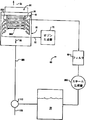
As shown in FIG. 1, a processing system, indicated generally at 10, includes a
[0030]
[0031]
The
[0032]
One or
[0033]
The treatment liquid and ozone are preferably supplied to the
[0034]
The
[0035]
Further, the output of the
[0036]
In the embodiment of the system shown in FIG. 1, the liquid used in the
[0037]
[0038]
The use of high performance ozone generators is particularly useful in combination with the methods and apparatus according to this application. This is because the method and apparatus according to the present invention supply ozone independently of the processing fluid.
[0039]
In a conventional method, ozone is dissolved in an aqueous solution to help the oxidation treatment on the surface of the semiconductor wafer. This limits the amount of ozone supplied to the surface of the semiconductor wafer to the amount of ozone that can be dissolved in the processing fluid. This eliminates the need to use a high performance ozone generator. This is because excessively generated ozone is not absorbed by the process fluid and is ultimately dissipated and lost.
[0040]
FIG. 1 (and other figures as well) shows a preferred design with various components and connections, but this figure includes elements that are essential to the invention as well as elements that are not. The essential elements of the invention are defined in the claims. This figure shows both mandatory and non-essential elements.
[0041]
FIG. 2 shows a further embodiment of a system for supplying a fluid mixture for treating a surface of a semiconductor workpiece. Although the
[0042]
A preferred treatment solution is deionized water. This is because it appears to be necessary to initiate a wash / removal reaction on the workpiece surface, apparently by hydrolysis of the carbon-carbon bonds of the organic molecules. However, significant amounts of water can form a continuous film on the surface of a semiconductor workpiece. This film becomes an obstacle to the diffusion of ozone, thereby suppressing the reaction rate. The thickness of the boundary layer is controlled by the rotational speed of the semiconductor workpiece, the supply of steam, the controlled spray rate of the processing liquid, or a combination of one or more of these techniques. Reducing the thickness of the boundary layer allows the ozone to diffuse to the workpiece surface and react with the organics to be removed.
[0043]
FIG. 3 illustrates one embodiment of a process performed by the system according to FIG. 2 when the
[0044]
In
[0045]
The surface boundary layer of the deionized water is controlled in
[0046]
In
[0047]
The thickness of the surface layer may range from a few molecular layers (eg, about 1 micron) to 100 microns (typically 50-100 microns), and may be greater.
[0048]
Although ozone has only limited solubility in heated deionized water, it can diffuse in water and react with photoresist at the liquid / resist interface. It is believed that the presence of deionized water itself further accelerates the reaction by hydrolyzing carbon-carbon bonds in organic deposits such as photoresist on the wafer surface. Higher temperatures promote dynamic reactions. On the other hand, increasing the concentration of ozone in the gas phase promotes the diffusion of ozone through the boundary layer film. However, raising the temperature of the boundary layer does not actually increase the dissolved ozone concentration.
[0049]
Elevated or higher temperatures mean temperatures above room temperature or room temperature. That is, it means a temperature exceeding 20 to 25 ° C. and up to about 200 ° C.
A preferred temperature range is 25 to 150 ° C, more preferably 55 to 120 ° C or 75 to 115 ° C, and still more preferably 85 to 105 ° C. In the above-mentioned method, a temperature of 90 to 100 ° C. is used, preferably 95 ° C. which is the central temperature.
[0050]
After the
[0051]
In the process described above, the elevated temperature is used to increase the reaction rate at the wafer surface. One approach that will minimize the wafer surface temperature is to maintain a constant supply of a heated processing liquid, such as water or water vapor, during processing. The heated processing liquid contacts and heats the wafer during processing. However, such a constant supply results in considerable waste of water or other processing liquids. To save water and form a boundary layer that is as thin as possible, a “pulse flow” of liquid or steam may be used. If such "pulse flow" is unable to maintain the required elevated wafer surface temperature, an alternative approach that can maintain the wafer surface temperature will be needed. One such alternative is to use a "hot wall" reactor that maintains the temperature of the wafer surface and the processing environment at a desired level. Finally, the processing chamber is heated by, for example, one or more embedded heated recirculation coils, a heating blanket, irradiation by a heat source (eg, an infrared lamp), and the like.
[0052]
In laboratory experiments, 150 mm silicon wafers coated with 1 micron photoresist were stripped according to the process described above. The processing chamber was preheated by spraying deionized water heated to 95 ° C. into the processing chamber for 10 minutes. During the cleaning process, a pulsed flow of deionized water heated to 95 ° C was used. The pulse flow consisted of an "on-time" of approximately 5 seconds followed by an "off-time" of 10 seconds. The wafer was spun at 800 rpm and a pulsed flow of deionized water was sprayed into the processing chamber through nine nozzles at a rate of 3 liters per minute. Ozone was injected into the processing chamber through a separate manifold at a rate of 8 liters per minute at a concentration of 12%. As a result, the peeling speed was 7234 Å / min.
[0053]
At higher ozone flow rates, a high performance ozone generator can be used to inject ozone into the processing chamber to achieve a 19% concentration of ozone at a rate of 12 liters per minute. The speed could be increased to over 8800 Å / min.
[0054]
Using the semiconductor cleaning process described above has many advantages. One of the most important advantages is that a conventional four-step cleaning process can be performed in a two-step chemical process while maintaining the ability to remove organics, remove particles, reduce metals, and remove silicon dioxide. That can be reduced to the process. Processing time, chemical consumption, water usage and waste generation are all significantly reduced. A further advantage of the foregoing process is that it can be applied to FEOL and BEOL wafers and stripping processes. Laboratory tests have shown that metals such as aluminum, titanium, and tungsten are not damaged. A known exception is copper, which forms copper oxide in the presence of ozone. This oxide is not a "hard" uniform passivating oxide, such as an oxide formed on a metal such as aluminum. As a result, the oxide can be easily removed.
[0055]
A further advantage is that higher ozone flow rates and concentrations can be used to achieve higher strip rates under various processing conditions at lower wafer spin rates and lower temperatures. Using a lower temperature between 25 ° C. and 75 ° C., preferably between 25 ° C. and 65 ° C. (as mentioned above, for example, lower than 95 ° C.) may be effective when higher temperatures are not desired. . One example where this is useful is in processing BEOL wafers. In this case, if the metal film is exposed to hot deionized water, corrosion of the metal will occur. The strip speed gain, not seen as a consequence of not using elevated temperatures, can be offset by an increase in strip speed due to the increased ozone flow rate and concentration. The use of higher ozone concentrations can offset the energy loss from using lower temperatures.
[0056]
It will be appreciated that the processing steps 205-215 can be performed substantially simultaneously, as shown again in FIG. It will further be appreciated that processing steps 205-215 may be repeated in sequence using different processing solutions. In such a case, each processing solution used may be specially tailored to remove various combinations of contaminants. However, it is desirable to use as few different processing solutions as possible. By reducing the number of different processing liquids used, the overall cleaning process is simplified, and reducing the number of different processing liquids used minimizes the consumption of chemicals.
[0057]
In a single cycle of processing steps 205-215, a single processing liquid can be used to remove organic contaminants, metals and particles. The processing solution comprises a solution of deionized water and one or more compounds such as HF or HCl to form an acidic processing solution.
[0058]
The use of a hydrofluoric acid solution in processing steps 205-215 has many advantages, including:
[0059]
1. Removal of organic pollutants
The oxidizing power of this process has been repeatedly demonstrated for photoresists. Stripping rates often exceed 8800 Å / min. For cleaning applications, considering the fact that organic contaminants are generally at the molecular level, the process disclosed herein can be said to have sufficient oxidation capacity.
[0060]
2. Oxide removal and controlled chemical oxide regeneration
Depending on the solution temperature and the concentration of HF in the solution, the rate of etching is determined. However, ozone will diffuse through the controlled boundary layer and regenerate oxides to prevent the wafer from becoming hydrophobic. H at 65 ° C 2 A 500: 1 O: HF mixture can be used at a rate of about 6 Å / min. 2 Will be etched. A similar solution at 25.degree. 2 Will be etched. Typical "primary" oxides are generally self-regulated to a thickness of 8 to 12 Angstroms, which is generally the target thickness for oxide removal.
[0061]
3. Particle removal
Although the acidic solution does not have the preferred zeta potential present in the SC1 cleaning described above, the removal of particles in the treatment with the HF treatment solution has the same removal mechanism as etching and regenerating the oxide surface. It was proved that it was used.
[0062]
4. Metal removal
In laboratory experiments, wafers were intentionally contaminated with iron, nickel and copper. It has been proved that the HF treatment including the treatment solution disclosed herein has a reduction in the metal of more than three orders of magnitude. HCl may be used instead of HF as an additive to remove metals. However, the ability to remove oxides and particles is not comparable. The combination of HF and HCl is even more advantageous, each of these agents having great metal removal capacity. However, regenerating the oxide surface by converting the metal to metal oxide and the symbiotic interaction of the two halogen acids creates an exceptionally favorable environment for metal removal.
[0063]
5. An oxide-free (hydrophobic) surface may be formed after removal of the metal, if necessary, by using HF vapor or by using final HF in a dip cell.
[0064]
When HF is used, the uniformity of the thickness of the liquid boundary layer on the wafer or workpiece is important for providing a uniform etch in a direction crossing the wafer. Areas where the boundary layer is thin are etched more slowly and the occurrence of such areas is preferably avoided. Thus, with HF, the rotational speed is preferably reduced to a range of 5-100 rpm, preferably 10-80 rpm or 20-70 rpm, and more preferably 25-50 rpm (typically, for example, 100-400 mm or 200 or 300 mm For workpieces with a diameter or edge dimension of Reducing the rotation speed allows for a thinner boundary layer and more uniform processing. Similar adjustments are preferably made when HF is used or when HCl and HF are used, if other boundary layer controls such as flow rate or spraying are used. HCl or HF may be supplied in a solution injected into the processing liquid, or may be supplied into the room as a dry gas.
[0065]
With HF and ozone, the boundary layer is preferred, and by selecting the flow rate of the liquid on the workpiece surface, the rate of removal of the liquid from the workpiece surface, etc., it is sufficient to ensure good etching uniformity. Maintained in thickness. The liquid boundary layer on the workpiece surface is preferably thick enough to provide an etch uniformity level of less than 5%, preferably less than 3% or 2% (3 sigma division on average). Will be maintained.
[0066]
For processes using HF and ozone, the ozone concentration is preferably about 3-35% or 10-20% by weight (in oxygen). The ozone concentration largely depends on the etching rate of the used HF aqueous solution. When processing silicon, it is desirable that the silicon surface does not transition to a hydrophobic state indicating complete etching of the passive silicon dioxide passivation surface. The HF concentration used is typically 0.001-10% or 0.01-1.0% (by weight). Generally, this concentration is preferably as low as about 0.1% (with a thermal oxide etch rate of 8 Å / min at 95 ° C.) which provides very good cleaning performance. The HF solution may include hydrochloric acid to enhance the ability to remove metals. If this is used, HCl will typically be in a concentration range similar to that described above for HF.
[0067]
In the process using HF and ozone, the temperature range can be set in the range of 0 to 100 ° C. If the process is performed under pressure, higher temperatures may be used. The particle removal capacity of this process is facilitated at elevated temperatures. At room temperature, the particle removal rate of the dried silicon dioxide slurry particles was about 95% when the number of particles initially larger than 0.15 microns was around 60,000. At 65 ° C., this rate was increased to 99%. At 95 ° C., this rate was increased to 99.7%. This may seem like a slight improvement, but is very important in the manufacture of semiconductor devices, as the final particle count is a difference from 3000 to 300 or even 100.
[0068]
Processes using HF and ozone may be used as part of a cleaning procedure. For example, HF / O 3 Is 3:00 (min)> 3:00 SC1> 3:00 HF / O 3 . With this approach, the cleaning efficiency was increased above 99.9%. In contrast, SC1 alone provided only 50% or less washing efficiency. Similar results were obtained when cleaning the silicon nitride particles.
[0069]
The above steps and parameters for the ozone process apply ozone with HF and the ozone process. These processes can be performed on batch workpieces in an apparatus as described in US Pat. No. 5,544,421, or on individual workpieces in an apparatus as described in PCT / US99 / 05676. Can be implemented.
[0070]
Typical chemical treatment times range from 1: 00 to 5:00 minutes. Compared to a four-step cleaning process near 20:00 minutes, the process disclosed herein using HF and / or HCl with processing solution is very attractive. Typical H 2 The concentration ratio of O: HF: HCl is on the order of 500: 1: 1 to 50: 1: 1, with or without HF and / or HCl. It is possible to increase the concentration further, but the economic advantage is reduced. It is important to note that gaseous HF or HCl can be injected into the water to create the desired cleaning agent. Due to the differences between the processor configuration and the desired cleaning requirements, the parameters defined for a particular cleaning process will vary based on these differences and requirements.
[0071]
The advantages of this process are:
1. Reduction of the amount and type of drug used in the cleaning process
2. Reduced water usage by eliminating multiple intermediate rinsing steps required
3. Reduce processing time
4. Simplification of processing hardware
[0072]
The process disclosed here is counterintuitive. Efforts have been made for many years to replace hydrogen peroxide with ozone in chemical treatments such as SC1 and, to a lesser extent, SC2. These efforts usually failed. Because they did not control the boundary layer and did not introduce ozone such that diffusion through the boundary layer was a control mechanism replacing dissolution into this boundary layer. Although the washing efficiency of conventional solutions has been greatly enhanced by increasing the temperature, it has been observed that the solubility of ozone in a given solution is inversely proportional to the temperature of the solution. The solubility of ozone in water at 1 ° C. is approximately 100 ppm. At 60 ° C., this solubility drops to less than 5 ppm. At elevated temperatures, the ozone concentration is thus insufficient to rapidly remove (oxidize) the silicon wafer surface sufficiently to ensure that no pits form on the silicon surface. Thus, these two mechanisms conflict with each other in optimizing the performance of the process.
[0073]
By applying the boundary layer control technique described in connection with the process disclosed herein, a silicon wafer can be processed using a 95: 1 water: ammonium hydroxide 4: 1 solution. Tests have shown empirically that the surface roughness (RMS) is often less than 2 Angstroms. When this same solution is applied to an immersion system or a conventional spraying system, the RMS surface roughness measured by the atomic force microscope increases by more than 20 angstroms and the maximum surface roughness exceeds 190 angstroms. Furthermore, conventional processes have shown that the surface is so porous that it cannot be measured by a light scattering particle counter, but controlled boundary techniques have proven to actually reduce particles by more than 50% at the wafer surface. Was done.
[0074]
When oxidizing and removing organic contaminants, conventional aqueous ozone processes have been demonstrated to have photoresist (hydrocarbon film) stripping rates near 200-700 angstroms per minute. In a boundary layer controlled system according to the process disclosed herein, this rate is increased to 2500-8800 angstroms per minute in the spray controlled boundary layer. Alternatively, it is even higher when the boundary layer is created and controlled using 126 ° C. steam at 15 psi.
[0075]
The process disclosed herein is suitable for widespread use in microelectronic manufacturing applications. One application related to the manufacture of semiconductor devices is reflective notching. To expose a pattern on a semiconductor wafer, the wafer is coated with a photosensitive material called a photoresist. The resistive film is exposed in a light pattern, thereby "exposing" the lighted area. However, since the graphical features are below the photoresist, it is possible for light to pass through the photoresist and reflect the graphical features. This results in exposing the resist in undesirable areas. This reduction is known as "reflective notching". As device densities increase, reflective notching becomes a greater problem.
[0076]
A similar problem arises as a result of reflection perpendicular to the angle of incidence of the light irradiation. Such reflections result in defects in the exposure beam due to the standing wave forming phenomenon, thereby resulting in defects in the photoresist pattern.
[0077]
In order to overcome these phenomena, it has become common to use a non-reflective coating layer. The photoresist film is typically disposed on the upper or lower surface of the non-reflective coating layer. Since the photoresist layer and the anti-reflective coating layer are both only used as "temporary" layers in intermediate manufacturing steps, they must be removed after such intermediate steps are completed.
[0078]
The process shown in FIG. 3 uses a processing solution consisting of water and ammonium hydroxide to remove both the photoresist and the anti-reflective coating in a single processing step (eg, shown in steps 210-215). It has been found that it is acceptable. This has proven to be a concentration between 0.02% and 0.04% by weight with respect to water, but other concentrations are believed to be effective.
[0079]
This process of simultaneously removing the photoresist and the corresponding non-reflective layer is not necessarily limited to processing solutions containing ammonium hydroxide. Rather, the primary goal of the additive is to increase the pH of the solution sprayed on the wafer surface. Preferably, the pH should be raised between about 8.5 and 11. Bases such as sodium hydroxide and / or potassium hydroxide can be used for their removal, but appear less desirable due to mobile ion contamination. However, agents such as TMAH (tetramethylammonium hydroxide) are suitable and do not cause such mobile ion contamination. Ionized water rich in hydroxyl radicals can also be used.
[0080]
The dilute ammonium hydroxide solution can be applied to processes using many techniques. For example, an infusion pump (syringe pump) or other precision drug supply can be used to create a single solution stream. In such an embodiment, it would be possible to strip the photoresist using a stream of deionized water containing ozone, and to strip for a short period while ammonium hydroxide was being injected into the stream of water. Can be. This minimizes drug consumption and waste generation. The dispenser can also monitor and control the pH using suitable sensors and actuators controlled using, for example, a microprocessor.
[0081]
FIG. 4 shows a further embodiment of the
[0082]
FIG. 5 shows a further embodiment of an ozone treatment system, generally designated 250. In the system 250, a
[0083]
FIG. 6 shows a further improvement on any one of the systems described above. In this embodiment, an ultraviolet lamp or an
[0084]
FIG. 7 illustrates a
[0085]
The
[0086]
As described above, the ozone gas may be injected separately or may be introduced into the processing chamber. In this case, it can diffuse through the liquid boundary layer on the workpiece. The fluid is preferably heated and sprayed or otherwise supplied to the workpiece. In this case, no ozone is injected into the fluid before the fluid is supplied to the workpiece.
[0087]
Also, the ozone may be injected into the fluid, and then the ozone may be included in the fluid subsequently supplied to the workpiece. In this embodiment, when the fluid is heated, the heating is preferably performed before the ozone is injected into the fluid, thereby reducing the amount of decomposition of ozone in the fluid during fluid heating. . Typically, due to the large amount of ozone to be injected into the fluid, and due to the low solubility of ozone gas in the heated fluid, the fluid loses some dissolved ozone. As well as ozone bubbles.
[0088]
It is also possible to use the features of both embodiments. That is, it is also possible to introduce ozone gas directly into the processing chamber and to introduce ozone into the fluid before the fluid is supplied into the processing chamber. Thus, various methods can be used to introduce ozone into a room.
[0089]
The apparatus and method disclosed herein can be used to process not only the semiconductor workpieces described above, but also other workpieces. Other workpieces, such as, for example, flat panel displays, hard disk media, CD glass, etc., can also have a treated surface using the apparatus and methods described above.
[0090]
The preferred treatment liquid in the applications disclosed herein is deionized water, but other treatment liquids can also be used. For example, acidic or basic solutions can be used depending on the particular surface to be treated and the material to be removed. Processing solutions containing sulfuric acid, hydrochloric acid and ammonium hydroxide may be useful for various applications.
[0091]
As mentioned above, one feature of this process is the use of steam (water vapor at a temperature above 100 ° C.) to increase the photoresist strip rate in an ozone environment. Preliminary tests have shown that the process using hot water at 95 ° C. has a photoresist strip rate near 3000-4000 Å per minute. A similar process using steam at 120-130 ° C. has resulted in stripping rates near 7000-8000 Å per minute. However, as a result, this stripping speed is not satisfactory.
[0092]
High stripping rates are only realized when steam condenses on the wafer surface. Since the wafer temperature rapidly approaches the thermal equilibrium with steam, when equilibrium is achieved, there is no longer a thermal gradient to promote the formation of a condensate film. This results in loss of the liquid boundary layer on the wafer surface. The boundary layer appears to be essential to promote oxidation of organics on the wafer surface. The absence of a liquid film results in a significant decrease in photoresist strip rate.
[0093]
In addition, once the steam stops condensing on the wafer surface, the reaction environment will lose its energy source for dynamic reactions. As the steam condenses on the wafer surface, approximately 540 calories / gram of heat of evaporation is provided. This energy will then help to facilitate other reactions, such as the oxidation of carbon compounds in the presence of ozone or oxygen-free radicals.
[0094]
In view of these experimental findings, methods for maintaining surface temperatures, such as semiconductor wafer surfaces, have been developed to ensure that condensation from the steam environment continues indefinitely, and that photocondensation in the presence of ozone It will enable steaming in applications such as stripping resist. In this way, the formation of a liquid boundary layer is assured, and a considerable amount of energy release is obtained by the condensation of steam.
[0095]
To achieve this, the wafer surface must be maintained at a temperature lower than the temperature of the steam supplied to the processing chamber. This can be achieved by mounting the wafer on a
[0096]
In a preferred embodiment, a liquid temperature controlled stream is supplied to the backside of the wafer, while steam and ozone are supplied to a closed processing area, and the steam is allowed to condense on the wafer surface. Become. The wafer may be rotated to promote a uniform distribution of the boundary layer and also to assist in defining the thickness of the boundary layer by centrifugal force. However, rotation is not absolutely necessary. The cooling flow must be cooler than steam. If the cooling stream is water, it is preferably at a temperature of 75 or 85-95C and the temperature of the steam is above 100C.
[0097]
In another embodiment, which is relatively easy to implement in a batch process, a pulsed spray of coolant is performed periodically to reduce the wafer temperature. The supply of steam may be continuous or pulsed.
[0098]
The wafer may be in any orientation. And additives such as hydrofluoric acid, ammonium hydroxide or other chemicals may be used to facilitate cleaning of the surface or to remove certain types of substances in place of or in addition to organics. May be added to the system.
[0099]
This process makes it possible to use temperatures higher than 100 ° C. for the purpose of removing organics or other substances from the surface and to promote the reaction in a water / ozone system. It helps to ensure the continuous formation of a condensate film by preventing the surface from being in thermal equilibrium with the steam. It also has the advantage that the heat of evaporation can be used to increase the reaction rate. And a removal process that requires more energy than can be provided by a hydrothermal process can effectively remove more difficult materials.
[Brief description of the drawings]
FIG. 1 is a schematic block diagram of one embodiment of an apparatus for processing semiconductor workpieces, wherein ozone is injected into a pipe containing a pressurized processing liquid.
FIG. 2 is a schematic block diagram of one embodiment of an apparatus for processing a semiconductor workpiece, wherein the semiconductor workpiece heats a processing liquid sprayed onto the surface of the workpiece. Heating indirectly.
FIG. 3 is a flow diagram illustrating one embodiment of a process flow for treating a semiconductor workpiece with a process fluid and ozone.
FIG. 4 is a schematic block diagram of an alternative embodiment to the system shown in FIG. 2, wherein ozone and processing fluid are supplied to the semiconductor workpiece along different flow paths.
FIG. 5 is a schematic block diagram of one embodiment of an apparatus for processing a semiconductor workpiece, wherein pressurized steam and ozone are supplied to a pressurized chamber containing the semiconductor workpiece. Supplied to
FIG. 6 is a schematic block diagram of one embodiment of an apparatus for processing a semiconductor workpiece, wherein an ultraviolet lamp is used to promote a dynamic reaction at the surface of the workpiece. Can be
FIG. 7 is a schematic block diagram of one embodiment of an apparatus for processing a semiconductor workpiece, wherein a gas-liquid contactor is used to promote a dynamic reaction at the surface of the workpiece. Is used.
[Explanation of symbols]
DESCRIPTION OF
Claims (33)
上記ワークピースの表面に加熱された液体を供給するステップであって、上記の加熱された液体が、上記ワークピースを高められた温度に維持するのを助けるようになっているステップと、
上記ワークピースを収容している環境中に、90グラム/時よりも大きい速度でオゾンを導入するステップと、
上記ワークピース上の加熱された液体の厚さを制御して、上記ワークピースの表面での反応のために、オゾンが拡散により通り抜けることができる液体境界層を形成するステップとを含んでいる方法。A method of processing a workpiece, the method comprising:
Providing a heated liquid to a surface of the workpiece, wherein the heated liquid is adapted to help maintain the workpiece at an elevated temperature;
Introducing ozone into the environment containing the workpiece at a rate greater than 90 grams / hour;
Controlling the thickness of the heated liquid on the workpiece to form a liquid boundary layer through which ozone can diffuse through for reaction at the surface of the workpiece. .
上記ワークピースの表面に水と、HFまたはHClとからなる加熱された溶液を供給するステップであって、上記の加熱された溶液は、上記ワークピースを高められた温度に維持するのを助けるようになっているステップと、
上記ワークピースを収容している環境中に、90グラム/時よりも大きい速度でオゾンを導入するステップと、
上記の加熱された溶液の厚さを制御して、上記ワークピースの表面に液体境界層を形成し、上記ワークピースの表面での反応のために、オゾンが上記境界層を通って拡散するのを可能にするステップとを含んでいる方法。A method for cleaning a surface of a workpiece, the method comprising:
Providing a heated solution of water and HF or HCl to the surface of the workpiece, wherein the heated solution helps maintain the workpiece at an elevated temperature. Steps with
Introducing ozone into the environment containing the workpiece at a rate greater than 90 grams / hour;
The thickness of the heated solution is controlled to form a liquid boundary layer on the surface of the workpiece, and ozone diffuses through the boundary layer for reaction at the surface of the workpiece. And the step of enabling.
液体室を有する液体容器と、
上記ワークピースに流体を供給するための、処理室内の1つまたは複数のノズルと、
上記液体室をノズルに接続する流体通路と、
90gpmより大きい容量を有し、上記流体通路内または室内にオゾンを注入するためのオゾン供給システムと、
上記液体をワークピースに供給する前に、上記液体を加熱する加熱器とを含んでいるシステム。A system for processing a workpiece, the system comprising:
A liquid container having a liquid chamber;
One or more nozzles in a processing chamber for supplying fluid to the workpiece;
A fluid passage connecting the liquid chamber to a nozzle,
An ozone supply system having a capacity greater than 90 gpm for injecting ozone into the fluid passage or chamber;
A heater for heating the liquid before supplying the liquid to the workpiece.
上記ワークピースを回転させるロータと、
上記液体の流速を制御する流量コントローラと、
上記処理液の微細な液滴を生成するようになっている1つまたは複数のノズルのうちの少なくとも1つを備えている、請求項19に記載のシステム。Further comprising means for controlling the thickness of the liquid layer on the workpiece,
A rotor for rotating the workpiece,
A flow controller for controlling the flow rate of the liquid,
20. The system of claim 19, comprising at least one of one or more nozzles adapted to generate fine droplets of the processing liquid.
上記ワークピースの表面に液体を導入するステップと、
上記ワークピースの周囲環境に90グラム/時より大きい速度でオゾンを導入するステップと、
上記ワークピースの表面上の液体の厚さを制御して、上記ワークピースの表面上の液体を通ってオゾンが拡散するのを可能にするステップとを含んでいる方法。A method of processing a workpiece, the method comprising:
Introducing a liquid to the surface of the workpiece;
Introducing ozone into the environment surrounding the workpiece at a rate greater than 90 grams / hour;
Controlling the thickness of the liquid on the surface of the workpiece to allow ozone to diffuse through the liquid on the surface of the workpiece.
上記ワークピースの表面に、HFを含む液体を導入するステップと、
上記ワークピースの表面上の液体を通してオゾンを拡散させるステップと、
上記ワークピースの表面上の液体層の厚さを制御して、実質的に均一なエッチングを行なわせるステップとを含んでいる方法。A method of processing a workpiece, the method comprising:
Introducing a liquid containing HF to the surface of the workpiece;
Diffusing ozone through a liquid on the surface of the workpiece;
Controlling the thickness of the liquid layer on the surface of the workpiece to effect a substantially uniform etch.
Applications Claiming Priority (2)
| Application Number | Priority Date | Filing Date | Title |
|---|---|---|---|
| US14535099P | 1999-07-23 | 1999-07-23 | |
| PCT/US2000/020036 WO2001007177A1 (en) | 1999-07-23 | 2000-07-21 | Process and apparatus for treating a workpiece such as a semiconductor wafer |
Related Child Applications (2)
| Application Number | Title | Priority Date | Filing Date |
|---|---|---|---|
| JP2006119518A Division JP2006261685A (en) | 1999-07-23 | 2006-04-24 | Process and apparatus for treating workpiece such as semiconductor wafer |
| JP2006254509A Division JP2007049176A (en) | 1999-07-23 | 2006-09-20 | Method and device for processing workpiece such as semiconductor wafer |
Publications (2)
| Publication Number | Publication Date |
|---|---|
| JP2004500701A true JP2004500701A (en) | 2004-01-08 |
| JP2004500701A5 JP2004500701A5 (en) | 2005-12-22 |
Family
ID=22512696
Family Applications (3)
| Application Number | Title | Priority Date | Filing Date |
|---|---|---|---|
| JP2001512043A Pending JP2004500701A (en) | 1999-07-23 | 2000-07-21 | Method and apparatus for processing a workpiece such as a semiconductor wafer |
| JP2006119518A Pending JP2006261685A (en) | 1999-07-23 | 2006-04-24 | Process and apparatus for treating workpiece such as semiconductor wafer |
| JP2006254509A Pending JP2007049176A (en) | 1999-07-23 | 2006-09-20 | Method and device for processing workpiece such as semiconductor wafer |
Family Applications After (2)
| Application Number | Title | Priority Date | Filing Date |
|---|---|---|---|
| JP2006119518A Pending JP2006261685A (en) | 1999-07-23 | 2006-04-24 | Process and apparatus for treating workpiece such as semiconductor wafer |
| JP2006254509A Pending JP2007049176A (en) | 1999-07-23 | 2006-09-20 | Method and device for processing workpiece such as semiconductor wafer |
Country Status (6)
| Country | Link |
|---|---|
| EP (2) | EP1212151A4 (en) |
| JP (3) | JP2004500701A (en) |
| AT (1) | ATE485115T1 (en) |
| DE (1) | DE60045134D1 (en) |
| TW (1) | TW472317B (en) |
| WO (1) | WO2001007177A1 (en) |
Cited By (3)
| Publication number | Priority date | Publication date | Assignee | Title |
|---|---|---|---|---|
| JP2006093473A (en) * | 2004-09-24 | 2006-04-06 | M Fsi Kk | Method and apparatus for cleaning substrate |
| JP2007236706A (en) * | 2006-03-09 | 2007-09-20 | Hiroshima Univ | Washing apparatus for washing object to be washed of food manufacturing facility, and washing method |
| JP2012134199A (en) * | 2010-12-20 | 2012-07-12 | Tokyo Electron Ltd | Slimming method of thin film containing carbon and oxidation device |
Families Citing this family (16)
| Publication number | Priority date | Publication date | Assignee | Title |
|---|---|---|---|---|
| JP4917651B2 (en) * | 1999-08-12 | 2012-04-18 | アクアサイエンス株式会社 | Resist film removing apparatus and resist film removing method |
| US6982006B1 (en) | 1999-10-19 | 2006-01-03 | Boyers David G | Method and apparatus for treating a substrate with an ozone-solvent solution |
| JP4000247B2 (en) * | 2001-04-18 | 2007-10-31 | 株式会社ルネサステクノロジ | Photomask cleaning method |
| EP1347496A3 (en) | 2002-03-12 | 2006-05-03 | Dainippon Screen Mfg. Co., Ltd. | Substrate treating apparatus and substrate treating method |
| JP4232383B2 (en) * | 2002-05-13 | 2009-03-04 | 信越半導体株式会社 | Method for surface treatment of semiconductor wafer |
| KR100467016B1 (en) * | 2002-05-30 | 2005-01-24 | 삼성전자주식회사 | Method of cleaning semiconductor substrate |
| DE102007027112B4 (en) * | 2007-06-13 | 2011-06-22 | Siltronic AG, 81737 | Process for cleaning, drying and hydrophilizing a semiconductor wafer |
| JP2008311591A (en) * | 2007-06-18 | 2008-12-25 | Sharp Corp | Substrate treatment method and substrate treatment equipment |
| US7955440B2 (en) * | 2007-12-07 | 2011-06-07 | Sumco Corporation | Method for cleaning silicon wafer and apparatus for cleaning the silicon wafer |
| CA2715680C (en) * | 2008-02-21 | 2016-05-17 | Unilever Plc | A process and a device to clean substrates |
| IT1395090B1 (en) * | 2009-04-08 | 2012-09-05 | Lasa Impianti Srl | LOW ENVIRONMENTAL IMPACT EQUIPMENT FOR WASHING METAL AND NON-METALLIC DETAILS THAT NEED ANOTHER DEGREE OF CLEANING |
| JP5520991B2 (en) * | 2012-03-29 | 2014-06-11 | 芝浦メカトロニクス株式会社 | Substrate processing apparatus and processing method |
| WO2013158937A1 (en) * | 2012-04-18 | 2013-10-24 | Advanced Wet Technologies Gmbh | Hyperbaric methods and systems for rinsing and drying granular materials |
| US11358172B2 (en) * | 2015-09-24 | 2022-06-14 | Suss Microtec Photomask Equipment Gmbh & Co. Kg | Method for treating substrates with an aqueous liquid medium exposed to UV-radiation |
| WO2018076187A1 (en) * | 2016-10-25 | 2018-05-03 | 深圳市柔宇科技有限公司 | Liquid temperature control system and film layer peeling device |
| JP7353212B2 (en) | 2020-02-28 | 2023-09-29 | 株式会社Screenホールディングス | Substrate processing equipment |
Family Cites Families (12)
| Publication number | Priority date | Publication date | Assignee | Title |
|---|---|---|---|---|
| US5232511A (en) * | 1990-05-15 | 1993-08-03 | Semitool, Inc. | Dynamic semiconductor wafer processing using homogeneous mixed acid vapors |
| US5261966A (en) * | 1991-01-28 | 1993-11-16 | Kabushiki Kaisha Toshiba | Method of cleaning semiconductor wafers using mixer containing a bundle of gas permeable hollow yarns |
| JPH05152203A (en) * | 1991-11-29 | 1993-06-18 | Chlorine Eng Corp Ltd | Method and device for treating substrate |
| KR940012061A (en) * | 1992-11-27 | 1994-06-22 | 가나이 쯔또무 | Organic matter removal method and organic matter removal apparatus for using the method |
| US5464480A (en) * | 1993-07-16 | 1995-11-07 | Legacy Systems, Inc. | Process and apparatus for the treatment of semiconductor wafers in a fluid |
| JP2760418B2 (en) * | 1994-07-29 | 1998-05-28 | 住友シチックス株式会社 | Semiconductor wafer cleaning solution and method for cleaning semiconductor wafer using the same |
| JP3923097B2 (en) * | 1995-03-06 | 2007-05-30 | 忠弘 大見 | Cleaning device |
| JPH0969509A (en) * | 1995-09-01 | 1997-03-11 | Matsushita Electron Corp | Cleaning/etching/drying system for semiconductor wafer and using method thereof |
| US5803982A (en) * | 1996-10-15 | 1998-09-08 | Ez Environmental Solutions Corporation | Pressure washing apparatus with ozone generator |
| ATE522926T1 (en) * | 1997-02-14 | 2011-09-15 | Imec | METHOD FOR REMOVAL OF ORGANIC CONTAMINATION FROM A SEMICONDUCTOR SURFACE |
| JPH10340876A (en) * | 1997-06-10 | 1998-12-22 | Shibaura Eng Works Co Ltd | Cleaning treatment method and cleaning treatment equipment |
| JP4477704B2 (en) * | 1997-11-20 | 2010-06-09 | アイメック | Method for removing organic contaminants from semiconductor substrate surface |
-
2000
- 2000-07-21 WO PCT/US2000/020036 patent/WO2001007177A1/en active Application Filing
- 2000-07-21 EP EP00948892A patent/EP1212151A4/en not_active Withdrawn
- 2000-07-21 AT AT04020205T patent/ATE485115T1/en active
- 2000-07-21 EP EP04020205A patent/EP1481741B1/en not_active Expired - Lifetime
- 2000-07-21 DE DE60045134T patent/DE60045134D1/en not_active Expired - Lifetime
- 2000-07-21 JP JP2001512043A patent/JP2004500701A/en active Pending
- 2000-07-21 TW TW089114615A patent/TW472317B/en not_active IP Right Cessation
-
2006
- 2006-04-24 JP JP2006119518A patent/JP2006261685A/en active Pending
- 2006-09-20 JP JP2006254509A patent/JP2007049176A/en active Pending
Cited By (3)
| Publication number | Priority date | Publication date | Assignee | Title |
|---|---|---|---|---|
| JP2006093473A (en) * | 2004-09-24 | 2006-04-06 | M Fsi Kk | Method and apparatus for cleaning substrate |
| JP2007236706A (en) * | 2006-03-09 | 2007-09-20 | Hiroshima Univ | Washing apparatus for washing object to be washed of food manufacturing facility, and washing method |
| JP2012134199A (en) * | 2010-12-20 | 2012-07-12 | Tokyo Electron Ltd | Slimming method of thin film containing carbon and oxidation device |
Also Published As
| Publication number | Publication date |
|---|---|
| TW472317B (en) | 2002-01-11 |
| JP2007049176A (en) | 2007-02-22 |
| EP1212151A1 (en) | 2002-06-12 |
| EP1481741B1 (en) | 2010-10-20 |
| ATE485115T1 (en) | 2010-11-15 |
| JP2006261685A (en) | 2006-09-28 |
| WO2001007177A1 (en) | 2001-02-01 |
| EP1481741A3 (en) | 2005-08-17 |
| DE60045134D1 (en) | 2010-12-02 |
| EP1212151A4 (en) | 2005-08-17 |
| EP1481741A2 (en) | 2004-12-01 |
Similar Documents
| Publication | Publication Date | Title |
|---|---|---|
| US6837252B2 (en) | Apparatus for treating a workpiece with steam and ozone | |
| JP2007049176A (en) | Method and device for processing workpiece such as semiconductor wafer | |
| KR100572295B1 (en) | Process and apparatus for treating a workpiece such as a semiconductor wafer | |
| US6582525B2 (en) | Methods for processing a workpiece using steam and ozone | |
| JP3977807B2 (en) | Processing and equipment for handling workpieces such as semiconductor wafers | |
| JP2004538635A5 (en) | ||
| US7264680B2 (en) | Process and apparatus for treating a workpiece using ozone | |
| US7163588B2 (en) | Processing a workpiece using water, a base, and ozone | |
| US20060151007A1 (en) | Workpiece processing using ozone gas and chelating agents | |
| KR20080071988A (en) | Process for removing material from substrates | |
| US20050034745A1 (en) | Processing a workpiece with ozone and a halogenated additive |
Legal Events
| Date | Code | Title | Description |
|---|---|---|---|
| A521 | Request for written amendment filed |
Free format text: JAPANESE INTERMEDIATE CODE: A523 Effective date: 20040705 |
|
| A621 | Written request for application examination |
Free format text: JAPANESE INTERMEDIATE CODE: A621 Effective date: 20040705 |
|
| A977 | Report on retrieval |
Free format text: JAPANESE INTERMEDIATE CODE: A971007 Effective date: 20051122 |
|
| A131 | Notification of reasons for refusal |
Free format text: JAPANESE INTERMEDIATE CODE: A131 Effective date: 20060124 |
|
| A521 | Request for written amendment filed |
Free format text: JAPANESE INTERMEDIATE CODE: A523 Effective date: 20060424 |
|
| A02 | Decision of refusal |
Free format text: JAPANESE INTERMEDIATE CODE: A02 Effective date: 20060523 |
|
| A601 | Written request for extension of time |
Free format text: JAPANESE INTERMEDIATE CODE: A601 Effective date: 20081104 |
|
| A602 | Written permission of extension of time |
Free format text: JAPANESE INTERMEDIATE CODE: A602 Effective date: 20081107 |
|
| A601 | Written request for extension of time |
Free format text: JAPANESE INTERMEDIATE CODE: A601 Effective date: 20081205 |
|
| A602 | Written permission of extension of time |
Free format text: JAPANESE INTERMEDIATE CODE: A602 Effective date: 20081210 |
|
| A601 | Written request for extension of time |
Free format text: JAPANESE INTERMEDIATE CODE: A601 Effective date: 20081226 |
|
| A602 | Written permission of extension of time |
Free format text: JAPANESE INTERMEDIATE CODE: A602 Effective date: 20090107 |