JP2004335641A - Method of manufacturing substrate having built-in semiconductor element - Google Patents
Method of manufacturing substrate having built-in semiconductor element Download PDFInfo
- Publication number
- JP2004335641A JP2004335641A JP2003127990A JP2003127990A JP2004335641A JP 2004335641 A JP2004335641 A JP 2004335641A JP 2003127990 A JP2003127990 A JP 2003127990A JP 2003127990 A JP2003127990 A JP 2003127990A JP 2004335641 A JP2004335641 A JP 2004335641A
- Authority
- JP
- Japan
- Prior art keywords
- semiconductor element
- sheet
- semiconductor chip
- substrate
- manufacturing
- Prior art date
- Legal status (The legal status is an assumption and is not a legal conclusion. Google has not performed a legal analysis and makes no representation as to the accuracy of the status listed.)
- Withdrawn
Links
Images


Classifications
-
- H—ELECTRICITY
- H01—ELECTRIC ELEMENTS
- H01L—SEMICONDUCTOR DEVICES NOT COVERED BY CLASS H10
- H01L24/00—Arrangements for connecting or disconnecting semiconductor or solid-state bodies; Methods or apparatus related thereto
- H01L24/01—Means for bonding being attached to, or being formed on, the surface to be connected, e.g. chip-to-package, die-attach, "first-level" interconnects; Manufacturing methods related thereto
- H01L24/18—High density interconnect [HDI] connectors; Manufacturing methods related thereto
- H01L24/19—Manufacturing methods of high density interconnect preforms
-
- H—ELECTRICITY
- H01—ELECTRIC ELEMENTS
- H01L—SEMICONDUCTOR DEVICES NOT COVERED BY CLASS H10
- H01L2224/00—Indexing scheme for arrangements for connecting or disconnecting semiconductor or solid-state bodies and methods related thereto as covered by H01L24/00
- H01L2224/01—Means for bonding being attached to, or being formed on, the surface to be connected, e.g. chip-to-package, die-attach, "first-level" interconnects; Manufacturing methods related thereto
- H01L2224/02—Bonding areas; Manufacturing methods related thereto
- H01L2224/04—Structure, shape, material or disposition of the bonding areas prior to the connecting process
- H01L2224/0401—Bonding areas specifically adapted for bump connectors, e.g. under bump metallisation [UBM]
-
- H—ELECTRICITY
- H01—ELECTRIC ELEMENTS
- H01L—SEMICONDUCTOR DEVICES NOT COVERED BY CLASS H10
- H01L2224/00—Indexing scheme for arrangements for connecting or disconnecting semiconductor or solid-state bodies and methods related thereto as covered by H01L24/00
- H01L2224/01—Means for bonding being attached to, or being formed on, the surface to be connected, e.g. chip-to-package, die-attach, "first-level" interconnects; Manufacturing methods related thereto
- H01L2224/02—Bonding areas; Manufacturing methods related thereto
- H01L2224/04—Structure, shape, material or disposition of the bonding areas prior to the connecting process
- H01L2224/04105—Bonding areas formed on an encapsulation of the semiconductor or solid-state body, e.g. bonding areas on chip-scale packages
-
- H—ELECTRICITY
- H01—ELECTRIC ELEMENTS
- H01L—SEMICONDUCTOR DEVICES NOT COVERED BY CLASS H10
- H01L2224/00—Indexing scheme for arrangements for connecting or disconnecting semiconductor or solid-state bodies and methods related thereto as covered by H01L24/00
- H01L2224/01—Means for bonding being attached to, or being formed on, the surface to be connected, e.g. chip-to-package, die-attach, "first-level" interconnects; Manufacturing methods related thereto
- H01L2224/10—Bump connectors; Manufacturing methods related thereto
- H01L2224/12—Structure, shape, material or disposition of the bump connectors prior to the connecting process
- H01L2224/12105—Bump connectors formed on an encapsulation of the semiconductor or solid-state body, e.g. bumps on chip-scale packages
-
- H—ELECTRICITY
- H01—ELECTRIC ELEMENTS
- H01L—SEMICONDUCTOR DEVICES NOT COVERED BY CLASS H10
- H01L2224/00—Indexing scheme for arrangements for connecting or disconnecting semiconductor or solid-state bodies and methods related thereto as covered by H01L24/00
- H01L2224/01—Means for bonding being attached to, or being formed on, the surface to be connected, e.g. chip-to-package, die-attach, "first-level" interconnects; Manufacturing methods related thereto
- H01L2224/18—High density interconnect [HDI] connectors; Manufacturing methods related thereto
- H01L2224/19—Manufacturing methods of high density interconnect preforms
-
- H—ELECTRICITY
- H01—ELECTRIC ELEMENTS
- H01L—SEMICONDUCTOR DEVICES NOT COVERED BY CLASS H10
- H01L2224/00—Indexing scheme for arrangements for connecting or disconnecting semiconductor or solid-state bodies and methods related thereto as covered by H01L24/00
- H01L2224/01—Means for bonding being attached to, or being formed on, the surface to be connected, e.g. chip-to-package, die-attach, "first-level" interconnects; Manufacturing methods related thereto
- H01L2224/26—Layer connectors, e.g. plate connectors, solder or adhesive layers; Manufacturing methods related thereto
- H01L2224/31—Structure, shape, material or disposition of the layer connectors after the connecting process
- H01L2224/32—Structure, shape, material or disposition of the layer connectors after the connecting process of an individual layer connector
- H01L2224/321—Disposition
- H01L2224/32135—Disposition the layer connector connecting between different semiconductor or solid-state bodies, i.e. chip-to-chip
- H01L2224/32145—Disposition the layer connector connecting between different semiconductor or solid-state bodies, i.e. chip-to-chip the bodies being stacked
-
- H—ELECTRICITY
- H01—ELECTRIC ELEMENTS
- H01L—SEMICONDUCTOR DEVICES NOT COVERED BY CLASS H10
- H01L2224/00—Indexing scheme for arrangements for connecting or disconnecting semiconductor or solid-state bodies and methods related thereto as covered by H01L24/00
- H01L2224/01—Means for bonding being attached to, or being formed on, the surface to be connected, e.g. chip-to-package, die-attach, "first-level" interconnects; Manufacturing methods related thereto
- H01L2224/26—Layer connectors, e.g. plate connectors, solder or adhesive layers; Manufacturing methods related thereto
- H01L2224/31—Structure, shape, material or disposition of the layer connectors after the connecting process
- H01L2224/32—Structure, shape, material or disposition of the layer connectors after the connecting process of an individual layer connector
- H01L2224/321—Disposition
- H01L2224/32151—Disposition the layer connector connecting between a semiconductor or solid-state body and an item not being a semiconductor or solid-state body, e.g. chip-to-substrate, chip-to-passive
- H01L2224/32221—Disposition the layer connector connecting between a semiconductor or solid-state body and an item not being a semiconductor or solid-state body, e.g. chip-to-substrate, chip-to-passive the body and the item being stacked
- H01L2224/32225—Disposition the layer connector connecting between a semiconductor or solid-state body and an item not being a semiconductor or solid-state body, e.g. chip-to-substrate, chip-to-passive the body and the item being stacked the item being non-metallic, e.g. insulating substrate with or without metallisation
-
- H—ELECTRICITY
- H01—ELECTRIC ELEMENTS
- H01L—SEMICONDUCTOR DEVICES NOT COVERED BY CLASS H10
- H01L2224/00—Indexing scheme for arrangements for connecting or disconnecting semiconductor or solid-state bodies and methods related thereto as covered by H01L24/00
- H01L2224/01—Means for bonding being attached to, or being formed on, the surface to be connected, e.g. chip-to-package, die-attach, "first-level" interconnects; Manufacturing methods related thereto
- H01L2224/42—Wire connectors; Manufacturing methods related thereto
- H01L2224/47—Structure, shape, material or disposition of the wire connectors after the connecting process
- H01L2224/48—Structure, shape, material or disposition of the wire connectors after the connecting process of an individual wire connector
- H01L2224/481—Disposition
- H01L2224/48151—Connecting between a semiconductor or solid-state body and an item not being a semiconductor or solid-state body, e.g. chip-to-substrate, chip-to-passive
- H01L2224/48221—Connecting between a semiconductor or solid-state body and an item not being a semiconductor or solid-state body, e.g. chip-to-substrate, chip-to-passive the body and the item being stacked
- H01L2224/48225—Connecting between a semiconductor or solid-state body and an item not being a semiconductor or solid-state body, e.g. chip-to-substrate, chip-to-passive the body and the item being stacked the item being non-metallic, e.g. insulating substrate with or without metallisation
- H01L2224/48227—Connecting between a semiconductor or solid-state body and an item not being a semiconductor or solid-state body, e.g. chip-to-substrate, chip-to-passive the body and the item being stacked the item being non-metallic, e.g. insulating substrate with or without metallisation connecting the wire to a bond pad of the item
-
- H—ELECTRICITY
- H01—ELECTRIC ELEMENTS
- H01L—SEMICONDUCTOR DEVICES NOT COVERED BY CLASS H10
- H01L2224/00—Indexing scheme for arrangements for connecting or disconnecting semiconductor or solid-state bodies and methods related thereto as covered by H01L24/00
- H01L2224/73—Means for bonding being of different types provided for in two or more of groups H01L2224/10, H01L2224/18, H01L2224/26, H01L2224/34, H01L2224/42, H01L2224/50, H01L2224/63, H01L2224/71
- H01L2224/732—Location after the connecting process
- H01L2224/73251—Location after the connecting process on different surfaces
- H01L2224/73265—Layer and wire connectors
-
- H—ELECTRICITY
- H01—ELECTRIC ELEMENTS
- H01L—SEMICONDUCTOR DEVICES NOT COVERED BY CLASS H10
- H01L2224/00—Indexing scheme for arrangements for connecting or disconnecting semiconductor or solid-state bodies and methods related thereto as covered by H01L24/00
- H01L2224/73—Means for bonding being of different types provided for in two or more of groups H01L2224/10, H01L2224/18, H01L2224/26, H01L2224/34, H01L2224/42, H01L2224/50, H01L2224/63, H01L2224/71
- H01L2224/732—Location after the connecting process
- H01L2224/73251—Location after the connecting process on different surfaces
- H01L2224/73267—Layer and HDI connectors
-
- H—ELECTRICITY
- H01—ELECTRIC ELEMENTS
- H01L—SEMICONDUCTOR DEVICES NOT COVERED BY CLASS H10
- H01L2225/00—Details relating to assemblies covered by the group H01L25/00 but not provided for in its subgroups
- H01L2225/03—All the devices being of a type provided for in the same subgroup of groups H01L27/00 - H01L33/648 and H10K99/00
- H01L2225/10—All the devices being of a type provided for in the same subgroup of groups H01L27/00 - H01L33/648 and H10K99/00 the devices having separate containers
- H01L2225/1005—All the devices being of a type provided for in the same subgroup of groups H01L27/00 - H01L33/648 and H10K99/00 the devices having separate containers the devices being of a type provided for in group H01L27/00
- H01L2225/1011—All the devices being of a type provided for in the same subgroup of groups H01L27/00 - H01L33/648 and H10K99/00 the devices having separate containers the devices being of a type provided for in group H01L27/00 the containers being in a stacked arrangement
- H01L2225/1017—All the devices being of a type provided for in the same subgroup of groups H01L27/00 - H01L33/648 and H10K99/00 the devices having separate containers the devices being of a type provided for in group H01L27/00 the containers being in a stacked arrangement the lowermost container comprising a device support
- H01L2225/1035—All the devices being of a type provided for in the same subgroup of groups H01L27/00 - H01L33/648 and H10K99/00 the devices having separate containers the devices being of a type provided for in group H01L27/00 the containers being in a stacked arrangement the lowermost container comprising a device support the device being entirely enclosed by the support, e.g. high-density interconnect [HDI]
-
- H—ELECTRICITY
- H01—ELECTRIC ELEMENTS
- H01L—SEMICONDUCTOR DEVICES NOT COVERED BY CLASS H10
- H01L24/00—Arrangements for connecting or disconnecting semiconductor or solid-state bodies; Methods or apparatus related thereto
- H01L24/73—Means for bonding being of different types provided for in two or more of groups H01L24/10, H01L24/18, H01L24/26, H01L24/34, H01L24/42, H01L24/50, H01L24/63, H01L24/71
-
- H—ELECTRICITY
- H01—ELECTRIC ELEMENTS
- H01L—SEMICONDUCTOR DEVICES NOT COVERED BY CLASS H10
- H01L2924/00—Indexing scheme for arrangements or methods for connecting or disconnecting semiconductor or solid-state bodies as covered by H01L24/00
- H01L2924/06—Polymers
- H01L2924/078—Adhesive characteristics other than chemical
- H01L2924/07802—Adhesive characteristics other than chemical not being an ohmic electrical conductor
-
- H—ELECTRICITY
- H01—ELECTRIC ELEMENTS
- H01L—SEMICONDUCTOR DEVICES NOT COVERED BY CLASS H10
- H01L2924/00—Indexing scheme for arrangements or methods for connecting or disconnecting semiconductor or solid-state bodies as covered by H01L24/00
- H01L2924/15—Details of package parts other than the semiconductor or other solid state devices to be connected
- H01L2924/151—Die mounting substrate
- H01L2924/153—Connection portion
- H01L2924/1531—Connection portion the connection portion being formed only on the surface of the substrate opposite to the die mounting surface
- H01L2924/15311—Connection portion the connection portion being formed only on the surface of the substrate opposite to the die mounting surface being a ball array, e.g. BGA
-
- H—ELECTRICITY
- H01—ELECTRIC ELEMENTS
- H01L—SEMICONDUCTOR DEVICES NOT COVERED BY CLASS H10
- H01L2924/00—Indexing scheme for arrangements or methods for connecting or disconnecting semiconductor or solid-state bodies as covered by H01L24/00
- H01L2924/30—Technical effects
- H01L2924/35—Mechanical effects
- H01L2924/351—Thermal stress
Landscapes
- Engineering & Computer Science (AREA)
- Manufacturing & Machinery (AREA)
- Computer Hardware Design (AREA)
- Microelectronics & Electronic Packaging (AREA)
- Power Engineering (AREA)
- Production Of Multi-Layered Print Wiring Board (AREA)
Abstract
Description
【0001】
【発明の属する技術分野】
本発明は、回路基板に電気回路部品を実装した半導体素子内蔵基板の製造方法に関するものである。
【0002】
【従来の技術】
近年電子機器製品の小型・軽量化のため、電子機器製品内に組み込まれる半導体素子内蔵基板の小型化が望まれている。
【0003】
従来の半導体素子内蔵基板の小型化の手段として、プリプレグからなり孔部を有する枠材を底板にプレス積層して凹部を有する基板を形成し、その後に半導体チップを凹部に貼り付けた後圧着し、さらにその上に絶縁層や配線層を形成し、さらにその上に電気回路部品を実装する方法が提案されている(例えば特許文献1参照。)
また、半導体チップを回路基板上に逐次積層していく方法が提案されている。(例えば特許文献2参照。)
さらには、半導体チップの電極部にバンプを形成して絶縁樹脂を塗布して埋め込み、研磨する方法が提案されている。(例えば特許文献3参照。)
【特許文献1】
特開2002−16173号公報(第4頁)
【特許文献2】
特開平5−13967号公報
【特許文献3】
特開2002−290006号公報
【0004】
【発明が解決しようとする課題】
しかしながら、特開2002−16173号公報記載の発明には次のような課題があった。
【0005】
基板を積層する際のプレス工程においてプレス圧力が不均一となり密着不足を発生させたり、凹部の形状が不均一になる。特に、熱プレスを用いた場合、プリプレグ中の樹脂が熱プレス工程により軟化して凹部内に流れ込み、凹部の底に大きな凹凸をもったり、最悪の場合凹部が埋まってしまい、後に半導体チップを載置するために必要な凹部形状が保てない。
【0006】
また、半導体チップを埋め込むためには、回路基板凹部の底に半導体チップを保持できるようにするための保持面を形成しなければならず、この保持面のための絶縁層が必要になるが、このようにすると半導体チップを挟んだ導体層間の絶縁層の厚みは、半導体チップ厚に保持面上の絶縁層の厚みが加わったものとなり非常に厚くなってしまう。そのため、複数の層からなる回路基板の複数の層間に半導体チップを埋め込んだ場合、回路基板の層厚がきわめて厚くなり小型化できなくなる。
【0007】
さらに、このように凹部を形成した後に半導体チップを組み込み、その後に埋め込む方式では、多層化していく際に各々の層毎に凹部を形成していかなければならず、極めて生産効率が悪い。
【0008】
また、このような凹部を基板に設けその中に半導体チップを搭載し、その後にこの半導体チップを覆うために液状絶縁性樹脂を用いる方法では、絶縁樹脂の硬化収縮時の樹脂量が面内で異なることから、硬化後の絶縁性樹脂表面の均一性・平坦性が得られ難く、そのため、露光・現像・エッチング工程にてレジスト像が乱れ、微細な配線パターンの形成をおこなうことができない。特に半導体チップ周辺は、チップ厚み分の樹脂が硬化収縮するため、表面が凹になりやすい。
【0009】
凹部を形成しないで埋め込む方式の場合には、基板の表面にあらかじめ形成された配線パターンの電極部と半導体チップの電極部とを接続する接合工程が必ず必要になる。
【0010】
この接続を行う方法として、フリップチップ接続をおこなう場合には、半導体チップの電極パッド部にはんだバンプあるいはボールを形成させる必要がある。
そして、この半導体チップのはんだバンプと基板の配線パターンの電極部とを位置合わせの後に半導体チップをパターン電極上に搭載し、加熱することで接合させる。そして、半導体チップ表面と基板表面との間のバンプによってできているギャップ間にアンダーフィル材と呼ばれる接続補強樹脂を注入し固着させるといた複雑な接合工程が必要となる。
【0011】
さらに、このようなフリップチップ接続を今後の多ピン化が進む半導体チップで行おうとするならば、半導体チップに形成されるバンプやハンダボールの微細化かつ高精度化が要求されるだけでなく、基板の配線ピッチも、より微細化を要求される。そのため、バンプ形成コストと基板コストが大幅に上昇する。さらに、搭載時の位置合わせ精度もより厳しいものが要求され、装置コストの上昇を招いてしまう。
【0012】
逐次積層していく方式では、常に半導体チップの電極部は、同一面方向を向かざるを得ない。そのため、半導体チップと半導体チップとの間を接続するには、最短でも半導体Chip厚以上は必要になり配線長を短くすることが難しい。そのため、より高速な信号の伝送を行う際に信号波形の遅れや波形形状の乱れになり、高速な信号伝送が難しい。
【0013】
また、半導体チップ上に積層されかつ、各半導体チップの電極部より配線を接続するためには、必ず半導体チップ上に積層される半導体チップのサイズは、その下の半導体チップより小さくなくてはならず、積層する各半導体チップがそのサイズによって限定されるといった設計制約がある。
【0014】
半導体チップの電極部にバンプを形成して絶縁樹脂を塗布して埋め込み、研磨する方式では、バンプ上を覆っている絶縁樹脂を除去するためと、絶縁樹脂表面を平坦化させるために必ず研磨工程が必要になる。一方レーザーによってスタッドバンプを露出させるものに関しては、反射率の高い金からなり、かつネックカットした形状安定性の悪いスタッドバンプにレーザー光があたると、レーザー光が反射・散乱され加工穴形状が著しく悪くなる。そのため、通常100μm以下という極めて狭ピッチな半導体チップの電極部ピッチに対して、安定した接続用の穴加工を行うことができない。
【0015】
また、穴加工精度を緩和させるための半導体チップ電極面積より大きいバンプを半導体チップ上に設ける方式では、半導体チップの電極数の増加に伴う電極間ピッチの狭ピッチ化に対応できない。また、穴加工時の位置精度のためだけに、バンプ形成工程が必要となりコストアップとなる。
【0016】
【課題を解決するための手段】
本発明に係る第1の半導体素子内蔵基板の製造方法は、回路基板中に半導体素子が埋設された半導体素子内蔵基板の製造方法において、
第一のシートに前記半導体素子を接着する工程と、
硬化反応途中の絶縁性樹脂からなり開口部を有する第二のシートを、前記開口部中に前記半導体素子が収容されるように前記第一のシート上に載置する工程と、
導電体からなる第三のシートを前記第二のシート上に載置する工程と、
前記第一、第二及び第三のシートを一括して熱圧着する工程と、
前記第二及び第三のシートの、前記半導体素子の電極部直上に位置する部分を除去する工程と、
前記電極部と前記第三のシートとを電気的に接続する工程と、
前記第三のシートをパターン状に加工し配線を形成する工程と、を有することを特徴とするものである。
【0017】
本発明に係る第2の半導体素子内蔵基板の製造方法は、上記第1の製造方法において、第三のシートは第二のシートに面する側に硬化反応途中の絶縁性樹脂を有することを特徴とするものである。
【0018】
本発明に係る第3の半導体素子内蔵基板の製造方法は、上記第1の製造方法において、第一のシートに半導体素子を接着する工程の際、前記半導体素子の電極部を有する面側を前記第一のシートに接着することを特徴とするものである。
【0019】
本発明に係る第4の半導体素子内蔵基板の製造方法は、上記第1の製造方法において、第一のシートに半導体素子を接着する工程の際、接着部材として無機粒子を含有する絶縁性樹脂を用いることを特徴とするものである。
【0020】
本発明に係る第5の半導体素子内蔵基板の製造方法は、上記第1の製造方法において、第二のシートは熱圧着する工程における加熱温度では溶融あるいは流動しない材料を含んでいることを特徴とするものである。
【0021】
従来の半導体素子内蔵基板の製造方法に比べ、以下のような様々な効果を得ることが可能となる。
【0022】
本発明では、完成あるいは、半完成の回路基板に凹部を設けるといった工程を必要とせず、複数の積層されたシートと半導体素子を一括して熱圧着して半導体素子を回路基板内に埋め込むことにより、大幅な工程の短縮とコスト削減が図られる。さらに半導体素子を搭載保持するための絶縁層部を設ける必要がないので、半導体素子の埋め込み後の厚みを薄くすることが可能である。
【0023】
また、従来生じていた、半導体ウェハー上への再配線を行う際に不良な半導体素子までも再配線を形成していた問題、半導体素子上にしか電極を拡張できず、多ピン化に対応できない問題は、容易に解決できる。
【0024】
さらに、複数の半導体素子を積層する場合のバーイン検査に関しても、半導体素子を内蔵し配線が形成されたものであれば、テスト治具の有する電極端子ピッチに十分対応することができコストアップせず容易に検査を行うことが可能となる。そこで、検査後の良品のものを組み合わせることが可能であり、かつ内蔵された半導体素子のサイズに関係なく基板上に接続用電極を設けることが可能であるので、組み合わせに関しての半導体素子のサイズ制約なく半導体素子を組み合わせることが可能となる。
【0025】
さらに、半導体素子が内蔵された両面回路基板の一面には、システム基板接続用の電極を設け、他面には汎用IC用の電極を設けておくことにより、パッケージ上に汎用ICを搭載することが可能となるので、製品毎の様々な仕様変更に対しても容易に対応が可能といった設計の自由度が大幅に大きくなる。
【0026】
また、熱圧着工程により、半導体素子を取り囲む第二のシートが均一な材料特性を有する絶縁層として形成されるため、半導体素子内蔵基板全体の反りやうねりの発生を抑えることになり、安定した微細配線パターンを形成することが可能である。
【0027】
さらに、半導体素子裏面直下にパターンを形成することも容易に行えるので、このパターンを放熱用のヒートスプレッダーにすることで放熱性を高めることができる。
【0028】
また、上記のような半導体素子を内蔵した両面基板をそれぞれ準備し、それらをさらに積層していくことで、様々な回路構成に対応することが、容易に可能となる。
【0029】
【発明の実施の形態】
(実施例1)
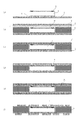
以下、本発明の実施例1にかかる半導体素子内蔵基板の製造方法について、図1を参照して説明する。図1は本発明の実施例1にかかる半導体素子内蔵基板の製造方法を示す断面図である。
【0030】
図1(a)に示すように、半導体素子としての半導体チップ1の裏面に絶縁性エポキシ樹脂4を設け、半導体チップ1を絶縁性エポキシ樹脂4を介して銅箔からなる第一のシート3の粗面化された面側に搭載する。
【0031】
第一のシートは導電性である事を有しないが、導電体である場合は公知のリソグラフィ技術を用いて第一のシートに配線パターンを容易に形成することが可能となる。
【0032】
その後、絶縁性エポキシ樹脂4を熱硬化させ、半導体チップ1を第一のシート3に接着させる。
【0033】
絶縁性エポキシ樹脂4の厚みは、接着に必要な強度を得ることが可能でなるならば、薄ければ薄いほど好ましいが、一般的には10〜30μmの範囲が良い。
【0034】
これよりも薄いと塗布時に均一な膜厚を確保することができず、気泡や未塗布の領域が発生してしまい、後の工程において剥離を発生させてしまう。
【0035】
また、これよりも厚いと半導体チップを固定する際に半導体チップが加圧力のばらつきにより傾斜して取り付くことになり、後の熱プレス工程において半導体チップの端部に高い応力が加わり半導体チップが破損してしまう。
【0036】
また、第一のシート3の厚みは8〜35μmの範囲が良い。
【0037】
これよりも薄いとハンドリングの際にシートが破断してしまったり、よれ、うねりを発生させてしまい安定して生産することができない。
【0038】
また、これよりも厚いと、この第1のシートに後に形成する配線を形成する際にエッチングにより微細な配線を形成することができなくなる。
【0039】
次に図1(b)に示すように半導体チップ1の厚み(通常50〜150μm程度)とほぼ同じ厚みをもち、半導体チップ1に対応する形状の開口部5aを打ち抜きプレスによって形成した第二のシート5をその開口部5aが半導体チップ1を収容する位置に配置する。
【0040】
第二のシート5は硬化反応途中の絶縁性樹脂であるエポキシ樹脂からなり、ガラスクロスが含まれたプリプレグ材を使用した。
【0041】
第二のシート5の上に、第三のシート7を載置する。
【0042】
第三のシート7として銅箔3’上に硬化反応途中の絶縁性樹脂としてのエポキシ樹脂6をコーティングしたRCC(レジンコーテッドカッパー)材を用いた。
【0043】
エポキシ樹脂6の厚みは10〜60μmの範囲が良い。
【0044】
これよりも薄いと半導体チップ上面の微細な凹凸を埋め込みその上の導体層である銅箔3‘との層間絶縁性が保たれなくなったり、未充填部が発生し、後にその未充填部から剥離を発生させてしまう。
【0045】
また、これよりも厚いと後の工程で半導体チップ電極との接続を行う際に電極部上に形成する穴のアスペクト比(穴径 対 深さ)が1以上となってしまい、非常に加工性が下がってしまう。
【0046】
なお、第三のシート7には硬化反応途中の絶縁性樹脂は必ずしも無くて良い。
【0047】
硬化反応性の樹脂を有する場合は、樹脂量を増やすことにより、銅箔との密着強度をより高く得ることができるとともに、未充填の発生頻度を抑えることができる。
【0048】
このように積み重ねて配置した上記のシートに真空雰囲気にて熱圧着をおこなう。このときの加熱温度は150〜200℃の温度が好ましい。
【0049】
熱圧着により、第二のシート5中のエポキシ樹脂と第三のシート7のエポキシ樹脂6が溶融し、半導体チップ1を図1(c)にあるように両面が銅箔に覆われたエポキシ樹脂中に埋め込んでしまう。
【0050】
このとき、第二のシート5としてガラスクロス入りのプリプレグ材を使用するのは、熱圧着時の圧力により半導体チップ1が存在する場所と存在しない場所での圧力差によりプレス後の表面の平坦性が損なわれるのを防ぐためである。
【0051】
従って、ガラスクロスの厚みは半導体チップの厚みと等しいか若干厚い方が好ましい。
【0052】
次に、図1(d)にあるように半導体チップ1の電極部2の位置に該当する部分の銅箔3’を通常のエッチングで除去し、その後、この穴部に露出する絶縁樹脂をCO2あるいは、YAG、エキシマといったレーザーにより除去し、半導体チップ1の電極部2が露出するようVia穴8を形成する。なお、半導体チップ1の電極部2は、Al上にTi/Niの拡散バリア層をあらかじめウェハー工程にて作りこんでおく。
【0053】
つぎに、Via穴8のクリーニングを過マンガン酸等により行い、図1(e)に示すようにメッキ工程にて全面に銅層3aを析出させる。これにより電極部2と銅箔3’とが接続される。
【0054】
次に、銅層3aとにレジスト材を塗り、露光・現像工程によりパターンをエッチングで形成し、図1(f)のような半導体チップ1が内蔵された両面配線回路基板を得る。このような両面配線回路基板は、多層配線回路基板を製造する際の基本構成であることから、次に述べるような多層化が容易に行える。
【0055】
図2に示すように、このような両面配線回路基板を間にプリプレグ材を介し、再度熱圧着をおこない、ドリルによる穴あけとメッキによるスルーホール9を形成することで、容易に多層化は可能となる。
【0056】
また、積層させるものは、両面配線回路基板である必要はなく、プリプレグ材と銅箔とを本発明の両面配線回路基板の両面に配置し、熱圧着を行えば4層配線基板が形成される。
【0057】
このように形成された半導体チップ1内蔵の回路基板は従来の回路基板と同じ工程により製造されているので、従来と同様に電子回路部品を表面に実装が可能であり、半導体チップ1が埋め込まれた半導体素子内蔵基板が容易に製造される。
【0058】
(実施例2)
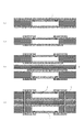
図3は本発明の実施例2にかかる回路基板の製造方法を示す断面図である。
【0059】
本実施例においては、図3(a)に示すように、配線21が形成された基板10上に半導体チップ1を実施例と同様に搭載し、接着させる。そして、第1の実施例と同様にプリプレグ材とRCC材を用い、半導体チップを熱圧着により回路基板中に埋め込む。
【0060】
次に、図3(d)に示すように従来のビルドアップ基板の製造方法と同様に、銅箔3’上のビア穴を形成する位置にウィンドを形成し、レーザー光により絶縁層部にビア穴8、11を形成する。その際、層間部22を形成する際と半導体チップ1の電極部2を形成する際のレーザー光のスポット径を変えることにより、それぞれに適した穴径サイズを形成する。
【0061】
次に、メッキ工程により、図3(e)にあるように層間、半導体チップ1の電極部2とを接続し、その後、露出している銅にエッチングによりパターンを形成させる。
【0062】
この工程を複数回繰り返せば、容易に多層化が図られることは、明らかである。
【0063】
本実施例によれば、ビルドアップ基板の製造プロセスを用いることにより、層間接続にスルーホールでなくビアを使用するので、より高密度な回路基板を製造することが可能である。そのため、より高密度な実装による製品の小型化が可能となる。
【0064】
(実施例3)
図4は、本発明の実施例3にかかる回路基板の製造方法を示す断面図である。
【0065】
本実施例においては、半導体チップ1の電極部2を有する面を先に銅箔3と絶縁性エポキシ樹脂12を用いて接着する。このエポキシ樹脂12には、シリカ粒子が分散されており、熱伝導性の向上と、水分吸収率の低減と、熱膨張係数がエポキシ樹脂単独の50ppmレベルから10〜30ppmへと低減することで半導体チップ表面にかかる熱応力の緩和を図ることが可能となっている。さらに、一括の熱プレスでの接着ではなく、半導体チップ1を個別に接着させるため、半導体チップ表面と銅箔3との間隔の制御が容易に行える。そのため、レーザーによる穴加工時のアスペクト比のばらつきがなく、より微細な穴径での加工ができ、より狭ピッチ多ピンの半導体チップに対応することが可能となる。
【0066】
その他の製造方法は、実施例1と同様である。
【0067】
(実施例4)
図5は、本発明の第4の実施例を示す模式的断面図である。
【0068】
本実施例においては、保持用の絶縁性基材からなる基板13上に半導体チップ1を搭載し、プリプレグ材5とRCC材7を介して一括熱プレスで半導体チップを埋設した後に、RCC材の銅箔3’を全面で剥離する。その後レーザーにて、半導体チップ1の電極部2上にVia穴を設け、クリーニングした後全面にメッキにより銅を設ける。
【0069】
その後、エッチングによりパターンを形成する。本実施例では、RCC材の銅箔厚みがなく、メッキのみの厚みとなることから、より微細な配線パターンの形成が可能となる。
【0070】
そして、パターン形成後、はんだレジスト層を設け、露出する銅パターンのランド部にはんだボール14を搭載することで、半導体チップ内蔵の極めて薄いパッケージを提供することが可能となる。
【0071】
さらに、スーパーCSP等のチップサイズ上だけしか接続用Padを設けることができないといった制約は、ないので、接続Pad数を満たした小型パッケージを容易に提供することが可能である。
【0072】
また、本実施例では、保持用に絶縁性基材からなる基板13を使用したが、熱伝導性の高い金属プレートを保持用に使用することも可能であり、この構成時には極めて放熱性の高いパッケージとなる。
【0073】
本実施例では、通常のCSPやBGAパッケージのインターポーザー(中間基板)を別に製造するのではなく、インターポーザー製造と半導体チップの接続・封止工程を一括しておこなってしまう。そのため、非常に多くの工程数を削減でき、タクト時間の短縮、製造コストの削減をすることが可能となる。
【0074】
(実施例5)
図6は、本発明の第5の実施例を示す模式的断面図である。
【0075】
本実施例においては、上記第4の実施例による半導体チップが埋設され、パターンが形成された基板パッケージ16の状態でバーンイン試験を行い、良品のチップが内蔵される基板パッケージ16を判別する。そして、半導体チップが埋設された別の基板パッケージ16’の一方の面に形成された配線ランド部にはんだペースト17を印刷により設け、その後にこのランド部の位置に対向する位置にランド部が設けれているバーンイン試験で良品と判定された基板パッケージ16を位置合わせの後搭載し、リフロー工程によりはんだペースト17を溶融させ、基板パッケージの各ランド部間を接続する。
【0076】
次に、この接続された基板パッケージの一方の面にあるランド部にはんだボール14を搭載し、再びリフローによりはんだボール14とランドとを接続し、パッケージ上にパッケージが実装された複合パッケージが正蔵される。
【0077】
なお、本実施例では、半導体チップ内蔵基板パッケージ同士の組み合わせであったが、複数個のものを同様に組み合わせてもかまわない。
【0078】
さらに、より汎用性の高い半導体チップと組み合わせる場合には、基板パッケージの接続用ランド部のデザインを汎用品のパッケージのランドデザインに合わせることで対応は、可能となる。
【0079】
本実施例では、試験後の良品チップ内蔵のパッケージ同士を組み合わせることが可能となるため、不良混入による歩留まり低下を排除でき、かつ基板内部に半導体チップが埋め込まれていることから、パッケージを組み合わせても実装後の厚みは、極めて薄い複合パッケージを提供することが可能となる。
【0080】
また、より薄い複合パッケージを求めるのであれば,図7に示すような不良率の高い半導体チップを基板内に埋め込み試験をおこない、その上で、良品と判断されたものにのみ、通常の半導体パッケージを製造するのと同様に半導体チップを搭載し、ワイヤーボンダーで接続しトランスファーモールドで封止をおこない、はんだボール14を接続後、ダイシングソーにて個々のパッケージに切断することも可能である。
【0081】
この方式では、通常のスタック構造より配線自由度、搭載チップサイズ自由度が大幅に高まるだけでなく、不良率の高い半導体チップに対しては中間検査を行えることか、より高い歩留まりを得ることができる。
【0082】
【発明の効果】
以上述べてきたように、本発明では、半導体素子を基板製造工程中に一括した熱圧着工程にて基板内部に埋め込み、配線形成と合わせて接続することにより、半導体素子を基板内に精度良く埋め込み配置する事ができるとともに、大幅な製造工程の短縮が可能となる。
【0083】
さらに、基板内部に埋め込まれ、パターンが形成されればバーンイン試験等の後工程試験は容易におこなうことが可能となることから、良品選別が可能であり、より複合化された場合であっても高い歩留まりを維持でき、低コスト化が可能となる。
【0084】
また、配線設計自由度が高いことから、様々な半導体チップあるいは、電気回路部品との組み合わせに柔軟に対応することが可能であり、より高機能かつ小型の製品をローコストで提供することが可能となる。
【図面の簡単な説明】
【図1】第1の実施例を示す模式的断面製造図
【図2】第1の実施例の多層化を示す模式的断面製造図
【図3】第2の実施例を示す模式的断面製造図
【図4】第3の実施例を示す模式的断面製造図
【図5】第4の実施例を示す模式的断面製造図
【図6】第5の実施例を示す模式的断面製造図
【図7】第5の実施例を示す模式的断面製造図
【図8】従来例を示す模式的断面製造図
【符号の説明】
1 半導体チップ
2 半導体チップの電極部
3 銅箔
4 絶縁性接着剤
5 プリプレグ材
6 エポキシ樹脂(Bステージ状態)
7 RCC
8 ビア穴
9 スルーホール
10 配線基板
11 ビア穴(層間接続用)
12 フィラー含有エポキシ樹脂
13 保持用基板
14 はんだボール
15 基板パッケージ
16 ランド部
17 はんだペースト
18 金ワイヤー
19 封止モールド
20 凹部[0001]
BACKGROUND OF THE INVENTION
The present invention relates to a method for manufacturing a substrate with a built-in semiconductor element in which an electric circuit component is mounted on a circuit board.
[0002]
[Prior art]
In recent years, in order to reduce the size and weight of electronic device products, it is desired to reduce the size of a substrate with a built-in semiconductor element incorporated in the electronic device product.
[0003]
As a means for downsizing a conventional substrate with a built-in semiconductor element, a frame material having a hole made of prepreg is press-laminated on a bottom plate to form a substrate having a recess, and then a semiconductor chip is attached to the recess and then crimped. In addition, a method has been proposed in which an insulating layer or a wiring layer is further formed thereon, and an electric circuit component is further mounted thereon (see, for example, Patent Document 1).
A method of sequentially stacking semiconductor chips on a circuit board has been proposed. (For example, refer to Patent Document 2.)
Furthermore, a method has been proposed in which bumps are formed on electrode portions of a semiconductor chip, an insulating resin is applied, embedded, and polished. (For example, refer to Patent Document 3.)
[Patent Document 1]
JP 2002-16173 A (page 4)
[Patent Document 2]
JP-A-5-13967 [Patent Document 3]
Japanese Patent Laid-Open No. 2002-290006
[Problems to be solved by the invention]
However, the invention described in JP-A-2002-16173 has the following problems.
[0005]
In the pressing process when laminating the substrates, the pressing pressure becomes non-uniform, resulting in insufficient adhesion, and the shape of the recesses becomes non-uniform. In particular, when a hot press is used, the resin in the prepreg is softened by the hot pressing process and flows into the recesses, and the bottom of the recesses has large unevenness, or in the worst case, the recesses are buried, and the semiconductor chip is mounted later. The shape of the recess necessary for placement cannot be maintained.
[0006]
In order to embed a semiconductor chip, a holding surface for holding the semiconductor chip must be formed at the bottom of the concave portion of the circuit board, and an insulating layer for the holding surface is required. In this case, the thickness of the insulating layer between the conductor layers sandwiching the semiconductor chip is very thick because the thickness of the semiconductor chip is added to the thickness of the insulating layer on the holding surface. Therefore, when a semiconductor chip is embedded between a plurality of layers of a circuit board composed of a plurality of layers, the layer thickness of the circuit board becomes extremely thick and cannot be reduced in size.
[0007]
Further, in the method of incorporating the semiconductor chip after forming the recesses and embedding after that, the recesses must be formed for each layer when the number of layers is increased, and the production efficiency is extremely low.
[0008]
Further, in a method in which such a recess is provided in a substrate and a semiconductor chip is mounted therein, and then a liquid insulating resin is used to cover the semiconductor chip, the amount of resin when the insulating resin cures and shrinks is in-plane. Since they are different, it is difficult to obtain uniformity and flatness of the surface of the insulating resin after curing. For this reason, the resist image is disturbed in the exposure, development, and etching steps, and a fine wiring pattern cannot be formed. In particular, around the semiconductor chip, since the resin corresponding to the chip thickness cures and shrinks, the surface tends to be concave.
[0009]
In the case of a method of embedding without forming a concave portion, a bonding process for connecting the electrode portion of the wiring pattern formed in advance on the surface of the substrate and the electrode portion of the semiconductor chip is indispensable.
[0010]
As a method of performing this connection, when performing flip chip connection, it is necessary to form solder bumps or balls on the electrode pad portions of the semiconductor chip.
And after aligning the solder bump of this semiconductor chip and the electrode part of the wiring pattern of a board | substrate, a semiconductor chip is mounted on a pattern electrode and it joins by heating. Further, a complicated bonding process is required in which a connection reinforcing resin called an underfill material is injected and fixed between gaps formed by bumps between the semiconductor chip surface and the substrate surface.
[0011]
Furthermore, if such a flip chip connection is to be made with a semiconductor chip that will increase in the number of pins in the future, not only will the bumps and solder balls formed on the semiconductor chip be required to be finer and more precise, Substrate wiring pitch is also required to be finer. As a result, bump formation costs and substrate costs increase significantly. In addition, the positioning accuracy at the time of mounting is required to be stricter, leading to an increase in apparatus cost.
[0012]
In the method of laminating sequentially, the electrode portions of the semiconductor chip must always face in the same plane direction. Therefore, in order to connect between the semiconductor chips, it is necessary to make the thickness of the semiconductor chip at least as short as possible, and it is difficult to shorten the wiring length. For this reason, when a signal is transmitted at a higher speed, the signal waveform is delayed or the waveform shape is disturbed, and it is difficult to transmit the signal at a high speed.
[0013]
In addition, in order to connect the wiring from the electrode part of each semiconductor chip stacked on the semiconductor chip, the size of the semiconductor chip stacked on the semiconductor chip must be smaller than the semiconductor chip below it. However, there is a design constraint that each semiconductor chip to be stacked is limited by its size.
[0014]
In the method of forming bumps on the electrode part of the semiconductor chip, applying insulating resin, embedding and polishing, the polishing process is always performed to remove the insulating resin covering the bumps and to flatten the surface of the insulating resin Is required. On the other hand, when the stud bump is exposed by a laser, if the laser beam hits a stud bump made of gold with high reflectivity and a neck-cut shape with poor stability, the laser beam is reflected and scattered and the shape of the processed hole is remarkable. Deteriorate. For this reason, it is impossible to perform stable connection hole processing for the electrode portion pitch of a semiconductor chip having a very narrow pitch of 100 μm or less.
[0015]
Further, the method of providing bumps larger than the semiconductor chip electrode area on the semiconductor chip for relaxing the hole machining accuracy cannot cope with the narrowing of the inter-electrode pitch accompanying the increase in the number of electrodes of the semiconductor chip. In addition, a bump forming process is required only for the positional accuracy at the time of drilling, resulting in an increase in cost.
[0016]
[Means for Solving the Problems]
A first method for manufacturing a substrate with a built-in semiconductor element according to the present invention is a method for manufacturing a substrate with a built-in semiconductor element in which a semiconductor element is embedded in a circuit board.
Bonding the semiconductor element to the first sheet;
Placing a second sheet made of an insulating resin in the middle of the curing reaction and having an opening on the first sheet so that the semiconductor element is accommodated in the opening;
Placing a third sheet made of a conductor on the second sheet;
A step of thermocompression bonding the first, second and third sheets together;
Removing the portion of the second and third sheets located immediately above the electrode portion of the semiconductor element;
Electrically connecting the electrode part and the third sheet;
And processing the third sheet into a pattern to form a wiring.
[0017]
The second method for manufacturing a substrate with a built-in semiconductor element according to the present invention is characterized in that, in the first manufacturing method, the third sheet has an insulating resin in the middle of the curing reaction on the side facing the second sheet. It is what.
[0018]
According to the third method for manufacturing a substrate with a built-in semiconductor element according to the present invention, in the first manufacturing method, in the step of bonding the semiconductor element to the first sheet, the surface side having the electrode portion of the semiconductor element is the surface side. It is characterized by adhering to the first sheet.
[0019]
According to the fourth method for manufacturing a substrate with a built-in semiconductor element according to the present invention, in the first manufacturing method, an insulating resin containing inorganic particles is used as an adhesive member in the step of bonding the semiconductor element to the first sheet. It is characterized by using.
[0020]
According to a fifth aspect of the present invention, in the first manufacturing method, the second sheet includes a material that does not melt or flow at a heating temperature in the thermocompression bonding step. To do.
[0021]
Compared to the conventional method for manufacturing a semiconductor element embedded substrate, the following various effects can be obtained.
[0022]
The present invention does not require a step of providing a recess in a completed or semi-finished circuit board, and embeds the semiconductor element in the circuit board by thermocompression bonding a plurality of stacked sheets and semiconductor elements at once. The process can be greatly shortened and the cost can be reduced. Furthermore, since it is not necessary to provide an insulating layer portion for mounting and holding the semiconductor element, it is possible to reduce the thickness after the semiconductor element is embedded.
[0023]
In addition, the conventional problem of rewiring even a defective semiconductor element when performing rewiring on a semiconductor wafer, the electrode can be expanded only on the semiconductor element, and cannot cope with the increase in the number of pins. The problem can be solved easily.
[0024]
Furthermore, regarding the burn-in inspection in the case of stacking a plurality of semiconductor elements, if the semiconductor elements are built in and wiring is formed, the electrode terminal pitch of the test jig can be sufficiently accommodated and the cost is not increased. An inspection can be easily performed. Therefore, it is possible to combine non-defective products after inspection, and it is possible to provide a connection electrode on the substrate regardless of the size of the built-in semiconductor element. Thus, it is possible to combine semiconductor elements.
[0025]
Furthermore, a general-purpose IC should be mounted on the package by providing an electrode for connecting the system board on one side of the double-sided circuit board containing the semiconductor element and an electrode for general-purpose IC on the other side. Therefore, the degree of freedom of design that can easily cope with various specification changes for each product is greatly increased.
[0026]
In addition, since the second sheet surrounding the semiconductor element is formed as an insulating layer having uniform material characteristics by the thermocompression bonding process, the generation of warpage and undulation of the entire semiconductor element-embedded substrate is suppressed. It is possible to form a wiring pattern.
[0027]
Furthermore, since a pattern can be easily formed directly under the back surface of the semiconductor element, heat dissipation can be enhanced by using this pattern as a heat spreader for heat dissipation.
[0028]
Moreover, by preparing double-sided substrates each incorporating the semiconductor element as described above and further laminating them, it is possible to easily cope with various circuit configurations.
[0029]
DETAILED DESCRIPTION OF THE INVENTION
Example 1
Hereinafter, a manufacturing method of a semiconductor element embedded substrate according to Example 1 of the present invention will be described with reference to FIG. 1 is a cross-sectional view showing a method of manufacturing a substrate with a built-in semiconductor element according to
[0030]
As shown in FIG. 1A, an insulating
[0031]
The first sheet does not have conductivity, but when it is a conductor, a wiring pattern can be easily formed on the first sheet using a known lithography technique.
[0032]
Thereafter, the insulating
[0033]
The thickness of the insulating
[0034]
If it is thinner than this, a uniform film thickness cannot be ensured at the time of coating, bubbles and uncoated areas are generated, and peeling occurs in a later step.
[0035]
If it is thicker than this, the semiconductor chip will be tilted and attached due to variations in the applied pressure when fixing the semiconductor chip, and the semiconductor chip will be damaged due to high stress applied to the edge of the semiconductor chip in the subsequent hot pressing process. Resulting in.
[0036]
The thickness of the first sheet 3 is preferably in the range of 8 to 35 μm.
[0037]
If it is thinner than this, the sheet may break during handling, or it may be twisted or swollen, and stable production cannot be achieved.
[0038]
On the other hand, if it is thicker than this, fine wiring cannot be formed by etching when forming wiring to be formed later on the first sheet.
[0039]
Next, as shown in FIG. 1 (b), a second portion in which an opening 5a having a thickness substantially equal to the thickness of the semiconductor chip 1 (usually about 50 to 150 μm) and corresponding to the
[0040]
The second sheet 5 was made of an epoxy resin that is an insulating resin in the middle of the curing reaction, and a prepreg material containing glass cloth was used.
[0041]
A
[0042]
As the
[0043]
The thickness of the
[0044]
If it is thinner than this, fine irregularities on the upper surface of the semiconductor chip are embedded, and the interlayer insulation with the copper foil 3 ′, which is the conductor layer thereon, cannot be maintained, or an unfilled part is generated, which is later peeled off from the unfilled part Will be generated.
[0045]
On the other hand, if it is thicker than this, the aspect ratio (hole diameter to depth) of the hole formed on the electrode part when connecting to the semiconductor chip electrode in a later process becomes 1 or more, which is very workable. Will go down.
[0046]
The
[0047]
In the case of having a curing reactive resin, by increasing the amount of resin, it is possible to obtain higher adhesion strength with the copper foil and to suppress the occurrence frequency of unfilling.
[0048]
The above-described sheets arranged in a stacked manner are subjected to thermocompression bonding in a vacuum atmosphere. The heating temperature at this time is preferably 150 to 200 ° C.
[0049]
The epoxy resin in the second sheet 5 and the
[0050]
At this time, the glass sheet-containing prepreg material is used as the second sheet 5 because of the difference in pressure between the place where the
[0051]
Therefore, the thickness of the glass cloth is preferably equal to or slightly thicker than the thickness of the semiconductor chip.
[0052]
Next, as shown in FIG. 1 (d), the copper foil 3 'corresponding to the position of the electrode portion 2 of the
[0053]
Next, the via hole 8 is cleaned with permanganic acid or the like, and a copper layer 3a is deposited on the entire surface in a plating step as shown in FIG. 1 (e). Thereby, the electrode part 2 and copper foil 3 'are connected.
[0054]
Next, a resist material is applied to the copper layer 3a, and a pattern is formed by etching by an exposure / development process, thereby obtaining a double-sided wiring circuit board in which the
[0055]
As shown in FIG. 2, such a double-sided wiring circuit board is subjected to thermocompression bonding again with a prepreg material in between, and drilling and plating through-
[0056]
Moreover, what is laminated does not need to be a double-sided wiring circuit board, and a four-layer wiring board is formed by placing prepreg material and copper foil on both sides of the double-sided wiring circuit board of the present invention and performing thermocompression bonding. .
[0057]
Since the circuit board with the built-in
[0058]
(Example 2)
FIG. 3 is a sectional view showing a circuit board manufacturing method according to the second embodiment of the present invention.
[0059]
In the present embodiment, as shown in FIG. 3A, the
[0060]
Next, as shown in FIG. 3 (d), a window is formed at a position where a via hole is to be formed on the copper foil 3 ', and a via is formed in the insulating layer portion by laser light, as in the conventional build-up board manufacturing method. Holes 8 and 11 are formed. At that time, by changing the spot diameter of the laser beam when forming the
[0061]
Next, as shown in FIG. 3E, the interlayer and the electrode portion 2 of the
[0062]
Obviously, if this process is repeated a plurality of times, the number of layers can be easily increased.
[0063]
According to the present embodiment, by using a build-up substrate manufacturing process, vias are used for interlayer connection instead of through-holes, so that a higher-density circuit board can be manufactured. Therefore, it is possible to reduce the size of the product by mounting with higher density.
[0064]
(Example 3)
FIG. 4 is a cross-sectional view showing a method for manufacturing a circuit board according to Example 3 of the present invention.
[0065]
In this embodiment, the surface having the electrode portion 2 of the
[0066]
Other manufacturing methods are the same as those in the first embodiment.
[0067]
Example 4
FIG. 5 is a schematic sectional view showing a fourth embodiment of the present invention.
[0068]
In the present embodiment, the
[0069]
Thereafter, a pattern is formed by etching. In the present embodiment, there is no thickness of the copper foil of the RCC material, and only the thickness of the plating is obtained, so that a finer wiring pattern can be formed.
[0070]
Then, by providing a solder resist layer after pattern formation and mounting the
[0071]
Furthermore, since there is no restriction that the connection pad can be provided only on the chip size of a super CSP or the like, it is possible to easily provide a small package satisfying the number of connection pads.
[0072]
In the present embodiment, the
[0073]
In the present embodiment, the interposer manufacturing and the semiconductor chip connection / sealing process are performed in a lump, instead of manufacturing a normal CSP or BGA package interposer (intermediate substrate) separately. Therefore, a very large number of processes can be reduced, and the tact time can be shortened and the manufacturing cost can be reduced.
[0074]
(Example 5)
FIG. 6 is a schematic sectional view showing a fifth embodiment of the present invention.
[0075]
In the present embodiment, the burn-in test is performed in the state of the
[0076]
Next, the
[0077]
In the present embodiment, the combination of semiconductor chip built-in substrate packages is used, but a plurality of packages may be combined in the same manner.
[0078]
Further, when combined with a semiconductor chip having higher versatility, it is possible to cope with this by matching the design of the connection land portion of the substrate package with the land design of the general-purpose product package.
[0079]
In this example, since it is possible to combine packages with good chips after the test, it is possible to eliminate a decrease in yield due to mixing of defects, and semiconductor chips are embedded inside the substrate. In addition, it becomes possible to provide a composite package having a very thin thickness after mounting.
[0080]
If a thinner composite package is desired, a semiconductor chip with a high defect rate as shown in FIG. 7 is embedded in the substrate, and only those that are determined to be non-defective products are subjected to normal semiconductor packages. It is also possible to mount a semiconductor chip in the same manner as in manufacturing, connect with a wire bonder, seal with a transfer mold, connect the
[0081]
In this method, not only the degree of freedom of wiring and the size of the mounted chip is greatly increased compared to the normal stack structure, but it is also possible to perform intermediate inspection on a semiconductor chip with a high defect rate or to obtain a higher yield. it can.
[0082]
【The invention's effect】
As described above, in the present invention, the semiconductor element is embedded in the substrate with high accuracy by embedding the semiconductor element in the substrate in a batch thermocompression bonding process during the substrate manufacturing process and connecting with the wiring formation. It can be arranged and the manufacturing process can be greatly shortened.
[0083]
Furthermore, since it is possible to easily perform post-process tests such as a burn-in test if the pattern is formed inside the substrate, it is possible to select non-defective products, even if they are more complex. High yields can be maintained and costs can be reduced.
[0084]
In addition, since the degree of freedom in wiring design is high, it is possible to flexibly respond to combinations with various semiconductor chips or electrical circuit components, and it is possible to provide more sophisticated and compact products at low cost. Become.
[Brief description of the drawings]
FIG. 1 is a schematic cross-sectional manufacturing view showing a first embodiment. FIG. 2 is a schematic cross-sectional manufacturing view showing multi-layering of the first embodiment. FIG. 3 is a schematic cross-sectional manufacturing view showing a second embodiment. FIG. 4 is a schematic cross-sectional manufacturing view showing a third embodiment. FIG. 5 is a schematic cross-sectional manufacturing view showing a fourth embodiment. FIG. 6 is a schematic cross-sectional manufacturing view showing a fifth embodiment. FIG. 7 is a schematic cross-sectional manufacturing view showing a fifth embodiment. FIG. 8 is a schematic cross-sectional manufacturing view showing a conventional example.
DESCRIPTION OF
7 RCC
8 Via
12 Filler-containing
Claims (5)
第一のシートに前記半導体素子を接着する工程と、
硬化反応途中の絶縁性樹脂からなり開口部を有する第二のシートを、前記開口部中に前記半導体素子が収容されるように前記第一のシート上に載置する工程と、
導電体からなる第三のシートを前記第二のシート上に載置する工程と、
前記第一、第二及び第三のシートを一括して熱圧着する工程と、
前記第二及び第三のシートの、前記半導体素子の電極部直上に位置する部分を除去する工程と、
前記電極部と前記第三のシートとを電気的に接続する工程と、
前記第三のシートをパターン状に加工し配線を形成する工程と、を有することを特徴とする半導体素子内蔵基板の製造方法。In a method for manufacturing a semiconductor element embedded substrate in which a semiconductor element is embedded in a circuit board,
Bonding the semiconductor element to the first sheet;
Placing a second sheet made of an insulating resin in the middle of the curing reaction and having an opening on the first sheet so that the semiconductor element is accommodated in the opening;
Placing a third sheet of conductor on the second sheet;
A step of thermocompression bonding the first, second and third sheets together;
Removing the portion of the second and third sheets located immediately above the electrode portion of the semiconductor element;
Electrically connecting the electrode portion and the third sheet;
And a step of processing the third sheet into a pattern to form a wiring.
Priority Applications (1)
| Application Number | Priority Date | Filing Date | Title |
|---|---|---|---|
| JP2003127990A JP2004335641A (en) | 2003-05-06 | 2003-05-06 | Method of manufacturing substrate having built-in semiconductor element |
Applications Claiming Priority (1)
| Application Number | Priority Date | Filing Date | Title |
|---|---|---|---|
| JP2003127990A JP2004335641A (en) | 2003-05-06 | 2003-05-06 | Method of manufacturing substrate having built-in semiconductor element |
Publications (1)
| Publication Number | Publication Date |
|---|---|
| JP2004335641A true JP2004335641A (en) | 2004-11-25 |
Family
ID=33504305
Family Applications (1)
| Application Number | Title | Priority Date | Filing Date |
|---|---|---|---|
| JP2003127990A Withdrawn JP2004335641A (en) | 2003-05-06 | 2003-05-06 | Method of manufacturing substrate having built-in semiconductor element |
Country Status (1)
| Country | Link |
|---|---|
| JP (1) | JP2004335641A (en) |
Cited By (53)
| Publication number | Priority date | Publication date | Assignee | Title |
|---|---|---|---|---|
| JP2006196785A (en) * | 2005-01-14 | 2006-07-27 | Dainippon Printing Co Ltd | Printed-wiring board having built-in electronic component and manufacturing method thereof |
| JP2006261246A (en) * | 2005-03-15 | 2006-09-28 | Shinko Electric Ind Co Ltd | Wiring circuit board and manufacturing method thereof |
| JP2006261245A (en) * | 2005-03-15 | 2006-09-28 | Shinko Electric Ind Co Ltd | Manufacturing method of wiring circuit board |
| JP2006269594A (en) * | 2005-03-23 | 2006-10-05 | Cmk Corp | Semiconductor device and manufacturing method thereof |
| KR100643334B1 (en) | 2005-11-09 | 2006-11-10 | 삼성전기주식회사 | Chip embedded pcb and the method for manufacturing the same |
| KR100651474B1 (en) | 2005-08-29 | 2006-11-29 | 삼성전기주식회사 | Manufacturing method of pcb for embedded chip |
| JP2006351778A (en) * | 2005-06-15 | 2006-12-28 | Ngk Spark Plug Co Ltd | Manufacturing method of wiring board |
| JP2007053360A (en) * | 2005-08-15 | 2007-03-01 | Phoenix Precision Technology Corp | Laminate structure of semiconductor element-padding support plate |
| KR100688769B1 (en) * | 2004-12-30 | 2007-03-02 | 삼성전기주식회사 | Embedded chip print circuit board and method for fabricating the same by means of plating |
| KR100704935B1 (en) | 2005-06-28 | 2007-04-09 | 삼성전기주식회사 | Chip embedded PCB and method of the same |
| KR100704936B1 (en) | 2005-06-22 | 2007-04-09 | 삼성전기주식회사 | Printed Circuit Board Having Embedded Electronic Parts and Methods of Fabrication therefor |
| KR100704930B1 (en) | 2005-06-24 | 2007-04-09 | 삼성전기주식회사 | Printed Circuit Board Having Embedded Capacitor and Fabricating Method thereof |
| KR100704934B1 (en) * | 2005-06-27 | 2007-04-10 | 삼성전기주식회사 | Multi-layer Printed Circuit Board Having Embedded Condenser and Fabricating Method therefor |
| KR100758229B1 (en) | 2006-04-11 | 2007-09-12 | 삼성전기주식회사 | Electronic components embedded pcb and the method for manufacturing thereof |
| KR100773985B1 (en) | 2006-06-19 | 2007-11-08 | 삼성전기주식회사 | Manufacturing method electronic components embedded pcb |
| KR100811034B1 (en) | 2007-04-30 | 2008-03-06 | 삼성전기주식회사 | Method for manufacturing printed circuit board having embedded electronic components |
| KR100821154B1 (en) * | 2007-07-11 | 2008-04-14 | 삼성전기주식회사 | Electronic components embedded PCB and the method for manufacturing thereof |
| JP2008522397A (en) * | 2004-11-26 | 2008-06-26 | イムベラ エレクトロニクス オサケユキチュア | Electronic module and manufacturing method thereof |
| JP2008198999A (en) * | 2007-02-15 | 2008-08-28 | Samsung Electro Mech Co Ltd | Printed circuit board with built-in electronic device and method of manufacturing the same |
| KR100859004B1 (en) * | 2007-08-22 | 2008-09-18 | 삼성전기주식회사 | Manufacturing method of electro-component embedded pcb |
| JP2008251745A (en) * | 2007-03-29 | 2008-10-16 | Sanyo Electric Co Ltd | Circuit device and manufacturing method thereof |
| KR100926657B1 (en) * | 2008-04-22 | 2009-11-17 | 대덕전자 주식회사 | Wafer-level packaged printed circuit boards and manufacturing methods |
| JP2010098286A (en) * | 2008-10-20 | 2010-04-30 | Samsung Electro-Mechanics Co Ltd | Printed circuit board and its manufacturing method |
| KR100957744B1 (en) | 2008-07-11 | 2010-05-12 | 대덕전자 주식회사 | Method of fabricating bumpless chip embedded printed circuit board |
| JPWO2008093531A1 (en) * | 2007-01-29 | 2010-05-20 | 日本電気株式会社 | Semiconductor device and manufacturing method thereof |
| JP2010153767A (en) * | 2008-12-24 | 2010-07-08 | Ibiden Co Ltd | Wiring board and method of manufacturing the same |
| WO2011016555A1 (en) * | 2009-08-07 | 2011-02-10 | 日本電気株式会社 | Semiconductor device and method for manufacturing same |
| JP2011517858A (en) * | 2008-04-18 | 2011-06-16 | インベラ エレクトロニクス オサケユキチュア | Wiring board and method for manufacturing the wiring board |
| JP2012199342A (en) * | 2011-03-20 | 2012-10-18 | Fujitsu Ltd | Method for manufacturing resin-molded substrate, and resin-molded substrate |
| WO2013038468A1 (en) * | 2011-09-12 | 2013-03-21 | 株式会社メイコー | Method for manufacturing substrate with built-in component and substrate with built-in component using same |
| JP2013093614A (en) * | 2010-05-25 | 2013-05-16 | Samsung Electro-Mechanics Co Ltd | Embedded printed circuit board and method of manufacturing the same |
| US8450844B2 (en) | 2010-01-07 | 2013-05-28 | Samsung Electro-Mechanics Co., Ltd. | Semiconductor package and method of manufacturing the same |
| US8536691B2 (en) | 2006-11-06 | 2013-09-17 | Renesas Electronics Corporation | Semiconductor device and method for manufacturing the same |
| US8609539B2 (en) | 2005-11-02 | 2013-12-17 | Canon Kabushiki Kaisha | Embedded semiconductor device substrate and production method thereof |
| JP5456970B2 (en) * | 2005-02-02 | 2014-04-02 | 日本電気株式会社 | Electronic component packaging structure and method of manufacturing electronic component package having this structure |
| KR20140075357A (en) * | 2012-12-11 | 2014-06-19 | 삼성전기주식회사 | Chip embedded PCB(printed circuit board) and semiconductor package using the PCB, and manufacturing method of the PCB |
| KR20160095718A (en) * | 2015-02-03 | 2016-08-12 | 주식회사 심텍 | embedded PCB and method of manufacturing the same |
| JPWO2015198870A1 (en) * | 2014-06-23 | 2017-04-20 | 株式会社村田製作所 | Component built-in substrate and method for manufacturing component built-in substrate |
| KR101811941B1 (en) * | 2016-01-27 | 2017-12-26 | 주식회사 코리아써키트 | Embedded printed circuit board manufacturing method |
| CN110798991A (en) * | 2018-08-01 | 2020-02-14 | 宏启胜精密电子(秦皇岛)有限公司 | Embedded substrate, manufacturing method thereof and circuit board with embedded substrate |
| US10886232B2 (en) | 2019-05-10 | 2021-01-05 | Applied Materials, Inc. | Package structure and fabrication methods |
| US10937726B1 (en) | 2019-11-27 | 2021-03-02 | Applied Materials, Inc. | Package structure with embedded core |
| US11063169B2 (en) | 2019-05-10 | 2021-07-13 | Applied Materials, Inc. | Substrate structuring methods |
| US11232951B1 (en) | 2020-07-14 | 2022-01-25 | Applied Materials, Inc. | Method and apparatus for laser drilling blind vias |
| US11257790B2 (en) | 2020-03-10 | 2022-02-22 | Applied Materials, Inc. | High connectivity device stacking |
| US11342256B2 (en) | 2019-01-24 | 2022-05-24 | Applied Materials, Inc. | Method of fine redistribution interconnect formation for advanced packaging applications |
| US11404318B2 (en) | 2020-11-20 | 2022-08-02 | Applied Materials, Inc. | Methods of forming through-silicon vias in substrates for advanced packaging |
| US11400545B2 (en) | 2020-05-11 | 2022-08-02 | Applied Materials, Inc. | Laser ablation for package fabrication |
| US11454884B2 (en) | 2020-04-15 | 2022-09-27 | Applied Materials, Inc. | Fluoropolymer stamp fabrication method |
| US11521937B2 (en) | 2020-11-16 | 2022-12-06 | Applied Materials, Inc. | Package structures with built-in EMI shielding |
| US11676832B2 (en) | 2020-07-24 | 2023-06-13 | Applied Materials, Inc. | Laser ablation system for package fabrication |
| US11705365B2 (en) | 2021-05-18 | 2023-07-18 | Applied Materials, Inc. | Methods of micro-via formation for advanced packaging |
| US11931855B2 (en) | 2019-06-17 | 2024-03-19 | Applied Materials, Inc. | Planarization methods for packaging substrates |
-
2003
- 2003-05-06 JP JP2003127990A patent/JP2004335641A/en not_active Withdrawn
Cited By (76)
| Publication number | Priority date | Publication date | Assignee | Title |
|---|---|---|---|---|
| JP2008522397A (en) * | 2004-11-26 | 2008-06-26 | イムベラ エレクトロニクス オサケユキチュア | Electronic module and manufacturing method thereof |
| KR100688769B1 (en) * | 2004-12-30 | 2007-03-02 | 삼성전기주식회사 | Embedded chip print circuit board and method for fabricating the same by means of plating |
| JP2006196785A (en) * | 2005-01-14 | 2006-07-27 | Dainippon Printing Co Ltd | Printed-wiring board having built-in electronic component and manufacturing method thereof |
| JP5456970B2 (en) * | 2005-02-02 | 2014-04-02 | 日本電気株式会社 | Electronic component packaging structure and method of manufacturing electronic component package having this structure |
| JP2006261246A (en) * | 2005-03-15 | 2006-09-28 | Shinko Electric Ind Co Ltd | Wiring circuit board and manufacturing method thereof |
| JP2006261245A (en) * | 2005-03-15 | 2006-09-28 | Shinko Electric Ind Co Ltd | Manufacturing method of wiring circuit board |
| JP4526983B2 (en) * | 2005-03-15 | 2010-08-18 | 新光電気工業株式会社 | Wiring board manufacturing method |
| JP2006269594A (en) * | 2005-03-23 | 2006-10-05 | Cmk Corp | Semiconductor device and manufacturing method thereof |
| JP4714510B2 (en) * | 2005-06-15 | 2011-06-29 | 日本特殊陶業株式会社 | Wiring board manufacturing method |
| JP2006351778A (en) * | 2005-06-15 | 2006-12-28 | Ngk Spark Plug Co Ltd | Manufacturing method of wiring board |
| KR100704936B1 (en) | 2005-06-22 | 2007-04-09 | 삼성전기주식회사 | Printed Circuit Board Having Embedded Electronic Parts and Methods of Fabrication therefor |
| KR100704930B1 (en) | 2005-06-24 | 2007-04-09 | 삼성전기주식회사 | Printed Circuit Board Having Embedded Capacitor and Fabricating Method thereof |
| KR100704934B1 (en) * | 2005-06-27 | 2007-04-10 | 삼성전기주식회사 | Multi-layer Printed Circuit Board Having Embedded Condenser and Fabricating Method therefor |
| KR100704935B1 (en) | 2005-06-28 | 2007-04-09 | 삼성전기주식회사 | Chip embedded PCB and method of the same |
| JP2007053360A (en) * | 2005-08-15 | 2007-03-01 | Phoenix Precision Technology Corp | Laminate structure of semiconductor element-padding support plate |
| KR100651474B1 (en) | 2005-08-29 | 2006-11-29 | 삼성전기주식회사 | Manufacturing method of pcb for embedded chip |
| US8609539B2 (en) | 2005-11-02 | 2013-12-17 | Canon Kabushiki Kaisha | Embedded semiconductor device substrate and production method thereof |
| KR100643334B1 (en) | 2005-11-09 | 2006-11-10 | 삼성전기주식회사 | Chip embedded pcb and the method for manufacturing the same |
| KR100758229B1 (en) | 2006-04-11 | 2007-09-12 | 삼성전기주식회사 | Electronic components embedded pcb and the method for manufacturing thereof |
| KR100773985B1 (en) | 2006-06-19 | 2007-11-08 | 삼성전기주식회사 | Manufacturing method electronic components embedded pcb |
| US8536691B2 (en) | 2006-11-06 | 2013-09-17 | Renesas Electronics Corporation | Semiconductor device and method for manufacturing the same |
| JPWO2008093531A1 (en) * | 2007-01-29 | 2010-05-20 | 日本電気株式会社 | Semiconductor device and manufacturing method thereof |
| JP2008198999A (en) * | 2007-02-15 | 2008-08-28 | Samsung Electro Mech Co Ltd | Printed circuit board with built-in electronic device and method of manufacturing the same |
| JP2008251745A (en) * | 2007-03-29 | 2008-10-16 | Sanyo Electric Co Ltd | Circuit device and manufacturing method thereof |
| KR100811034B1 (en) | 2007-04-30 | 2008-03-06 | 삼성전기주식회사 | Method for manufacturing printed circuit board having embedded electronic components |
| KR100821154B1 (en) * | 2007-07-11 | 2008-04-14 | 삼성전기주식회사 | Electronic components embedded PCB and the method for manufacturing thereof |
| KR100859004B1 (en) * | 2007-08-22 | 2008-09-18 | 삼성전기주식회사 | Manufacturing method of electro-component embedded pcb |
| JP2011517858A (en) * | 2008-04-18 | 2011-06-16 | インベラ エレクトロニクス オサケユキチュア | Wiring board and method for manufacturing the wiring board |
| KR100926657B1 (en) * | 2008-04-22 | 2009-11-17 | 대덕전자 주식회사 | Wafer-level packaged printed circuit boards and manufacturing methods |
| KR100957744B1 (en) | 2008-07-11 | 2010-05-12 | 대덕전자 주식회사 | Method of fabricating bumpless chip embedded printed circuit board |
| KR100999531B1 (en) | 2008-10-20 | 2010-12-08 | 삼성전기주식회사 | Printed circuit board and manufacturing method thereof |
| JP2010098286A (en) * | 2008-10-20 | 2010-04-30 | Samsung Electro-Mechanics Co Ltd | Printed circuit board and its manufacturing method |
| US8222539B2 (en) | 2008-12-24 | 2012-07-17 | Ibiden Co., Ltd. | Wiring board and method for manufacturing the same |
| JP2010153767A (en) * | 2008-12-24 | 2010-07-08 | Ibiden Co Ltd | Wiring board and method of manufacturing the same |
| US8692364B2 (en) | 2009-08-07 | 2014-04-08 | Nec Corporation | Semiconductor device and method for manufacturing the same |
| JPWO2011016555A1 (en) * | 2009-08-07 | 2013-01-17 | 日本電気株式会社 | Semiconductor device and manufacturing method thereof |
| WO2011016555A1 (en) * | 2009-08-07 | 2011-02-10 | 日本電気株式会社 | Semiconductor device and method for manufacturing same |
| US8450844B2 (en) | 2010-01-07 | 2013-05-28 | Samsung Electro-Mechanics Co., Ltd. | Semiconductor package and method of manufacturing the same |
| JP2013093614A (en) * | 2010-05-25 | 2013-05-16 | Samsung Electro-Mechanics Co Ltd | Embedded printed circuit board and method of manufacturing the same |
| JP2012199342A (en) * | 2011-03-20 | 2012-10-18 | Fujitsu Ltd | Method for manufacturing resin-molded substrate, and resin-molded substrate |
| WO2013038468A1 (en) * | 2011-09-12 | 2013-03-21 | 株式会社メイコー | Method for manufacturing substrate with built-in component and substrate with built-in component using same |
| KR20140075357A (en) * | 2012-12-11 | 2014-06-19 | 삼성전기주식회사 | Chip embedded PCB(printed circuit board) and semiconductor package using the PCB, and manufacturing method of the PCB |
| JP2014116602A (en) * | 2012-12-11 | 2014-06-26 | Samsung Electro-Mechanics Co Ltd | Chip-embedded printed circuit board, semiconductor package using the same, and manufacturing method of chip-embedded printed circuit board |
| KR102107038B1 (en) * | 2012-12-11 | 2020-05-07 | 삼성전기주식회사 | Chip embedded PCB(printed circuit board) and semiconductor package using the PCB, and manufacturing method of the PCB |
| JPWO2015198870A1 (en) * | 2014-06-23 | 2017-04-20 | 株式会社村田製作所 | Component built-in substrate and method for manufacturing component built-in substrate |
| KR101696894B1 (en) * | 2015-02-03 | 2017-01-17 | 주식회사 심텍 | embedded PCB and method of manufacturing the same |
| KR20160095718A (en) * | 2015-02-03 | 2016-08-12 | 주식회사 심텍 | embedded PCB and method of manufacturing the same |
| KR101811941B1 (en) * | 2016-01-27 | 2017-12-26 | 주식회사 코리아써키트 | Embedded printed circuit board manufacturing method |
| CN110798991A (en) * | 2018-08-01 | 2020-02-14 | 宏启胜精密电子(秦皇岛)有限公司 | Embedded substrate, manufacturing method thereof and circuit board with embedded substrate |
| CN110798991B (en) * | 2018-08-01 | 2021-11-16 | 宏启胜精密电子(秦皇岛)有限公司 | Embedded substrate, manufacturing method thereof and circuit board with embedded substrate |
| US11342256B2 (en) | 2019-01-24 | 2022-05-24 | Applied Materials, Inc. | Method of fine redistribution interconnect formation for advanced packaging applications |
| US11063169B2 (en) | 2019-05-10 | 2021-07-13 | Applied Materials, Inc. | Substrate structuring methods |
| US11476202B2 (en) | 2019-05-10 | 2022-10-18 | Applied Materials, Inc. | Reconstituted substrate structure and fabrication methods for heterogeneous packaging integration |
| US11887934B2 (en) | 2019-05-10 | 2024-01-30 | Applied Materials, Inc. | Package structure and fabrication methods |
| US11715700B2 (en) | 2019-05-10 | 2023-08-01 | Applied Materials, Inc. | Reconstituted substrate structure and fabrication methods for heterogeneous packaging integration |
| US11264333B2 (en) | 2019-05-10 | 2022-03-01 | Applied Materials, Inc. | Reconstituted substrate structure and fabrication methods for heterogeneous packaging integration |
| US11264331B2 (en) | 2019-05-10 | 2022-03-01 | Applied Materials, Inc. | Package structure and fabrication methods |
| US10886232B2 (en) | 2019-05-10 | 2021-01-05 | Applied Materials, Inc. | Package structure and fabrication methods |
| US11362235B2 (en) | 2019-05-10 | 2022-06-14 | Applied Materials, Inc. | Substrate structuring methods |
| US11398433B2 (en) | 2019-05-10 | 2022-07-26 | Applied Materials, Inc. | Reconstituted substrate structure and fabrication methods for heterogeneous packaging integration |
| US11521935B2 (en) | 2019-05-10 | 2022-12-06 | Applied Materials, Inc. | Package structure and fabrication methods |
| US11417605B2 (en) | 2019-05-10 | 2022-08-16 | Applied Materials, Inc. | Reconstituted substrate for radio frequency applications |
| US11931855B2 (en) | 2019-06-17 | 2024-03-19 | Applied Materials, Inc. | Planarization methods for packaging substrates |
| US10937726B1 (en) | 2019-11-27 | 2021-03-02 | Applied Materials, Inc. | Package structure with embedded core |
| US11862546B2 (en) | 2019-11-27 | 2024-01-02 | Applied Materials, Inc. | Package core assembly and fabrication methods |
| US11881447B2 (en) | 2019-11-27 | 2024-01-23 | Applied Materials, Inc. | Package core assembly and fabrication methods |
| US11257790B2 (en) | 2020-03-10 | 2022-02-22 | Applied Materials, Inc. | High connectivity device stacking |
| US11742330B2 (en) | 2020-03-10 | 2023-08-29 | Applied Materials, Inc. | High connectivity device stacking |
| US11927885B2 (en) | 2020-04-15 | 2024-03-12 | Applied Materials, Inc. | Fluoropolymer stamp fabrication method |
| US11454884B2 (en) | 2020-04-15 | 2022-09-27 | Applied Materials, Inc. | Fluoropolymer stamp fabrication method |
| US11400545B2 (en) | 2020-05-11 | 2022-08-02 | Applied Materials, Inc. | Laser ablation for package fabrication |
| US11232951B1 (en) | 2020-07-14 | 2022-01-25 | Applied Materials, Inc. | Method and apparatus for laser drilling blind vias |
| US11676832B2 (en) | 2020-07-24 | 2023-06-13 | Applied Materials, Inc. | Laser ablation system for package fabrication |
| US11521937B2 (en) | 2020-11-16 | 2022-12-06 | Applied Materials, Inc. | Package structures with built-in EMI shielding |
| US11404318B2 (en) | 2020-11-20 | 2022-08-02 | Applied Materials, Inc. | Methods of forming through-silicon vias in substrates for advanced packaging |
| US11705365B2 (en) | 2021-05-18 | 2023-07-18 | Applied Materials, Inc. | Methods of micro-via formation for advanced packaging |
Similar Documents
| Publication | Publication Date | Title |
|---|---|---|
| JP2004335641A (en) | Method of manufacturing substrate having built-in semiconductor element | |
| US7087514B2 (en) | Substrate having built-in semiconductor apparatus and manufacturing method thereof | |
| US6985362B2 (en) | Printed circuit board and electronic package using same | |
| KR100531393B1 (en) | Semiconductor device and manufacturing method of the same | |
| US8324740B2 (en) | Semiconductor device, and method of manufacturing multilayer wiring board and semiconductor device | |
| TWI437647B (en) | Thermally enhanced semiconductor assembly with bump/base/flange heat spreader and build-up circuitry | |
| US7619317B2 (en) | Carrier structure for semiconductor chip and method for manufacturing the same | |
| US20060145328A1 (en) | Three dimensional package structure with semiconductor chip embedded in substrate and method for fabricating the same | |
| JP3277997B2 (en) | Ball grid array package and manufacturing method thereof | |
| US20130328211A1 (en) | Semiconductor package, semiconductor device, and method for manufacturing semiconductor package | |
| JP2006173232A (en) | Semiconductor apparatus and its manufacturing method | |
| JP2005327780A (en) | Wiring board and semiconductor package using same | |
| TW200529338A (en) | Semiconductor device and its manufacturing method | |
| JP2005108962A (en) | Substrate with built-in electronic component and manufacturing method thereof | |
| TW202139373A (en) | Embedded chip package and manufacturing method thereof | |
| US11315902B2 (en) | High bandwidth multichip module | |
| JP2001094003A (en) | Semiconductor device and production method thereof | |
| JP4950743B2 (en) | Multilayer wiring board and manufacturing method thereof | |
| US6936927B2 (en) | Circuit device having a multi-layer conductive path | |
| JP2004079716A (en) | Chip size package type package for semiconductor and its manufacturing method | |
| JP2003007916A (en) | Method of manufacturing circuit device | |
| JP5176676B2 (en) | Manufacturing method of component-embedded substrate | |
| JP3589928B2 (en) | Semiconductor device | |
| JP4324732B2 (en) | Manufacturing method of semiconductor device | |
| JP7052464B2 (en) | Manufacturing method of coreless substrate with fine wiring layer and manufacturing method of semiconductor package |
Legal Events
| Date | Code | Title | Description |
|---|---|---|---|
| A300 | Application deemed to be withdrawn because no request for examination was validly filed |
Free format text: JAPANESE INTERMEDIATE CODE: A300 Effective date: 20060801 |