JP2004302062A - Multibeam light scanner - Google Patents
Multibeam light scanner Download PDFInfo
- Publication number
- JP2004302062A JP2004302062A JP2003094173A JP2003094173A JP2004302062A JP 2004302062 A JP2004302062 A JP 2004302062A JP 2003094173 A JP2003094173 A JP 2003094173A JP 2003094173 A JP2003094173 A JP 2003094173A JP 2004302062 A JP2004302062 A JP 2004302062A
- Authority
- JP
- Japan
- Prior art keywords
- light
- light beam
- scanning direction
- main scanning
- scanned
- Prior art date
- Legal status (The legal status is an assumption and is not a legal conclusion. Google has not performed a legal analysis and makes no representation as to the accuracy of the status listed.)
- Pending
Links
Images


Classifications
-
- G—PHYSICS
- G02—OPTICS
- G02B—OPTICAL ELEMENTS, SYSTEMS OR APPARATUS
- G02B26/00—Optical devices or arrangements for the control of light using movable or deformable optical elements
- G02B26/08—Optical devices or arrangements for the control of light using movable or deformable optical elements for controlling the direction of light
- G02B26/10—Scanning systems
- G02B26/12—Scanning systems using multifaceted mirrors
- G02B26/123—Multibeam scanners, e.g. using multiple light sources or beam splitters
-
- H—ELECTRICITY
- H04—ELECTRIC COMMUNICATION TECHNIQUE
- H04N—PICTORIAL COMMUNICATION, e.g. TELEVISION
- H04N1/00—Scanning, transmission or reproduction of documents or the like, e.g. facsimile transmission; Details thereof
- H04N1/04—Scanning arrangements, i.e. arrangements for the displacement of active reading or reproducing elements relative to the original or reproducing medium, or vice versa
- H04N1/113—Scanning arrangements, i.e. arrangements for the displacement of active reading or reproducing elements relative to the original or reproducing medium, or vice versa using oscillating or rotating mirrors
- H04N1/1135—Scanning arrangements, i.e. arrangements for the displacement of active reading or reproducing elements relative to the original or reproducing medium, or vice versa using oscillating or rotating mirrors for the main-scan only
-
- H—ELECTRICITY
- H04—ELECTRIC COMMUNICATION TECHNIQUE
- H04N—PICTORIAL COMMUNICATION, e.g. TELEVISION
- H04N1/00—Scanning, transmission or reproduction of documents or the like, e.g. facsimile transmission; Details thereof
- H04N1/04—Scanning arrangements, i.e. arrangements for the displacement of active reading or reproducing elements relative to the original or reproducing medium, or vice versa
- H04N1/19—Scanning arrangements, i.e. arrangements for the displacement of active reading or reproducing elements relative to the original or reproducing medium, or vice versa using multi-element arrays
- H04N1/191—Scanning arrangements, i.e. arrangements for the displacement of active reading or reproducing elements relative to the original or reproducing medium, or vice versa using multi-element arrays the array comprising a one-dimensional array, or a combination of one-dimensional arrays, or a substantially one-dimensional array, e.g. an array of staggered elements
- H04N1/1911—Simultaneously or substantially simultaneously scanning picture elements on more than one main scanning line, e.g. scanning in swaths
Landscapes
- Physics & Mathematics (AREA)
- General Physics & Mathematics (AREA)
- Optics & Photonics (AREA)
- Facsimile Scanning Arrangements (AREA)
- Mechanical Optical Scanning Systems (AREA)
- Laser Beam Printer (AREA)
Abstract
Description
【0001】
【発明の属する技術分野】
本発明はマルチビーム光走査装置に関し、特に、高速、高記録密度を達成する為に光源手段として複数の発光部(発光点)を有するマルチ半導体レーザー用いて画像形成を行うようにした、例えば例えば電子写真プロセスを有するレーザービームプリンタやデジタル複写機、マルチファンクションプリンタ(多機能プリンタ)等の画像形成装置に好適なものである。
【0002】
【従来の技術】
図27は複数の発光部を有する光源手段を用いた従来のマルチビーム光走査装置の主走査方向の要部断面図である。
【0003】
同図において複数の発光部を有するマルチ半導体レーザー91から出射した複数の光束(光ビーム)はコリメーターレンズ92で略平行光束に変換され、副走査方向にのみ所定の屈折力を有するシリンドリカルレンズ94によって副走査方向にのみ収束され、開口絞り93でその光束を整形して光偏向器である回転多面鏡(ポリゴンミラー)95の反射面(ポリゴン面)95a近傍において主走査方向に長く伸びた焦線状に結像される。そして図中矢印95b方向に一定角速度で回転しているポリゴンミラー95によって反射偏向された複数の光束は走査レンズ系96としての2つのfθレンズ系96a,96bによって被走査面としての感光ドラム面97上にスポット状に各々集光され、図中矢印97b方向に一定速度で走査される。
【0004】
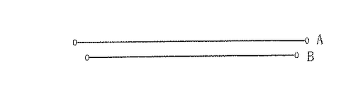
このようなマルチビーム走査光学系においては図28に示すように複数の発光部A,Bを副走査方向に縦に並べて配置してしまうと感光ドラム面上での副走査方向の複数の走査線の間隔が記録密度よりも大幅に間隔が開いてしまう為、通常は図29に示すように複数の発光部A,Bを副走査方向に対応する方向に対して傾けて配置し、その傾け角度δを調整することにより、感光ドラム面上での副走査方向の複数の走査線の間隔を記録密度に合わせて正確に調整している。
【0005】
また感光ドラム面に入射した複数の光束が該感光ドラム面の正反射によってマルチ半導体レーザーに再度戻ってしまうと、該マルチ半導体レーザーの発振が不安定になる為、またはその正反射光が光学系に戻った場合、該光学系の表面反射によって再度感光ドラム面に反射光が戻りゴーストが発生してしまう為に、従来では図30に示すように感光ドラム面97に入射する複数の光束と感光ドラム面97の法線との成す副走査方向の角度が所定の角度(入射角)βを成すように設定している。これにより感光ドラム面97での正反射光が再度マルチ半導体レーザー及び光学系に戻らないような構成をとっている。
【0006】
マルチビーム光走査装置において、このような構成をとった場合、図31に示すように感光ドラム面97上における複数の走査ラインそれぞれの走査倍率が異なってしまうことにより、感光ドラム面97上でのそれぞれのスポットの結像位置に主走査方向のずれが発生してしまい、これが原因となって高画質な画像が得られなくなってくるという問題点があった。
【0007】
この問題点を解決するマルチビーム光走査装置が種々と提案されている(例えば特許文献1,2参照)。特許文献1においては副走査方向の複数光ビームと感光ドラム面の法線とのなす角を所定角度以下に設定することによって、前記主走査方向の結像位置ずれを軽減する構成としている。特許文献2においては主走査方向の結像位置ずれを結像光学系を偏心させて、その偏心量を調節することによって打ち消す構成としている。
【特許文献1】
特開平5−333281号公報
【特許文献2】
特開平9−197308号公報
【0008】
【発明が解決しようとする課題】
しかしながら、これら特許文献で提案されているマルチビーム光走査装置においては、主走査方向の結像位置ずれと結像特性(スポット形状)の両方を同時に満足させることができなかった。
【0009】
例えば特許文献1においては副走査方向の複数光ビームと感光ドラム面の法線とのなす角を所定角度以下に設定することによって主走査方向の結像位置ずれを軽減して目立たなくしようとしているだけであり、主走査方向の結像位置ずれに対する根本的な解決策については何ら開示されていない。
【0010】
また特許文献2においては主走査方向の結像位置ずれを結像光学系を偏心させて、その偏心量を調節することによって打ち消す構成としているが、結像光学系を偏心させて使用すると感光ドラム面における結像スポット形状が劣化しやすいという問題点があり、このため高画質、高記録密度を達成することは難しい。
【0011】
本発明は主走査方向の結像位置ずれと結像特性の両方を同時に満足させ、かつ高速でしかも高画質に最適なマルチビーム光走査装置の提供を目的とする。
【0012】
【課題を解決するための手段】
本発明のマルチビーム光走査装置は、
主走査方向及びそれと垂直な副走査方向の双方で異なる位置に配置された複数の発光部を有する光源手段と、該複数の発光部から各々出射した複数の光束を偏向する反射面を有する回転多面鏡と、該光源手段から該回転多面鏡に至る光路中に配置され、該複数の光束を収束光束又は発散光束に変換する第1の光学系と、該回転多面鏡で偏向された複数の光束を、主走査方向に沿った回転軸を有するドラム状の被走査面上に導光させる第3の光学系と、を有するマルチビーム光走査装置であって、
副走査断面内において、該被走査面に入射する各々の光束は、それらの主光線が該被走査面の法線に対してそれぞれ零でない角度を成すように入射しており、このことによって、該被走査面上の各光束の結像点間に相対的に主走査方向に平行な第1の方向に生じる位置ずれ量の最大値をδY1、主走査方向において収束光束又は発散光束が該第3の光学系に入射することによって、該被走査面上の各光束の結像点間に相対的に主走査方向に平行な第2の方向に生じる位置ずれ量の最大値をδY2、該複数の発光部から出射する光束は相対的な波長差を有し、その相対的な波長差によって被走査面上の各光束の結像点間に相対的に主走査方向に平行な第3の方向に生じる位置ずれ量の最大値をδY3とするとき、
|δY1+δY2+δY3|≦MAX(|δY1|、|δY2|、|δY3|)‥‥(1)
(但しMAX(|δY1|、|δY2|、|δY3|)はδY1、δY2、δY3のうちの絶対値の最も大きい値である。)
を満足することを特徴としている。
【0013】
【発明の実施の形態】
[実施形態1]
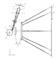
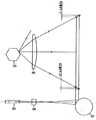
図1は本発明の実施形態1の主走査方向の要部断面図(主走査断面図)、図2は図1の副走査方向の要部断面図(副走査断面図)である。
【0014】
ここで、主走査方向とは回転多面鏡の回転軸及び走査レンズ系の光軸に垂直な方向(回転多面鏡で光束が反射偏向(偏向走査)される方向)を示し、副走査方向とは回転多面鏡の回転軸と平行な方向を示す。また主走査断面とは主走査方向に平行で走査レンズ系の光軸を含む平面を示す。また副走査断面とは主走査断面と垂直な断面を示す。
【0015】
図1、図2において1は光源手段であり、例えば複数の発光部(発光点)A,Bを副走査方向に対応する方向に対して任意の角度傾けて配置したマルチ半導体レーザーより成っている。
【0016】
2は第1の光学系としての集光レンズ(コリメーターレンズ)であり、光源手段1から出射された複数の光束を収束光束(もしくは発散光束)に変換している。
【0017】
4は第2の光学系としてのレンズ系(シリンドリカルレンズ)であり、副走査方向にのみ所定の屈折力を有しており、集光レンズ2を通過した複数の光束を副走査断面内で後述する回転多面鏡(ポリゴンミラー)5の反射面(ポリゴン面)5aにほぼ線像として結像させている。
【0018】
3は開口絞りであり、シリンドリカルレンズ4を通過した複数の光束の光束幅を制限している。
【0019】
5は複数の発光部A,Bから各々出射した複数の光束を偏向する反射面を有する回転多面鏡(ポリゴンミラー)であり、モーター等の駆動手段(不図示)により図中矢印5b方向に一定速度で回転している。
【0020】
6は第3の光学系としてのfθ特性を有するfθレンズ系(走査レンズ系)であり、第1、第2の2枚のfθレンズ(走査レンズ)6a,6bを有している。このfθレンズ系6はポリゴンミラー5で偏向反射された複数の光束を被走査面7に結像させると共に副走査断面内においてポリゴンミラー5の反射面5aと被走査面7との間を略共役関係にすることにより、該反射面5aの倒れを補正している。
【0021】
7は被走査面としての感光ドラム面(像担持体面)であり、主走査方向に沿った回転軸を有するドラム状より成っている。
【0022】
本実施形態において画像情報に応じてマルチ半導体レーザー1から光変調され出射した2つの光束は集光レンズ2によって収束光束に変換され、シリンドリカルレンズ4に入射する。シリンドリカルレンズ4に入射した光束のうち主走査断面内においてはそのままの状態で出射して開口絞り3を通過する(一部遮光される)。また副走査断面内においては収束して開口絞り3を通過し(一部遮光される)ポリゴンミラー5の反射面5aにほぼ線像(主走査方向に長手の線像)として結像する。そしてポリゴンミラー5の反射面5aで反射偏向された2つの光束は各々fθレンズ系6を介して感光ドラム面7上に導光され、該ポリゴンミラー5を図中矢印5b方向に回転させることによって、該感光ドラム面7上を図中矢印7b方向(主走査方向)に等速度で光走査している。これにより記録媒体としての感光ドラム面7上に2本の走査線を形成し、画像記録を行っている。
【0023】
本実施形態においては前述の如く感光ドラム面7からの正反射光が再度光学系に戻らないように、図2に示すように該感光ドラム面7に入射する2つの光束の主光線と感光ドラム面の法線との成す副走査方向の角度が所定の角度(入射角)βを成すように設定している。
【0024】
このような感光ドラム面7に入射する2つの光束の主光線と該感光ドラム面7の法線との成す副走査方向の角度が所定の角度βを成すように設定した場合、それぞれのスポットの結像位置が主走査方向にずれるという問題点が発生する。
【0025】
ここでそれぞれのスポットの結像位置が主走査方向にずれる原理を図22を用いて説明する。尚、説明を簡単にする為に、ここでは発光部の数を2つと仮定して説明する。
【0026】
図22は感光ドラム面7上に2本の走査線が平行して走査される様子を表わした要部斜視図である。同図において主走査方向をY軸とし、副走査方向、即ち感光ドラムが移動する方向をZ軸とし、感光ドラム面7の法線方向をX軸とする直交座標系を考える。
【0027】
同図に示したように最大走査画角のときにおける感光ドラム面7に入射する光束の主光線とfθレンズ系の光軸との成す角をθとし、XY平面と感光ドラム面7に入射する光束が形成する平面との成す角度をβとする。
【0028】
このとき2本の走査線は光束の進行方向に光路長差δLが発生し、その光路長差δLは感光ドラム面7上を同時に走査される各走査線の副走査方向の間隔をPとするとき
δL=P×sinβ
で表わすことができる。
【0029】
さらに上記光束の進行方向の光路長差δLが発生することにより、感光ドラム面7に入射する2つの光束の主光線は主走査方向(Y方向)にも位置ずれが発生してしまい、その位置ずれ量δY1(最大値)は同図のY方向の端部において、
δY1=δL×tanθ=P×sinβ×tanθ
で表わすことができる。
【0030】
同図において、Z方向のプラス側(上側)の走査線に対するZ方向のマイナス側(下側)の走査線の位置ずれの方向がY方向のプラス側であるとき、δY1の符号を+とする。
【0031】
本実施形態は上記位置ずれ量δY1がプラスの場合、fθレンズ系6に入射させる光束を収束光束とすることによって生じる感光ドラム面7上におけるそれぞれの光束の結像点の主走査方向の位置ずれ量δY2がマイナスになり、さらに2つの発光部A,Bから出射する光束の相対的な波長差によって発生する倍率色収差による感光ドラム面7上の各光束の結像点間の主走査方向の位置ずれ量δY3がマイナスになるようにし、上記位置ずれ量δY1と、位置ずれ量δY2と位置ずれ量δY3を加算した量が互いに相殺方向となるように、感光ドラム面7に入射するそれぞれの光束と該感光ドラム面7の法線との副走査方向の入射角、主走査断面内における最大走査画角のときにおける感光ドラムに入射する光束の主光線と感光ドラム面7の法線とのなす角度θ、fθレンズ系6に入射させる光束の収束度合い等を設定するものである。
【0032】
また上記位置ずれ量δY1がマイナスの場合、上記位置ずれ量δY2をプラスとし、さらに上記位置ずれ量δY3がプラスになるようにし、上記位置ずれ量δY1と、位置ずれ量δY2と位置ずれ量δY3とを加算した量が互いに相殺方向となるように、感光ドラム面7に入射するそれぞれの光束と該感光ドラム面7の法線との副走査方向の入射角β、主走査断面内における最大走査画角のときにおける感光ドラム面7に入射する光束の主光線と該感光ドラム面7の法線とのなす角度θ、fθレンズ系6に入射させる光束の収束度合い等々を設定するものである。
【0033】
以下、図を用いてfθレンズ系6に入射させるそれぞれの光束を収束光束とした場合に、感光ドラム面7上におけるそれぞれの光束の結像点に主走査方向の位置ずれが発生する原理を説明する。尚、説明を簡単にする為に前述と同様、発光部の数を2つと仮定して説明する。
【0034】
前述の如く図29に示すように2つの発光部A,Bを副走査方向に対応する方向に対して傾けて配置する構成のマルチビーム光走査装置においては、2つの光束がポリゴンミラー5で偏向反射された後の反射角がそれぞれ異なる為に感光ドラム面7上においては互いに主走査方向に離れた位置にスポットが結像されてしまう。よってこのような構成のマルチビーム光走査装置においては、ある1つの基準の発光部から出射した光束が感光ドラム面7上に結像する位置に、もう一方の発光部から出射した光束の結像位置を合わせるように所定時間δTだけタイミングをずらして画像データを送っている。
【0035】
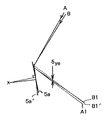
この様子を示したのが図23である。図23は走査開始側における2つの光束の主光線がポリゴンミラー5の反射面(ポリゴン面)5aで反射される様子を示した説明図である。
【0036】
同図において最初に発光部Aから出射された光束がポリゴンミラー5の反射面5aで反射されて図中A1の方向に反射され、fθレンズ系(不図示)6により感光ドラム面7上に結像される。
【0037】
次に所定時間δTだけ時間がずれたときの反射面5a´によって発光部Bから出射された光束が反射され、図中B1´の方向、即ち図中A1と同じ方向に反射されることによって互いのスポットの結像位置が一致することになる。
【0038】
但し、ポリゴンミラー5で反射された後の2つの光束の主光線はfθレンズ系6に入射する角度は等しいものの、それぞれの光束の主光線の反射位置にずれが生じる為に主走査方向にδysだけずれてfθレンズ系6に入射することになる。
【0039】
fθレンズ系6に入射する2つの光束が略平行光束の場合には、それぞれの光束の主光線に主走査方向にδysだけずれが生じても感光ドラム面7上におけるスポットの結像位置は同じである。
【0040】
しかしながらfθレンズ系6に入射する2つの光束が収束光束の場合には、それぞれの光束の主光線に主走査方向にδysだけずれが生じると感光ドラム面7上におけるスポットの主走査方向の結像位置にもずれが生じる。
【0041】
図25はこの現象を説明する為の光学系の要部概略図である。同図において6はfθレンズ系であり、fθレンズ系6の光出射側主平面11からfθレンズ系6に入射する収束光束の自然収束点14までの距離をSd、fθレンズ系6の焦点距離をf、fθレンズ系6の光出射側主平面11からfθレンズ系6に入射した収束光束がfθレンズ系6によって収束されて結像される位置(即ち、ここが感光ドラム面となる)12までの距離をSkとする。
【0042】
ここにおいて、
【0043】
【数1】

であるから、
【0045】
【数2】
で表わされる。
【0047】
また各発光部A、Bから出射した各々の光束の主光線の主走査方向のずれ量をδy、各発光部A、Bから出射した各々の光束の感光ドラム面7上における主走査方向のスポットの結像位置のずれ量をδY2(最大値)とすれば、同図から明らかに、
【0048】
【数3】
だけ、ずれが発生することになる。
【0050】
図24は走査終了側における2つの光束の主光線がポリゴンミラー5の反射面で偏向反射される様子を示した説明図である。
【0051】
同図において最初に発光部Aから出射された光束がポリゴンミラー5の反射面5aで反射されて図中A1の方向に反射され、fθレンズ系(不図示)6により感光ドラム面7上に結像される。
【0052】
次に所定時間δTだけ時間がずれたときの反射面5a´によって発光部Bから出射された光束が反射され、図中B1´の方向、即ち図中A1と同じ方向に反射され、このときそれぞれの光束の主光線は主走査方向にδyeだけずれてfθレンズ系6に入射する。
【0053】
図23、図24から分かるように走査開始側及び走査終了側ともに発光部Aから出射した光束A´よりも発光部Bから出射した光束B´の方がfθレンズ系6の光軸側にずれている為、感光ドラム面7上では図26に示すように光束A´で走査したライン(走査線)よりも光束B´で走査したラインの方が短くなる。
【0054】
即ち、fθレンズ系6に入射させる2つの光束を収束光束とした場合には、感光ドラム面7上におけるそれぞれの光束の結像点に主走査方向の位置ずれ量δY2が発生することになる。
【0055】
一方、複数の発光部を有する半導体レーザーの個々の発光部から出射する光束に、相対的な波長差が存在する場合、よく知られているようにfθレンズ系によって倍率色収差が発生する。その結果、相対的な波長差によって被走査面上のそれぞれの光束の結像点に主走査方向の位置ずれ量δY3が発生することになる。
【0056】
本実施形態では副走査断面内において、感光ドラム面7に入射する各々の光束は、それらの主光線が該感光ドラム面7の法線に対してそれぞれ零でない角度を成すように入射しており、このことによって、該感光ドラム面7上の各光束の結像点間に相対的に主走査方向に平行な第1の方向に生じる位置ずれ量の最大値をδY1、主走査方向において収束光束又は発散光束がfθレンズ系6に入射することによって、該感光ドラム面7上の各光束の結像点間に相対的に主走査方向に平行な第2の方向に生じる位置ずれ量の最大値をδY2、2つの発光部A,Bから出射する光束は相対的な波長差を有し、その相対的な波長差によって感光ドラム面7上の各光束の結像点間に相対的に主走査方向に平行な第3の方向に生じる位置ずれ量の最大値をδY3とするとき、
|δY1+δY2+δY3|≦MAX(|δY1|、|δY2|、|δY3|)‥‥(1)
(但しMAX(|δY1|、|δY2|、|δY3|)はδY1、δY2、δY3のうちの絶対値の最も大きい値である。)
を満足させている。
【0057】
即ち、本実施形態においては上記の条件式(1)を満たすようにトータルの位置ずれ量が、位置ずれ量δY1、δY2、δY3のうちの絶対値の最も大きい値より小さい又は等しく成るように、さらに位置ずれ量δY1と、位置ずれ量δY2と位置ずれ量δY3とを加算した量が、互いに逆の方向にずれて相殺される方向になるように、上記入射角β、及びfθレンズ系6の光出射側主平面からfθレンズ系6に入射する収束光束の自然収束点までの距離Sd、fθレンズ系6の光出射側主平面からfθレンズ系6に入射した収束光束がfθレンズ系6によって収束されて結像される位置までの距離Sk等、を最適に選択に設定することにより、感光ドラム等からなる被走査面全域において複数のスポットの主走査方向の結像位置のずれを効果的に補正している。
【0058】
ところで画像形成装置内部の構成によっては感光ドラム面7に入射する2つの光束と該感光ドラム面7の法線との副走査方向の所定の入射角βを任意に設定することができない場合も有り得る。そのような場合においては2つのスポットの主走査方向の結像位置のずれをほぼ完全に補正することは難しいので画像上許容出来る程度にまで補正してやれば良い。
【0059】
一般に主走査方向の結像点の位置ずれは、14μm(0.014mm)を超えたところから視認されやすくなり、画像に対する影響が無視できないものとなる。
【0060】
従って位置ずれ量δY1、δY2、δY3を各々mm単位で表わしたとき、
|δY1+δY2+δY3|≦0.014(mm) ‥‥(2)
を満足することが好ましい。
【0061】
ここで上記fθレンズ系6に入射させる2つの光束を収束光束とした場合に生じるそれぞれのスポットの結像位置の主走査方向のずれ量δY2は、fθレンズ系6の光出射側主平面からfθレンズ系6に入射する収束光束の自然収束点までの距離Sd、fθレンズ系6の光出射側主平面からfθレンズ系6に入射した収束光がfθレンズ系6によって収束されて結像される位置までの距離Skの比を非平行度K=Sk/Sdとすると、Kの値が大きければ大きい程、即ち、非平行度が強ければ強い程上記ずれ量δY2の値を大きくすることが出来、ずれ量δY1と相殺しやすくすることが可能となる。
【0062】
しかしながら、非平行度Kをあまり強くし過ぎると、ポリゴンミラー5の回転中心と各ポリゴン面までの距離の誤差によって発生する、ポリゴン面数周期のジッターが増大してしまう為、本実施形態においては、感光ドラム面7に入射する2つの光束と該感光ドラム面7の法線とが副走査方向に所定の入射角βをなして配置した場合に生じるそれぞれのスポットの結像位置の主走査方向の位置ずれ量δY1を、fθレンズ系6に入射させる複数の光束を収束光束とした場合に生じるそれぞれのスポットの結像位置の主走査方向の位置ずれ量δY2のみで相殺するのではなく、上記位置ずれ量δY2と、2つの発光部から出射する光束の相対的な波長差によって発生する倍率色収差によって生じるそれぞれのスポットの結像位置の主走査方向の位置ずれ量δY3とを加算した量とで上記位置ずれ量δY1を相殺する構成としている。
【0063】
そうすることによって、ポリゴンミラー5の回転中心と各反射面までの距離の誤差によって発生する、ポリゴン面数周期のジッター量を小さく設定している。
【0064】
即ち、上記位置ずれ量δY1と、位置ずれ量δY2と位置ずれ量δY3は
δY1×(δY2+δY3)<0 ‥‥(3)
を満足させることが好ましい。
【0065】
以上の説明は、理解を簡単にする為に発光部の数を2つと仮定して説明してきたが、本実施形態においては発光部の数を2つに限定するものではなく、むしろ発光部の数が多数の場合に、より一層の効果を得ることが出来ることは容易に想像がつくであろう。
【0066】
表−1、表−2に本発明の実施形態1のマルチビーム光走査装置の諸特性を示す。
【0067】
【表1】
【表2】
ここでfθレンズ系6の主走査断面の非球面形状は、各レンズ面と光軸との交点を原点とし、光軸方向をX軸、主走査断面内において光軸と直交する軸をY軸、副走査断面内において光軸と直交する軸をZ軸としたときに、
【0070】
【数4】
なる非球面式で表わされる。
【0072】
なお、Rは曲率半径、k、B4〜B10は非球面係数である。
【0073】
一方副走査断面の形状は主走査方向のレンズ面座標がyであるところの主走査面の法線方向の曲率半径r′が、
【0074】
【数5】
なる式で表わされる形状をしている。
【0076】
なお、rは光軸上における曲率半径、D2〜D10は各係数である。
【0077】
ここで各係数がyの値の正負によって異なる場合は、yの値が正のときは係数として添字uのついたD2u〜D10uを用いて計算された曲率半径r’となっており、yの値が負のときは係数として添字lのついたD2l〜D10lを用いて計算された曲率半径r’となっている。
【0078】
本実施形態のマルチビーム光走査装置においては図1に示すように2つの発光部A,Bを配置しており、2つの発光部A,Bの間隔dは0.1mmである。副走査断面内では、発光部Aが上側、発光部Bが下側に配置されており、それぞれの発光部A,Bから出射した光束は、集光レンズ2、シリンドリカルレンズ4を通って、ポリゴンミラー5の反射面5a上に主走査方向に細長い線状に結像される。
【0079】
図2に示すようにポリゴンミラー5の反射面5a上では、発光部Aから出射した光束は下側、発光部Bから出射した光束は上側に結像され、その後ポリゴンミラー5の反射面5aで反射された光束はfθレンズ系6により感光ドラム面7上にスポット状に結像される。感光ドラム面7上では、発光部Aから出射した光束は上側、発光部Bから出射した光束は下側に結像されることとなる。
【0080】
図2において、感光ドラム面7の法線と、各発光部A、Bからの光束は、それぞれ副走査方向に角度βを成すように配置されている。ここで図22を参照すれば2つの光束と感光ドラムが配置されている場合には同図の上側の光束で走査したラインの方が長くなることになる。
【0081】
本実施形態においては、図2に示すように副走査方向の角度βを設定している為、図3に示すように各発光部A,Bから出射した光束の感光ドラム面7上での結像位置ずれが発生することによって、発光部Aからの光束で走査したラインが短く、発光部Bからの光束で走査したラインが長くなることは容易に理解できるであろう。
【0082】
上記位置ずれを、以下、第1の位置ずれと称する。
【0083】
一方、図23、図24で説明したように、発光部A、Bが、本実施形態の図1の如く配置されている場合には、集光レンズ2から出射した光束を収束光束とした場合、図4に示すように発光部Aからの光束で走査したラインが長く、発光部Bからの光束で走査したラインが短くなることになる。
【0084】
上記位置ずれを、以下、第2の位置ずれと称する。
【0085】
また2つの発光部A、Bから出射した光束に相対的な波長差が存在する場合には、良く知られているように倍率色収差が発生する。一般の光学硝子及び光学用のプラスチック材料の屈折率の波長依存性は、波長が長くなれば屈折率が低くなる特性を有している。そこで本実施形態においては、発光部Bから出射する光束の波長を、基準波長である780nmに設定し、発光部Aから出射する光束の波長を、基準波長に対して2nm長い782nmに設定してある。この場合、図5で示すように発光部Aからの光束で走査したラインが長く、発光部Bからの光束で走査したラインが短くなることになる。
【0086】
上記位置ずれを、以下、第3の位置ずれと称する。
【0087】
本実施形態では上記の如く第1、第2、第3の位置ずれの量δY1、δY2、δY3が条件式(1)を満たすように設定されており、さらに第2、第3の位置ずれが該第1の位置ずれの方向に対して反対方向に設定されており、該第2の位置ずれと第3の位置ずれを加算した量が、ほぼ第1の位置ずれの量と等しくなって相殺される方向に設定されており、最終的に図6に示すように発光部Aからの光束で走査したラインと発光部Bからの光束で走査したラインの長さを実質的に等しくすることを可能としている。
【0088】
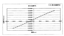
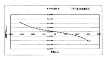
本実施形態における第1の位置ずれ量δY1を図7に示す。同図において横軸は像高であり、縦軸は位置ずれ量をmm単位でプロットしてあり、発光部Aから出射した光束の結像位置に対して、発光部Bから出射した光束の結像位置がどれだけ位置ずれしているかをプロットしたものである。
【0089】
本実施形態において発光部Aから出射した光束の結像位置に対して、発光部Bから出射した光束の結像位置が図22における座標系でY方向にプラス方向にずれているときを縦軸のプラス方向にとっている。ここで本実施形態においては図2における副走査方向の角度βは20度に設定されている。
【0090】
図7における横軸を、主走査面内におけるfθレンズ系6によって感光ドラム面7上を走査される光束と該感光ドラム面7の法線とのなす角度θにとってプロットしたものが図8である。本実施形態においては角度θの最大値θmaxは29.306度に設定されている。
【0091】
次に本実施形態における第2の位置ずれ量δY2を図9に示す。同図において横軸、縦軸の設定は図7と同様である。
【0092】
本実施形態においてはfθレンズ系6の光出射側主平面から1034.45644mmの位置に集光するような収束光束を該fθレンズ系6に入射させており、その光束を該fθレンズ系6によって、該fθレンズ系6の光出射側主平面から202.92744mmの位置に結像させており、非平行度Kは、K=Sk/Sd=0.19617に設定されている。また集光レンズ2の焦点距離fは30.55254mmであり、2つの発光部A,Bの間隔dは0.1mmであるので、集光レンズ2から出射した2つの光束の主光線の主走査断面内における相対角度差αは0.18753度である。
【0093】
また本実施形態における第3の位置ずれ量δY3を図10に示す。同図において横軸、縦軸の設定は図7と同様である。
【0094】
本実施形態においては発光部Bから出射する光束の波長を、基準波長である780nmに設定し、発光部Aから出射する光束の波長を、基準波長に対して2nm長い782nmに設定してある。
【0095】
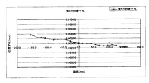
上記第1、第2、第3のずれ量δY1,δY2,δY3を合計したものが実際に残存するずれ量のトータルとなり、その量を図11に示す。図11から分かるように感光ドラム面7に入射するそれぞれの光束と該感光ドラム面7の法線とが副走査方向に所定の入射角βをなして配置した場合に発生する第1の位置ずれ量δY1と、fθレンズ系6に収束光束を入射させることによって発生する第2の位置ずれ量δY2と、各光束の相対的な波長差によって発生する第3の位置ずれ量δY3とで効果的に補正できていることが理解できる
本実施形態においては最終的なトータルの位置ずれ量が、位置ずれ量δY1、δY2、δY3のうちの絶対値の最も大きい値より小さい又は等しく成るように抑えられており、前記条件式(1)を満足していることがわかる。また最終的なトータルの位置ずれ量が有効走査領域全域において、3μm(0.003mm)以下という小さな量に抑えられており、前記条件式(2)を満足していることがわかる。また第1の位置ずれの方向と、第2、第3の位置ずれの方向は逆方向であるから、前記条件式(3)をも満足していることがわかる。
【0096】
このように本実施形態においては上記の如く条件式(1)を満足するように、さらに条件式(2)又は/及び条件式(3)をも満足するように、集光レンズ2から出射した2つの光束の主光線の主走査断面内における相対角度差α、副走査方向における感光ドラムに入射する2つの光束の主光線が感光ドラム面7の法線に対して成す角の平均値β、主走査断面内におけるfθレンズ系6によって感光ドラム面7上を走査される2つの光束の最大走査位置における感光ドラム面7の法線と2つの光束とのなす角度θ、2つの発光部A,Bから出射した2つの光束の相対的な波長差δλ、集光レンズ2によって収束光束(又は発散光束)に変換された2つの光束の非平行度Kをそれぞれ最適に設定している。
【0097】
それによって主走査方向の結像位置ずれを効果的に補正し、高速でしかも高画質に最適なマルチビーム光走査装置を実現することを可能としている。
【0098】
[実施形態2]
次に本発明の実施形態2について説明する。
【0099】
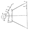
図12は本発明の実施形態2の主走査方向の要部断面図(主走査断面図)、図13は図12の副走査方向の要部断面図(副走査断面図)である。図12、図13において図1、図2に示した要素と同一要素には同符番を付している。
【0100】
本実施形態において前述の実施形態1と異なる点は、
(1)発光部の数Nを2つから4つ(発光部A,B,C,D)に変更した点、
(2)副走査断面内における複数の光束と感光ドラム面7の法線とのなす角度βを20度から14.1度に変更した点、
(3)発光部Dから出射する光束の波長を、基準波長である780nmに設定し、発光部Aから出射する光束の波長を、基準波長に対して5nm長い785nmに設定した点、
である。その他の構成及び光学的作用は実施形態1と略同様であり、これにより同様な効果を得ている。
【0101】
即ち、本実施形態において発光部の数Nが増加するにしたがって、前述した第1のずれ量δY1が増大することは容易に理解できるであろう。本実施形態は発光部の数Nが増加すればする程より一層の効果を発揮するものである。
【0102】
ここで発光部A,Bは光源ユニットLH1を構成し、発光部C,Dは光源ユニットLH2を構成している。2つの光源ユニットLH1、LH1は光源手段の一部を構成している。
【0103】
図14に本実施形態における第1の位置ずれ量δY1を示す。同図において横軸は像高であり、縦軸は位置ずれ量をmm単位でプロットしてあり、発光部Aから出射した光束の結像位置に対して、発光部Dから出射した光束の結像位置がどれだけ位置ずれしているかをプロットしたものである。
【0104】
本実施形態において発光部Aから出射した光束の結像位置に対して、発光部Dから出射した光束の結像位置が図22における座標系でY方向にプラス方向にずれているときを縦軸のプラス方向にとっている。図7と比較して明らかに位置ずれ量が増大していることが分かる。本実施形態においては図13における副走査方向の角度βを14.1度に設定している。
【0105】
図14における横軸を、主走査面内におけるfθレンズ系6によって感光ドラム面7上を走査される光束と該感光ドラム面7の法線とのなす角度θにとってプロットしたものが図15である。本実施形態においても角度の最大値θmaxは実施形態1と同様29.306度に設定されている。
【0106】
次に本実施形態における第2の位置ずれ量δY2を図16に示す。同図において横軸、縦軸の設定は図14と同様である。
【0107】
本実施形態においては実施形態1と同様、fθレンズ系6の光出射側主平面から1034.45644mmの位置に集光するような収束光束をfθレンズ系6に入射させており、その光束を該fθレンズ系6によって、該fθレンズ系6の光出射側主平面から202.92744mmの位置に結像させており、非平行度Kは、K=Sk/Sd=0.19617に設定されている。また集光レンズ2の焦点距離fcolは30.55254mmであり、4つの発光部A,B,C,Dの各間隔dは0.1mmであるので、集光レンズ2から出射した4つの光束の主光線の主走査断面内における相対角度差の最大値αは0.56259度である。
【0108】
また本実施形態における第3の位置ずれ量δY3を図17に示す。同図において横軸、縦軸の設定は図14と同様である。
【0109】
本実施形態においては発光部Dから出射する光束の波長を、基準波長である780nmに設定し、発光部Aから出射する光束の波長を、基準波長に対して5nm長い785nmに設定してある。
【0110】
上記第1、第2、第3のずれ量δY1、δY2、δY3を合計したものが実際に残存するずれ量のトータルとなり、その量を図18に示す。図18から分かるように感光ドラム面7に入射するそれぞれの光束と該感光ドラム面7の法線とが副走査方向に所定の入射角βをなして配置した場合に発生する第1の位置ずれ量δY1と、fθレンズ系6に収束光束を入射させることによって発生する第2の位置ずれ量δY2と、各光束の相対的な波長差によって発生する第3の位置ずれ量δY3で効果的に補正できていることが理解できる。
【0111】
本実施形態においては最終的なトータルの位置ずれ量が、位置ずれ量δY1、δY2、δY3のうちの絶対値の最も大きい値より小さい又は等しく成るように抑えられており、前記条件式(1)を満足していることがわかる。また最終的なトータルの位置ずれ量が、有効走査領域全域において、約5μm(0.005mm)以下という小さな量に抑えられており、前記条件式(2)を満足していることがわかる。また第1の位置ずれの方向と、前記第2、第3の位置ずれの方向は逆方向であるから、前記条件式(3)をも満足していることがわかる。
【0112】
また本実施形態においては、
・発光部の数Nは4、
・集光レンズ2から出射した4つの光束の主光線と、fθレンズ系6の光軸とのなす角度の平均値γは70度、
・集光レンズ2の焦点距離fcolは30.55254mm、
・4つの発光部A,B,C,Dの間隔dは0.1mm、
・副走査断面内における、感光ドラム面7に入射する4つの光束の主光線が該感光ドラム面7の法線に対して成す角の平均値βは14.1度、
・ポリゴンミラーの内接円半径rは17.32051mm、
・ポリゴンミラーによって偏向走査される4つの光束の最大走査角度ηは41.75084度、
・主走査断面内における、fθレンズ系6によって感光ドラム面7上を走査される4つの光束の最大走査位置における該感光ドラム面7の法線と4つの光束とのなす角度θmaxは29.306度、
・4つの発光部A,B,C,Dから出射した4つの光束の相対的な波長差の最大値をδλは5nm、
・fθレンズ系6の光出射側主平面から集光レンズ2によって変換された収束光束又は発散光束の自然集束点までの距離Sdは1034.45644mm、
・fθレンズ系6の光出射側主平面から集光レンズ2によって変換された収束光束又は発散光束がfθレンズ系6によって収束されて結像される位置までの距離Skは202.92744mm
・fθレンズ系6のfθ係数fは212.71058mm
・解像度から決定される4つの光束の感光ドラム面7上における副走査方向の結像点の間隔Pは0.042333mm(600DPIである)、
となるように、各パラメータを設定している。
【0113】
ここで感光ドラム面7に入射するそれぞれの光束と該感光ドラム面7の法線とが副走査方向に所定の入射角βをなして配置した場合に発生する、発光部Aから出射した光束の結像位置と発光部Dから出射した光束の結像位置とのずれ量である第1のずれ量δY1は、
【0114】
【数6】
で表すことができる。
【0116】
一方、fθレンズ系6に収束光束を入射させることによって発生する第2の位置ずれ量δY2は、図23と図24を参照すれば、図23におけるδysよりも図24におけるδyeの方が大きい為、第2の位置ずれ量δY2は反光源手段1側の最大走査位置において最大となる。
【0117】
ここで、上記第2の位置ずれ量δY2は、
【0118】
【数7】
と近似することが出来る。
【0120】
また4つの発光部A,B,C,Dから出射した光束に相対的な波長差が存在する場合の倍率色収差による第3の位置ずれ量δY3は、fθレンズ系6を構成する光学硝子、或いは光学用プラスチック材料の分散値に設定される。通常の光学硝子、光学用プラスチック材料の分散値の範囲においては、第3の位置ずれ量δY3は、
δY3=9.5δλf
で近似することができる。
【0121】
ここにおいて、図14又は図15及び図16、図17から分かるように本実施形態においては、第1のずれ量δY1を、反対方向の第2、第3のずれ量δY2、δY3で補正する構成となっており、その補正残差δallは、近似的に第1、第2、第3のずれ量δY1、δY2、δY3を用いて、
【0122】
【数8】
と書き表すことが出来る。
【0124】
一般に、主走査方向の結像点の位置ずれは、14μm(0.014mm)を超えたところから視認されやすくなり、画像に対する影響が無視出来ないものとなる為、
【0125】
【数9】
を満足することが望ましい。
【0127】
本実施形態における各数値を(4)式に代入すると、
δall=0.00277
となり、これは条件式(4)を満足している。
【0128】
このように本実施形態においては、上記条件式(4)を満足させるように、光学系の各諸元を設定することによって、主走査方向の結像位置ずれを効果的に補正し、高速でしかも高画質に最適なマルチビーム光走査装置を実現することを可能としている。
【0129】
[実施形態3]
次に本発明の実施形態3について説明する。
【0130】
図19は本発明の実施形態3の主走査方向の要部断面図(主走査断面図)、図20は図19の副走査方向の要部断面図(副走査断面図)である。図19、図20において図1、図2に示した要素と同一要素には同符番を付している。
【0131】
本実施形態において前述の実施形態1と異なる点は、
(1)1つの発光部A・Bを有する光源1・1が2つであり、それぞれの光源1・1に対応した集光レンズ2・2も2つであることである。その他の構成及び光学的作用は実施形態1と略同様であり、これにより同様な効果を得ている。
【0132】
ここにおいて、ポリゴンミラー5に入射する2つの光束の主光線の主走査断面内における相対角度差の最大値αは4度に設定されている。またfθレンズ系6の光出射側主平面から3316.80933mmの位置に集光するような収束光束をfθレンズ系6に入射させており、その光束を該fθレンズ系6によって、該fθレンズ系6の光出射側主平面から201.05427mmの位置に結像させており、非平行度Kは、K=Sk/Sd=0.06062に設定されている。また2つの発光部A,Bから出射した光束の相対的な波長差はゼロとしており、その他の諸元は実施形態2と同様に設定されている。
【0133】
図23及び図24を参照すれば、発光部Aからの光束と発光部Bからの光束との成す角が大きくなればなる程、δys及びδyeの量が大きくなることは容易に理解できる。即ち、ポリゴンミラー5に入射する2つの光束の主光線の主走査断面内における相対角度差の最大値αを大きくすればするほど、fθレンズ系6に収束光束を入射させることによって発生する第2の位置ずれ量δY2を大きくすることが分かる。
【0134】
この原理を利用すれば、感光ドラム面7に入射するそれぞれの光束と該感光ドラム面7の法線とが副走査方向に所定の入射角βをなして配置した場合に発生する、発光部Aから出射した光束の結像位置と発光部Bから出射した光束の結像位置のずれ量である第1のずれ量δY1を、2つの発光部A,Bの相対的波長差による第3のずれ量δY3を使用しないで、第2のずれ量δY2のみで補正することが可能となる。
【0135】
本実施形態においては、上記角度αを4度と大きく設定することにより、感光ドラム面7に入射するそれぞれの光束と該感光ドラム面7の法線とが副走査方向に所定の入射角βをなして配置した場合に発生する、発光部Aから出射した光束の結像位置と発光部Dから出射した光束の結像位置とのずれ量である第1のずれ量δY1を、fθレンズ系6に収束光束を入射させることによって発生する第2の位置ずれ量δY2のみで補正を行っていることに特徴がある。
【0136】
ここにおいて、前記第1のずれ量δY1は、実施形態2で説明した式、
【0137】
【数10】
![]()
で計算することができる。
【0139】
一方、前記第2のずれ量δY2は、
【0140】
【数11】
と近似することができる。
【0142】
本実施形態においては、上記第1のずれ量δY1をずれ量δY2のみで補正を行っている為、その補正残差δallは、近似的に、上記第1、第2のずれ量δY1、δY2を用いて、
【0143】
【数12】
と書き表すことが出来る。
【0145】
一般に主走査方向の結像点の位置ずれは、14μm(0.014mm)を超えたところから視認されやすくなり、画像に対する影響が無視できないものとなる為、
【0146】
【数13】
を満足することが望ましい。
【0148】
本実施形態における各数値を条件式(5)に代入すると、
δall=0.00464
となり、これは条件式(5)を満足している。
【0149】
本実施形態においては、上記条件式(5)を満足させるように、光学系の各諸元を設定することによって主走査方向の結像位置ずれを効果的に補正し、高速でしかも高画質に最適なマルチビーム光走査装置を実現することを可能としている。
【0150】
ここで本実施形態において感光ドラム面7に入射するそれぞれの光束と該感光ドラム面7の法線が副走査方向に所定の入射角βをなして配置した場合に発生する、発光部Aから出射した光束の結像位置と発光部Bから出射した光束の結像位置のずれ量である第1のずれ量δY1を、2つの発光部A,Bの相対的波長差による第3のずれ量δY3を使用しないで、第2のずれ量δY2のみで補正したが、もちろん、2つの発光部A,Bの相対的波長差による第3のずれ量δY3を補正に使用しても本発明の趣旨を逸脱することにはならない。
【0151】
その場合、前記条件式(5)に代わり、
【0152】
【数14】
を満足すれば良いことになる。
【0154】
このように本実施形態においては、上記条件式(5)又は条件式(6)を満足させるように、光学系の各諸元を設定することによって、主走査方向の結像位置ずれを効果的に補正し、高速でしかも高画質に最適なマルチビーム光走査装置を実現することを可能としている。
【0155】
尚、本発明の各実施形態においては、集光レンズ2から出射する光束を収束光束として説明してきたが、発散光束としても同様な補正が可能となることは言うまでもない。その場合、発光部A、発光部B等の2つの発光部A,Bの副走査方向の上下位置を反転することによって同様の補正が可能となることは容易に理解出来るであろう。
【0156】
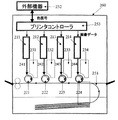
[画像形成装置]
図21は、本発明の画像形成装置の実施形態を示す副走査方向の要部断面図である。図において、符号104は画像形成装置を示す。この画像形成装置104には、パーソナルコンピュータ等の外部機器117からコードデータDcが入力する。このコードデータDcは、装置内のプリンタコントローラ111によって、画像データ(ドットデータ)Diに変換される。この画像データDiは、実施形態1〜4に示した構成を有する光走査ユニット(マルチビーム光走査装置)100に入力される。そして、この光走査ユニット100からは、画像データDiに応じて変調された光ビーム103が出射され、この光ビーム103によって感光ドラム101の感光面が主走査方向に走査される。
【0157】
静電潜像担持体(感光体)たる感光ドラム101は、モータ115によって時計廻りに回転させられる。そして、この回転に伴って、感光ドラム101の感光面が光ビーム103に対して、主走査方向と直交する副走査方向に移動する。感光ドラム101の上方には、感光ドラム101の表面を一様に帯電せしめる帯電ローラ102が表面に当接するように設けられている。そして、帯電ローラ102によって帯電された感光ドラム101の表面に、前記光走査ユニット100によって走査される光ビーム103が照射されるようになっている。
【0158】
先に説明したように、光ビーム103は、画像データDiに基づいて変調されており、この光ビーム103を照射することによって感光ドラム101の表面に静電潜像を形成せしめる。この静電潜像は、上記光ビーム103の照射位置よりもさらに感光ドラム101の回転方向の下流側で感光ドラム101に当接するように配設された現像器107によってトナー像として現像される。
【0159】
現像器107によって現像されたトナー像は、感光ドラム101の下方で、感光ドラム101に対向するように配設された転写ローラ108によって被転写材たる用紙112上に転写される。用紙112は感光ドラム101の前方(図21において右側)の用紙カセット109内に収納されているが、手差しでも給紙が可能である。用紙カセット109端部には、給紙ローラ110が配設されており、用紙カセット109内の用紙112を搬送路へ送り込む。
【0160】
以上のようにして、未定着トナー像を転写された用紙112はさらに感光ドラム101後方(図21において左側)の定着器へと搬送される。定着器は内部に定着ヒータ(図示せず)を有する定着ローラ113とこの定着ローラ113に圧接するように配設された加圧ローラ114とで構成されており、転写部から搬送されてきた用紙112を定着ローラ113と加圧ローラ114の圧接部にて加圧しながら加熱することにより用紙112上の未定着トナー像を定着せしめる。更に定着ローラ113の後方には排紙ローラ116が配設されており、定着された用紙112を画像形成装置の外に排出せしめる。
【0161】
図21においては図示していないが、プリントコントローラ111は、先に説明したデータの変換だけでなく、モータ115を始め画像形成装置内の各部や、後述する光走査ユニット内のポリゴンモータなどの制御を行う。
【0162】
[カラー画像形成装置]
図32は本発明の実施態様のカラー画像形成装置の要部概略図である。本実施形態は、光走査装置を4個並べ各々並行して像担持体である感光ドラム面上に画像情報を記録するタンデムタイプのカラー画像形成装置である。図32において、260はカラー画像形成装置、211,212,213,214は各々実施形態1〜3に示したいずれかの構成を有する光走査装置(マルチビーム光走査装置)、221,222,223,224は各々像担持体としての感光ドラム、231,232,233,234は各々現像器、251は搬送ベルトである。
【0163】
図32において、カラー画像形成装置260には、パーソナルコンピュータ等の外部機器252からR(レッド)、G(グリーン)、B(ブルー)の各色信号が入力する。これらの色信号は、装置内のプリンタコントローラ253によって、C(シアン),M(マゼンタ),Y(イエロー)、B(ブラック)の各画像データ(ドットデータ)に変換される。これらの画像データは、それぞれ光走査装置211,212,213,214に入力される。そして、これらの光走査装置からは、各画像データに応じて変調された光ビーム(マルチビームレーザ−)241,242,243,244が出射され、これらの光ビームによって感光ドラム221,222,223,224の感光面が主走査方向に走査される。
【0164】
本実施態様におけるカラー画像形成装置は光走査装置(211,212,213,214)を4個並べ、各々がC(シアン),M(マゼンタ),Y(イエロー)、B(ブラック)の各色に対応し、各々平行して感光ドラム221,222,223,224面上に画像信号(画像情報)を記録し、カラー画像を高速に印字するものである。
【0165】
本実施態様におけるカラー画像形成装置は上述の如く4つの光走査装置211,212,213,214により各々の画像データに基づいた光ビームを用いて各色の潜像を各々対応する感光ドラム221,222,223,224面上に形成している。その後、記録材に多重転写して1枚のフルカラー画像を形成している。
【0166】
前記外部機器252としては、例えばCCDセンサを備えたカラー画像読取装置が用いられても良い。この場合には、このカラー画像読取装置と、カラー画像形成装置260とで、カラーデジタル複写機が構成される。
【0167】
[本発明の実施態様]
本発明の様々な例と実施形態が示され説明されたが、当業者であれば、本発明の趣旨と範囲は本明細書内の特定の説明と図に限定されるのではなく、本願特許請求の範囲に全て述べられた様々の修正と変更に及ぶことが理解されるであろう。
【0168】
本発明の実施態様の例を以下に列挙する。
【0169】
[実施態様1]
主走査方向及びそれと垂直な副走査方向の双方で異なる位置に配置された複数の発光部を有する光源手段と、該複数の発光部から各々出射した複数の光束を偏向する反射面を有する回転多面鏡と、該光源手段から該回転多面鏡に至る光路中に配置され、該複数の光束を収束光束又は発散光束に変換する第1の光学系と、該回転多面鏡で偏向された複数の光束を、主走査方向に沿った回転軸を有するドラム状の被走査面上に導光させる第3の光学系と、を有するマルチビーム光走査装置であって、
副走査断面内において、該被走査面に入射する各々の光束は、それらの主光線が該被走査面の法線に対してそれぞれ零でない角度を成すように入射しており、このことによって、該被走査面上の各光束の結像点間に相対的に主走査方向に平行な第1の方向に生じる位置ずれ量の最大値をδY1、主走査方向において収束光束又は発散光束が該第3の光学系に入射することによって、該被走査面上の各光束の結像点間に相対的に主走査方向に平行な第2の方向に生じる位置ずれ量の最大値をδY2、該複数の発光部から出射する光束は相対的な波長差を有し、その相対的な波長差によって被走査面上の各光束の結像点間に相対的に主走査方向に平行な第3の方向に生じる位置ずれ量の最大値をδY3とするとき、
|δY1+δY2+δY3|≦MAX(|δY1|、|δY2|、|δY3|)
(但しMAX(|δY1|、|δY2|、|δY3|)はδY1、δY2、δY3のうちの絶対値の最も大きい値である。)
を満足することを特徴とするマルチビーム光走査装置。
【0170】
[実施態様2]
前記位置ずれ量δY1、δY2、δY3を各々mm単位で表わしたとき、
|δY1+δY2+δY3|≦0.014(mm)
を満足することを特徴とする実施態様1記載のマルチビーム光走査装置。
【0171】
[実施態様3]
δY1×(δY2+δY3)<0
を満足することを特徴とする実施態様1又は2記載のマルチビーム光走査装置。
【0172】
[実施態様4]
主走査方向及びそれと垂直な副走査方向の双方で異なる位置に配置された複数の発光部を有する光源手段と、該複数の発光部から各々出射した複数の光束を偏向する反射面を有する回転多面鏡と、該光源手段から該回転多面鏡に至る光路中に配置され、該複数の光束を収束光束又は発散光束に変換する第1の光学系と、該回転多面鏡で偏向された複数の光束を、主走査方向に沿った回転軸を有するドラム状の被走査面上に導光させる第3の光学系とを有するマルチビーム光走査装置であって、
副走査断面内において、該被走査面に入射する各々の光束は、それらの主光線が該被走査面の法線に対してそれぞれ零でない角度を成すように入射しており、このことによって被走査面上の各光束の結像点間に相対的に主走査方向に平行な第1の方向に位置ずれが生じ、さらに主走査方向において収束光束又は発散光束が第3の光学系に入射することによって、該被走査面上の各光束の結像点間に相対的に主走査方向に平行で、第2の方向に位置ずれが生じ、さらに該複数の発光部から出射する光束は相対的な波長差を有し、その相対的な波長差によって被走査面上の各光束の結像点間に相対的に主走査方向に平行な第3の方向に位置ずれが生じ、
該複数の発光部の数をN、
該第1の光学系から出射した複数の光束の主光線と、該第3の光学系の光軸とのなす角度の平均値をγ、
該第1の光学系の焦点距離をfcol、
該複数の発光部の間隔をd、
副走査断面内における、該被走査面に入射する複数の光束の主光線が該被走査面の法線に対して成す角度の平均値をβ、
該回転多面鏡の内接円半径をr、
該回転多面鏡によって偏向走査される複数の光束の最大走査角度をη、
主走査断面内における、該第3の光学系によって被走査面上を走査される複数の光束の最大走査位置における該被走査面の法線と複数の光束とのなす角度をθmax、
該複数の発光部から出射した複数の光束の相対的な波長差の最大値をδλ、
該第3の光学系の光出射側主平面から該第1の光学系によって変換された収束光束又は発散光束の自然集束点までの距離をSd、
該第3の光学系の光出射側主平面から該第1の光学系によって変換された収束光束又は発散光束が該第3の光学系によって収束されて結像される位置までの距離をSk、
該第3の光学系のfθ係数をf、
解像度から決定される複数の光束の被走査面上における副走査方向の結像点の間隔をP、とするとき、
【0173】
【数15】
なる条件式を満足することを特徴とするマルチビーム光走査装置。
【0175】
[実施態様5]
前記第2の方向と第3の方向は、いずれも前記第1の方向に対して反対方向であることを特徴とする実施態様1乃至4の何れか1項に記載のマルチビーム光走査装置。
【0176】
[実施態様6]
前記第1の光学系を通過した複数の光束を前記回転多面鏡の反射面に主走査方向に延びる線状に結像させる第2の光学系を有することを特徴とする実施態様1乃至5の何れか1項に記載のマルチビーム光走査装置。
【0177】
[実施態様7]
実施態様1乃至6の何れか1項に記載のマルチビーム光走査装置と、前記被走査面に配置された感光体と、前記マルチビーム光走査装置で走査された光ビームによって前記感光体上に形成された静電潜像をトナー像として現像する現像器と、現像されたトナー像を被転写材に転写する転写器と、転写されたトナー像を被転写材に定着させる定着器とを有することを特徴とする画像形成装置。
【0178】
[実施態様8]
実施態様1乃至6の何れか1項に記載のマルチビーム光走査装置と、外部機器から入力したコードデータを画像信号に変換して前記マルチビーム光走査装置に入力せしめるプリンタコントローラとを有していることを特徴とする画像形成装置。
【0179】
[実施態様9]
各々が実施態様1乃至6の何れか1項に記載のマルチビーム光走査装置の被走査面に配置され、互いに異なった色の画像を形成する複数の像担持体とを有することを特徴とするカラー画像形成装置。
【0180】
[実施態様10]
外部機器から入力した色信号を異なった色の画像データに変換して各々のマルチビーム光走査装置に入力せしめるプリンタコントローラを有していることを特徴とする実施態様9記載のカラー画像形成装置。
【0181】
【発明の効果】
本発明によれば前述の如く各々の条件式を満足するように各要素を最適に設定することにより、結像特性を全く劣化させることなく、被走査面全域における複数のスポットの主走査方向の結像位置のずれをほぼ完全に相殺し補正することによって高速、高記録密度に適したマルチビーム光走査装置を達成することができる。
【図面の簡単な説明】
【図1】本発明の実施形態1のマルチビーム光走査装置の主走査断面図。
【図2】本発明の実施形態1のマルチビーム光走査装置の副走査断面図。
【図3】本発明の実施形態1における第1の位置ずれを説明する図。
【図4】本発明の実施形態1における第2の位置ずれを説明する図。
【図5】本発明の実施形態1における第3の位置ずれを説明する図。
【図6】本発明の実施形態1における、第1の位置ずれを第2・第3の位置ずれで補正したようすを説明する図。
【図7】本発明の実施形態1における第1の位置ずれ量を示す図。
【図8】本発明の実施形態1における第1の位置ずれ量を横軸を変えて示した図。
【図9】本発明の実施形態1における第2の位置ずれ量を示す図。
【図10】本発明の実施形態1における第3の位置ずれ量を示す図。
【図11】本発明の実施形態1における、第1の位置ずれを第2・第3の位置ずれで補正した後のトータルの位置ずれ量を示す図。
【図12】本発明の実施形態2のマルチビーム光走査装置の主走査断面図。
【図13】本発明の実施形態2のマルチビーム光走査装置の副走査断面図。
【図14】本発明の実施形態2における第1の位置ずれ量を示す図。
【図15】本発明の実施形態2における第1の位置ずれ量を横軸を変えて示した図。
【図16】本発明の実施形態2における第2の位置ずれ量を示す図。
【図17】本発明の実施形態2における第3の位置ずれ量を示す図。
【図18】本発明の実施形態2における、第1の位置ずれを第2・第3の位置ずれで補正した後のトータルの位置ずれ量を示す図。
【図19】本発明の実施形態3のマルチビーム光走査装置の主走査断面図。
【図20】本発明の実施形態3のマルチビーム光走査装置の副走査断面図。
【図21】本発明の画像形成装置の実施形態を示す副走査断面図。
【図22】ドラム入射光線とドラム法線とが副走査方向に角度をもったときに発生する複数ビームの主走査方向位置ずれを説明する図。
【図23】走査開始側における複数光束の主光線がポリゴンで反射される状態を説明する図。
【図24】走査終了側における複数光束の主光線がポリゴンで反射される状態を説明する図。
【図25】fθレンズに入射する複数の収束光が主走査方向に位置ずれがあったときに、ドラム面上でそれぞれのスポットが主走査方向に位置ずれを起こすことを説明する図。
【図26】fθレンズに入射する複数の光束が収束光であった場合に、ドラム面上での複数光線が形成する走査ラインの様子を示す図。
【図27】従来のマルチビーム光走査装置の主走査断面図。
【図28】従来のマルチビーム光走査装置の発光点の配置のし方を示す図。
【図29】従来のマルチビーム光走査装置の発光点の配置のし方を示す図。
【図30】従来のマルチビーム光走査装置のドラムに入射する光束とドラム法線の副走査方向の配置を説明する図。
【図31】ドラムに入射する光束とドラム法線とを副走査方向に所定角度をなして配置した場合に各走査線の走査線長さが異なってしまうことを説明する図。
【図32】本発明の実施態様のカラー画像形成装置の要部概略図
【符号の説明】
1 光源手段(半導体レーザー)
2 第1の光学系
3 絞り
4 第2の光学系(シリンドリカルレンズ)
5 回転多面鏡(ポリゴンミラー)
6 第3の光学系(fθレンズ系)
7 被走査面(感光ドラム面)
100 光走査装置
101 感光ドラム
102 帯電ローラ
103 光ビーム
104 画像形成装置
107 現像装置
108 転写ローラ
109 用紙カセット
110 給紙ローラ
111 プリンタコントローラ
112 転写材(用紙)
113 定着ローラ
114 加圧ローラ
115 モータ
116 排紙ローラ
117 外部機器
211、212、213、214 光走査装置
221、222、223、224 像担持体(感光ドラム)
231、232、233、234 現像器
241,242,243,244 光ビーム
251 搬送ベルト
252 外部機器
253 プリンタコントローラ
260 カラー画像形成装置[0001]
TECHNICAL FIELD OF THE INVENTION
The present invention relates to a multi-beam optical scanning device, and particularly to forming an image using a multi-semiconductor laser having a plurality of light-emitting portions (light-emitting points) as light source means in order to achieve high speed and high recording density. It is suitable for an image forming apparatus such as a laser beam printer having an electrophotographic process, a digital copying machine, and a multifunction printer (multifunction printer).
[0002]
[Prior art]
FIG. 27 is a sectional view of a main part in a main scanning direction of a conventional multi-beam optical scanning device using light source means having a plurality of light emitting units.
[0003]
In the figure, a plurality of light beams (light beams) emitted from a
[0004]
In such a multi-beam scanning optical system, if a plurality of light emitting units A and B are arranged vertically in the sub-scanning direction as shown in FIG. Since the interval is much larger than the recording density, the plurality of light emitting units A and B are normally arranged at an angle with respect to the direction corresponding to the sub-scanning direction as shown in FIG. By adjusting δ, the interval between a plurality of scanning lines in the sub-scanning direction on the photosensitive drum surface is accurately adjusted according to the recording density.
[0005]
Also, if a plurality of light beams incident on the photosensitive drum surface return to the multi-semiconductor laser again due to regular reflection on the photosensitive drum surface, the oscillation of the multi-semiconductor laser becomes unstable, or the regular reflection light is transmitted to the optical system. In this case, the reflected light returns to the photosensitive drum surface again due to the surface reflection of the optical system, and a ghost is generated. Therefore, conventionally, as shown in FIG. The angle in the sub-scanning direction with respect to the normal line of the
[0006]
In such a configuration of the multi-beam optical scanning device, the scanning magnification of each of the plurality of scanning lines on the
[0007]
Various multi-beam optical scanning devices that solve this problem have been proposed (for example, see
[Patent Document 1]
JP-A-5-333281
[Patent Document 2]
JP-A-9-197308
[0008]
[Problems to be solved by the invention]
However, in the multi-beam optical scanning device proposed in these patent documents, it is not possible to simultaneously satisfy both the imaging position shift in the main scanning direction and the imaging characteristics (spot shape).
[0009]
For example, in
[0010]
Further, in Japanese Patent Application Laid-Open No. H10-157, the imaging position shift in the main scanning direction is decentered by adjusting the amount of eccentricity of the image forming optical system. However, when the image forming optical system is used with eccentricity, the photosensitive drum is used. There is a problem that the imaging spot shape on the surface is easily deteriorated, and it is difficult to achieve high image quality and high recording density.
[0011]
SUMMARY OF THE INVENTION It is an object of the present invention to provide a multi-beam optical scanning apparatus which satisfies both the imaging position shift in the main scanning direction and the imaging characteristics at the same time, and is optimal for high speed and high image quality.
[0012]
[Means for Solving the Problems]
The multi-beam optical scanning device of the present invention includes:
Light source means having a plurality of light emitting portions arranged at different positions in both the main scanning direction and a sub-scanning direction perpendicular thereto, and a rotating polygonal surface having a reflecting surface for deflecting a plurality of light beams respectively emitted from the plurality of light emitting portions. A mirror, a first optical system disposed in an optical path from the light source means to the rotary polygon mirror, and configured to convert the plurality of light beams into a convergent light beam or a divergent light beam, and a plurality of light beams deflected by the rotary polygon mirror And a third optical system that guides light onto a drum-shaped surface to be scanned having a rotation axis along the main scanning direction.
Within the sub-scan section, each light beam incident on the surface to be scanned is incident such that their chief rays respectively make a non-zero angle with respect to the normal to the surface to be scanned. The maximum value of the amount of displacement generated in the first direction relatively parallel to the main scanning direction between the image forming points of the light beams on the surface to be scanned is δY1, and the convergent light beam or the
| ΔY1 + δY2 + δY3 | ≦ MAX (| δY1 |, | δY2 |, | δY3 |) ‥‥ (1)
(However, MAX (| δY1 |, | δY2 |, | δY3 |) is the largest absolute value of δY1, δY2, and δY3.)
It is characterized by satisfying.
[0013]
BEST MODE FOR CARRYING OUT THE INVENTION
[Embodiment 1]
FIG. 1 is a cross-sectional view of a main part in the main scanning direction (main scanning cross-sectional view) according to the first embodiment of the present invention, and FIG. 2 is a cross-sectional view of a main part in the sub-scanning direction of FIG.
[0014]
Here, the main scanning direction indicates a direction perpendicular to the rotation axis of the rotating polygon mirror and the optical axis of the scanning lens system (the direction in which the light beam is reflected and deflected (deflection scanning) by the rotating polygon mirror). It shows the direction parallel to the rotation axis of the rotating polygon mirror. The main scanning section indicates a plane parallel to the main scanning direction and including the optical axis of the scanning lens system. The sub-scanning section indicates a section perpendicular to the main scanning section.
[0015]
In FIGS. 1 and 2,
[0016]
[0017]
Reference numeral 4 denotes a lens system (cylindrical lens) serving as a second optical system, which has a predetermined refractive power only in the sub-scanning direction, and converts a plurality of luminous fluxes that have passed through the
[0018]
[0019]
[0020]
[0021]
[0022]
In the present embodiment, two light beams that are light-modulated from the
[0023]
In this embodiment, as shown in FIG. 2, in order to prevent specularly reflected light from the
[0024]
When the angle in the sub-scanning direction between the principal ray of the two light beams incident on the
[0025]
Here, the principle that the image forming position of each spot shifts in the main scanning direction will be described with reference to FIG. For the sake of simplicity, the description here assumes that the number of light emitting units is two.
[0026]
FIG. 22 is an essential part perspective view showing a state where two scanning lines are scanned in parallel on the
[0027]
As shown in the figure, the angle between the principal ray of the light beam incident on the
[0028]
At this time, an optical path length difference δL is generated between the two scanning lines in the traveling direction of the light beam, and the optical path length difference δL is P in the sub-scanning direction between the scanning lines that are simultaneously scanned on the
δL = P × sin β
Can be represented by
[0029]
Further, the occurrence of the optical path length difference δL in the traveling direction of the light beam causes the main rays of the two light beams incident on the
δY1 = δL × tan θ = P × sin β × tan θ
Can be represented by
[0030]
In the figure, when the direction of the positional shift of the scanning line on the minus side (lower side) in the Z direction with respect to the scanning line on the plus side (upper side) in the Z direction is the plus side in the Y direction, the sign of δY1 is +. .
[0031]
In the present embodiment, when the positional deviation amount δY1 is positive, the positional deviation of the image forming point of each light beam on the
[0032]
When the displacement amount δY1 is negative, the displacement amount δY2 is set to a positive value, and the displacement amount δY3 is set to a positive value. The displacement amount δY1, the displacement amount δY2, and the displacement amount δY3 , The incident angle β in the sub-scanning direction between each of the light beams incident on the
[0033]
Hereinafter, the principle of causing a positional shift in the main scanning direction at the image forming point of each light beam on the
[0034]
As described above, as shown in FIG. 29, in a multi-beam optical scanning device having a configuration in which two light-emitting portions A and B are arranged to be inclined with respect to the direction corresponding to the sub-scanning direction, two light beams are deflected by the
[0035]
FIG. 23 shows this state. FIG. 23 is an explanatory diagram showing the manner in which the principal rays of the two light beams on the scanning start side are reflected by the reflection surface (polygon surface) 5a of the
[0036]
In the figure, a light beam first emitted from the light emitting section A is reflected by the
[0037]
Next, the light beam emitted from the light emitting portion B is reflected by the reflecting
[0038]
However, although the principal rays of the two light beams reflected by the
[0039]
When the two light beams incident on the
[0040]
However, when two light beams incident on the
[0041]
FIG. 25 is a schematic view of a main part of an optical system for explaining this phenomenon. In the figure,
[0042]
put it here,
[0043]
(Equation 1)
Because
[0045]
(Equation 2)
Is represented by
[0047]
The shift amount of the principal ray of each light beam emitted from each of the light emitting units A and B in the main scanning direction is δy, and the spot of each light beam emitted from each of the light emitting units A and B on the
[0048]
[Equation 3]
However, a shift will occur.
[0050]
FIG. 24 is an explanatory view showing the manner in which the principal rays of the two light beams on the scanning end side are deflected and reflected by the reflection surface of the
[0051]
In the figure, a light beam first emitted from the light emitting section A is reflected by the
[0052]
Next, the light beam emitted from the light emitting portion B is reflected by the reflecting
[0053]
As can be seen from FIGS. 23 and 24, on both the scanning start side and the scanning end side, the light beam B ′ emitted from the light emitting unit B is shifted more toward the optical axis of the
[0054]
That is, when the two light beams incident on the
[0055]
On the other hand, when there is a relative wavelength difference between the light beams emitted from the individual light emitting units of a semiconductor laser having a plurality of light emitting units, chromatic aberration of magnification is generated by the fθ lens system as is well known. As a result, a position shift amount δY3 in the main scanning direction occurs at the image forming point of each light beam on the surface to be scanned due to the relative wavelength difference.
[0056]
In the present embodiment, in the sub-scanning section, each light beam incident on the
| ΔY1 + δY2 + δY3 | ≦ MAX (| δY1 |, | δY2 |, | δY3 |) ‥‥ (1)
(However, MAX (| δY1 |, | δY2 |, | δY3 |) is the largest absolute value of δY1, δY2, and δY3.)
Are satisfied.
[0057]
That is, in the present embodiment, the total displacement amount is smaller than or equal to the largest absolute value of the displacement amounts δY1, δY2, and δY3 so as to satisfy the conditional expression (1). Further, the incident angle β and the
[0058]
By the way, depending on the configuration inside the image forming apparatus, it may not be possible to arbitrarily set the predetermined incident angle β in the sub-scanning direction between the two light beams incident on the
[0059]
In general, the displacement of the imaging point in the main scanning direction becomes more visible from a position exceeding 14 μm (0.014 mm), and the influence on the image cannot be ignored.
[0060]
Therefore, when the displacement amounts δY1, δY2, and δY3 are each expressed in units of mm,
| ΔY1 + δY2 + δY3 | ≦ 0.014 (mm) ‥‥ (2)
Is preferably satisfied.
[0061]
Here, the shift amount δY2 of the imaging position of each spot in the main scanning direction, which occurs when the two light beams incident on the
[0062]
However, if the degree of non-parallelism K is too high, the jitter of the number cycles of the polygon surface, which occurs due to an error in the distance between the rotation center of the
[0063]
By doing so, the amount of jitter in the number cycles of the polygon surface, which is caused by an error in the distance between the rotation center of the
[0064]
That is, the positional deviation amount δY1, the positional deviation amount δY2, and the positional deviation amount δY3
δY1 × (δY2 + δY3) <0 ‥‥ (3)
Is preferably satisfied.
[0065]
Although the above description has been made on the assumption that the number of light emitting units is two for the sake of easy understanding, in the present embodiment, the number of light emitting units is not limited to two. It is easy to imagine that a greater effect can be achieved with large numbers.
[0066]
Tables 1 and 2 show various characteristics of the multi-beam optical scanning device according to the first embodiment of the present invention.
[0067]
[Table 1]
[Table 2]
Here, the aspherical shape of the main scanning section of the
[0070]
(Equation 4)
It is represented by the following aspheric expression.
[0072]
R is the radius of curvature, k, B 4 ~ B 10 Is an aspheric coefficient.
[0073]
On the other hand, the shape of the sub-scanning cross section has a curvature radius r ′ in the normal direction of the main scanning plane where the lens surface coordinate in the main scanning direction is y.
[0074]
(Equation 5)
It has a shape represented by the following formula.
[0076]
Here, r is the radius of curvature on the optical axis, D 2 ~ D 10 Is each coefficient.
[0077]
Here, when each coefficient differs depending on whether the value of y is positive or negative, when the value of y is positive, D with a suffix u is used as a coefficient. 2u ~ D 10u Is the radius of curvature r 'calculated by using the following equation. When the value of y is negative, D 2l ~ D 10 l Is the radius of curvature r ′ calculated using
[0078]
In the multi-beam optical scanning device of the present embodiment, two light emitting units A and B are arranged as shown in FIG. 1, and the distance d between the two light emitting units A and B is 0.1 mm. In the sub-scanning cross section, the light-emitting portion A is disposed on the upper side and the light-emitting portion B is disposed on the lower side. Light beams emitted from the respective light-emitting portions A and B pass through the
[0079]
As shown in FIG. 2, on the reflecting
[0080]
In FIG. 2, the normal to the
[0081]
In the present embodiment, since the angle β in the sub-scanning direction is set as shown in FIG. 2, the light beams emitted from the light emitting units A and B are condensed on the
[0082]
The above-mentioned position shift is hereinafter referred to as a first position shift.
[0083]
On the other hand, as described with reference to FIGS. 23 and 24, when the light emitting units A and B are arranged as in FIG. 1 of the present embodiment, the light beam emitted from the
[0084]
The above-mentioned position shift is hereinafter referred to as a second position shift.
[0085]
When there is a relative wavelength difference between the light beams emitted from the two light emitting units A and B, lateral chromatic aberration occurs as is well known. The wavelength dependence of the refractive index of general optical glass and optical plastic materials has a characteristic that the longer the wavelength, the lower the refractive index. Therefore, in the present embodiment, the wavelength of the light beam emitted from the light emitting unit B is set to 780 nm, which is the reference wavelength, and the wavelength of the light beam emitted from the light emitting unit A is set to 782 nm, which is 2 nm longer than the reference wavelength. is there. In this case, as shown in FIG. 5, the line scanned by the light beam from the light emitting unit A is long, and the line scanned by the light beam from the light emitting unit B is short.
[0086]
The above-mentioned position shift is hereinafter referred to as a third position shift.
[0087]
In the present embodiment, the first, second, and third displacement amounts δY1, δY2, and δY3 are set to satisfy the conditional expression (1) as described above, and the second and third displacements are further reduced. The direction is set in the direction opposite to the direction of the first position shift, and the sum of the second position shift and the third position shift is substantially equal to the amount of the first position shift and is offset. The length of the line scanned with the light beam from the light emitting unit A and the length of the line scanned with the light beam from the light emitting unit B are finally made substantially equal as shown in FIG. It is possible.
[0088]
FIG. 7 shows the first positional deviation amount δY1 in the present embodiment. In the figure, the horizontal axis represents the image height, and the vertical axis plots the amount of displacement in mm. The image forming position of the light beam emitted from the light emitting unit B is compared with the image forming position of the light beam emitted from the light emitting unit A. This is a plot of how much the image position is shifted.
[0089]
In the present embodiment, the vertical axis indicates the case where the image forming position of the light beam emitted from the light emitting unit B is shifted in the plus direction in the Y direction in the coordinate system in FIG. 22 with respect to the image forming position of the light beam emitted from the light emitting unit A. In the positive direction. Here, in the present embodiment, the angle β in the sub-scanning direction in FIG. 2 is set to 20 degrees.
[0090]
FIG. 8 is a plot of the horizontal axis in FIG. 7 with respect to the angle θ between the light beam scanned on the
[0091]
Next, FIG. 9 shows the second displacement amount δY2 in the present embodiment. In this figure, the settings of the horizontal axis and the vertical axis are the same as in FIG.
[0092]
In the present embodiment, a convergent light beam that is condensed at a position of 1034.44564 mm from the main plane of the light emission side of the
[0093]
FIG. 10 shows the third positional deviation amount δY3 in the present embodiment. In this figure, the settings of the horizontal axis and the vertical axis are the same as in FIG.
[0094]
In the present embodiment, the wavelength of the light beam emitted from the light emitting unit B is set to 780 nm, which is the reference wavelength, and the wavelength of the light beam emitted from the light emitting unit A is set to 782 nm, which is 2 nm longer than the reference wavelength.
[0095]
The sum of the first, second, and third shift amounts δY1, δY2, δY3 is the total of the actually remaining shift amounts, and the amounts are shown in FIG. As can be seen from FIG. 11, the first positional shift that occurs when each light beam incident on the
In the present embodiment, the final total displacement amount is suppressed so as to be smaller than or equal to the largest absolute value of the displacement amounts δY1, δY2, and δY3, and the conditional expression (1) Are satisfied. Further, the final total displacement amount is suppressed to a small amount of 3 μm (0.003 mm) or less in the entire effective scanning area, and it can be seen that the conditional expression (2) is satisfied. Further, since the direction of the first positional deviation and the directions of the second and third positional deviations are opposite directions, it can be seen that the conditional expression (3) is also satisfied.
[0096]
As described above, in the present embodiment, light is emitted from the
[0097]
As a result, it is possible to effectively correct an image forming position shift in the main scanning direction, and to realize a multi-beam optical scanning device which is optimal for high speed and high image quality.
[0098]
[Embodiment 2]
Next,
[0099]
FIG. 12 is a cross-sectional view of main parts in the main scanning direction (main scanning cross-sectional view) according to the second embodiment of the present invention, and FIG. 13 is a cross-sectional view of main parts in the sub-scanning direction of FIG. 12 and 13, the same elements as those shown in FIGS. 1 and 2 are denoted by the same reference numerals.
[0100]
This embodiment is different from the first embodiment in that:
(1) The number N of light emitting units is changed from two to four (light emitting units A, B, C, and D).
(2) The angle β between the plurality of light beams in the sub-scanning section and the normal to the
(3) The wavelength of the light beam emitted from the light emitting unit D is set to 780 nm, which is the reference wavelength, and the wavelength of the light beam emitted from the light emitting unit A is set to 785 nm, which is 5 nm longer than the reference wavelength.
It is. Other configurations and optical functions are substantially the same as those of the first embodiment, and thus, similar effects are obtained.
[0101]
That is, in the present embodiment, it can be easily understood that the first shift amount δY1 described above increases as the number N of the light emitting units increases. In the present embodiment, the more the number N of the light emitting units increases, the more the effect is exhibited.
[0102]
Here, the light emitting units A and B constitute a light source unit LH1, and the light emitting units C and D constitute a light source unit LH2. The two light source units LH1, LH1 constitute a part of the light source means.
[0103]
FIG. 14 shows the first positional deviation amount δY1 in the present embodiment. In the figure, the horizontal axis represents the image height, and the vertical axis plots the amount of displacement in mm. The position of the light beam emitted from the light emitting unit D is compared with the image forming position of the light beam emitted from the light emitting unit A. This is a plot of how much the image position is shifted.
[0104]
In this embodiment, the vertical axis indicates the case where the image forming position of the light beam emitted from the light emitting unit D is shifted in the plus direction in the Y direction in the coordinate system in FIG. 22 with respect to the image forming position of the light beam emitted from the light emitting unit A. In the positive direction. It can be seen that the displacement is clearly increased as compared with FIG. In the present embodiment, the angle β in the sub-scanning direction in FIG. 13 is set to 14.1 degrees.
[0105]
FIG. 15 is a plot of the horizontal axis in FIG. 14 with respect to the angle θ between the light beam scanned on the
[0106]
Next, FIG. 16 shows the second positional deviation amount δY2 in the present embodiment. In this figure, the settings of the horizontal axis and the vertical axis are the same as in FIG.
[0107]
In the present embodiment, as in the first embodiment, a convergent light beam that is condensed at a position of 1034.445644 mm from the light-emitting side main plane of the
[0108]
FIG. 17 shows the third positional deviation amount δY3 in the present embodiment. In this figure, the settings of the horizontal axis and the vertical axis are the same as in FIG.
[0109]
In this embodiment, the wavelength of the light beam emitted from the light emitting unit D is set to the reference wavelength of 780 nm, and the wavelength of the light beam emitted from the light emitting unit A is set to 785 nm, which is 5 nm longer than the reference wavelength.
[0110]
The sum of the first, second, and third shift amounts δY1, δY2, and δY3 is the total of the actually remaining shift amounts, and the amounts are shown in FIG. As can be seen from FIG. 18, the first positional shift that occurs when each light beam incident on the
[0111]
In the present embodiment, the final total displacement amount is suppressed so as to be smaller than or equal to the largest absolute value of the displacement amounts δY1, δY2, and δY3, and the conditional expression (1) Are satisfied. Further, the final total displacement amount is suppressed to a small amount of about 5 μm (0.005 mm) or less over the entire effective scanning area, and it can be seen that the conditional expression (2) is satisfied. Further, since the direction of the first positional shift is opposite to the direction of the second and third positional shifts, it can be seen that the conditional expression (3) is also satisfied.
[0112]
In the present embodiment,
The number N of light emitting units is 4,
The average value γ of the angles formed by the principal rays of the four light beams emitted from the
The focal length fcol of the
The distance d between the four light emitting parts A, B, C, D is 0.1 mm;
The average value β of the angles formed by the principal rays of the four light beams incident on the
The radius r of the inscribed circle of the polygon mirror is 17.32051 mm,
The maximum scanning angle η of the four light beams deflected and scanned by the polygon mirror is 41.75084 degrees,
The angle θ between the normal line of the
The maximum value of the relative wavelength difference between the four light beams emitted from the four light emitting units A, B, C, and D is 5 nm,
The distance Sd from the light exit side main plane of the
The distance Sk from the light emitting side main plane of the
The fθ coefficient f of the
The interval P between the image forming points of the four light beams on the
Each parameter is set so that
[0113]
Here, the luminous flux emitted from the light emitting unit A is generated when each of the luminous flux incident on the
[0114]
(Equation 6)
Can be represented by
[0116]
On the other hand, the second positional shift amount δY2 generated by causing the convergent light beam to enter the
[0117]
Here, the second positional deviation amount δY2 is
[0118]
(Equation 7)
Can be approximated.
[0120]
The third positional shift amount δY3 due to chromatic aberration of magnification when there is a relative wavelength difference between the light beams emitted from the four light emitting units A, B, C, and D is determined by the optical glass constituting the
δY3 = 9.5δλf
Can be approximated by
[0121]
Here, as can be seen from FIG. 14 or FIG. 15, FIG. 16, and FIG. 17, in the present embodiment, the first shift amount δY1 is corrected by the second and third shift amounts δY2, δY3 in the opposite directions. The correction residual δall is approximately calculated using the first, second, and third shift amounts δY1, δY2, and δY3.
[0122]
(Equation 8)
Can be written.
[0124]
In general, the positional deviation of the image forming point in the main scanning direction is more likely to be visually recognized from a position exceeding 14 μm (0.014 mm), and the influence on the image cannot be ignored.
[0125]
(Equation 9)
It is desirable to satisfy
[0127]
By substituting each numerical value in the present embodiment into Expression (4),
δall = 0.00277
This satisfies the conditional expression (4).
[0128]
As described above, in the present embodiment, by setting the specifications of the optical system so as to satisfy the conditional expression (4), the image forming position shift in the main scanning direction can be effectively corrected, and high speed can be achieved. Moreover, it is possible to realize a multi-beam optical scanning device optimal for high image quality.
[0129]
[Embodiment 3]
Next, a third embodiment of the present invention will be described.
[0130]
FIG. 19 is a cross-sectional view of main parts in the main scanning direction (main scanning cross-sectional view) according to the third embodiment of the present invention, and FIG. 20 is a cross-sectional view of main parts in the sub-scanning direction of FIG. 19 and 20, the same elements as those shown in FIGS. 1 and 2 are denoted by the same reference numerals.
[0131]
This embodiment is different from the first embodiment in that:
(1) There are two light sources 1.1 each having one light emitting part A and B, and two condensing lenses 2.2 corresponding to each light source 1.1. Other configurations and optical functions are substantially the same as those of the first embodiment, and thus, similar effects are obtained.
[0132]
Here, the maximum value α of the relative angle difference between the principal rays of the two light beams incident on the
[0133]
Referring to FIGS. 23 and 24, it can be easily understood that the larger the angle between the light beam from the light emitting unit A and the light beam from the light emitting unit B, the larger the amount of δys and δye. That is, the larger the maximum value α of the relative angle difference in the main scanning cross section between the principal rays of the two light beams incident on the
[0134]
If this principle is used, the light emitting portion A generated when each light beam incident on the
[0135]
In the present embodiment, by setting the angle α to be as large as 4 degrees, each light beam incident on the
[0136]
Here, the first shift amount δY1 is calculated by the equation described in the second embodiment,
[0137]
(Equation 10)
![]()
Can be calculated by
[0139]
On the other hand, the second shift amount δY2 is
[0140]
[Equation 11]
Can be approximated.
[0142]
In the present embodiment, since the first shift amount δY1 is corrected using only the shift amount δY2, the corrected residual δall is approximately equal to the first and second shift amounts δY1 and δY2. make use of,
[0143]
(Equation 12)
Can be written.
[0145]
In general, the position shift of the image forming point in the main scanning direction becomes easy to be visually recognized from a place exceeding 14 μm (0.014 mm), and the influence on the image cannot be ignored.
[0146]
(Equation 13)
It is desirable to satisfy
[0148]
By substituting each numerical value in the present embodiment into conditional expression (5),
δall = 0.00464
This satisfies conditional expression (5).
[0149]
In the present embodiment, by setting various parameters of the optical system so as to satisfy the above conditional expression (5), the imaging position shift in the main scanning direction is effectively corrected, and high speed and high image quality are achieved. It is possible to realize an optimal multi-beam optical scanning device.
[0150]
Here, in the present embodiment, light emitted from the light emitting unit A is generated when each light beam incident on the
[0151]
In that case, instead of the conditional expression (5),
[0152]
[Equation 14]
If you satisfy
[0154]
As described above, in the present embodiment, by setting the specifications of the optical system so as to satisfy the conditional expression (5) or the conditional expression (6), it is possible to effectively reduce the imaging position shift in the main scanning direction. This makes it possible to realize a multi-beam optical scanning device which is optimal for high speed and high image quality.
[0155]
In each of the embodiments of the present invention, the light beam emitted from the
[0156]
[Image forming apparatus]
FIG. 21 is a cross-sectional view of a main part of the image forming apparatus according to the embodiment of the present invention in the sub-scanning direction. In the figure,
[0157]
The
[0158]
As described above, the
[0159]
The toner image developed by the developing
[0160]
As described above, the
[0161]
Although not shown in FIG. 21, the
[0162]
[Color image forming apparatus]
FIG. 32 is a schematic view of a main part of a color image forming apparatus according to an embodiment of the present invention. The present embodiment is a tandem type color image forming apparatus in which four optical scanning devices are arranged and image information is recorded in parallel on the surface of a photosensitive drum as an image carrier. In FIG. 32,
[0163]
In FIG. 32, R (red), G (green), and B (blue) color signals are input to the color
[0164]
In the color image forming apparatus according to the present embodiment, four optical scanning devices (211, 212, 213, 214) are arranged, each of which is for C (cyan), M (magenta), Y (yellow), and B (black). Correspondingly, image signals (image information) are recorded on the
[0165]
As described above, the color image forming apparatus according to the present embodiment uses the four
[0166]
As the
[0167]
[Embodiments of the present invention]
While various examples and embodiments of the present invention have been shown and described, those skilled in the art will recognize that the spirit and scope of the present invention is not limited to the specific description and figures herein, but rather to It will be appreciated that various modifications and changes are set forth which are all set forth in the following claims.
[0168]
Examples of embodiments of the present invention are listed below.
[0169]
[Embodiment 1]
Light source means having a plurality of light emitting portions arranged at different positions in both the main scanning direction and a sub-scanning direction perpendicular thereto, and a rotating polygonal surface having a reflecting surface for deflecting a plurality of light beams respectively emitted from the plurality of light emitting portions. A mirror, a first optical system disposed in an optical path from the light source means to the rotary polygon mirror, and configured to convert the plurality of light beams into a convergent light beam or a divergent light beam, and a plurality of light beams deflected by the rotary polygon mirror And a third optical system that guides light onto a drum-shaped surface to be scanned having a rotation axis along the main scanning direction.
Within the sub-scan section, each light beam incident on the surface to be scanned is incident such that their chief rays respectively make a non-zero angle with respect to the normal to the surface to be scanned. The maximum value of the amount of displacement generated in the first direction relatively parallel to the main scanning direction between the image forming points of the light beams on the surface to be scanned is δY1, and the convergent light beam or the
| ΔY1 + δY2 + δY3 | ≦ MAX (| δY1 |, | δY2 |, | δY3 |)
(However, MAX (| δY1 |, | δY2 |, | δY3 |) is the largest absolute value of δY1, δY2, and δY3.)
A multi-beam optical scanning device characterized by satisfying the following.
[0170]
[Embodiment 2]
When the displacement amounts δY1, δY2, and δY3 are expressed in units of mm,
| ΔY1 + δY2 + δY3 | ≦ 0.014 (mm)
The multi-beam optical scanning device according to the first embodiment, characterized by satisfying the following.
[0171]
[Embodiment 3]
δY1 × (δY2 + δY3) <0
The multi-beam optical scanning device according to the first or second embodiment, characterized by satisfying the following.
[0172]
[Embodiment 4]
Light source means having a plurality of light emitting portions arranged at different positions in both the main scanning direction and a sub-scanning direction perpendicular thereto, and a rotating polygonal surface having a reflecting surface for deflecting a plurality of light beams respectively emitted from the plurality of light emitting portions. A mirror, a first optical system disposed in an optical path from the light source means to the rotary polygon mirror, and configured to convert the plurality of light beams into a convergent light beam or a divergent light beam, and a plurality of light beams deflected by the rotary polygon mirror A third optical system that guides light onto a drum-shaped surface to be scanned having a rotation axis along the main scanning direction.
Within the sub-scan section, each light beam incident on the surface to be scanned is incident such that their chief rays respectively make a non-zero angle with respect to the normal to the surface to be scanned. A position shift occurs relatively in the first direction parallel to the main scanning direction between the image forming points of the respective light beams on the scanning surface, and further, a convergent light beam or a divergent light beam enters the third optical system in the main scanning direction. This causes a relative displacement between the image forming points of the light beams on the surface to be scanned, which is relatively parallel to the main scanning direction and is displaced in the second direction, and further, the light beams emitted from the plurality of light emitting units are relatively shifted. Position difference occurs in the third direction parallel to the main scanning direction between the image forming points of the light beams on the surface to be scanned due to the relative wavelength difference,
The number of the plurality of light emitting units is N,
The average value of the angle between the principal rays of the plurality of light beams emitted from the first optical system and the optical axis of the third optical system is γ,
Let the focal length of the first optical system be f col ,
The interval between the plurality of light emitting units is d,
In the sub-scan section, the average value of the angles formed by the principal rays of the plurality of light beams incident on the scanned surface with respect to the normal to the scanned surface is β,
The radius of the inscribed circle of the rotating polygon mirror is r,
The maximum scanning angle of a plurality of light beams deflected and scanned by the rotating polygon mirror is η,
In the main scanning section, the angle between the normal line of the surface to be scanned and the plurality of light beams at the maximum scanning position of the plurality of light beams scanned on the surface to be scanned by the third optical system is θ. max ,
The maximum value of the relative wavelength difference between the plurality of light beams emitted from the plurality of light emitting units is δλ,
Sd is the distance from the light exit side main plane of the third optical system to the natural focal point of the convergent light beam or divergent light beam converted by the first optical system.
The distance from the light-emitting side main plane of the third optical system to the position where the convergent light beam or the divergent light beam converted by the first optical system is converged and imaged by the third optical system is Sk,
The fθ coefficient of the third optical system is represented by f,
When an interval between image points in the sub-scanning direction on the surface to be scanned of a plurality of light beams determined from the resolution is P,
[0173]
(Equation 15)
A multi-beam optical scanning device characterized by satisfying the following conditional expression:
[0175]
[Embodiment 5]
The multi-beam optical scanning device according to any one of
[0176]
[Embodiment 6]
[0177]
[Embodiment 7]
The multi-beam optical scanning device according to any one of the first to sixth embodiments, a photoconductor arranged on the surface to be scanned, and a light beam scanned by the multi-beam optical scanning device on the photoconductor. It has a developing device for developing the formed electrostatic latent image as a toner image, a transfer device for transferring the developed toner image to a transfer material, and a fixing device for fixing the transferred toner image to the transfer material. An image forming apparatus comprising:
[0178]
[Embodiment 8]
A multi-beam optical scanning device according to any one of the first to sixth embodiments, and a printer controller that converts code data input from an external device into an image signal and inputs the image signal to the multi-beam optical scanning device. An image forming apparatus.
[0179]
[Embodiment 9]
7. A multi-beam optical scanning apparatus according to any one of the first to sixth embodiments, comprising a plurality of image carriers that are arranged on a surface to be scanned and form images of different colors. Color image forming device.
[0180]
[Embodiment 10]
The color image forming apparatus according to
[0181]
【The invention's effect】
According to the present invention, by optimally setting each element so as to satisfy each conditional expression as described above, without deteriorating the imaging characteristics at all, the plurality of spots in the main scanning direction over the entire scanning surface can be obtained. A multi-beam optical scanning device suitable for high speed and high recording density can be achieved by almost completely canceling and correcting the deviation of the imaging position.
[Brief description of the drawings]
FIG. 1 is a main scanning cross-sectional view of a multi-beam optical scanning device according to a first embodiment of the present invention.
FIG. 2 is a sub-scan sectional view of the multi-beam optical scanning device according to the first embodiment of the present invention.
FIG. 3 is a view for explaining a first positional shift in the first embodiment of the present invention.
FIG. 4 is a view for explaining a second displacement in the first embodiment of the present invention.
FIG. 5 is a view for explaining a third positional shift in the first embodiment of the present invention.
FIG. 6 is a view for explaining how the first position shift is corrected by the second and third position shifts according to the first embodiment of the present invention.
FIG. 7 is a diagram showing a first displacement amount according to the first embodiment of the present invention.
FIG. 8 is a diagram illustrating a first displacement amount according to the first embodiment of the present invention, with a horizontal axis changed.
FIG. 9 is a diagram showing a second displacement amount according to the first embodiment of the present invention.
FIG. 10 is a diagram showing a third displacement amount according to the first embodiment of the present invention.
FIG. 11 is a diagram showing a total displacement amount after correcting the first displacement by the second and third displacements according to the first embodiment of the present invention.
FIG. 12 is a main scanning cross-sectional view of the multi-beam optical scanning device according to the second embodiment of the present invention.
FIG. 13 is a sub-scan sectional view of the multi-beam optical scanning device according to the second embodiment of the present invention.
FIG. 14 is a diagram illustrating a first displacement amount according to the second embodiment of the present invention.
FIG. 15 is a diagram illustrating a first positional deviation amount according to the second embodiment of the present invention, with the horizontal axis changed.
FIG. 16 is a diagram illustrating a second displacement amount according to the second embodiment of the present invention.
FIG. 17 is a diagram illustrating a third displacement amount according to the second embodiment of the present invention.
FIG. 18 is a diagram illustrating a total displacement amount after correcting the first displacement by the second and third displacements according to the second embodiment of the present invention.
FIG. 19 is a main scanning cross-sectional view of the multi-beam optical scanning device according to the third embodiment of the present invention.
FIG. 20 is a sub-scan sectional view of the multi-beam optical scanning device according to the third embodiment of the present invention.
FIG. 21 is a sub-scan sectional view illustrating an embodiment of the image forming apparatus of the present invention.
FIG. 22 is a view for explaining positional deviation in the main scanning direction of a plurality of beams that occurs when a drum incident light beam and a drum normal line have an angle in the sub-scanning direction.
FIG. 23 is a diagram illustrating a state in which principal rays of a plurality of light beams on the scanning start side are reflected by a polygon.
FIG. 24 is a diagram illustrating a state in which principal rays of a plurality of light beams on the scanning end side are reflected by a polygon.
FIG. 25 is a view for explaining that, when a plurality of convergent lights incident on the fθ lens are displaced in the main scanning direction, respective spots on the drum surface are displaced in the main scanning direction.
FIG. 26 is a diagram showing a state of a scanning line formed by a plurality of light beams on a drum surface when a plurality of light beams incident on the fθ lens are convergent light.
FIG. 27 is a main scanning sectional view of a conventional multi-beam optical scanning device.
FIG. 28 is a view showing how to arrange light emitting points of a conventional multi-beam optical scanning device.
FIG. 29 is a diagram showing how to arrange light emitting points of a conventional multi-beam optical scanning device.
FIG. 30 is a view for explaining an arrangement of a light beam incident on a drum and a normal line of the drum in a sub-scanning direction of a conventional multi-beam optical scanning device.
FIG. 31 is a view for explaining that a scanning line length of each scanning line differs when a light beam incident on the drum and a drum normal are arranged at a predetermined angle in the sub-scanning direction.
FIG. 32 is a schematic view of a main part of a color image forming apparatus according to an embodiment of the present invention.
[Explanation of symbols]
1 light source means (semiconductor laser)
2 First optical system
3 Aperture
4 Second optical system (cylindrical lens)
5. Rotating polygon mirror (polygon mirror)
6. Third optical system (fθ lens system)
7 Scanned surface (photosensitive drum surface)
100 Optical scanning device
101 Photosensitive drum
102 Charging roller
103 light beam
104 Image forming apparatus
107 Developing device
108 transfer roller
109 Paper cassette
110 Paper feed roller
111 Printer Controller
112 Transfer material (paper)
113 Fixing roller
114 pressure roller
115 motor
116 Paper ejection roller
117 External device
211, 212, 213, 214 Optical scanning device
221, 222, 223, 224 Image carrier (photosensitive drum)
231, 232, 233, 234 Developer
241, 242, 243, 244 light beam
251 conveyor belt
252 External device
253 Printer Controller
260 Color Image Forming Apparatus
Claims (1)
副走査断面内において、該被走査面に入射する各々の光束は、それらの主光線が該被走査面の法線に対してそれぞれ零でない角度を成すように入射しており、このことによって、該被走査面上の各光束の結像点間に相対的に主走査方向に平行な第1の方向に生じる位置ずれ量の最大値をδY1、主走査方向において収束光束又は発散光束が該第3の光学系に入射することによって、該被走査面上の各光束の結像点間に相対的に主走査方向に平行な第2の方向に生じる位置ずれ量の最大値をδY2、該複数の発光部から出射する光束は相対的な波長差を有し、その相対的な波長差によって被走査面上の各光束の結像点間に相対的に主走査方向に平行な第3の方向に生じる位置ずれ量の最大値をδY3とするとき、
|δY1+δY2+δY3|≦MAX(|δY1|、|δY2|、|δY3|)
(但しMAX(|δY1|、|δY2|、|δY3|)はδY1、δY2、δY3のうちの絶対値の最も大きい値である。)
を満足することを特徴とするマルチビーム光走査装置。Light source means having a plurality of light emitting portions arranged at different positions in both the main scanning direction and a sub-scanning direction perpendicular thereto, and a rotating polygonal surface having a reflecting surface for deflecting a plurality of light beams respectively emitted from the plurality of light emitting portions. A mirror, a first optical system disposed in an optical path from the light source means to the rotary polygon mirror, and configured to convert the plurality of light beams into a convergent light beam or a divergent light beam, and a plurality of light beams deflected by the rotary polygon mirror And a third optical system that guides light onto a drum-shaped surface to be scanned having a rotation axis along the main scanning direction.
Within the sub-scan section, each light beam incident on the surface to be scanned is incident such that their chief rays respectively make a non-zero angle with respect to the normal to the surface to be scanned. The maximum value of the amount of displacement generated in the first direction relatively parallel to the main scanning direction between the image forming points of the light beams on the surface to be scanned is δY1, and the convergent light beam or the divergent light beam 3, the maximum value of the amount of positional deviation generated in the second direction parallel to the main scanning direction between the image forming points of the respective light beams on the surface to be scanned is δY2. Have a relative wavelength difference, and the relative wavelength difference causes a third direction relatively parallel to the main scanning direction between image forming points of each light beam on the surface to be scanned. When the maximum value of the amount of positional deviation occurring in is represented by δY3,
| ΔY1 + δY2 + δY3 | ≦ MAX (| δY1 |, | δY2 |, | δY3 |)
(However, MAX (| δY1 |, | δY2 |, | δY3 |) is the largest absolute value of δY1, δY2, and δY3.)
A multi-beam optical scanning device characterized by satisfying the following.
Priority Applications (4)
| Application Number | Priority Date | Filing Date | Title |
|---|---|---|---|
| JP2003094173A JP2004302062A (en) | 2003-03-31 | 2003-03-31 | Multibeam light scanner |
| US10/802,856 US7145591B2 (en) | 2003-03-31 | 2004-03-18 | Multi-beam optical scanning device |
| US11/542,126 US7598974B2 (en) | 2003-03-31 | 2006-10-04 | Multi-beam optical scanning device |
| US12/475,341 US20090244253A1 (en) | 2003-03-31 | 2009-05-29 | Multi-beam optical scanning device |
Applications Claiming Priority (1)
| Application Number | Priority Date | Filing Date | Title |
|---|---|---|---|
| JP2003094173A JP2004302062A (en) | 2003-03-31 | 2003-03-31 | Multibeam light scanner |
Publications (2)
| Publication Number | Publication Date |
|---|---|
| JP2004302062A true JP2004302062A (en) | 2004-10-28 |
| JP2004302062A5 JP2004302062A5 (en) | 2006-05-18 |
Family
ID=32985422
Family Applications (1)
| Application Number | Title | Priority Date | Filing Date |
|---|---|---|---|
| JP2003094173A Pending JP2004302062A (en) | 2003-03-31 | 2003-03-31 | Multibeam light scanner |
Country Status (2)
| Country | Link |
|---|---|
| US (3) | US7145591B2 (en) |
| JP (1) | JP2004302062A (en) |
Cited By (3)
| Publication number | Priority date | Publication date | Assignee | Title |
|---|---|---|---|---|
| JP2008276196A (en) * | 2007-03-30 | 2008-11-13 | Hoya Corp | Scanning optical system |
| US7768542B2 (en) | 2007-06-28 | 2010-08-03 | Canon Kabushiki Kaisha | Multi-beam optical scanning device and image forming apparatus using the same |
| US9223132B2 (en) | 2013-05-09 | 2015-12-29 | Canon Kabushiki Kaisha | Optical scanning device, method for manufacturing the optical scanning device, and image forming apparatus |
Families Citing this family (8)
| Publication number | Priority date | Publication date | Assignee | Title |
|---|---|---|---|---|
| JP2004302062A (en) * | 2003-03-31 | 2004-10-28 | Canon Inc | Multibeam light scanner |
| JP4378193B2 (en) * | 2003-09-04 | 2009-12-02 | キヤノン株式会社 | Multi-beam optical scanning apparatus and image forming apparatus using the same |
| JP4324019B2 (en) * | 2004-06-02 | 2009-09-02 | キヤノン株式会社 | Optical scanning device and image forming apparatus using the same |
| JP4804082B2 (en) * | 2005-09-14 | 2011-10-26 | キヤノン株式会社 | Image forming apparatus |
| JP5012349B2 (en) * | 2007-09-14 | 2012-08-29 | ブラザー工業株式会社 | Optical scanning apparatus and image forming apparatus |
| US8174548B2 (en) * | 2007-12-25 | 2012-05-08 | Seiko Epson Corporation | Exposure head and an image forming apparatus |
| JP5628494B2 (en) * | 2009-08-11 | 2014-11-19 | デクセリアルズ株式会社 | Resonant circuit |
| US20150049375A1 (en) * | 2013-08-16 | 2015-02-19 | Optical Physics Company | Compact beam director |
Family Cites Families (22)
| Publication number | Priority date | Publication date | Assignee | Title |
|---|---|---|---|---|
| US1944A (en) * | 1841-01-23 | Manner of taking measures and draftings for the cutting out of ladies | ||
| US163703A (en) * | 1875-05-25 | Improvement in coal-shovels | ||
| US639703A (en) * | 1899-09-26 | 1899-12-26 | George W Bent | Bed. |
| JPH05333281A (en) | 1992-05-29 | 1993-12-17 | Fuji Xerox Co Ltd | Image forming device |
| JP3367313B2 (en) | 1996-01-17 | 2003-01-14 | 富士ゼロックス株式会社 | Optical scanning device |
| JP3445092B2 (en) | 1996-03-29 | 2003-09-08 | キヤノン株式会社 | Scanning optical device |
| JPH09304714A (en) | 1996-05-10 | 1997-11-28 | Canon Inc | Optical scanner |
| JP3466863B2 (en) | 1996-12-19 | 2003-11-17 | キヤノン株式会社 | Scanning optical device and image recording device using the same |
| JP3397624B2 (en) | 1996-12-19 | 2003-04-21 | キヤノン株式会社 | Scanning optical device and laser beam printer having the same |
| US6067106A (en) | 1997-04-16 | 2000-05-23 | Canon Kabushiki Kaisha | Scanning optical apparatus |
| US6317244B1 (en) | 1998-12-17 | 2001-11-13 | Canon Kabushiki Kaisha | Light-scanning optical system and image-forming apparatus comprising the same |
| US6362470B1 (en) | 1999-01-26 | 2002-03-26 | Canon Kabushiki Kaisha | Optical scanning apparatus and image forming apparatus and electrophotographic printer using such scanning apparatus |
| JP4174171B2 (en) | 1999-06-16 | 2008-10-29 | キヤノン株式会社 | Multi-beam scanning optical system and image forming apparatus using the same |
| US6256132B1 (en) | 1999-06-16 | 2001-07-03 | Canon Kabushiki Kaisha | Multi-beam scanning optical system and image forming apparatus using the same |
| JP2001125027A (en) * | 1999-10-28 | 2001-05-11 | Canon Inc | Scanning optical device, and color image forming device using the same |
| EP1122579B1 (en) * | 2000-01-28 | 2007-10-03 | Canon Kabushiki Kaisha | Scanning optical device and image forming apparatus |
| JP4497618B2 (en) | 2000-02-01 | 2010-07-07 | キヤノン株式会社 | Optical scanning optical system, optical scanning device, and image forming apparatus using the same |
| JP4541523B2 (en) | 2000-10-10 | 2010-09-08 | キヤノン株式会社 | Multi-beam optical scanning optical system, multi-beam optical scanning device, and image forming apparatus |
| JP3774636B2 (en) | 2001-03-09 | 2006-05-17 | キヤノン株式会社 | Multi-beam scanning optical apparatus and image forming apparatus using the same |
| JP2002287057A (en) | 2001-03-27 | 2002-10-03 | Canon Inc | Multibeam scanning optical system and image forming device using it |
| JP4115104B2 (en) | 2001-06-29 | 2008-07-09 | キヤノン株式会社 | Multi-beam scanning optical system and image forming apparatus using the same |
| JP2004302062A (en) * | 2003-03-31 | 2004-10-28 | Canon Inc | Multibeam light scanner |
-
2003
- 2003-03-31 JP JP2003094173A patent/JP2004302062A/en active Pending
-
2004
- 2004-03-18 US US10/802,856 patent/US7145591B2/en active Active
-
2006
- 2006-10-04 US US11/542,126 patent/US7598974B2/en not_active Expired - Fee Related
-
2009
- 2009-05-29 US US12/475,341 patent/US20090244253A1/en not_active Abandoned
Cited By (3)
| Publication number | Priority date | Publication date | Assignee | Title |
|---|---|---|---|---|
| JP2008276196A (en) * | 2007-03-30 | 2008-11-13 | Hoya Corp | Scanning optical system |
| US7768542B2 (en) | 2007-06-28 | 2010-08-03 | Canon Kabushiki Kaisha | Multi-beam optical scanning device and image forming apparatus using the same |
| US9223132B2 (en) | 2013-05-09 | 2015-12-29 | Canon Kabushiki Kaisha | Optical scanning device, method for manufacturing the optical scanning device, and image forming apparatus |
Also Published As
| Publication number | Publication date |
|---|---|
| US7145591B2 (en) | 2006-12-05 |
| US20040189789A1 (en) | 2004-09-30 |
| US20070024696A1 (en) | 2007-02-01 |
| US7598974B2 (en) | 2009-10-06 |
| US20090244253A1 (en) | 2009-10-01 |
Similar Documents
| Publication | Publication Date | Title |
|---|---|---|
| US7598974B2 (en) | Multi-beam optical scanning device | |
| JP4883795B2 (en) | Multi-beam optical scanning device and image forming apparatus using the same | |
| JP4769734B2 (en) | Optical scanning device and image forming apparatus using the same | |
| JP4819392B2 (en) | Scanning optical device and image forming apparatus using the same | |
| JP2009122327A (en) | Multi-beam optical scanning device and image forming apparatus using the same | |
| JP2009014953A (en) | Optical scanning device and image forming apparatus using the same | |
| JP2007114484A (en) | Optical scanner and image forming device using it | |
| JP4378193B2 (en) | Multi-beam optical scanning apparatus and image forming apparatus using the same | |
| JP4474143B2 (en) | Method for adjusting image plane position on scanned surface of optical scanning device | |
| JP2006330581A (en) | Multibeam optical scanner and image forming apparatus using the same | |
| JP4708862B2 (en) | Optical scanning device and image forming apparatus using the same | |
| JP2004240266A (en) | Light scanner and color image forming apparatus using the same | |
| JP2004070108A (en) | Optical scanner and image forming apparatus using the same | |
| JP2004070109A (en) | Optical scanner and image forming apparatus using the same | |
| JP3774636B2 (en) | Multi-beam scanning optical apparatus and image forming apparatus using the same | |
| JP4593886B2 (en) | Optical scanning device and image forming apparatus using the same | |
| JP2003241126A (en) | Scanning optical device and image forming apparatus using it | |
| JP4701010B2 (en) | Multi-beam optical scanning device and image forming apparatus using the same | |
| JP4769733B2 (en) | Optical scanning device and image forming apparatus using the same | |
| JP2005070125A (en) | Optical scanner and image forming apparatus using same | |
| JP4324019B2 (en) | Optical scanning device and image forming apparatus using the same | |
| JP4378416B2 (en) | Scanning optical device and image forming apparatus using the same | |
| JP2004317790A (en) | Optical scanner | |
| JP4429255B2 (en) | Multi-beam scanning optical apparatus and image forming apparatus using the same | |
| JP4072540B2 (en) | Multi-beam scanning optical apparatus and image forming apparatus using the same |
Legal Events
| Date | Code | Title | Description |
|---|---|---|---|
| A521 | Written amendment |
Free format text: JAPANESE INTERMEDIATE CODE: A523 Effective date: 20060327 |
|
| A621 | Written request for application examination |
Free format text: JAPANESE INTERMEDIATE CODE: A621 Effective date: 20060327 |
|
| A977 | Report on retrieval |
Free format text: JAPANESE INTERMEDIATE CODE: A971007 Effective date: 20070928 |
|
| A131 | Notification of reasons for refusal |
Free format text: JAPANESE INTERMEDIATE CODE: A131 Effective date: 20071106 |
|
| A521 | Written amendment |
Free format text: JAPANESE INTERMEDIATE CODE: A523 Effective date: 20071228 |
|
| A02 | Decision of refusal |
Free format text: JAPANESE INTERMEDIATE CODE: A02 Effective date: 20080205 |
|
| A521 | Written amendment |
Free format text: JAPANESE INTERMEDIATE CODE: A523 Effective date: 20080327 |
|
| A521 | Written amendment |
Free format text: JAPANESE INTERMEDIATE CODE: A523 Effective date: 20080508 |
|
| A911 | Transfer of reconsideration by examiner before appeal (zenchi) |
Free format text: JAPANESE INTERMEDIATE CODE: A911 Effective date: 20080516 |
|
| A912 | Removal of reconsideration by examiner before appeal (zenchi) |
Free format text: JAPANESE INTERMEDIATE CODE: A912 Effective date: 20080704 |