JP2004276151A - Transfer robot and teaching method for transfer robot - Google Patents
Transfer robot and teaching method for transfer robot Download PDFInfo
- Publication number
- JP2004276151A JP2004276151A JP2003068726A JP2003068726A JP2004276151A JP 2004276151 A JP2004276151 A JP 2004276151A JP 2003068726 A JP2003068726 A JP 2003068726A JP 2003068726 A JP2003068726 A JP 2003068726A JP 2004276151 A JP2004276151 A JP 2004276151A
- Authority
- JP
- Japan
- Prior art keywords
- teaching
- detection target
- mounting
- image
- unit
- Prior art date
- Legal status (The legal status is an assumption and is not a legal conclusion. Google has not performed a legal analysis and makes no representation as to the accuracy of the status listed.)
- Pending
Links
Images


Abstract
Description
【0001】
【発明の属する技術分野】
本発明は、例えば半導体ウェハのような薄板状ワークを搬送する搬送用ロボットに関するものである。また搬送用ロボットの教示方法、特にオートティーチングの方法に関するものである。
【0002】
【従来の技術】
半導体製造装置内でのウェハ搬送用ロボットの教示(ティーチング)は、装置の寸法や配置に関する設計数値を用いて、コンピュータ上の仮想空間で教示を行う、いわゆるオフラインティーチングが多用される。しかし、装置を構成する部品の寸法誤差、装置の組立誤差等の様々な要因により、実際には搬送用ロボットを設計値の位置へと移動させても、所定の位置とのずれにより正確にウェハを位置決めすることは難しい。そこで半導体製造装置の稼働に先立ち、実機を使用した搬送用ロボットの教示(ティーチング)作業が必要となる。
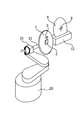
一方、近年は半導体製造工程の微細化に伴い、半導体製造装置の構造が複雑となり、教示のための作業空間が高所になり、あるいは狭くなり作業者が教示点に近づくことが困難となりつつある。これらを解決するためのいわゆるオートティーチングに関する発明が特許文献1に開示されている。
図10は特許文献1に開示されたセンタリング治具の斜視図である。また、図11はセンシング治具の斜視図である。図に示すように、図に示すようにセンタリング治具80の中央には突起形状81が設けられている。また、センシング治具90は中央に穴のあいたドーナツ型の形状をしており穴を挟んで2組の光学式センサ91,92と94,95が、それぞれのビーム光93,96が90度に交わるように配置されている。このセンシング治具90をロボットのハンドに搭載し、センタリング治具80の突起形状81がセンシング治具90の穴に入るように移動する。そしてセンシング治具90を上下、左右、前後に動かし、突起形状81がビーム光93,96をオン・オフする位置を検出し、それによりロボットの教示位置を求めている。
【0003】
【特許文献1】
特開平11−163098号公報
【0004】
【発明が解決しようとする課題】
しかしながら、この従来技術では、突起形状18を検出するために、上述したようにロボットを上下、左右、前後に動かすサーチ動作が必要となり、近年の半導体製造装置においては装置内が高密度化しており、ロボットと装置内の機器との干渉が発生するという問題があった。また突起形状18がビーム光93,96をオン・オフする位置からは教示位置が得られるのみであり、教示位置でのロボットの姿勢や方向までは得ることができないという問題もあった。
そこで、本発明は、ロボットのサーチ動作が不要で、さらに教示位置でのロボットの姿勢や方向に関する教示も可能となる搬送用ロボットおよび搬送用ロボットの教示方法を提供することを目的とするものである。
【0005】
【課題を解決するための手段】
上記の課題を解決するために、本発明は薄板状のワークを載置部に載置して搬送する搬送用ロボットにおいて、前記載置部に載置する教示用治具であって、撮像手段と投光手段を有する教示用治具を備え、前記投光手段はパターン光を検出対象に投光し、前記撮像手段は前記検出対象の画像を撮像し、前記画像に基づいて前記載置部と前記検出対象の距離を求めるものである。
また、薄板状のワークを載置部に載置して搬送する搬送用ロボットの教示方法において、撮像手段と投光手段を有する教示用治具を載置部に載置し、前記投光手段によってパターン光を検出対象に投光し、前記検出対象の画像を前記撮像手段で撮像し、前記画像中の前記パターン光の位置に基づいて前記載置部と前記検出対象の距離を求めて、前記載置部を前記検出対象に対して位置決めするものである。また、撮像手段と投光手段を有する教示用治具を載置部に載置し、前記投光手段によってパターン光を検出対象に投光し、前記検出対象の画像を前記撮像手段で撮像し、前記画像中の前記パターン光の位置と形状に基づいて、前記検出対象に対する前記載置部の相対的な位置と姿勢を求めて、前記載置部の位置と姿勢を決定するものである。撮像手段を有する教示用治具を載置部に載置し、検出対象の特徴部分の画像を前記撮像手段で撮像し、前記画像中の前記特徴部分の位置と形状に基づいて、前記検出対象に対する前記載置部の相対的な位置と姿勢を求めて、前記載置部の位置と姿勢を決定するものである。
また、前記パターン光をスポット光あるいは十字パターン光とするものである。また、前記特徴部分を十字マークあるいは文字パターンとするものである。また、前記検出対象をダミーウェハあるいはマーク付きのダミーウェハとするものである。
【0006】
【発明の実施の形態】
以下に、本発明の実施例を図に基づいて説明する。
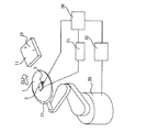
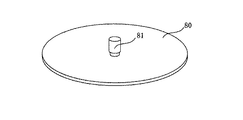
図1は本発明の実施例を示すウェハ搬送装置の構成図である。図において、20はウェハ搬送用ロボットであり、その先端にはウェハを載置するハンド21が装着されている。ウェハ搬送用ロボット20は、回転軸、伸縮軸、上下軸の3軸構成であり、処理ユニット内のウェハ載置用ステージ10にウェハの搬入/搬出動作を行う。この例では、ウェハは載置ステージ10上の3本のピン11の上に置かれる。
教示作業に際しては、ウェハの代わりにハンド21に教示用治具1を載置する。
また教示用治具1はハンド21に載置可能なようにウェハと同一径を有するの円板状をなしている。さらに、図示しないが教示用治具1はハンド21に載置される際に常に一定の向きになるよう位置決め機構を有していて、ハンド21に対する教示冶具1の位置は一定の公差範囲内に収まるようになっている。教示用治具1上には撮像手段のカメラ2と投光手段のレーザ投光器3が設けられている。カメラ2は教示用治具1の中心に下側を撮影するように設置されており、できるだけ小型・軽量であることが望ましい。また、レーザ投光器3は、スポット形や十字形状などのパターン光を照射する。
教示作業では上位制御装置30が、ロボットコントローラ32にロボット20の動作指令や、レーザ投光器3のオン・オフ指令を出す。そしてカメラ2の映像を画像処理装置31で処理し、その結果が上位制御装置30に送られ、ここでロボットの教示位置や姿勢が計算される。なお、ここでは上位制御装置30,画像処理装置31,ロボットコントローラ32を個別に示したが、これらの機能を1体の制御装置に集約してもよい。
【0007】
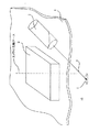
図2は教示用治具1が載置ステージ10上にあるときの教示冶具1の中心付近の斜視図である。レーザ投光器3の光軸4は矢印で表しており、ここではスポット光5を投光している。
図3は、教示用治具1と載置ステージ10の位置関係を説明する側面図である。図において10A,10Bおよび10Cは載置ステージ10の上面を表す線であり、教示冶示具1と載置ステージ間の距離(つまり、載置ステージ10に対する教示冶具1の相対高さ)が変化する状態を示している。
教示冶具1と載置ステージ10間の距離が変わり、点線で示した10A,10B,10Cにあるとき、スポット光5はそれぞれ5A,5B,5Cに位置することが分かる。これらの位置は垂直方向だけでなく水平方向にも移動するため、これをカメラ2で撮像しその画面上の位置から載置ステージ10までの距離が計算できるため、ロボットハンド21の載置ステージ10までの距離方向の教示位置を求めることができる。
【0008】
図4に本発明の第2の実施例を示す教示用治具1の中心付近の斜視図である。ここではレーザ投光器3が十字パターン光6を載置ステージ10に投光している。十字パターン光6の中心60はレーザ投光器3の光軸4上にあり、それぞれのラインの端点を61,62,63,64とする。また端点61,62の光の軌跡を直線41,42で表している。いま、教示用治具1に対して載置ステージ10が、十字パターン光6の端点61,62方向に傾いたとする。この様子を図5に示す。載置ステージ10の傾きが変わり、点線で示した10a,10b,10cにある。十字パターン光6の中心60の位置は、図2,図3の説明と同様に載置ステージ10までの距離を求めることができる。さらに、その形状、具体的には中心60から端点61,62までの長さをカメラ2の画像から計測することにより、幾何学的に載置ステージ10の傾きを計算できる。これによって載置ステージ10までの距離だけでなく、その面と平行になるようロボット20のハンド21の姿勢を教示することができる。
【0009】
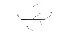
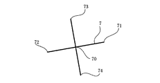
図6は本発明の第3の実施例を示す斜視図である。ここではロボット20は走行軸22に搭載され矢印26方向に移動が可能となっている。ここではレーザ投光器10が投光するパターン光の代わりに、載置ステージ10の面上に位置決め用の十字マーク7が刻印されている。教示作業においてはこの十字マーク7を教示用治具1上のカメラ2で撮像する。図7はカメラ2で撮像した十字マーク7の画像である。ここで、70は十字マーク7の中心を示し、71,72,73,74は各端点である。画像中の中心70の位置が分かれば、載置ステージ10に対する水平方向の位置決めが可能である。さらに、十字マーク7が図8のように画像中で回転していたとすると、端点71,72の方向、あるいは端点73,74の方向を求めると、載置ステージ10に対する教示冶具1の(つまり、ハンド21)の角度が分かるから、ハンド21の挿入方向(図6の矢印25)も計算できる。この値からロボットの回転軸と走行軸26を補正することにより挿入方向の教示が可能となる。さらに十字マークの形状、具体的には中心70から各端点71,72,73,74までの距離を計測することにより、前記第2の実施例と同様に載置ステージ10の傾きが推定できるため、載置ステージ10の面と平行になるようロボット20のハンド21の姿勢を教示することができる。なお、この実施例は、載置ステージ10と水平方向の教示手法であり、実際にはこれに先立って先の実施例で述べた手法により載置ステージ10との距離を調整しておくことが望ましい。
【0010】
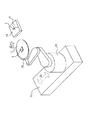
これまでの実施例では、ウェハを置く載置ステージが存在したが、ウェハのエッジを把持して固定する装置、あるいはウェハを縦に置く装置などもあり教示作業はさらに難しくなる。そこで第4の実施例ではこのような場合の教示作業を想定し、ウェハと同形状の薄型治具(ダミーウェハ)を使用する。
図9は本発明の第4の実施例を示す斜視図である。ここでは、縦置きウェハの例でウェハを置くためのウェハスタンド12が設けられている。ロボット20はウェハを立てるための回転軸23が手首にあり、ハンド21を矢印27方向に回転できる。ここでは薄型治具8には中心に十字マーク10がつけられており、あらかじめウェハが載置される状況と同様にウェハスタンド12に置かれている。一方ロボット20のハンド21には教示用治具1を把持している。教示作業ではまず、図2,3で説明したようにレーザ投光器3によりパターン光を薄型治具8に投光し、カメラ2の画像中の位置より薄型治具8との距離を求め、所定の位置にロボットを移動する。さらにこれに薄型治具8上の十字マーク10をカメラ2の画像から計測し、薄型治具8の面に対し中心が合うような教示位置と、さらにハンド21の面が平行となるように回転軸23の教示位置を求める。
【0011】
なお、以上の実施例では、レーザ投光器3からのパターン光の形状や、載置ステージ10および薄型治具8のマークを十字型で説明したが、特に十字型に限定するものではなく、傾きが検出できる形状であればよい。あるいは文字型のパターンであってもよい。
【0012】
【発明の効果】
以上、説明したような本発明は次のような効果を奏する。
請求項1記載の搬送用ロボットによれば、撮像手段を利用することによりロボットのサーチ動作が不要となり、さらに作業者が近づけない箇所の教示が可能となる効果がある。
請求項2記載の搬送用ロボットの制御方法によれば、作業者がウェハ等の搬送の教示位置に接近することが出来ない箇所でも、載置位置とロボットのハンドとの距離を所定の値にできる効果がある。
請求項3ないし請求項8記載の搬送用ロボットの制御方法によれば、載置位置までの距離だけでなく、載置位置の面に対してロボットのハンドの面を平行にする姿勢も教示できる効果がある。
請求項9および請求項10記載の搬送用ロボットの制御方法によれば、薄型治具を用いることにより、ウェハの載置方法がエッジグリップや縦置きの場合でも、教示できる効果がある。
【図面の簡単な説明】
【図1】本発明の実施例を示す斜視図である。
【図2】本発明の実施例を示すの教示用治具の中心付近の斜視図である。
【図3】教示用治具と載置ステージの位置関係を説明する側面図である。
【図4】本発明の第2の実施例を示す教示用治具の中心付近の斜視図である。
【図5】本発明の第2の実施例を示す説明図である。
【図6】本発明の第3の実施例を示す斜視図である。
【図7】本発明の第3の実施例を示す位置決めマークの画像の例である。
【図8】本発明の第3の実施例を示す位置決めマークの別の画像の例である。
【図9】本発明の第4の実施例を示す斜視図である。
【図10】従来技術の例を示すセンタリング治具の斜視図である。
【図11】従来技術の例を示すセンシング治具の斜視図である。
【符号の説明】
1:教示用治具 2:カメラ 3:レーザ投光器 4:レーザ投光器の光軸
5:スポット光 6:十字パターン光 7:載置ステージ上の位置決めマーク
8:薄型治具 9:薄型治具上の位置決めマーク 10:載置ステージ
11:3本ピン 12:縦置きウェハ用のスタンド 20:搬送用ロボット
21:ハンド 22:走行軸 23:ハンド用回転軸
25:ロボットのウェハ挿入方向 26:ロボットの走行方向
27:ハンド用回転軸の回転方向 30:上位制御器 31:画像処理装置
32:ロボットコントローラ 80:センタリング治具 90:センシング治具[0001]
TECHNICAL FIELD OF THE INVENTION
The present invention relates to a transfer robot for transferring a thin work such as a semiconductor wafer. The present invention also relates to a teaching method for a transfer robot, particularly to an auto teaching method.
[0002]
[Prior art]
For teaching (teaching) of a wafer transfer robot in a semiconductor manufacturing apparatus, so-called off-line teaching, in which teaching is performed in a virtual space on a computer using design values related to the dimensions and arrangement of the apparatus, is frequently used. However, even if the transfer robot is actually moved to the design value position due to various factors such as dimensional errors of components constituting the device, assembly errors of the device, etc., the wafer is accurately shifted due to deviation from the predetermined position. It is difficult to position. Therefore, prior to the operation of the semiconductor manufacturing apparatus, it is necessary to teach (teaching) a transfer robot using an actual machine.
On the other hand, in recent years, with the miniaturization of the semiconductor manufacturing process, the structure of the semiconductor manufacturing apparatus has become complicated, and the working space for teaching has been raised or narrowed, and it has become difficult for the operator to approach the teaching point. .
FIG. 10 is a perspective view of the centering jig disclosed in
[0003]
[Patent Document 1]
JP-A-11-163098
[Problems to be solved by the invention]
However, in this prior art, a search operation for moving the robot up and down, left and right, and back and forth is required as described above in order to detect the projection shape 18, and in recent semiconductor manufacturing apparatuses, the inside of the apparatus has been increased in density. However, there has been a problem that interference between the robot and devices in the apparatus occurs. Further, only the teaching position can be obtained from the position where the projection shape 18 turns on / off the
Therefore, an object of the present invention is to provide a transfer robot and a transfer robot teaching method that do not require a robot search operation and that can also teach the posture and direction of the robot at a teaching position. is there.
[0005]
[Means for Solving the Problems]
In order to solve the above-mentioned problem, the present invention relates to a transfer robot for mounting a thin plate-shaped work on a mounting portion and transferring the same, and a teaching jig mounted on the mounting portion, And a teaching jig having a light projecting means, wherein the light projecting means projects the pattern light to a detection target, and the imaging means captures an image of the detection target, and the mounting portion based on the image. And the distance between the detection targets.
Also, in the teaching method of a transfer robot that transfers a thin plate-shaped work by mounting it on a mounting portion, a teaching jig having an imaging unit and a light emitting unit is mounted on the mounting unit, and By projecting the pattern light to the detection target by, the image of the detection target is imaged by the imaging means, based on the position of the pattern light in the image to determine the distance between the mounting portion and the detection target, The positioning unit is positioned with respect to the detection target. Further, a teaching jig having an imaging unit and a light projecting unit is placed on a mounting unit, and the pattern light is projected on the detection target by the light projecting unit, and the image of the detection target is imaged by the imaging unit. A position and a posture of the placement unit relative to the detection target are determined based on a position and a shape of the pattern light in the image, and the position and the posture of the placement unit are determined. A teaching jig having an imaging unit is placed on a mounting unit, an image of a characteristic portion of the detection target is captured by the imaging unit, and the detection target is detected based on the position and shape of the characteristic portion in the image. The position and orientation of the placement unit are determined by calculating the relative position and orientation of the placement unit with respect to.
Further, the pattern light is a spot light or a cross pattern light. Further, the characteristic portion is a cross mark or a character pattern. Further, the detection target is a dummy wafer or a marked dummy wafer.
[0006]
BEST MODE FOR CARRYING OUT THE INVENTION
Hereinafter, an embodiment of the present invention will be described with reference to the drawings.
FIG. 1 is a configuration diagram of a wafer transfer device showing an embodiment of the present invention. In the drawing,
In the teaching operation, the
The
In the teaching operation, the
[0007]
FIG. 2 is a perspective view of the vicinity of the center of the
FIG. 3 is a side view illustrating the positional relationship between the
It can be seen that when the distance between the
[0008]
FIG. 4 is a perspective view near the center of a
[0009]
FIG. 6 is a perspective view showing a third embodiment of the present invention. Here, the
[0010]
In the embodiments described so far, there is a mounting stage on which a wafer is placed. However, there is a device for holding and fixing the edge of the wafer, or a device for placing the wafer vertically, and the teaching work becomes more difficult. Therefore, in the fourth embodiment, a teaching jig in such a case is assumed, and a thin jig (dummy wafer) having the same shape as the wafer is used.
FIG. 9 is a perspective view showing a fourth embodiment of the present invention. Here, a
[0011]
In the above-described embodiment, the shape of the pattern light from the
[0012]
【The invention's effect】
The present invention as described above has the following effects.
According to the transfer robot according to the first aspect, the use of the imaging means eliminates the need for a search operation of the robot, and further has an effect that it is possible to teach a location that the worker cannot approach.
According to the control method of the transfer robot according to the second aspect, the distance between the mounting position and the hand of the robot is set to a predetermined value even at a location where the worker cannot approach the transfer teaching position of the wafer or the like. There is an effect that can be done.
According to the control method of the transfer robot according to the third to eighth aspects, not only the distance to the mounting position but also the attitude of making the robot hand surface parallel to the mounting position surface can be taught. effective.
According to the transfer robot control method according to the ninth and tenth aspects, the use of a thin jig has an effect that teaching can be performed even when the wafer mounting method is an edge grip or a vertical mounting.
[Brief description of the drawings]
FIG. 1 is a perspective view showing an embodiment of the present invention.
FIG. 2 is a perspective view showing the vicinity of the center of the teaching jig according to the embodiment of the present invention.
FIG. 3 is a side view illustrating a positional relationship between a teaching jig and a mounting stage.
FIG. 4 is a perspective view of the vicinity of the center of a teaching jig showing a second embodiment of the present invention.
FIG. 5 is an explanatory diagram showing a second embodiment of the present invention.
FIG. 6 is a perspective view showing a third embodiment of the present invention.
FIG. 7 is an example of an image of a positioning mark showing a third embodiment of the present invention.
FIG. 8 is an example of another image of a positioning mark showing the third embodiment of the present invention.
FIG. 9 is a perspective view showing a fourth embodiment of the present invention.
FIG. 10 is a perspective view of a centering jig showing an example of the related art.
FIG. 11 is a perspective view of a sensing jig showing an example of the related art.
[Explanation of symbols]
1: Teaching jig 2: Camera 3: Laser projector 4: Optical axis of laser projector 5: Spot light 6: Cross pattern light 7: Positioning mark on mounting stage 8: Thin jig 9: On thin jig Positioning mark 10: Mounting stage 11: Three pins 12: Stand for vertical wafer 20: Transfer robot 21: Hand 22: Travel axis 23: Hand rotation axis 25: Robot wafer insertion direction 26: Robot travel Direction 27: Rotation direction of hand rotary shaft 30: Host controller 31: Image processing device 32: Robot controller 80: Centering jig 90: Sensing jig
Claims (10)
前記載置部に載置する教示用治具であって、撮像手段と投光手段を有する教示用治具を備え、
前記投光手段はパターン光を検出対象に投光し、前記撮像手段は前記検出対象の画像を撮像し、前記画像に基づいて前記載置部と前記検出対象の距離を求めることを特徴とする搬送用ロボット。In a transfer robot that transfers a thin plate-shaped work by mounting it on a mounting portion,
A teaching jig to be mounted on the mounting section, including a teaching jig having an imaging unit and a light emitting unit,
The light projecting unit projects pattern light onto a detection target, the imaging unit captures an image of the detection target, and calculates a distance between the placement unit and the detection target based on the image. Transfer robot.
撮像手段と投光手段を有する教示用治具を載置部に載置し、
前記投光手段によってパターン光を検出対象に投光し、
前記検出対象の画像を前記撮像手段で撮像し、
前記画像中の前記パターン光の位置に基づいて前記載置部と前記検出対象の距離を求めて、前記載置部を前記検出対象に対して位置決めすることを特徴とする搬送用ロボットの教示方法。In a teaching method of a transport robot that transports a thin plate-shaped work by mounting the work on a mounting portion,
A teaching jig having an imaging unit and a light emitting unit is mounted on the mounting unit,
By projecting the pattern light on the detection target by the light emitting means,
Imaging the image of the detection target by the imaging means,
A method of teaching a transport robot, comprising: determining a distance between the placement unit and the detection target based on a position of the pattern light in the image, and positioning the placement unit with respect to the detection target. .
撮像手段と投光手段を有する教示用治具を載置部に載置し、
前記投光手段によってパターン光を検出対象に投光し、
前記検出対象の画像を前記撮像手段で撮像し、
前記画像中の前記パターン光の位置と形状に基づいて、前記検出対象に対する前記載置部の相対的な位置と姿勢を求めて、前記載置部の位置と姿勢を決定することを特徴とする搬送用ロボットの教示方法。In a teaching method of a transport robot that transports a thin plate-shaped work by mounting the work on a mounting portion,
A teaching jig having an imaging unit and a light emitting unit is mounted on the mounting unit,
By projecting the pattern light on the detection target by the light emitting means,
Imaging the image of the detection target by the imaging means,
Based on a position and a shape of the pattern light in the image, a relative position and a posture of the placement unit with respect to the detection target are obtained, and the position and the posture of the placement unit are determined. Teaching method of transfer robot.
撮像手段を有する教示用治具を載置部に載置し、
検出対象の特徴部分の画像を前記撮像手段で撮像し、
前記画像中の前記特徴部分の位置と形状に基づいて、前記検出対象に対する前記載置部の相対的な位置と姿勢を求めて、前記載置部の位置と姿勢を決定することを特徴とする搬送用ロボットの教示方法。In a teaching method of a transport robot that transports a thin plate-shaped work by mounting the work on a mounting portion,
Place the teaching jig having the imaging means on the mounting portion,
An image of a characteristic portion to be detected is captured by the imaging unit,
Based on the position and shape of the characteristic portion in the image, a relative position and orientation of the placement unit with respect to the detection target are obtained, and the position and orientation of the placement unit are determined. Teaching method of transfer robot.
Priority Applications (1)
| Application Number | Priority Date | Filing Date | Title |
|---|---|---|---|
| JP2003068726A JP2004276151A (en) | 2003-03-13 | 2003-03-13 | Transfer robot and teaching method for transfer robot |
Applications Claiming Priority (1)
| Application Number | Priority Date | Filing Date | Title |
|---|---|---|---|
| JP2003068726A JP2004276151A (en) | 2003-03-13 | 2003-03-13 | Transfer robot and teaching method for transfer robot |
Publications (2)
| Publication Number | Publication Date |
|---|---|
| JP2004276151A true JP2004276151A (en) | 2004-10-07 |
| JP2004276151A5 JP2004276151A5 (en) | 2006-03-16 |
Family
ID=33285979
Family Applications (1)
| Application Number | Title | Priority Date | Filing Date |
|---|---|---|---|
| JP2003068726A Pending JP2004276151A (en) | 2003-03-13 | 2003-03-13 | Transfer robot and teaching method for transfer robot |
Country Status (1)
| Country | Link |
|---|---|
| JP (1) | JP2004276151A (en) |
Cited By (18)
| Publication number | Priority date | Publication date | Assignee | Title |
|---|---|---|---|---|
| US7283255B2 (en) | 2002-02-06 | 2007-10-16 | Cyberoptics Semiconductor, Inc. | Wireless substrate-like sensor |
| WO2008051544A1 (en) * | 2006-10-23 | 2008-05-02 | Cyberoptics Semiconductor, Inc. | Improved calibration of a substrate handling robot |
| JP2008522213A (en) * | 2005-03-02 | 2008-06-26 | セミシスコ・カンパニー・リミテッド | Glass substrate edge defect and discolor inspection apparatus and method |
| JPWO2006117840A1 (en) * | 2005-04-27 | 2008-12-18 | 平田機工株式会社 | Work transfer position teaching device and teaching method for robot |
| US7778793B2 (en) | 2007-03-12 | 2010-08-17 | Cyberoptics Semiconductor, Inc. | Wireless sensor for semiconductor processing systems |
| US7804306B2 (en) | 2006-02-21 | 2010-09-28 | CyterOptics Semiconductor, Inc. | Capacitive distance sensing in semiconductor processing tools |
| CN101996479A (en) * | 2009-08-07 | 2011-03-30 | 台湾积体电路制造股份有限公司 | Apparatus and method for fabricating semiconductor device |
| US8823933B2 (en) | 2006-09-29 | 2014-09-02 | Cyberoptics Corporation | Substrate-like particle sensor |
| JP2017183647A (en) * | 2016-03-31 | 2017-10-05 | 株式会社荏原製作所 | Teaching device and teaching method |
| KR101927695B1 (en) | 2016-09-01 | 2018-12-12 | 세메스 주식회사 | Method for correcting pose of transfer robot |
| CN109716500A (en) * | 2016-09-28 | 2019-05-03 | 川崎重工业株式会社 | The position teaching methodology of robot, the control device of robot and robot |
| WO2019102822A1 (en) * | 2017-11-27 | 2019-05-31 | アズビル株式会社 | Pointer device |
| US10632279B2 (en) | 2016-08-30 | 2020-04-28 | Dentsu Inc. | Meditation support device and meditation support system |
| TWI694045B (en) * | 2015-11-17 | 2020-05-21 | 日商大福股份有限公司 | Article transport facility |
| CN112735251A (en) * | 2020-12-31 | 2021-04-30 | 慧眼自动化科技(广州)有限公司 | Teaching show production system |
| JP2021521651A (en) * | 2018-04-24 | 2021-08-26 | サイバーオプティクス コーポレーション | Wireless substrate-like teaching sensor for semiconductor processing |
| CN114180300A (en) * | 2020-09-15 | 2022-03-15 | 株式会社斯库林集团 | Workpiece receiving device, workpiece conveying device, inspection device, placement support method, and inspection method |
| JP7474688B2 (en) | 2020-12-03 | 2024-04-25 | 東京エレクトロン株式会社 | Correction method and substrate transport device |
Citations (6)
| Publication number | Priority date | Publication date | Assignee | Title |
|---|---|---|---|---|
| JPH0477806A (en) * | 1990-07-13 | 1992-03-11 | Toyota Motor Corp | Detecting device for position error of robot |
| JPH0588741A (en) * | 1991-09-26 | 1993-04-09 | Shin Meiwa Ind Co Ltd | Teaching device for industrial robot and controlling method for its position |
| JPH08272425A (en) * | 1995-03-29 | 1996-10-18 | Fanuc Ltd | Method to teach coordinate system to robot in non-contact |
| JP2001158507A (en) * | 1999-09-21 | 2001-06-12 | Shinko Electric Co Ltd | Method and device for teaching robot for stoker, and storage medium |
| JP2001210692A (en) * | 2000-01-26 | 2001-08-03 | Ebara Corp | Teaching method |
| JP2002307348A (en) * | 2001-04-13 | 2002-10-23 | Yaskawa Electric Corp | Teaching method and teaching plate for wafer carrying robot |
-
2003
- 2003-03-13 JP JP2003068726A patent/JP2004276151A/en active Pending
Patent Citations (6)
| Publication number | Priority date | Publication date | Assignee | Title |
|---|---|---|---|---|
| JPH0477806A (en) * | 1990-07-13 | 1992-03-11 | Toyota Motor Corp | Detecting device for position error of robot |
| JPH0588741A (en) * | 1991-09-26 | 1993-04-09 | Shin Meiwa Ind Co Ltd | Teaching device for industrial robot and controlling method for its position |
| JPH08272425A (en) * | 1995-03-29 | 1996-10-18 | Fanuc Ltd | Method to teach coordinate system to robot in non-contact |
| JP2001158507A (en) * | 1999-09-21 | 2001-06-12 | Shinko Electric Co Ltd | Method and device for teaching robot for stoker, and storage medium |
| JP2001210692A (en) * | 2000-01-26 | 2001-08-03 | Ebara Corp | Teaching method |
| JP2002307348A (en) * | 2001-04-13 | 2002-10-23 | Yaskawa Electric Corp | Teaching method and teaching plate for wafer carrying robot |
Cited By (24)
| Publication number | Priority date | Publication date | Assignee | Title |
|---|---|---|---|---|
| US7289230B2 (en) | 2002-02-06 | 2007-10-30 | Cyberoptics Semiconductors, Inc. | Wireless substrate-like sensor |
| US7283255B2 (en) | 2002-02-06 | 2007-10-16 | Cyberoptics Semiconductor, Inc. | Wireless substrate-like sensor |
| JP2008522213A (en) * | 2005-03-02 | 2008-06-26 | セミシスコ・カンパニー・リミテッド | Glass substrate edge defect and discolor inspection apparatus and method |
| JPWO2006117840A1 (en) * | 2005-04-27 | 2008-12-18 | 平田機工株式会社 | Work transfer position teaching device and teaching method for robot |
| US7804306B2 (en) | 2006-02-21 | 2010-09-28 | CyterOptics Semiconductor, Inc. | Capacitive distance sensing in semiconductor processing tools |
| US8823933B2 (en) | 2006-09-29 | 2014-09-02 | Cyberoptics Corporation | Substrate-like particle sensor |
| WO2008051544A1 (en) * | 2006-10-23 | 2008-05-02 | Cyberoptics Semiconductor, Inc. | Improved calibration of a substrate handling robot |
| US7778793B2 (en) | 2007-03-12 | 2010-08-17 | Cyberoptics Semiconductor, Inc. | Wireless sensor for semiconductor processing systems |
| CN101996479A (en) * | 2009-08-07 | 2011-03-30 | 台湾积体电路制造股份有限公司 | Apparatus and method for fabricating semiconductor device |
| TWI694045B (en) * | 2015-11-17 | 2020-05-21 | 日商大福股份有限公司 | Article transport facility |
| TWI713721B (en) * | 2016-03-31 | 2020-12-21 | 日商荏原製作所股份有限公司 | Teaching system, teaching method, cleaning device, memory media and maintenance kit |
| JP2017183647A (en) * | 2016-03-31 | 2017-10-05 | 株式会社荏原製作所 | Teaching device and teaching method |
| US10845777B2 (en) | 2016-03-31 | 2020-11-24 | Ebara Corporation | Teaching device and teaching method |
| US10632279B2 (en) | 2016-08-30 | 2020-04-28 | Dentsu Inc. | Meditation support device and meditation support system |
| KR101927695B1 (en) | 2016-09-01 | 2018-12-12 | 세메스 주식회사 | Method for correcting pose of transfer robot |
| CN109716500A (en) * | 2016-09-28 | 2019-05-03 | 川崎重工业株式会社 | The position teaching methodology of robot, the control device of robot and robot |
| WO2019102822A1 (en) * | 2017-11-27 | 2019-05-31 | アズビル株式会社 | Pointer device |
| JP2021521651A (en) * | 2018-04-24 | 2021-08-26 | サイバーオプティクス コーポレーション | Wireless substrate-like teaching sensor for semiconductor processing |
| US11468590B2 (en) | 2018-04-24 | 2022-10-11 | Cyberoptics Corporation | Wireless substrate-like teaching sensor for semiconductor processing |
| JP7161236B2 (en) | 2018-04-24 | 2022-10-26 | サイバーオプティクス コーポレーション | Wireless substrate-like teaching sensor for semiconductor processing |
| CN114180300A (en) * | 2020-09-15 | 2022-03-15 | 株式会社斯库林集团 | Workpiece receiving device, workpiece conveying device, inspection device, placement support method, and inspection method |
| JP7474688B2 (en) | 2020-12-03 | 2024-04-25 | 東京エレクトロン株式会社 | Correction method and substrate transport device |
| CN112735251A (en) * | 2020-12-31 | 2021-04-30 | 慧眼自动化科技(广州)有限公司 | Teaching show production system |
| CN112735251B (en) * | 2020-12-31 | 2023-04-07 | 慧眼自动化科技(广州)有限公司 | Teaching show production system |
Similar Documents
| Publication | Publication Date | Title |
|---|---|---|
| JP2004276151A (en) | Transfer robot and teaching method for transfer robot | |
| JP4257570B2 (en) | Transfer robot teaching device and transfer robot teaching method | |
| US20010055069A1 (en) | One camera system for component to substrate registration | |
| JP5272617B2 (en) | Robot apparatus and control method of robot apparatus | |
| JP6276449B1 (en) | Substrate processing apparatus, control method for substrate processing apparatus, and storage medium storing program | |
| WO2015045649A1 (en) | Component mounting device | |
| JP2003298294A (en) | Electronic circuit component mounting system | |
| JP6404957B2 (en) | Machining system with a robot that transports workpieces to the processing machine | |
| JP6784151B2 (en) | Plate-shaped body processing method and plate-shaped body processing equipment | |
| WO2015145864A1 (en) | Position displacement detection method, position displacement detection device, drawing device, and substrate inspection device | |
| JP7093255B2 (en) | Mounting device and mounting method | |
| JP2004288824A (en) | Method for calibrating electronic-part mounting device and device using its method | |
| CN113905859B (en) | Robot control system and robot control method | |
| JP2008083520A (en) | Exposure apparatus and alignment method | |
| JP4631497B2 (en) | Proximity exposure equipment | |
| JP2006080197A (en) | Method for correcting place of attraction nozzle in electronic-part mounting device | |
| JP2003145004A (en) | Apparatus for detecting deviation of nozzle position and apparatus for applying material using the same | |
| JPH0283183A (en) | Setting method for position of articulated robot | |
| JP5629540B2 (en) | Alignment unit, substrate processing apparatus, and alignment method | |
| JP4901451B2 (en) | Component mounting equipment | |
| JP2000068696A (en) | Part recognition/mounting device and part recognition method | |
| JP3039645B1 (en) | Electronic component position recognition method and device | |
| JP6151512B2 (en) | Optical axis tilt measuring jig and optical axis tilt measuring method using the same | |
| JPH02142158A (en) | Wafer positioning apparatus and method for returning wafer to original position | |
| JP2008260599A (en) | Method for adjusting conveying face of semiconductor wafer conveying system, semiconductor wafer conveying system using it, and semiconductor manufacturing device |
Legal Events
| Date | Code | Title | Description |
|---|---|---|---|
| A521 | Written amendment |
Free format text: JAPANESE INTERMEDIATE CODE: A523 Effective date: 20060127 |
|
| A621 | Written request for application examination |
Free format text: JAPANESE INTERMEDIATE CODE: A621 Effective date: 20060127 |
|
| A977 | Report on retrieval |
Free format text: JAPANESE INTERMEDIATE CODE: A971007 Effective date: 20070718 |
|
| A131 | Notification of reasons for refusal |
Free format text: JAPANESE INTERMEDIATE CODE: A131 Effective date: 20070725 |
|
| A02 | Decision of refusal |
Free format text: JAPANESE INTERMEDIATE CODE: A02 Effective date: 20071115 |